Operation of a multi-slice processor implementing a load/store unit maintaining rejected instructions
Chadha , et al.
U.S. patent number 10,268,518 [Application Number 15/997,863] was granted by the patent office on 2019-04-23 for operation of a multi-slice processor implementing a load/store unit maintaining rejected instructions. This patent grant is currently assigned to International Business Machines Corporation. The grantee listed for this patent is International Business Machines Corporation. Invention is credited to Sundeep Chadha, Robert A. Cordes, David A. Hrusecky, Hung Q. Le, Elizabeth A. McGlone.


| United States Patent | 10,268,518 |
| Chadha , et al. | April 23, 2019 |
Operation of a multi-slice processor implementing a load/store unit maintaining rejected instructions
Abstract
Operation of a multi-slice processor that includes a plurality of execution slices, a plurality of load/store slices, and one or more instruction sequencing units, where operation includes: receiving, at a load/store slice from an instruction sequencing unit, a instruction to be issued; determining, at the load/store slice, a rejection condition for the instruction; and responsive to determining the rejection condition for the instruction, maintaining state information for the instruction in the load/store slice instead of notifying the instruction sequencing unit of a rejection of the instruction.
| Inventors: | Chadha; Sundeep (Austin, TX), Cordes; Robert A. (Austin, TX), Hrusecky; David A. (Cedar Park, TX), Le; Hung Q. (Austin, TX), McGlone; Elizabeth A. (Oronoco, MN) | ||||||||||
|---|---|---|---|---|---|---|---|---|---|---|---|
| Applicant: |
|
||||||||||
| Assignee: | International Business Machines
Corporation (Armonk, NY) |
||||||||||
| Family ID: | 60295120 | ||||||||||
| Appl. No.: | 15/997,863 | ||||||||||
| Filed: | June 5, 2018 |
Prior Publication Data
| Document Identifier | Publication Date | |
|---|---|---|
| US 20180285161 A1 | Oct 4, 2018 | |
Related U.S. Patent Documents
| Application Number | Filing Date | Patent Number | Issue Date | ||
|---|---|---|---|---|---|
| 15152257 | May 11, 2016 | 10037229 | |||
| Current U.S. Class: | 1/1 |
| Current CPC Class: | G06F 9/5027 (20130101); G06F 9/3836 (20130101); G06F 9/30043 (20130101); G06F 9/3891 (20130101); G06F 12/0875 (20130101); G06F 9/3861 (20130101); G06F 2212/452 (20130101) |
| Current International Class: | G06F 9/46 (20060101); G06F 12/0875 (20160101); G06F 9/30 (20180101); G06F 9/50 (20060101); G06F 9/38 (20180101) |
References Cited [Referenced By]
U.S. Patent Documents
| 4858113 | August 1989 | Saccardi |
| 5055999 | October 1991 | Frank et al. |
| 5095424 | March 1992 | Woffinden et al. |
| 5353426 | October 1994 | Patel et al. |
| 5418922 | May 1995 | Liu |
| 5471593 | November 1995 | Branigin |
| 5475856 | December 1995 | Kogge |
| 5553305 | September 1996 | Gregor et al. |
| 5630149 | May 1997 | Bluhm |
| 5664215 | September 1997 | Burgess et al. |
| 5680597 | October 1997 | Kumar et al. |
| 5724536 | March 1998 | Abramson et al. |
| 5809522 | September 1998 | Novak et al. |
| 5809530 | September 1998 | Samra et al. |
| 5822602 | October 1998 | Thusoo |
| 5897651 | April 1999 | Cheong et al. |
| 5909588 | June 1999 | Fujimura et al. |
| 5913048 | June 1999 | Cheong et al. |
| 5996068 | November 1999 | Dwyer, III et al. |
| 6021485 | February 2000 | Feiste et al. |
| 6026478 | February 2000 | Dowling |
| 6044448 | March 2000 | Agrawal et al. |
| 6073215 | June 2000 | Snyder |
| 6073231 | June 2000 | Bluhm et al. |
| 6092175 | July 2000 | Levy et al. |
| 6098166 | August 2000 | Leibholz et al. |
| 6108753 | August 2000 | Bossen et al. |
| 6112019 | August 2000 | Chamdani et al. |
| 6119203 | September 2000 | Snyder et al. |
| 6138230 | October 2000 | Hervin et al. |
| 6145054 | November 2000 | Mehrotra et al. |
| 6170051 | January 2001 | Dowling |
| 6269427 | January 2001 | Kuttanna et al. |
| 6212544 | April 2001 | Borkenhagen et al. |
| 6237081 | May 2001 | Le et al. |
| 6286027 | September 2001 | Dwyer, III et al. |
| 6311261 | October 2001 | Chamdani et al. |
| 6336168 | January 2002 | Frederick, Jr. et al. |
| 6336183 | January 2002 | Le et al. |
| 6356918 | March 2002 | Chuang et al. |
| 6381676 | April 2002 | Aglietti et al. |
| 6418513 | July 2002 | Arimilli et al. |
| 6418525 | July 2002 | Charney et al. |
| 6425073 | July 2002 | Roussel et al. |
| 6463524 | October 2002 | Delaney et al. |
| 6487578 | November 2002 | Ranganathan |
| 6549930 | April 2003 | Chrysos et al. |
| 6553480 | April 2003 | Cheong et al. |
| 6564315 | May 2003 | Keller et al. |
| 6654876 | November 2003 | Le et al. |
| 6728866 | April 2004 | Kahle et al. |
| 6732236 | May 2004 | Favor |
| 6839828 | January 2005 | Gschwind et al. |
| 6847578 | January 2005 | Ayukawa et al. |
| 6868491 | March 2005 | Moore |
| 6883107 | April 2005 | Rodgers et al. |
| 6901504 | May 2005 | Luick |
| 6944744 | September 2005 | Ahmed et al. |
| 6948051 | September 2005 | Rivers et al. |
| 6954846 | October 2005 | Leibholz et al. |
| 6978459 | December 2005 | Dennis et al. |
| 7020763 | March 2006 | Saulsbury et al. |
| 7024543 | April 2006 | Grisenthwaite et al. |
| 7086053 | August 2006 | Long et al. |
| 7093105 | August 2006 | Webb, Jr. et al. |
| 7100028 | August 2006 | McGrath et al. |
| 7100157 | August 2006 | Collard |
| 7114163 | September 2006 | Hardin et al. |
| 7124160 | October 2006 | Saulsbury et al. |
| 7155600 | December 2006 | Burky et al. |
| 7191320 | March 2007 | Hooker et al. |
| 7263624 | August 2007 | Marchand et al. |
| 7290261 | October 2007 | Burky et al. |
| 7302527 | November 2007 | Barrick et al. |
| 7350056 | March 2008 | Abernathy et al. |
| 7386704 | June 2008 | Schulz et al. |
| 7395419 | July 2008 | Gonion |
| 7398374 | July 2008 | Delano |
| 7401188 | July 2008 | Matthews |
| 7469318 | December 2008 | Chung et al. |
| 7478198 | January 2009 | Latorre et al. |
| 7478225 | January 2009 | Brooks et al. |
| 7490220 | February 2009 | Balasubramonian et al. |
| 7509484 | March 2009 | Golla et al. |
| 7512724 | March 2009 | Dennis et al. |
| 7565652 | July 2009 | Janssen et al. |
| 7600096 | October 2009 | Parthasarathy et al. |
| 7669035 | February 2010 | Young et al. |
| 7669036 | February 2010 | Brown et al. |
| 7685410 | March 2010 | Shen et al. |
| 7694112 | April 2010 | Barowski et al. |
| 7707390 | April 2010 | Ozer et al. |
| 7721069 | May 2010 | Ramchandran et al. |
| 7793278 | September 2010 | Du et al. |
| 7836317 | November 2010 | Marchand et al. |
| 7889204 | February 2011 | Hansen et al. |
| 7890735 | February 2011 | Tran |
| 7926023 | April 2011 | Okawa et al. |
| 7949859 | May 2011 | Kalla et al. |
| 7975134 | July 2011 | Gonion |
| 7987344 | July 2011 | Hansen et al. |
| 8028152 | September 2011 | Glew |
| 8041928 | October 2011 | Burky et al. |
| 8046566 | October 2011 | Abernathy et al. |
| 8074224 | December 2011 | Nordquist et al. |
| 8099556 | January 2012 | Ghosh et al. |
| 8103852 | January 2012 | Bishop et al. |
| 8108656 | January 2012 | Katragadda et al. |
| 8131942 | March 2012 | Harris et al. |
| 8131980 | March 2012 | Hall et al. |
| 8135942 | March 2012 | Abernathy et al. |
| 8140832 | March 2012 | Mejdrich et al. |
| 8141088 | March 2012 | Morishita et al. |
| 8151012 | April 2012 | Kim et al. |
| 8166282 | April 2012 | Madriles et al. |
| 8184686 | May 2012 | Wall et al. |
| 8219783 | July 2012 | Hara |
| 8219787 | July 2012 | Lien et al. |
| 8243866 | August 2012 | Huang et al. |
| 8250341 | August 2012 | Schulz et al. |
| 8271765 | September 2012 | Bose et al. |
| 8325793 | December 2012 | Zhong |
| 8335892 | December 2012 | Minkin et al. |
| 8386751 | February 2013 | Ramchandran et al. |
| 8402256 | March 2013 | Arakawa |
| 8412914 | April 2013 | Gonion |
| 8464025 | June 2013 | Yamaguchi et al. |
| 8489791 | July 2013 | Byrne et al. |
| 8521992 | August 2013 | Alexander et al. |
| 8555039 | October 2013 | Rychlik |
| 8578140 | November 2013 | Yokoi |
| 8654884 | February 2014 | Kerr |
| 8656401 | February 2014 | Venkataramanan et al. |
| 8683182 | March 2014 | Hansen et al. |
| 8713263 | April 2014 | Bryant |
| 8793435 | July 2014 | Ashcraft et al. |
| 8806135 | August 2014 | Ashcraft et al. |
| 8850121 | September 2014 | Ashcraft et al. |
| 8929496 | January 2015 | Lee et al. |
| 8935513 | January 2015 | Guthrie et al. |
| 8966232 | February 2015 | Tran |
| 8984264 | March 2015 | Karlsson et al. |
| 9069563 | June 2015 | Konigsburg et al. |
| 9207995 | December 2015 | Boersma et al. |
| 9223709 | December 2015 | O'Bleness et al. |
| 9519484 | December 2016 | Stark |
| 9665372 | May 2017 | Eisen et al. |
| 9672043 | June 2017 | Eisen et al. |
| 9690585 | June 2017 | Eisen et al. |
| 9690586 | June 2017 | Eisen et al. |
| 9720696 | August 2017 | Chu et al. |
| 9740486 | August 2017 | Boersma et al. |
| 9760375 | September 2017 | Boersma et al. |
| 9934033 | April 2018 | Cordes et al. |
| 9940133 | April 2018 | Cordes et al. |
| 9983875 | May 2018 | Chadha et al. |
| 10037211 | July 2018 | Fernsler et al. |
| 10037229 | July 2018 | Fernsler et al. |
| 10042647 | August 2018 | Eickemeyer et al. |
| 10042770 | August 2018 | Chadha et al. |
| 2002/0078302 | June 2002 | Favor |
| 2002/0138700 | September 2002 | Holmberg |
| 2002/0194251 | December 2002 | Richter et al. |
| 2003/0120882 | June 2003 | Granston et al. |
| 2003/0163669 | August 2003 | Delano |
| 2003/0182537 | September 2003 | Le et al. |
| 2004/0111594 | June 2004 | Feiste et al. |
| 2004/0162966 | August 2004 | James Webb, Jr. et al. |
| 2004/0172521 | September 2004 | Hooker et al. |
| 2004/0181652 | September 2004 | Ahmed et al. |
| 2004/0216101 | October 2004 | Burky et al. |
| 2005/0060518 | March 2005 | Augsburg et al. |
| 2005/0138290 | June 2005 | Hammarlund et al. |
| 2006/0095710 | May 2006 | Pires Dos Reis Moreira et al. |
| 2006/0106923 | May 2006 | Balasubramonian et al. |
| 2006/0143513 | June 2006 | Hillman et al. |
| 2007/0022277 | January 2007 | Iwamura et al. |
| 2007/0079303 | April 2007 | Du et al. |
| 2007/0101102 | May 2007 | Dierks, Jr. et al. |
| 2007/0106874 | May 2007 | Pan et al. |
| 2007/0180221 | August 2007 | Abernathy et al. |
| 2007/0204137 | August 2007 | Tran |
| 2008/0098260 | April 2008 | Okawa et al. |
| 2008/0104375 | May 2008 | Hansen et al. |
| 2008/0133885 | June 2008 | Glew |
| 2008/0162889 | July 2008 | Cascaval et al. |
| 2008/0162895 | July 2008 | Luick |
| 2008/0172548 | July 2008 | Caprioli et al. |
| 2008/0270749 | October 2008 | Ozer et al. |
| 2008/0307182 | December 2008 | Arimilli et al. |
| 2008/0313424 | December 2008 | Gschwind |
| 2009/0037698 | February 2009 | Nguyen |
| 2009/0113182 | April 2009 | Abernathy et al. |
| 2009/0198921 | August 2009 | Chen et al. |
| 2009/0265532 | October 2009 | Caprioli et al. |
| 2009/0282225 | November 2009 | Caprioli et al. |
| 2009/0300319 | December 2009 | Cohen et al. |
| 2010/0100685 | April 2010 | Kurosawa et al. |
| 2010/0161945 | June 2010 | Burky et al. |
| 2010/0191940 | July 2010 | Mejdrich et al. |
| 2010/0262781 | October 2010 | Hrusecky et al. |
| 2011/0078697 | March 2011 | Smittle et al. |
| 2012/0060015 | March 2012 | Eichenberger et al. |
| 2012/0060016 | March 2012 | Eichenberger et al. |
| 2012/0066482 | March 2012 | Gonion |
| 2012/0110271 | May 2012 | Boersma et al. |
| 2012/0226865 | September 2012 | Choi et al. |
| 2012/0246450 | September 2012 | Abdallah |
| 2013/0254488 | September 2013 | Kaxiras et al. |
| 2013/0305022 | November 2013 | Eisen et al. |
| 2013/0339670 | December 2013 | Busaba |
| 2014/0025933 | January 2014 | Venkataramanan et al. |
| 2014/0040599 | February 2014 | Fleischer et al. |
| 2014/0075159 | March 2014 | Frigo et al. |
| 2014/0189243 | July 2014 | Cuesta et al. |
| 2014/0215189 | July 2014 | Airaud et al. |
| 2014/0223144 | August 2014 | Heil et al. |
| 2014/0244239 | August 2014 | Nicholson et al. |
| 2014/0281408 | September 2014 | Zeng |
| 2014/0325188 | October 2014 | Ogasawara |
| 2015/0046662 | February 2015 | Heinrich et al. |
| 2015/0121010 | April 2015 | Kaplan et al. |
| 2015/0121046 | April 2015 | Kunjan et al. |
| 2015/0134935 | May 2015 | Blasco |
| 2015/0199272 | July 2015 | Goel et al. |
| 2015/0324204 | November 2015 | Eisen et al. |
| 2015/0324205 | November 2015 | Eisen et al. |
| 2015/0324206 | November 2015 | Eisen et al. |
| 2015/0324207 | November 2015 | Eisen et al. |
| 2016/0070571 | March 2016 | Boersma et al. |
| 2016/0070574 | March 2016 | Boersma et al. |
| 2016/0092231 | March 2016 | Chu et al. |
| 2016/0092276 | March 2016 | Chu et al. |
| 2016/0103715 | April 2016 | Sethia et al. |
| 2016/0202986 | July 2016 | Ayub et al. |
| 2016/0202988 | July 2016 | Ayub et al. |
| 2016/0202989 | July 2016 | Eisen et al. |
| 2016/0202990 | July 2016 | Brownscheidle et al. |
| 2016/0202991 | July 2016 | Eisen et al. |
| 2016/0202992 | July 2016 | Brownscheidle et al. |
| 2017/0168837 | June 2017 | Eisen et al. |
| 2017/0255465 | September 2017 | Chadha et al. |
| 2017/0277542 | September 2017 | Fernsler et al. |
| 2017/0277543 | September 2017 | McGlone et al. |
| 2017/0300328 | October 2017 | Cordes et al. |
| 2017/0329641 | November 2017 | Chadha et al. |
| 2017/0329713 | November 2017 | Chadha et al. |
| 2017/0351521 | December 2017 | Hrusecky |
| 2017/0357507 | December 2017 | Cordes et al. |
| 2017/0357508 | December 2017 | Cordes et al. |
| 2017/0371658 | December 2017 | Eickemeyer et al. |
| 2018/0039577 | February 2018 | Chadha et al. |
| 2018/0067746 | March 2018 | Chu et al. |
| 101021778 | Aug 2007 | CN | |||
| 101676865 | Mar 2010 | CN | |||
| 101876892 | Nov 2010 | CN | |||
| 102004719 | Apr 2011 | CN | |||
| 1212680 | Jul 2007 | EP | |||
| 2356324 | May 2001 | GB | |||
| 2356324 | Oct 2001 | GB | |||
| 2009157887 | Jul 2009 | JP | |||
| WO-2015/067118 | May 2015 | WO | |||
Other References
|
Anonymous, A Novel Data Prefetch Method Under Heterogeneous Architecture, IP.com Prior Art Database Technical Disclosure No. 000224167 (online), Dec. 2012, 14 pages, URL: http://ip.com/IPCOM/000224167. cited by applicant . Anonymous, Method and System for Predicting Performance Trade-Offs During Critical Path Execution In A Processor, IP.com Prior Art Database Technical Disclosure No. 000223340 (online), Nov. 2012, 7 pages, URL: http://ip.com/IPCOM/000223340. cited by applicant . IBM, Using a mask to block the wakeup of dependents of already-issued instructions, An IP.com Prior Art Database Technical Disclosure (online), IP.com No. 000193322, URL: http://ip.com/IPCOM/000193322, dated Feb. 18, 2010, 2 pages. cited by applicant . Anonymous, Fast wakeup of load dependent instructions by a select bypass, An IP.com Prior Art Database Technical Disclosure (online), IP.com No. 000216900, URL: http://ip.com/IPCOM/000216900, dated Apr. 23, 2012, 2 pages. cited by applicant . Anonymous, Un-Aligned Store Handling In A Multi-Slice Microprocessor, An IP.com Prior Art Database Technical Disclosure (online), Oct. 2015, 2 pages, IP.com No. IPCOM000243946D, URL: https://ip.com/IPCOM/000243946. cited by applicant . Ware et al., Improving Power and Data Efficiency with Threaded Memory Modules, International Conference on Computer Design, Oct. 2006, pp. 417-424, IEEE Xplore Digital Library (online), DOI: 10.1109/ICCD.2006.4380850, San Jose, CA. cited by applicant . Kalla, et al., IBM Power5 Chip: A Dual-Core Multithreaded Processor, IEEE Micro, vol. 24, No. 2, Mar. 2004, pp. 40-47, IEEE Xplore Digital Library (online), DOI: 10.1109/MM.2004.1289290. cited by applicant . Mathis et al., Characterization of simultaneous multithreading (SMT) efficiency in POWER5, IBM Journal of Research and Development, Jul. 2005, pp. 555-564, vol. 49, No. 4/5, International Business Machines Corporation, Armonk, NY. cited by applicant . Sha et al., Scalable Store-Load Forwarding via Store Queue Index Prediction, Proceedings of the 38th Annual IEEE/ACM International Symposium on Microarchitecture (MICRO'05), dated Nov. 2005, 12 pages, http://repository.upenn.edu/cis_papers/262 (online), ISBN: 0-7695-2440-0; DOI: 10.1109/MICRO.2005.29, IEEE Computer Society, Washington, DC. cited by applicant . Gebhart et al., A Hierarchical Thread Scheduler and Register File for Energy-efficient Throughput Processors, ACM Transactions on Computer Systems, Apr. 2012, pp. 8:1-8:38, vol. 30, No. 2, Article 8, ACM New York. cited by applicant . Anonymous, Method and system for Implementing "Register Threads" in a Simultaneously-Multithreaded (SMT) Processor Core, An IP.com Prior Art Database Technical Disclosure, IP.com No. IPCOM000199825D IP.com Electronic Publication: Sep. 17, 2010 pp. 1-4 <http://ip.com/IPCOM/000199825>. cited by applicant . Czajkowski et al., Resource Management for Extensible Internet Servers, Proceedings of the 8 ACM SIGOPS European Workshop on Support for Composing Distributed Applications Sep. 1998 pp. 33-39 ACM Portugal. cited by applicant . Bridges et al., A CPU Utilization Limit for Massively Parallel MIMD Computers, Fourth Symposium on the Frontiers of Massively Parallel Computing Oct. 19-21, 1992 pp. 83-92 IEEE VA US. cited by applicant . Pechanek et al., ManArray Processor Interconnection Network: An Introduction, Euro-Par' 99 Parallel Processing, Lecture Notes in Computer Science, 5th International Euro-Par Conference, Aug. 31-Sep. 3, 1999, Proceedings, pp. 761-65, vol. 1685, Spring Berlin Heidelberg, Toulouse, France. cited by applicant . Pechanek et al., The ManArray Embedded Processor Architecture, Proceedings of the 26 Euromicro Conference, IEEE Computer Society, Sep. 5-7, 2000, pp. 348-355, vol. 1, Maastricht. cited by applicant . Anonymous, Precise Merging Translation Queue in a Slice-Based Processor, An IP.com Prior Art Database Technical Disclosure, IP.com No. IPCOM000249317D IP.com Electronic Publication: Feb. 16, 2017, pp. 1-3. <https://priorart.ip.com/IPCOM/000249317>. cited by applicant . Roth, Store Vulnerability Window (SVW): Re-Execution Filtering for Enhanced Load/Store Optimization, Technical Reports (CIS), Paper 35, Jan. 2004, 23 pages, University of Pennsylvania Scholarly Commons (online), <https://repository.upenn.edu/cgi/viewcontent.cgi?referer=https://www.- google.com/&httpsredir=1&article=1023&context=cis_reports>. cited by applicant . Bobba et al., Safe and Efficient Supervised Memory Systems, 17th International Symposium on High Performance Computer Architecture (HPCA), Feb. 2011, 12 pages, IEEE xPlore Digital Library (online; IEEE.org), DOI: 10.1109/HPCA.2011.5749744. cited by applicant . U.S. Appl. No. 15/995,850, to Sundeep Chadha et al., entitled, Operation Of A Multi-Slice Processor Implementing A Load/Store Unit Maintaining Rejected Instructions, assigned to International Business Machines Corporation, 37 pages, filed Jun. 1, 2018. cited by applicant . U.S. Appl. No. 16/003,950, to Kimberly M. Fernsler et al., entitled, Operation Of A Multi-Slice Processor With An Expanded Merge Fetching Queue, assigned to International Business Machines Corporation, 35 pages, filed Jun. 8, 2018. cited by applicant . U.S. Appl. No. 15/980,237, to Richard J. Eickemeyer et al., entitled, Managing A Divided Load Reorder Queue, assigned to International Business Machines Corporation, 36 pages, filed May 15, 2018. cited by applicant . Appendix P; List of IBM Patent or Applications Treated as Related, Aug. 28, 2018, 2 pages. cited by applicant . International Search Report and Written Opinion, PCT/IB2015/052741, dated Oct. 9, 2015, 10 pages. cited by applicant. |
Primary Examiner: Kessler; Gregory A
Attorney, Agent or Firm: Rau; Nathan M.
Parent Case Text
CROSS-REFERENCE TO RELATED APPLICATION
This application is a continuation application of and claims priority from U.S. patent application Ser. No. 15/152,257, filed on May 11, 2016.
Claims
What is claimed is:
1. A multi-slice processor comprising: a plurality of execution slices and a plurality of load/store slices, wherein the multi-slice processor is configured to carry out: receiving, at a load/store slice, an instruction to be issued; and responsive to determining a rejection condition for the instruction, maintaining state information for the instruction in the load/store slice.
2. The multi-slice processor of claim 1, wherein the multi-slice processor is further configured to carry out: determining that the rejection condition for the instruction has resolved or is pending resolution; and responsive to determining that the rejection condition for the instruction has resolved or is pending resolution, reissuing the instruction from within the load/store slice.
3. The multi-slice processor of claim 2, wherein the multi-slice processor is further configured to carry out: responsive to determining that the rejection condition for the instruction has resolved or is pending resolution, notifying an instruction sequencing unit that the instruction is being reissued.
4. The multi-slice processor of claim 2, wherein the instruction is a load instruction, and wherein the multi-slice processor is further configured to carry out: determining an arrival of data for the instruction from a lower tier of memory into a data cache on the load/store slice; and scheduling the instruction to be issued such that the instruction may provide the data for the instruction to a destination without accessing the data cache.
5. The multi-slice processor of claim 1, wherein the multi-slice processor is further configured to carry out: determining that the rejection condition is expected to resolve within a quantity of cycles; and responsive to determining that the rejection condition is expected to resolve within the quantity of cycles, scheduling the instruction to be issued coincident with a lapse of the quantity of cycles.
6. The multi-slice processor of claim 1, wherein the load/store slice comprises a load/store access queue and a load reorder queue, and wherein receiving the instruction to be issued comprises: determining that the instruction is a load instruction; and providing, from the load/store access queue to the load reorder queue, the instruction.
7. The multi-slice processor of claim 1, wherein the load/store slice comprises a load/store access queue and a store reorder queue, and wherein receiving the instruction to be issued comprises: determining that the instruction is a store instruction; and providing, from the load/store access queue to the store reorder queue, the instruction.
8. An apparatus comprising: a multi-slice processor and computer memory coupled to the multi-slice processor, wherein the multi-slice processor comprises: a plurality of execution slices and a plurality of load/store slices, wherein the multi-slice processor is configured to carry out: receiving, at a load/store slice, an instruction to be issued; and responsive to determining a rejection condition for the instruction, maintaining state information for the instruction in the load/store slice.
9. The apparatus of claim 8, wherein the multi-slice processor is further configured to carry out: determining that the rejection condition for the instruction has resolved or is pending resolution; and responsive to determining that the rejection condition for the instruction has resolved or is pending resolution, reissuing the instruction from within the load/store slice.
10. The apparatus of claim 9, wherein the multi-slice processor is further configured to carry out: responsive to determining that the rejection condition for the instruction has resolved or is pending resolution, notifying an instruction sequencing unit that the instruction is being reissued.
11. The apparatus of claim 10, wherein the instruction is a load instruction, and wherein the multi-slice processor is further configured to carry out: determining an arrival of data for the instruction from a lower tier of memory into a data cache on the load/store slice; and scheduling the instruction to be issued such that the instruction may provide the data for the instruction to a destination without accessing the data cache.
12. The apparatus of claim 8, wherein the multi-slice processor is further configured to carry out: determining that the rejection condition is expected to resolve within a quantity of cycles; and responsive to determining that the rejection condition is expected to resolve within the quantity of cycles, scheduling the instruction to be issued coincident with a lapse of the quantity of cycles.
13. The apparatus of claim 8, wherein the load/store slice comprises a load/store access queue and a load reorder queue, and wherein receiving the instruction to be issued comprises: determining that the instruction is a load instruction; and providing, from the load/store access queue to the load reorder queue, the instruction.
Description
BACKGROUND
Field of the Invention
The field of the invention is data processing, or, more specifically, methods and apparatus for operation of a multi-slice processor.
Description of Related Art
The development of the EDVAC computer system of 1948 is often cited as the beginning of the computer era. Since that time, computer systems have evolved into extremely complicated devices. Today's computers are much more sophisticated than early systems such as the EDVAC. Computer systems typically include a combination of hardware and software components, application programs, operating systems, processors, buses, memory, input/output devices, and so on. As advances in semiconductor processing and computer architecture push the performance of the computer higher and higher, more sophisticated computer software has evolved to take advantage of the higher performance of the hardware, resulting in computer systems today that are much more powerful than just a few years ago.
One area of computer system technology that has advanced is computer processors. As the number of computer systems in data centers and the number of mobile computing devices has increased, the need for more efficient computer processors has also increased. Speed of operation and power consumption are just two areas of computer processor technology that affect efficiency of computer processors.
SUMMARY
Methods and apparatus for operation of a multi-slice processor are disclosed in this specification. Such a multi-slice processor includes a plurality of execution slices and a plurality of load/store slices, where the load/store slices are coupled to the execution slices via a results bus. Such a multi-slice processor may further include one or more instruction sequencing units. Operation of such a multi-slice processor includes: receiving, at a load/store slice from an instruction sequencing unit, a instruction to be issued; determining, at the load/store slice, a rejection condition for the instruction; and responsive to determining the rejection condition for the instruction, maintaining state information for the instruction in the load/store slice instead of notifying the instruction sequencing unit of a rejection of the instruction.
The foregoing and other objects, features and advantages of the invention will be apparent from the following more particular descriptions of exemplary embodiments of the invention as illustrated in the accompanying drawings wherein like reference numbers generally represent like parts of exemplary embodiments of the invention.
BRIEF DESCRIPTION OF THE DRAWINGS
FIG. 1 sets forth a block diagram of an example system configured for operation of a multi-slice processor according to embodiments of the present invention.
FIG. 2 sets forth a block diagram of a portion of a multi-slice processor according to embodiments of the present invention.
FIG. 3 sets forth a block diagram of a portion of a load/store slice of a multi-slice processor, where the load/store slice implements maintaining rejected instructions according to different embodiments.
FIG. 4 sets forth a flow chart illustrating an exemplary method of operation of a multi-slice processor, where the load/store slice implements maintaining rejected instructions according to different embodiments.
FIG. 5 sets forth a flow chart illustrating an exemplary method of operation of a multi-slice processor in which a load/store slice is configured to implements maintaining rejected instructions according to different embodiments.
FIG. 6 sets forth a flow chart illustrating an exemplary method of operation of a multi-slice processor in which a load/store slice is configured to implements maintaining rejected instructions according to different embodiments.
DETAILED DESCRIPTION
Exemplary methods and apparatus for operation of a multi-slice processor in accordance with the present invention are described with reference to the accompanying drawings, beginning with FIG. 1. FIG. 1 sets forth a block diagram of an example system configured for operation of a multi-slice processor according to embodiments of the present invention. The system of FIG. 1 includes an example of automated computing machinery in the form of a computer (152).
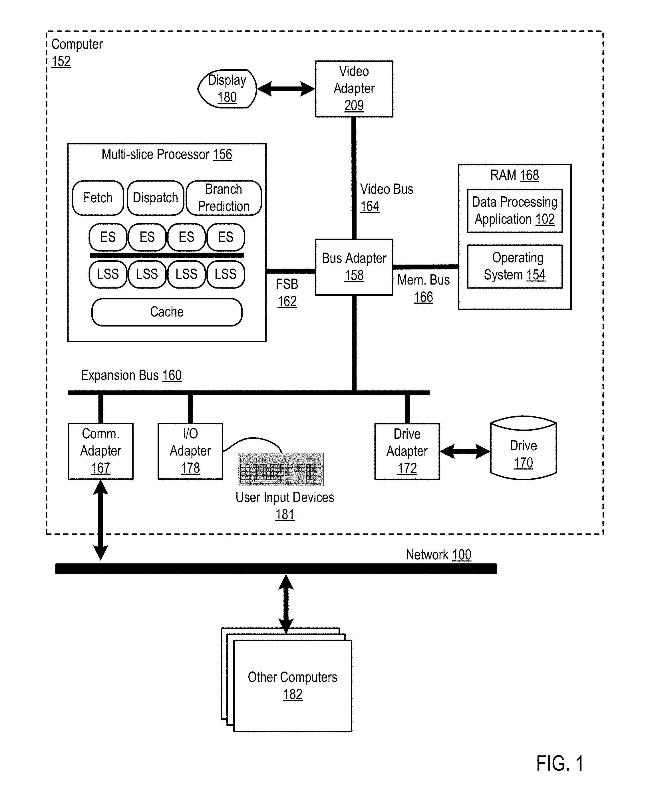
The computer (152) of FIG. 1 includes at least one computer processor (156) or `CPU` as well as random access memory (168) (`RAM`) which is connected through a high speed memory bus (166) and bus adapter (158) to processor (156) and to other components of the computer (152).
The example computer processor (156) of FIG. 1 may be implemented as a multi-slice processor. The term `multi-slice` as used in this specification refers to a processor having a plurality of similar or identical sets of components, where each set may operate independently of all the other sets or in concert with the one or more of the other sets. The multi-slice processor (156) of FIG. 1, for example, includes several execution slices (`ES`) and several load/store slices (`LSS`)--where load/store slices may generally be referred to as load/store units. Each execution slice may be configured to provide components that support execution of instructions: an issue queue, general purpose registers, a history buffer, an arithmetic logic unit (including a vector scalar unit, a floating point unit, and others), and the like. Each of the load/store slices may be configured with components that support data movement operations such as loading of data from cache or memory or storing data in cache or memory. In some embodiments, each of the load/store slices includes a data cache. The load/store slices are coupled to the execution slices through a results bus. In some embodiments, each execution slice may be associated with a single load/store slice to form a single processor slice. In some embodiments, multiple processor slices may be configured to operate together.
The example multi-slice processor (156) of FIG. 1 may also include, in addition to the execution and load/store slices, other processor components. In the system of FIG. 1, the multi-slice processor (156) includes fetch logic, dispatch logic, and branch prediction logic. Further, although in some embodiments each load/store slice includes cache memory, the multi-slice processor (156) may also include cache accessible by any or all of the processor slices.
Although the multi-slice processor (156) in the example of FIG. 1 is shown to be coupled to RAM (168) through a front side bus (162), a bus adapter (158) and a high speed memory bus (166), readers of skill in the art will recognize that such configuration is only an example implementation. In fact, the multi-slice processor (156) may be coupled to other components of a computer system in a variety of configurations. For example, the multi-slice processor (156) in some embodiments may include a memory controller configured for direct coupling to a memory bus (166). In some embodiments, the multi-slice processor (156) may support direct peripheral connections, such as PCIe connections and the like.
Stored in RAM (168) in the example computer (152) is a data processing application (102), a module of computer program instructions that when executed by the multi-slice processor (156) may provide any number of data processing tasks. Examples of such data processing applications may include a word processing application, a spreadsheet application, a database management application, a media library application, a web server application, and so on as will occur to readers of skill in the art. Also stored in RAM (168) is an operating system (154). Operating systems useful in computers configured for operation of a multi-slice processor according to embodiments of the present invention include UNIX.TM., Linux.TM., Microsoft Windows.TM., AIX.TM., IBM's z/OS.TM., and others as will occur to those of skill in the art. The operating system (154) and data processing application (102) in the example of FIG. 1 are shown in RAM (168), but many components of such software typically are stored in non-volatile memory also, such as, for example, on a disk drive (170).
The computer (152) of FIG. 1 includes disk drive adapter (172) coupled through expansion bus (160) and bus adapter (158) to processor (156) and other components of the computer (152). Disk drive adapter (172) connects non-volatile data storage to the computer (152) in the form of disk drive (170). Disk drive adapters useful in computers configured for operation of a multi-slice processor according to embodiments of the present invention include Integrated Drive Electronics (`IDE`) adapters, Small Computer System Interface (`SCSI`) adapters, and others as will occur to those of skill in the art. Non-volatile computer memory also may be implemented for as an optical disk drive, electrically erasable programmable read-only memory (so-called `EEPROM` or `Flash` memory), RAM drives, and so on, as will occur to those of skill in the art.
The example computer (152) of FIG. 1 includes one or more input/output (`I/O`) adapters (178). I/O adapters implement user-oriented input/output through, for example, software drivers and computer hardware for controlling output to display devices such as computer display screens, as well as user input from user input devices (181) such as keyboards and mice. The example computer (152) of FIG. 1 includes a video adapter (209), which is an example of an I/O adapter specially designed for graphic output to a display device (180) such as a display screen or computer monitor. Video adapter (209) is connected to processor (156) through a high speed video bus (164), bus adapter (158), and the front side bus (162), which is also a high speed bus.
The exemplary computer (152) of FIG. 1 includes a communications adapter (167) for data communications with other computers (182) and for data communications with a data communications network (100). Such data communications may be carried out serially through RS-232 connections, through external buses such as a Universal Serial Bus (`USB`), through data communications networks such as IP data communications networks, and in other ways as will occur to those of skill in the art. Communications adapters implement the hardware level of data communications through which one computer sends data communications to another computer, directly or through a data communications network. Examples of communications adapters useful in computers configured for operation of a multi-slice processor according to embodiments of the present invention include modems for wired dial-up communications, Ethernet (IEEE 802.3) adapters for wired data communications, and 802.11 adapters for wireless data communications.
The arrangement of computers and other devices making up the exemplary system illustrated in FIG. 1 are for explanation, not for limitation. Data processing systems useful according to various embodiments of the present invention may include additional servers, routers, other devices, and peer-to-peer architectures, not shown in FIG. 1, as will occur to those of skill in the art. Networks in such data processing systems may support many data communications protocols, including for example TCP (Transmission Control Protocol), IP (Internet Protocol), HTTP (HyperText Transfer Protocol), WAP (Wireless Access Protocol), HDTP (Handheld Device Transport Protocol), and others as will occur to those of skill in the art. Various embodiments of the present invention may be implemented on a variety of hardware platforms in addition to those illustrated in FIG. 1.
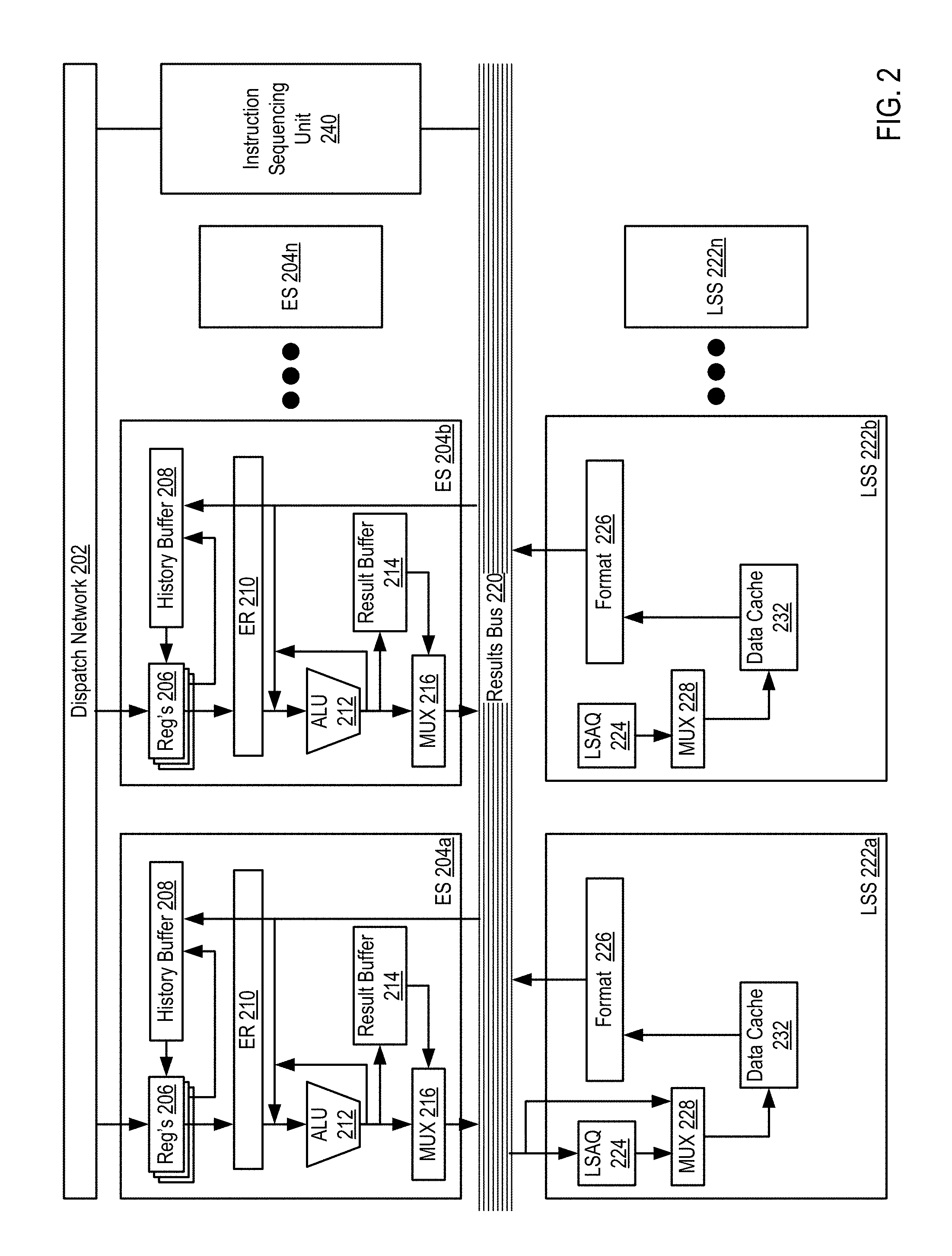
For further explanation, FIG. 2 sets forth a block diagram of a portion of a multi-slice processor according to embodiments of the present invention. The multi-slice processor in the example of FIG. 2 includes a dispatch network (202). The dispatch network (202) includes logic configured to dispatch instructions for execution among execution slices.
The multi-slice processor in the example of FIG. 2 also includes a number of execution slices (204a, 204b-204n). Each execution slice includes general purpose registers (206) and a history buffer (208). The general purpose registers and history buffer may sometimes be referred to as the mapping facility, as the registers are utilized for register renaming and support logical registers.
The general purpose registers (206) are configured to store the youngest instruction targeting a particular logical register and the result of the execution of the instruction. A logical register is an abstraction of a physical register that enables out-of-order execution of instructions that target the same physical register.
When a younger instruction targeting the same particular logical register is received, the entry in the general purpose register is moved to the history buffer, and the entry in the general purpose register is replaced by the younger instruction. The history buffer (208) may be configured to store many instructions targeting the same logical register. That is, the general purpose register is generally configured to store a single, youngest instruction for each logical register while the history buffer may store many, non-youngest instructions for each logical register.
Each execution slice (204) of the multi-slice processor of FIG. 2 also includes an execution reservation station (210). The execution reservation station (210) may be configured to issue instructions for execution. The execution reservation station (210) may include an issue queue. The issue queue may include an entry for each operand of an instruction. The execution reservation station may issue the operands for execution by an arithmetic logic unit or to a load/store slice (222a, 222b, 222c) via the results bus (220).
The arithmetic logic unit (212) depicted in the example of FIG. 2 may be composed of many components, such as add logic, multiply logic, floating point units, vector/scalar units, and so on. Once an arithmetic logic unit executes an operand, the result of the execution may be stored in the result buffer (214) or provided on the results bus (220) through a multiplexer (216).
The results bus (220) may be configured in a variety of manners and be of composed in a variety of sizes. In some instances, each execution slice may be configured to provide results on a single bus line of the results bus (220). In a similar manner, each load/store slice may be configured to provide results on a single bus line of the results bus (220). In such a configuration, a multi-slice processor with four processor slices may have a results bus with eight bus lines--four bus lines assigned to each of the four load/store slices and four bus lines assigned to each of the four execution slices. Each of the execution slices may be configured to snoop results on any of the bus lines of the results bus. In some embodiments, any instruction may be dispatched to a particular execution unit and then by issued to any other slice for performance. As such, any of the execution slices may be coupled to all of the bus lines to receive results from any other slice. Further, each load/store slice may be coupled to each bus line in order to receive an issue load/store instruction from any of the execution slices. Readers of skill in the art will recognize that many different configurations of the results bus may be implemented.
The multi-slice processor in the example of FIG. 2 also includes a number of load/store slices (222a, 222b-222n). Each load/store slice includes a queue (224), a multiplexer (228), a data cache (232), and formatting logic (226), among other components described below with regard to FIG. 3. The queue receives load and store operations to be carried out by the load/store slice (222). The formatting logic (226) formats data into a form that may be returned on the results bus (220) to an execution slice as a result of a load or store instruction.
The example multi-slice processor of FIG. 2 may be configured for flush and recovery operations. A flush and recovery operation is an operation in which the registers (general purpose register and history buffer) of the multi-slice processor are effectively `rolled back` to a previous state. The term `restore` and `recover` may be used, as context requires in this specification, as synonyms. Flush and recovery operations may be carried out for many reasons, including missed branch predictions, exceptions, and the like. Consider, as an example of a typical flush and recovery operation, that a dispatcher of the multi-slice processor dispatches over time and in the following order: an instruction A targeting logical register 5, an instruction B targeting logical register 5, and an instruction C targeting logical register 5. At the time instruction A is dispatched, the instruction parameters are stored in the general purpose register entry for logical register 5. Then, when instruction B is dispatched, instruction A is evicted to the history buffer (all instruction parameters are copied to the history buffer, including the logical register and the identification of instruction B as the evictor of instruction A), and the parameters of instruction B are stored in the general purpose register entry for logical register 5. When instruction C is dispatched, instruction B is evicted to the history buffer and the parameters of instruction C are stored in the general purpose register entry for logical register 5. Consider, now, that a flush and recovery operation of the registers is issued in which the dispatch issues a flush identifier matching the identifier of instruction C. In such an example, flush and recovery includes discarding the parameters of instruction C in the general purpose register entry for logical register 5 and moving the parameters of instruction B from the history buffer for instruction B back into the entry of general purpose register for logical register 5.
During the flush and recovery operation, in prior art processors, the dispatcher was configured to halt dispatch of new instructions to an execution slice. Such instructions may be considered either target or source instructions. A target instruction is an instruction that targets a logical register for storage of result data. A source instruction by contrast has, as its source, a logical register. A target instruction, when executed, will result in data stored in an entry of a register file while a source instruction utilizes such data as a source for executing the instruction. A source instruction, while utilizing one logical register as its source, may also target another logical register for storage of the results of instruction. That is, with respect to one logical register, an instruction may be considered a source instruction and with respect to another logical register, the same instruction may be considered a target instruction.
The multi-slice processor in the example of FIG. 2 also includes an instruction sequencing unit (240). While depicted as a single unit, each of the plurality of execution slices may include a respective instruction sequencing unit similar to instruction sequencing unit (240). Instruction sequencing unit (240) may take dispatched instructions and check dependencies of the instructions to determine whether all older instructions with respect to a current instruction have delivered, or may predictably soon deliver, results of these older instructions from which the current instruction is dependent so that the current instruction may execute correctly. If all dependencies to a current instruction are satisfied, then a current instruction may be determined to be ready to issue, and may consequently be issued--regardless of a program order of instructions as determined by an ITAG. Such issuance of instructions may be referred to as an "out-of-order" execution, and the multi-slice processor may be considered an out-of-order machine.
In some cases, a load/store unit receiving an issued instruction, such as a load/store slice, may not yet be able to handle the instruction, and the instruction sequencing unit (240) may keep the instruction queued until such time as the load/store slice may handle the instruction. After the instruction is issued, the instruction sequencing unit (240) may track progress of the instruction based at least in part on signals received from a load/store slice.
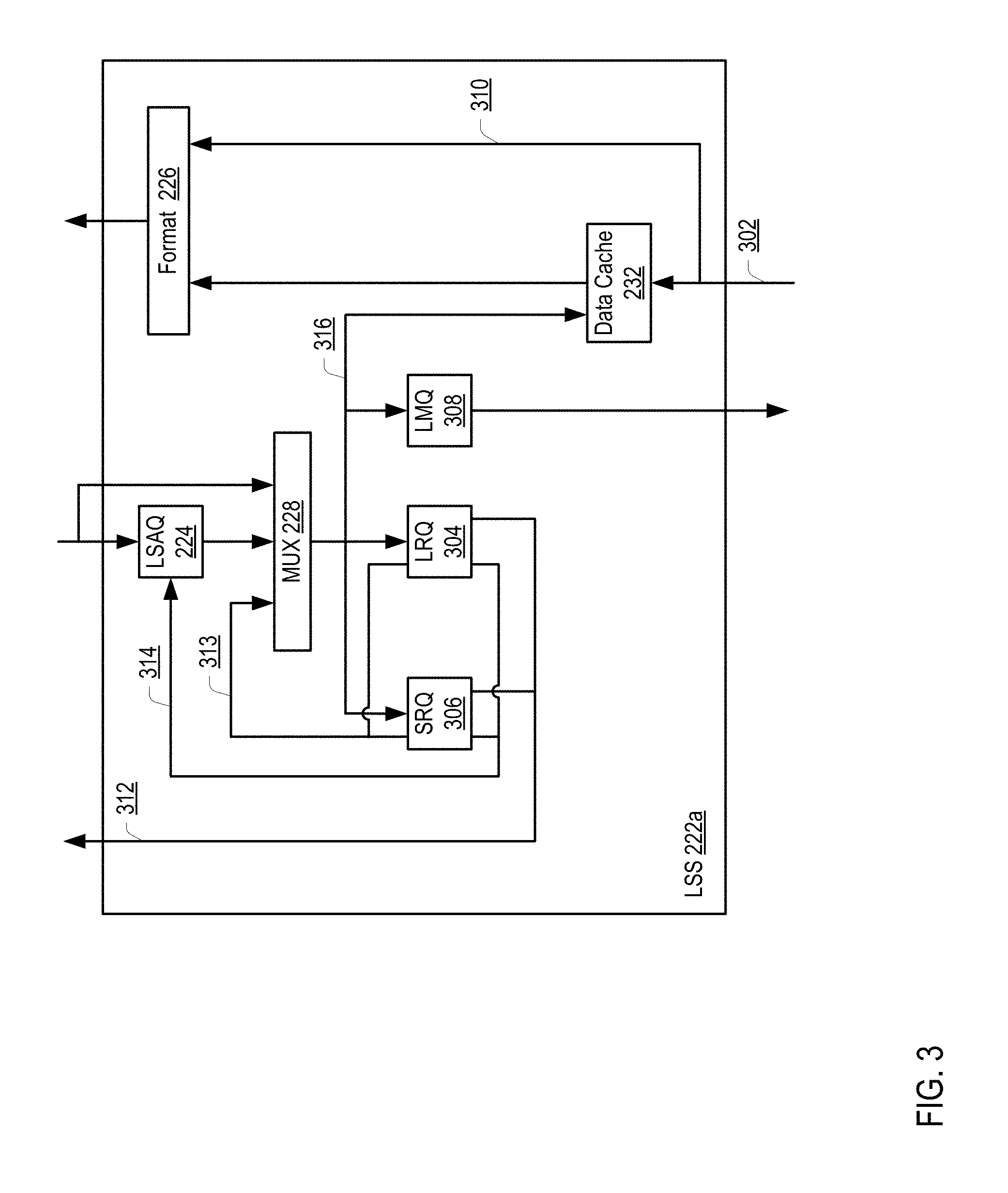
For further explanation, FIG. 3 sets forth a block diagram depicting an expanded view of a load/store slice (222a) implementing architectural components that include a load/store access queue (LSAQ) (224), a load reorder queue (LRQ) (304), a load miss queue (LMQ) (308), a store reorder queue (SRQ) (306), a data cache (232), among other components.
In previous systems, if a load/store unit received an instruction from an instruction sequencing unit, and the load/store unit was unable to handle the instruction for some reason, then the load/store unit would notify the instruction sequencing unit that the instruction was being rejected and the load/store unit would discard information related to the rejected instruction. In which case, the instruction sequencing unit would continue maintaining information to track and maintain the rejected instruction until the instruction is resent to the load/store unit. An instruction may be rejected for a variety of reasons, including an address miss in an address translation cache, a set prediction miss, data cache banking collisions, an overload of the load miss queue (308), among other possible rejection conditions.
The load/store slice (222a), by contrast to the above previous system, is configured to determine a rejection condition for an instruction received from an instruction sequencing unit, however, the load/store slice (222a), instead of sending a reject signal to the instruction sequencing unit, maintains tracking and handling of the instruction--including information usable to relaunch or reissue the instruction--until the rejection condition is resolved. Further, an entry in the load reorder queue (304) or the store reorder queue (306) may be configured to maintain information for tracking an instruction that would otherwise have been rejected and removed from the load reorder queue (304). For example, if the load/store slice (222a) determines that a rejection condition exists for a given load or store instruction, then logic within the load/store slice may notify the load reorder queue (304) or the store reorder queue (306) to place the instruction in a sleep state for a given number of cycles, or to place the instruction in a sleep state until notified to awaken, or to immediately reissue the instruction, among other notifications to perform other operations.
In this way, the load/store slice (222a) may save cycles that would otherwise be lost if the instruction were rejected to the instruction sequencing unit because the load/store slice (222a) may more efficiently and quickly reissue the instruction when the rejection condition is resolved in addition to more quickly detecting resolution of a rejection condition than an instruction sequencing unit. For example, if the load/store slice (222a) determines that an instruction that is in a sleep state may be reissued in response to determining that one or more rejection conditions have been resolved preventing the instruction from completing, then the load/store store slice may notify the load reorder queue (304) or the store reorder queue (306) to relaunch or reissue the instruction immediately or after some number of cycles. The number of cycles may depend upon a type of rejection condition or upon other factors affecting reissue or relaunch of the instruction. In this example, the load reorder queue (304) or the store reorder queue (306) may reissue or relaunch an instruction by providing the load/store access queue (224) with information to reissue the instruction, where the load reorder queue (304) or the store reorder queue (306) may communicate with the load/store access queue (224) along line (314) and may provide data for reissuing or relaunching the instruction along line (313).
Another improvement that results from the load/store slice (222a) maintaining an instruction if a rejection condition is determined is that the load/store slice (222a) uses fewer resources, such as logic and circuitry for latches and other components, to maintain the instruction than an instruction sequencing unit. In other words, given that the instruction sequencing unit may rely on the load/store slice (222a) in handling the instruction to completion, the instruction sequencing unit may free resources once the instruction is provided to the load/store slice (222a).
Further, the instruction sequencing unit (240), based at least in part on communications with the load/store slice (222a), may determine when and whether to wake instructions that may be dependent on a current instruction being handled by the load/store slice (222a). Therefore, if the load/store slice (222a) determines that a rejection condition exists, the load/store slice (222a) delays a notification to the instruction sequencing unit (240) to awaken dependent instructions to prevent the instruction sequencing unit (240) from issuing dependent instructions that are subsequently unable to finish due to lack of availability of results from a current instruction. In this way, the instruction sequencing unit (240) may avoid wasting execution cycles reissuing dependent instructions that are unable to finish.
For example, the load/store slice (222a) may communicate with the instruction sequencing unit (240) through the generation of signals indicating, at different points in handling a load instruction, that a load instruction is to be reissued or that data for a load instruction is valid. In some cases, in response to the instruction sequencing unit (240) receiving a signal from the load/store slice (222a) that a given instruction is to be reissued, the instruction sequencing unit (240) may awaken instructions dependent upon the given instruction with the expectation that the given instruction, after being reissued, is going to finish and provide valid data.
The load/store slice (222a) may also retrieve data from any tier of a memory hierarchy, beginning with a local data cache (232), and extending as far down in the hierarchy as needed to find requested data. The requested data, when received, may be provided to general purpose registers, virtual registers, or to some other destination. The received data may also be stored in a data cache (232) for subsequent access. The load/store slice (222a) may also manage translations of effective addresses to real addresses to communicate with different levels of memory hierarchy.
A store reorder queue (306) may include entries for tracking the cache operations for sequential consistency and may reissue operations into the load/store pipeline for execution independent of an execution slice.
A load miss queue (308) may issue requests for data to one or more data storage devices of a multi-tiered memory hierarchy, where a request for data may correspond to a load instruction for the data.
Responsive to the data being returned along the line (302) to the load/store slice (222a), the data may be delivered to a destination such as the results bus (220 of FIG. 2) to be loaded into, for example, a general purpose register--where the delivery of the data may be from the data cache (232) or over the line (310). The line (310) bypasses the data cache (232) and allows implementation of a critical data forwarding path. The load reorder queue (304) may also use line (312) to notify an instruction sequencing unit, or some other logical component, that the data is available.
A load reorder queue (304) may track execution of cache operations issued to the load/store slice (222a) and includes entries for tracking cache operations for sequential consistency, among other attributes. The load reorder queue (304) may also reissue operations into the load/store pipeline for execution, which provides operation that is independent of the execution slices.
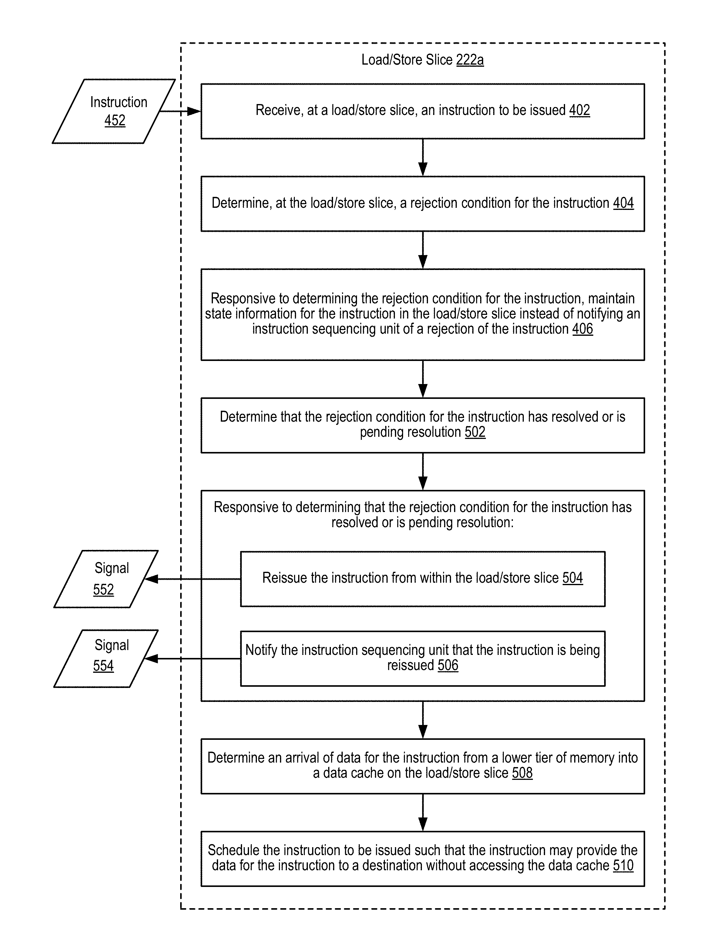
For further explanation, FIG. 4 sets forth a flow chart illustrating an exemplary method of operation of a multi-slice processor implementing a load/store unit configured to maintain rejected instructions. The method of FIG. 4 may be carried out by a multi-slice processor similar to that in the examples of FIGS. 1-3. Such a multi-slice processor may include an instruction sequencing unit (240), and a plurality of load/store slices (220a-220n), where each of the load/store slices may implement a load/store access queue (224), a load reorder queue (304), and a store reorder queue (306), as described above with regard to FIG. 3.
The method of FIG. 4 also includes receiving (402), at a load/store slice (222a), an instruction (452) to be issued. Receiving (402) the instruction may be carried out by the load/store slice (222a) receiving a request for the data at the load/store access queue (224), and moving the operation through the load/store slice (222a) pipeline. The instruction (452) may be received from the instruction sequencing unit (240), and the instruction (452) may be a load or store instruction.
During normal operation, a load operation may access data already stored in a data cache and the load operation finishes without being reissued. However, under some conditions, the load/store slice (222a) may determine that an instruction is to be reissued or rejected--where an instruction may be reissued immediately, or after some number of cycles dependent upon a rejection condition for the instruction being resolved. While it is often the case that a reissued instruction may complete, if a reissued instruction does not complete, sending a signal to the instruction sequencing unit (240) may result in instructions dependent upon the reissued instruction being awakened prematurely. Similarly, under some conditions, a store instruction may be unable to be performed.
The method of FIG. 4 also includes determining (404), at the load/store slice (224a), a rejection condition for the instruction (452). Determining (404) a rejection condition for the instruction (452) may be carried out by load/store slice (222a) determining one or more conditions that would cause the load/store slice (222a) to reject the instruction, including the data cache being unable to currently read a requested data address, a translation mechanism being unable to translate the requested data address, a load/miss queue being too busy to handle the instruction request, a detected hazard with other load or store instructions, waiting for a store forward to complete, among other possible conditions for rejecting an instruction.
The method of FIG. 4 also includes, responsive to determining, at the load/store slice (222a), a rejection condition for the instruction, maintaining (406) state information for the instruction in the load/store slice (222a) instead of notifying an instruction sequencing unit of a rejection of the instruction. Maintaining (406) state information for the instruction in the load/store slice (222a) may be carried out by logic within the load/store slice (222a) notifying in the case of a load instruction--the load reorder queue (304) to modify status for an entry storing state information to indicate a sleep state or a state that would otherwise idle the instruction. Similarly, in the case that the instruction is a store instruction, the logic within the load/store slice (222a) may notify the store reorder queue (306) to modify status for an entry storing state information to indicate a sleep state or a state that would otherwise idle the instruction.
Further, maintaining the state information may include storing, for example, within an entry of the load reorder queue (304) or store reorder queue (306), information that may be used to reissue or relaunch the instruction after a notification is received to awaken due to a rejection condition being resolved, or due to a rejection condition being expected to resolve within a quantity of cycles.
For example, an entry may store, or maintain, information previously held to handle instructions so that a reissued instruction appears identical or similar to the instruction as originally received from an instruction sequencing unit. For example, an entry may store, or maintain, instruction operation codes, or opcodes, effective address information to determine which bytes in a cacheline are involved in an instruction, an ITAG, which may be used for ordering instructions, a real address, which may describe a cacheline address used by lower tiers of memory, and various control bits, among other information. Further, the entry may store, or maintain, a set of wait states corresponding to different rejection conditions, where this information may be a basis for awakening instructions in response to corresponding rejection conditions being resolved.
The load reorder queue (304) and the store reorder queue (306) are further configured to, in response to being notified to place an instruction into a sleep state, not send any signal or notification to the instruction sequencing unit that provided the instruction to prevent the instruction sequencing unit from prematurely awakening any instructions dependent on the instruction being placed into a sleep state.
For example, in response to the instruction sequencing unit (240) receiving a signal on the results bus (220) indicating that an instruction is being reissued, the instruction sequencing unit (240) may awaken instructions dependent on the reissued instruction in anticipation that a data valid signal is to follow, which would allow the dependent instructions to execute properly. However, if the load/store slice (222a) delays sending a signal that an instruction is being reissued, the instruction sequencing unit (240) does not awaken instructions dependent upon the reissued instruction, thereby avoiding cancelation of dependent instructions awakened for a reissued instruction that does not complete upon reissue, which prevents wasting execution cycles recovering from canceling the dependent instructions.
In this way, the load/store slice (222a) relieves the instruction sequencing unit from expending any resources tracking an instruction once the instruction sequencing unit provides the instruction to the load/store slice (222a) because the instruction sequencing unit relies on the load/store slice (222a) to handle the instruction to completion whether or not the load/store slice (222a) determines or identifies any rejection conditions that would have otherwise required the instruction sequencing unit to maintain status information for the instruction.
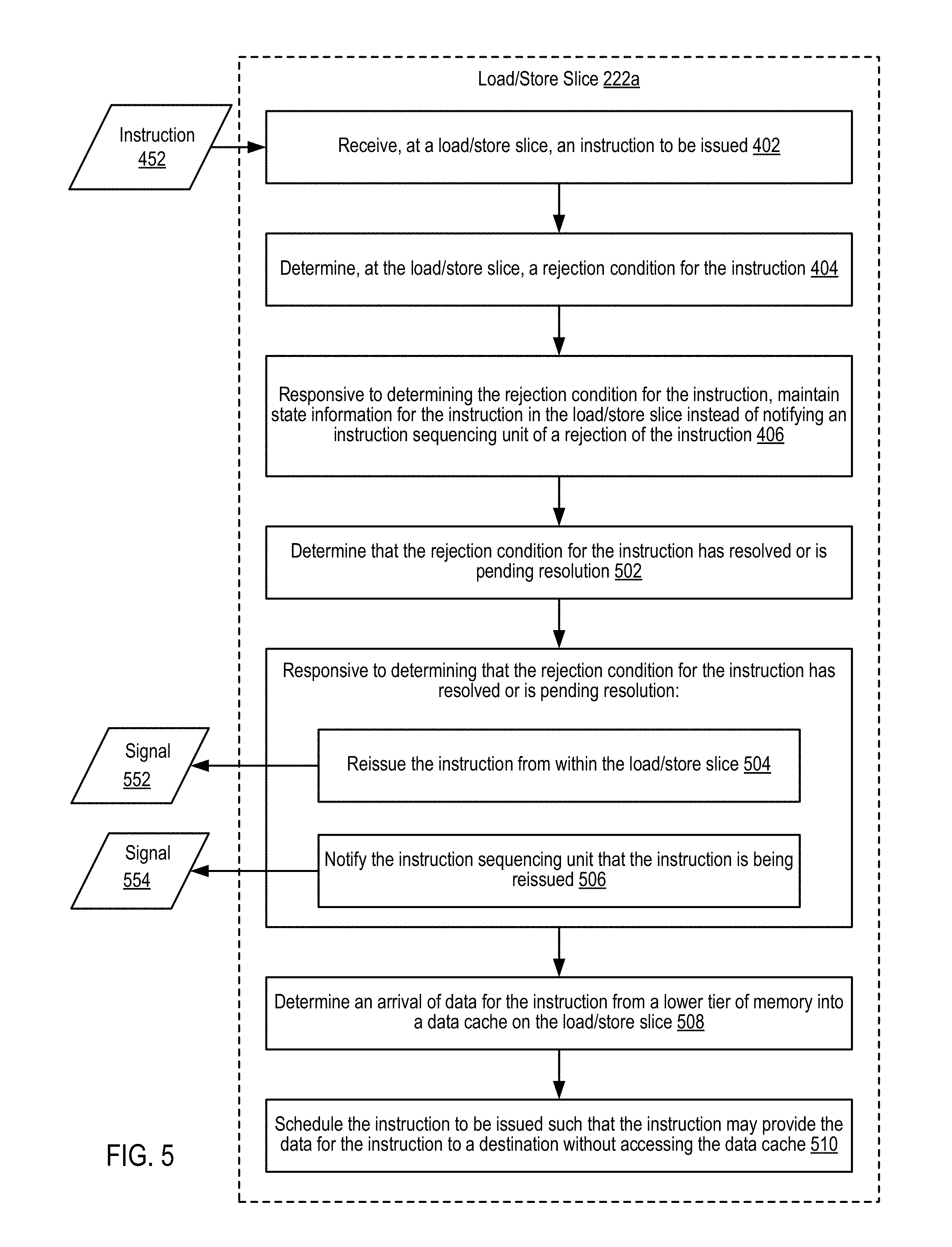
For further explanation, FIG. 5 sets forth a flow chart illustrating an exemplary method of operation of a multi-slice processor implementing a load/store unit configured to maintain rejected instructions. The method of FIG. 5 may be carried out by a multi-slice processor similar to that in the examples of FIGS. 1-3. Such a multi-slice processor may include an instruction sequencing unit (240), and a plurality of load/store slices (220a-220n), where each of the load/store slices may implement a load/store access queue (224), a load reorder queue (304), and a store reorder queue (306), as described above with regard to FIG. 3.
The method of FIG. 5 is similar to the method of FIG. 4 in that the method of FIG. 5 also includes receiving (402), at a load/store slice (222a), an instruction (452) to be issued; determining (404), at the load/store slice (224a), a rejection condition for the instruction (452); and responsive to determining, at the load/store slice (222a), a rejection condition for the instruction, maintaining (406) state information for the instruction in the load/store slice (222a) instead of notifying an instruction sequencing unit of a rejection of the instruction.
The method of FIG. 5 differs from the method of FIG. 4, however, in that the method of FIG. 5 further includes: determining (502) that the rejection condition for the instruction has resolved or is pending resolution; responsive to determining that the rejection condition for the instruction has resolved or is pending resolution, reissuing (504) the instruction from within the load/store slice (222a) and notifying (506) the instruction sequencing unit that the instruction is being reissued; determining (508) an arrival of data for the instruction from a lower tier of memory into the data cache (232) on the load/store slice (222a); and scheduling (510) the instruction to be issued such that the instruction may provide the data for the instruction to a destination without accessing the data cache (232).
Determining (502) that the rejection condition for the instruction has resolved or is pending resolution may be carried out by the load/store slice (222a) determining that one or more of the conditions on which a rejection of the instruction may be based, as determined at (404), has been resolved or is expected to be resolved within some quantity of cycles. For example, the load/store slice (222a) may determine resolution of rejection conditions including: the data cache being unable to currently read a requested data address, a translation mechanism being unable to translate the requested data address, a load/miss queue being too busy to handle the instruction request, a detected hazard with other load or store instructions, waiting for a store forward to complete, among other possible conditions for rejecting an instruction.
The load/store slice (222a) may further determine, based on a type of rejection, a quantity of cycles within which a resolution of a rejection condition is expected to resolve, and notify the load reorder queue (304) or the store reorder queue (306).
Reissuing (504) the instruction (452) from within the load/store slice (222a) may be carried out by the load/store slice (222a) notifying either the load reorder queue (304) or the store reorder queue (306) to awaken an instruction previously placed in a sleep state or to awaken after passage, the lapse of, a quantity of cycles. In response to receiving a signal to awaken, the load reorder queue (304) or the store reorder queue (306) may signal (552) the load/store access queue (224) along line (314) to reissue or relaunch an instruction.
Further, the load/store slice (222a) may determine an order in which to awaken multiple instructions that are in a sleep state awaiting resolution of rejection conditions. In other words, while instructions arrive at the load/store slice (222a) in an order determined by an instruction sequencing unit, the load/store slice (222a) may reorder instructions such that any effect of the completed, reordered instructions, is consistent with the order in which the instructions were received from the instruction sequencing unit. For example, the load/store slice (222a) may determine awakening priorities based on at least in part on an age of an instruction, a measure of nearness to completion for the instruction, or according to an instruction that may take advantage of carry data forwarding.
Notifying (506) the instruction sequencing unit (240) that the instruction is being reissued may be carried out by the load reorder queue (304) or the store reorder queue (306) generating a signal (554) notifying the instruction sequencing unit (240) along line (312) to the results bus (220)--where the signal (554) may indicate to the instruction sequencing unit (240) an identification of a reissue signal, and an ITAG identifying the instruction being reissued.
Further, the load/store slice (222a) may propagate a signal to the instruction sequencing unit (240) indicating that the data requested by the load instruction, identifiable by an ITAG, is on a results bus and is valid, where the instruction sequencing unit (240) receives the signal and corresponds the signal with an indication that the data is valid and on the results bus (220).
Determining (508) an arrival of data for the instruction from a lower tier of memory into the data cache (232) on the load/store slice (222a) may be carried out by the load/store slice (222a) receiving an indication from a lower tier of memory that requested data is moving toward the data cache (232) and may be expected to be available at a given number of cycles. Such information may allow the load/store slice (222a) to awaken load instructions in time to make use of a carry data forward path.
Scheduling (510) the instruction to be issued such that the instruction may provide the data for the instruction to a destination without accessing the data cache (232) may be carried out by the load/store slice (222a) notifying the load reorder queue (304) to awaken a sleeping instruction in time so that the instruction may provide the data being received to a destination along a carry data forward path (310) without waiting for the requested data first being latched or stored in the data cache (232). In other words, the instruction makes use of the carry data forwarding technique described above with regard to FIG. 3. For example, the load/store slice (222a) may determine how many cycles from a current point to wait before sending an awaken signal to the load reorder queue (304) so that when the awakened instruction has progressed through reissue to make use of the requested data, the data is available.
In this way, the load/store slice (222a) may awaken instructions at points in time a number of cycles from a current point so that the awakened and reissued instructions are not delayed in completing.
For further explanation, FIG. 6 sets forth a flow chart illustrating an exemplary method of operation of a multi-slice processor implementing a load/store unit configured to maintain rejected instructions. The method of FIG. 6 may be carried out by a multi-slice processor similar to that in the examples of FIGS. 1-3. Such a multi-slice processor may include an instruction sequencing unit (240), and a plurality of load/store slices (220a-220n), where each of the load/store slices may implement a load/store access queue (224), a load reorder queue (304), and a store reorder queue (306), as described above with regard to FIG. 3.
The method of FIG. 6 is similar to the method of FIG. 4 in that the method of FIG. 6 also includes receiving (402), at a load/store slice (222a), a load instruction (452) to be issued; determining (404), at the load/store slice (224a), a rejection condition for the instruction (452); and responsive to determining, at the load/store slice (222a), a rejection condition for the instruction, maintaining (406) state information for the instruction in the load/store slice (222a) instead of notifying an instruction sequencing unit of a rejection of the instruction.
The method of FIG. 6 differs from the method of FIG. 4, however, in that the method of FIG. 5 further includes determining (602) if the instruction (452) is a load or a store, where if the instruction (452) is a load, then providing (604), from the load/store access queue (224) to the load reorder queue (304), the instruction, and if the instruction (452) is a store, then providing (606), from the load/store access queue (224) to the store reorder queue (306).
Determining (602) if the instruction (452) is a load or a store may be carried out by the load/store slice (222a) determining whether an opcode for the instruction (452) received from the instruction sequencing unit matches a load operation or a store operation.
Providing (604), from the load/store access queue (224) to the load reorder queue (304), the instruction (452) may be carried out by the load/store access queue (224) propagating the instruction (452) through MUX (228) along line (316) to the load reorder queue (304).
Providing (606), from the load/store access queue (224) to the store reorder queue (304), the instruction (452) may be carried out by the load/store access queue (224) propagating the instruction (452) through MUX (228) along line (316) to the store reorder queue (306).
In this way, the load/store access queue (224) may route load and store instructions to corresponding queues for handling the instruction, where both the load reorder queue (304) and the store reorder queue (306) include entries that are configured to maintain information for maintaining instructions that are determined to be subject to rejection conditions such that the maintained information may be used to reawaken and reissue the instructions pending resolution of one or more rejection conditions.
The present invention may be a system, a method, and/or a computer program product. The computer program product may include a computer readable storage medium (or media) having computer readable program instructions thereon for causing a processor to carry out aspects of the present invention.
The computer readable storage medium can be a tangible device that can retain and store instructions for use by an instruction execution device. The computer readable storage medium may be, for example, but is not limited to, an electronic storage device, a magnetic storage device, an optical storage device, an electromagnetic storage device, a semiconductor storage device, or any suitable combination of the foregoing. A non-exhaustive list of more specific examples of the computer readable storage medium includes the following: a portable computer diskette, a hard disk, a random access memory (RAM), a read-only memory (ROM), an erasable programmable read-only memory (EPROM or Flash memory), a static random access memory (SRAM), a portable compact disc read-only memory (CD-ROM), a digital versatile disk (DVD), a memory stick, a floppy disk, a mechanically encoded device such as punch-cards or raised structures in a groove having instructions recorded thereon, and any suitable combination of the foregoing. A computer readable storage medium, as used herein, is not to be construed as being transitory signals per se, such as radio waves or other freely propagating electromagnetic waves, electromagnetic waves propagating through a waveguide or other transmission media (e.g., light pulses passing through a fiber-optic cable), or electrical signals transmitted through a wire.
Computer readable program instructions described herein can be downloaded to respective computing/processing devices from a computer readable storage medium or to an external computer or external storage device via a network, for example, the Internet, a local area network, a wide area network and/or a wireless network. The network may comprise copper transmission cables, optical transmission fibers, wireless transmission, routers, firewalls, switches, gateway computers and/or edge servers. A network adapter card or network interface in each computing/processing device receives computer readable program instructions from the network and forwards the computer readable program instructions for storage in a computer readable storage medium within the respective computing/processing device.
Computer readable program instructions for carrying out operations of the present invention may be assembler instructions, instruction-set-architecture (ISA) instructions, machine instructions, machine dependent instructions, microcode, firmware instructions, state-setting data, or either source code or object code written in any combination of one or more programming languages, including an object oriented programming language such as Smalltalk, C++ or the like, and conventional procedural programming languages, such as the "C" programming language or similar programming languages. The computer readable program instructions may execute entirely on the user's computer, partly on the user's computer, as a stand-alone software package, partly on the user's computer and partly on a remote computer or entirely on the remote computer or server. In the latter scenario, the remote computer may be connected to the user's computer through any type of network, including a local area network (LAN) or a wide area network (WAN), or the connection may be made to an external computer (for example, through the Internet using an Internet Service Provider). In some embodiments, electronic circuitry including, for example, programmable logic circuitry, field-programmable gate arrays (FPGA), or programmable logic arrays (PLA) may execute the computer readable program instructions by utilizing state information of the computer readable program instructions to personalize the electronic circuitry, in order to perform aspects of the present invention.
Aspects of the present invention are described herein with reference to flowchart illustrations and/or block diagrams of methods, apparatus (systems), and computer program products according to embodiments of the invention. It will be understood that each block of the flowchart illustrations and/or block diagrams, and combinations of blocks in the flowchart illustrations and/or block diagrams, can be implemented by computer readable program instructions.
These computer readable program instructions may be provided to a processor of a general purpose computer, special purpose computer, or other programmable data processing apparatus to produce a machine, such that the instructions, which execute via the processor of the computer or other programmable data processing apparatus, create means for implementing the functions/acts specified in the flowchart and/or block diagram block or blocks. These computer readable program instructions may also be stored in a computer readable storage medium that can direct a computer, a programmable data processing apparatus, and/or other devices to function in a particular manner, such that the computer readable storage medium having instructions stored therein comprises an article of manufacture including instructions which implement aspects of the function/act specified in the flowchart and/or block diagram block or blocks.
The computer readable program instructions may also be loaded onto a computer, other programmable data processing apparatus, or other device to cause a series of operational steps to be performed on the computer, other programmable apparatus or other device to produce a computer implemented process, such that the instructions which execute on the computer, other programmable apparatus, or other device implement the functions/acts specified in the flowchart and/or block diagram block or blocks.
The flowchart and block diagrams in the Figures illustrate the architecture, functionality, and operation of possible implementations of systems, methods, and computer program products according to various embodiments of the present invention. In this regard, each block in the flowchart or block diagrams may represent a module, segment, or portion of instructions, which comprises one or more executable instructions for implementing the specified logical function(s). In some alternative implementations, the functions noted in the block may occur out of the order noted in the figures. For example, two blocks shown in succession may, in fact, be executed substantially concurrently, or the blocks may sometimes be executed in the reverse order, depending upon the functionality involved. It will also be noted that each block of the block diagrams and/or flowchart illustration, and combinations of blocks in the block diagrams and/or flowchart illustration, can be implemented by special purpose hardware-based systems that perform the specified functions or acts or carry out combinations of special purpose hardware and computer instructions.
It will be understood from the foregoing description that modifications and changes may be made in various embodiments of the present invention without departing from its true spirit. The descriptions in this specification are for purposes of illustration only and are not to be construed in a limiting sense. The scope of the present invention is limited only by the language of the following claims.
* * * * *
References
-
ip.com/IPCOM/000224167
-
-
-
-
-
repository.upenn.edu/cis_papers/262
-
-
priorart.ip.com/IPCOM/000249317
-
-
google.com/&httpsredir=1&article=1023&context=cis_reports
D00000
D00001
D00002
D00003
D00004
D00005
D00006
XML
uspto.report is an independent third-party trademark research tool that is not affiliated, endorsed, or sponsored by the United States Patent and Trademark Office (USPTO) or any other governmental organization. The information provided by uspto.report is based on publicly available data at the time of writing and is intended for informational purposes only.
While we strive to provide accurate and up-to-date information, we do not guarantee the accuracy, completeness, reliability, or suitability of the information displayed on this site. The use of this site is at your own risk. Any reliance you place on such information is therefore strictly at your own risk.
All official trademark data, including owner information, should be verified by visiting the official USPTO website at www.uspto.gov. This site is not intended to replace professional legal advice and should not be used as a substitute for consulting with a legal professional who is knowledgeable about trademark law.