Method Of Topology-selective Film Formation Of Silicon Oxide
Fukazawa; Atsuki ; et al.
U.S. patent application number 17/068495 was filed with the patent office on 2021-04-22 for method of topology-selective film formation of silicon oxide. The applicant listed for this patent is ASM IP Holding B.V.. Invention is credited to Pei-Chia Chen, Atsuki Fukazawa, Masaru Zaitsu.
| Application Number | 20210118667 17/068495 |
| Document ID | / |
| Family ID | 1000005211387 |
| Filed Date | 2021-04-22 |


| United States Patent Application | 20210118667 |
| Kind Code | A1 |
| Fukazawa; Atsuki ; et al. | April 22, 2021 |
METHOD OF TOPOLOGY-SELECTIVE FILM FORMATION OF SILICON OXIDE
Abstract
A method for forming a silicon oxide film on a step formed on a substrate includes: (a) designing a topology of a final silicon oxide film by preselecting a target portion of an initial silicon nitride film to be selectively deposited or removed or reformed with reference to a non-target portion of the initial silicon nitride film resulting in the final silicon oxide film; and (b) forming the initial silicon nitride film and the final silicon oxide film on the surfaces of the step according to the topology designed in process (a), wherein the initial silicon nitride film is deposited by ALD using a silicon-containing precursor containing halogen, and the initial silicon nitride film is converted to the final silicon oxide film by oxidizing the initial silicon nitride film without further depositing a film wherein a Si--N bond in the initial silicon nitride film is converted to a Si--O bond.
| Inventors: | Fukazawa; Atsuki; (Tokyo, JP) ; Zaitsu; Masaru; (Kawasaki-shi, JP) ; Chen; Pei-Chia; (Tokyo, JP) | ||||||||||
| Applicant: |
|
||||||||||
|---|---|---|---|---|---|---|---|---|---|---|---|
| Family ID: | 1000005211387 | ||||||||||
| Appl. No.: | 17/068495 | ||||||||||
| Filed: | October 12, 2020 |
Related U.S. Patent Documents
| Application Number | Filing Date | Patent Number | ||
|---|---|---|---|---|
| 62916226 | Oct 16, 2019 | |||
| Current U.S. Class: | 1/1 |
| Current CPC Class: | H01L 21/0228 20130101; H01L 21/02249 20130101; H01L 21/0217 20130101; C23C 16/45525 20130101; C23C 16/345 20130101; H01L 21/31111 20130101; H01L 21/02274 20130101; H01L 21/0223 20130101; C23C 16/56 20130101; H01L 21/02252 20130101; H01L 21/02164 20130101 |
| International Class: | H01L 21/02 20060101 H01L021/02; H01L 21/311 20060101 H01L021/311; C23C 16/34 20060101 C23C016/34; C23C 16/455 20060101 C23C016/455; C23C 16/56 20060101 C23C016/56 |
Claims
1. A method for forming a silicon oxide film on a step having a top surface, a sidewall, and a bottom surface formed on a substrate, comprising processes of: (a) designing a topology of a final silicon oxide film, which is a conformal film or a film having low conformality, formed on the step by preselecting a target portion of an initial silicon nitride film to be selectively deposited or removed or reformed with reference to a non-target portion of the initial silicon nitride film resulting in the final silicon oxide film, said selectively deposited target portion being a top/bottom portion of the initial silicon nitride film formed on the top and bottom surfaces of the step, said selectively removed or reformed target portion being a sidewall portion of the initial silicon nitride film formed on the sidewall of the step; and (b) forming the initial silicon nitride film and the final silicon oxide film on the surfaces of the step according to the topology designed in process (a), wherein the initial silicon nitride film is deposited by atomic layer deposition (ALD) using a silicon-containing precursor containing halogen, and the initial silicon nitride film is converted to the final silicon oxide film by oxidizing the initial silicon nitride film without further depositing a film wherein a Si--N bond in the initial silicon nitride film is converted to a Si--O bond.
2. The method according to claim 1, wherein the precursor used in process (b) contains no carbon, and the final silicon oxide film is free of carbon.
3. The method according to claim 1, wherein the formation of the initial silicon nitride film and the oxidization of the initial silicon nitride film are continuously conducted in process (b) in a same reaction space.
4. The method according to claim 3, wherein the reaction space is purged after the formation of the initial silicon nitride film before the oxidization of the initial silicon nitride film, and the oxidization of the initial silicon nitride film is plasma oxidization conducted in the reaction space into which an oxidizing gas is introduced, which is at least one gas selected from the group consisting of O.sub.2, O.sub.3, CO.sub.2, N.sub.2O, and H.sub.2O.
5. The method according to claim 1, wherein the initial silicon nitride film is composed of multiple monolayers and, in process (b), the oxidization of the initial silicon nitride film is conducted after each monolayer deposition cycle of ALD of the initial silicon nitride film or after every multiple monolayer deposition cycles of ALD of the initial silicon nitride film.
6. The method according to claim 1, wherein the target portion preselected in process (a) is the selectively deposited target portion, wherein process (b) comprises: (ci) depositing a silicon oxide film on the surfaces of the step on the substrate; (cii) anisotropically nitriding a surface of the silicon oxide film using a nitrogen-hydrogen-containing plasma generated by applying RF power between two electrodes between which the substrate is placed in parallel to the two electrodes, in a manner nitriding the surface of the silicon oxide film predominantly on the top and bottom surfaces of the step, rather than on the sidewall of the step, thereby introducing --NH terminals on the surface of the silicon oxide film; (ciii) depositing, on and in contact with the surface-treated silicon oxide film, at least part of the initial silicon nitride film by ALD using the precursor and a nitriding gas excited by a plasma generated by applying RF power between the two electrodes; (civ) oxidizing the at least part of the initial silicon nitride film using an excited oxidizing gas to obtain at least part of the final silicon oxide film without further depositing a film wherein a Si--N bond in the initial silicon nitride film is converted to a Si--O bond; and (cv) as necessary, repeating processes (cii) and (civ) until the final silicon oxide film having a desired thickness is obtained.
7. The method according to claim 6, wherein the nitrogen-hydrogen-containing plasma in process (cii) is generated using a mixture of N.sub.2 and H.sub.2, NH.sub.3, other N.sub.xH.sub.y wherein x and y are integers, or a mixture of two or more of the foregoing.
8. The method according to claim 6, wherein the silicon oxide film in process (ci) is deposited by ALD or CVD.
9. The method according to claim 1, wherein the target portion preselected in process (a) is the selectively removed target portion, wherein process (b) comprises: (di) depositing at least part of the initial silicon nitride film on the surfaces of the step on the substrate by ALD using the precursor and a reactant gas excited by a plasma generated by applying RF power between two electrodes between which the substrate is placed in parallel to the two electrodes, wherein RF power is applied at 0.14 W/cm.sup.2 to 1.41 W/cm.sup.2 per area of the substrate for five seconds or less in each monolayer deposition cycle of ALD, thereby giving the target portion lower chemical resistance properties than those of the non-target portion when subjected to wet-etching; (dii) oxidizing the at least part of the initial silicon nitride film using an excited oxidizing gas to obtain at least part of an intermediate silicon oxide film without further depositing a film wherein a Si--N bond in the initial silicon nitride film is converted to a Si--O bond; and (diii) as necessary, repeating processes (di) and (dii) until the intermediate silicon oxide film having a desired thickness is obtained; and then (div) wet-etching the intermediate silicon oxide film to obtain the final dielectric film, thereby removing predominantly the target portion with reference to the non-target portion.
10. The method according to claim 9, wherein the oxidization in process (dii) is conducted using plasma, UV light, heat, or a combination of two or more of the foregoing.
11. The method according to claim 9, wherein RF power used in process (di) is 0.14 W/cm.sup.2 to 0.71 W/cm.sup.2 per area of the substrate, and the oxidization in process (dii) is plasma oxidization conducted after each monolayer deposition cycle of ALD of the initial silicon nitride film or after every multiple monolayer deposition cycles of AD of the initial silicon nitride film in process (di), wherein the plasma is generated by applying RF power at 0.07 W/cm.sup.2 to 0.71 W/cm.sup.2 per area of the substrate between two electrodes between which the substrate is placed in parallel to the two electrodes.
12. The method according to claim 9, wherein process (diii) is conducted wherein immediately before repeating process (di) each time, surfaces of the step of the substrate are exposed to a hydrogen-containing reducing gas to treat the surfaces with the hydrogen-containing reducing gas.
13. The method according to claim 12, wherein the hydrogen-containing reducing gas is at least one gas selected from the group consisting of H.sub.2 and NH.sub.3.
14. The method according to claim 9, wherein in process (div), the wet-etching is wet-etching using dHF.
15. The method according to claim 1, wherein the target portion preselected in process (a) is the selectively reformed target portion, wherein process (b) comprises: (ei) depositing at least part of the initial silicon nitride film on the surfaces of the step on the substrate by ALD using the precursor and a reactant gas excited by a plasma generated by applying RF power between two electrodes between which the substrate is placed in parallel to the two electrodes, wherein RF power is applied at 0.14 W/cm.sup.2 to 1.41 W/cm.sup.2 per area of the substrate for more than five seconds in each monolayer deposition cycle of ALD, thereby giving the target portion chemical resistance properties substantially equal to those of the non-target portion when subjected to wet-etching; (eii) oxidizing the at least part of the initial silicon nitride film using an excited oxidizing gas to obtain at least part of an intermediate silicon oxide film without further depositing a film wherein a Si--N bond in the initial silicon nitride film is converted to a Si--O bond; and (eiii) as necessary repeating processes (ei) and (eii) until the intermediate silicon oxide film having a desired thickness is obtained, wherein the intermediate silicon oxide film is regarded as the final silicon oxide film having high conformality if optional process (eiv) is not conducted; and then (eiv) optionally wet-etching the intermediate silicon oxide film to adjust conformality of the intermediate silicon oxide film to obtain the final dielectric film, thereby forming the final silicon oxide film having high conformality.
16. The method according to claim 15, wherein the oxidization in process (eii) is conducted using plasma, UV light, heat, or a combination of two or more of the foregoing.
17. The method according to claim 15, wherein RF power used in process (ei) is 0.71 W/cm.sup.2 to 1.41 W/cm.sup.2 per area of the substrate, and the oxidization in process (eii) is plasma oxidization conducted after each monolayer deposition cycle of ALD of the initial silicon nitride film or after every multiple monolayer deposition cycles of AD of the initial silicon nitride film in process (ei), wherein the plasma is generated by applying RF power at 0.07 W/cm.sup.2 to 0.71 W/cm.sup.2 per area of the substrate between two electrodes between which the substrate is placed in parallel to the two electrodes.
18. The method according to claim 15, wherein process (eiii) is conducted wherein immediately before repeating process (ei) each time, surfaces of the step of the substrate are exposed to a hydrogen-containing reducing gas to treat the surfaces with the hydrogen-containing reducing gas.
19. The method according to claim 18, wherein the hydrogen-containing reducing gas is at least one gas selected from the group consisting of H.sub.2 and NH.sub.3.
20. The method according to claim 15, wherein in process (eiv), the wet-etching is wet-etching using dHF.
Description
CROSS-REFERENCE TO RELATED APPLICATIONS
[0001] This application claims the benefit of U.S. Provisional Application No. 62/916,226, filed on Oct. 16, 2019, in the United States Patent and Trademark Office, the disclosure of which is incorporated herein in its entirety by reference.
BACKGROUND
Field of the Invention
[0002] The present invention relates generally to a method for forming a silicon oxide film on a step having a top surface, a sidewall, and a bottom surface formed on a substrate, particularly, a method of topology-selective film formation of silicon oxide.
Related Art
[0003] Atomic layer deposition (ALD) methods including a plasma-enhanced atomic layer deposition (PEALD) method are widely used in semiconductor-manufacturing processes as a method of forming a conformal film on a substrate having a patterned surface. In some semiconductor-manufacturing processes, a film which has been formed once as a conformal film is subjected to dry etching or other dry trimming processes in order to anisotropically remove a part or parts of the film for particular applications. In that case, a film formation process and an etching process are conducted necessarily in two separate steps.
[0004] However, when a thin film is subjected to etching, etching selectivity of the thin film, an underlying film, and a mask material, i.e., a degree of differences in resistance to etching among the thin film, the underlying film, and the mask material, is always an issue, and adverse effect on the underlying film (e.g., degradation of the quality of the underlying film by penetrated ion energy, and degradation of critical dimensions (CD) of a trench), for example, is inevitable.
[0005] If film formation itself can control a topology of the film by anisotropic deposition and/or anisotropic reforming process, no dry etching or other dry trimming processes are required so as to eliminate adverse effect on the underlying film by dry etching, reduce the number of process steps, and increase a throughput. However, controlling a topology of silicon oxide film is very difficult because oxidation occurs rather isotropically in a film deposition process.
[0006] As such technology of controlling a topology of film, it is known that first a SiN film is deposited on a patterned surface of a substrate under certain conditions such that a wet etch rate of a horizontal portion and that of a vertical portion of the pattern are different, followed by wet etching, thereby leaving selectively only either a sidewall portion of the pattern or a horizontal portion of the pattern (as disclosed in e.g., U.S. Patent Publication No. 2017/0243734, the disclosure of which is incorporated by reference in its entirety as applicable to certain embodiments disclosed herein). That technology may be referred to as topology-selective film formation of SiN ("TS-SiN"). In the above, since wet etching, not dry etching, is used to selectively remove only either a vertical or horizontal portion of the pattern, it is possible to set high wet-etching selectivity of the pattern relative to the underlying film, and to realize an advantage that uniformity of etching need not be considered. In TS-SiN, the high wet-etching selectivity can be obtained by increasing RF power; however, such conditions do not work on SiO film to render similar high wet-etching selectivity. Thus, although there is high demand for topology-selective film formation of SiO ("TS-SiO") in the semiconductor industry, TS-SiO has not been successfully realized.
[0007] Any discussion of problems and solutions in relation to the related art has been included in this disclosure solely for the purposes of providing a context for the present invention, and should not be taken as an admission that any or all of the discussion was known at the time the invention was made.
SUMMARY
[0008] In some embodiments, a topology-selective SiO (TS-SiO) film is formed in a step of a substrate, by first depositing a SiN film selectively on horizontal surfaces of a SiO film deposited in a step of a substrate, wherein the horizontal surfaces (top and bottom surfaces of the step) are predominantly selectively treated (this surface treatment may be referred to as "incubation" or "surface nitridation") by an anisotropic plasma by exposing the SiO film to a NH.sub.3-- or N.sub.2/H.sub.2-containing plasma having relatively high ion energy, followed by PEALD of a SiN film using a halogen-containing precursor predominantly selectively on the horizontal surfaces of the step (this deposition process may be referred to as "nitridation"), wherein the precursor adsorbed on the substrate surface is nitrided wherein the halogen in the precursor is replaced with the nitrogen in a nitriding gas by exchange reaction (e.g., Si--Cl.fwdarw.Si--N), thereby forming a monolayer of SiN. As a second process, the deposited SiN film is converted to a SiO film by oxidation treatment (this treatment may be referred to as "oxidization" or "oxidation"), so that the primary component of the resultant film is SiO, and since anisotropic nitridation can be repeated upon conversion of the film to the SiO film, the resultant film can grow only or predominantly in a vertical direction, whereby anisotropic PEALD can be achieved.
[0009] The anisotropic nitridation or selective nitridation is achieved by the anisotropic or selective incubation or surface nitridation whose anisotropic phenomenon is attributed to anisotropic ion incidence of a nitrogen-containing plasma. In order to treat a SiO surface, ion energy over a certain level is required, and accordingly, anisotropic surface treatment can be achieved substantially only or predominantly at a portion of the SiO film which is exposed to the ion energy, thereby introducing --NH terminals on the surface. On the other hand, when oxidizing a SiN film, oxidation can readily occur by a plasma without ion energy assist, i.e., the oxidation treatment can be accomplished uniformly on a patterned structure.
[0010] When the patterned structure has a trench having a high aspect ratio and a narrow opening, the number of ions injected into the interior of the trench is smaller than that of ions radiated on a top surface. Thus, nitridation does not occur inside the trench as compared with the top surface. By utilizing the above phenomena, a SiO film can be formed selectively and predominantly only on the top surface when the pattern has a narrow opening. Workable ranges of the aspect ratio and the opening size suitable for the above operation vary depending on deposition conditions such as deposition pressure and RF power.
[0011] The anisotropic or selective incubation or surface nitridation forms --NH terminals on a surface of an underlying SiO film on which a SiN film is deposited. As a precursor for depositing a SiN film, any precursor which is capable of adsorbing on the underlying SiO film which has an exposed Si--NH surface, but hardly adsorbing on a Si--O surface, can be used, such as SiCl.sub.4, Si.sub.2Cl.sub.6, and the like.
[0012] After converting the SiN film to a SiO film by oxidation treatment, as necessary, the patterned structure can be subjected to wet etching using, e.g., dHF, so that any SiO film remaining as a residue on the sidewall can be removed, thereby forming a complete TS-SiO film. Although in principle, a SiN film is deposited only on the top surface, the surface selectivity of the precursor for depositing a SiN film, i.e., depositing selectively on a Si--NH surface, not on a Si--O surface, may not be perfect. In that case, a SiN film may slightly be deposited on the sidewall, which is converted to a SiO film since oxidation isotropically occurs. By subjecting the patterned structure to wet etching, the residual SiO film on the sidewall can be removed. It should be noted that the wet etch rate of SiO film is approximately 2.2 with reference to that of thermal oxide film which is 1, regardless of the location, i.e., the wet etch rate of a top portion of the SiO film, that of a sidewall portion of the SiO film, and that of a bottom portion of the SiO film are substantially or mostly equal. Thus, although wet etching etches not only the sidewall portion but also the top portion of the SiO film, since the top portion of the SiO film is predominantly or substantially thicker than the sidewall portion thereof, a complete TS-SiO film can be obtained.
[0013] In some embodiments, the precursor used for depositing a SiN film contains no carbon, and the final silicon oxide film is free of carbon, whereby dispersion of impurities including carbon migrated from the SiN film into an interface between the SiN film and an underlying film can be avoided. After converting the SiN film to a SiO film, the SiO film which is also free of carbon can be formed. By forming the carbon-free SiO film, any degradation of the quality of the underlying film by impurities such as carbon entering the underlying film through the interface between the SiO film and the underlying film, which are migrated from the SiO film, can be avoided.
[0014] Some embodiments are characterized by using an inorganic carbon-free precursor containing halogen and also a carbon-free reactant. Conventionally, when using a precursor containing halogen, deposition is conducted in aid of a reactant which is a nitrogen-containing hydrocarbon (straight-chain or cyclic) such as pyridine wherein the nitrogen replaces the halogen bonded to the silicon (e.g., Cl--Si) in the precursor adsorbed on a substrate through exchange reaction (e.g., ClN), thereby forming a film constituted by a SiN material. However, since the reactant compound contains a hydrocarbon, the likelihood of some carbons remaining in the film is not negligible. Also, in some cases, the precursor contains a hydrocarbon. By using an inorganic carbon-free precursor containing halogen and a carbon-free reactant, a carbon-free SiN film can be deposited by PEALD, followed by a conversion process wherein the SiN film is converted to a SiO film by oxidation treatment.
[0015] When the above processes are repeated to form a SiO film having a desired thickness, if adsorption of the carbon-free precursor on a SiO surface is insufficient, resulting in lowering growth per cycle (GPC) and/or lowering a step coverage, prior to the process of depositing a SiN film (i.e., prior to feeding the precursor), the SiO surface may be exposed to a plasma of NH.sub.3, N.sub.2/H.sub.2, and the like so as to improve adsorption of the precursor on the substrate surface.
[0016] The topology-selective treatment technology is not limited to the above-described embodiments. The topology-selective treatment technology is a technology basically combining formation of nitride film by PEALD using a silicon-containing precursor containing halogen, and oxidation of the nitride film, and includes the following three techniques in some embodiments:
[0017] 1) depositing a thin SiO film by ALD or CVD on a patterned substrate, and then, depositing a SiN film by PEALD using a halogen-containing precursor by manipulating or adjusting RF power, wherein a SiN film grows selectively on a horizontal face of the patterned substrate, particularly a top face, due to the anisotropic incubation or surface nitridation process wherein a horizontal face receives more ion energy than does a vertical face and the surface nitridation occurs substantially only or predominantly on the horizontal face, rather than on the vertical face;
[0018] 2) depositing a SiN film by ALD (thermal or plasma-enhanced) using a halogen-containing precursor on a patterned substrate, and then, converting the SiN film to a SiO film using an oxidizing material such as O.sub.2 in aid of plasma energy, UV light energy, heat energy, or other energy, followed by wet etching, wherein the SiN film is deposited by applying RF power of 100 to 1,000 W for five seconds or less so that nitridation of a portion of the film deposited on a sidewall becomes incomplete and resistance of the portion against wet etching becomes insufficient, thereby removing the portion of the film on the sidewall by wet etching and leaving a portion of the film deposited on a horizontal face; and
[0019] 3) in 2) above, by applying RF power of 100 to 1,000 W for more than five seconds when depositing a SiN film, the film properties such as resistance to wet etching can be substantially equal among a portion of a film deposited on a top face, a portion of the film deposited on a sidewall, and a portion of the film deposited on a bottom face, whereby, after wet etching, a conformal SiO film (carbon-free) can be formed. In this disclosure, although RF power is indicated for a 300-mm substrate, when RF power is used for a substrate having a different diameter, applicable RF power can be determined for the substrate by calculating wattage per area of the substrate (W/cm.sup.2).
[0020] In some embodiments, the precursor is selected from carbon-free, halogen-containing silane-based compounds, and the reactant (nitriding gas) is selected from at least one of N.sub.2/H.sub.2, NH.sub.3, or other N.sub.xH.sub.y (x and y are no zero).
[0021] In some embodiments, the carbon-free, halogen-containing silane-based compounds include, but are not limited to, di-iodine-silane, di-chloro-silane, hexa-chloro-disilane, and octa-chloro-trisilane, which can be used singly or in any combination of two or more of the foregoing.
[0022] In some embodiments, the nitridation (replacing the halogen with the nitrogen by exchange reaction) and the oxidization are continuously conducted in sequence in a same reaction chamber, wherein after the nitridation, the reaction chamber is purged using an inert gas, and then, an oxidizing gas such as O.sub.2, O.sub.3, CO.sub.2, N.sub.2O, H.sub.2O, and the like, or a combination of two or more of the foregoing is fed to the chamber and the oxidization is conducted, thereby forming a SiO film.
[0023] In some embodiments, the nitridation and the oxidization need not be repeated the same number of times, but by adjusting and changing the number of repetitions of the nitridation and that of the oxidization and adjusting RF power, resistance to wet etching of the film can be lowered (e.g., by increasing the number of repetitions of the oxidization, lowering RF power for the nitridation, and/or increasing RF power for the oxidization).
[0024] In some embodiments, by adjusting resistance to wet etching (wet etch rate) of the film formed on the top face, sidewall, and bottom face, the respective portions of the top face, sidewall, and bottom face can selectively be removed or maintained through wet etching (e.g., using dHF).
[0025] In some embodiments, when the nitridation and the oxidization are conducted by PEALD, sometimes, the degree of adsorption of the precursor on the substrate surface becomes lowered upon the oxidization, and in that case, by improving the surface conditions of the substrate using a reducing gas containing hydrogen such as H.sub.2, NH.sub.3, or the like upon the oxidization, the adsorption property of the halogen-containing precursor can be improved, thereby increasing growth per cycle (GPC).
[0026] In this disclosure, SiN, SiO, SiOC, or the like is an abbreviation indicating a film type in a non-stoichiometric manner unless described otherwise.
[0027] For purposes of summarizing aspects of the invention and the advantages achieved over the related art, certain objects and advantages of the invention are described in this disclosure. Of course, it is to be understood that not necessarily all such objects or advantages may be achieved in accordance with any particular embodiment of the invention. Thus, for example, those skilled in the art will recognize that the invention may be embodied or carried out in a manner that achieves or optimizes one advantage or group of advantages as taught herein without necessarily achieving other objects or advantages as may be taught or suggested herein.
[0028] Further aspects, features and advantages of this invention will become apparent from the detailed description which follows.
BRIEF DESCRIPTION OF THE DRAWINGS
[0029] These and other features of this invention will now be described with reference to the drawings of preferred embodiments which are intended to illustrate and not to limit the invention. The drawings are greatly simplified for illustrative purposes and are not necessarily to scale.
[0030] FIG. 1A is a schematic representation of a PEALD (plasma-enhanced atomic layer deposition) apparatus for depositing a protective film usable in an embodiment of the present invention.
[0031] FIG. 1B illustrates a schematic representation of a precursor supply system using a flow-pass system (FPS) usable in an embodiment of the present invention.
[0032] FIG. 2 is a flowchart illustrating the processes of topology-selective film formation according to an embodiment of the present invention.
[0033] FIG. 3 is a flowchart illustrating the processes of topology-selective film formation according to another embodiment of the present invention.
[0034] FIG. 4 is a flowchart illustrating the processes of topology-selective film formation according to still another embodiment of the present invention.
[0035] FIG. 5 is a flowchart illustrating the processes of topology-selective film formation according to yet another embodiment of the present invention.
[0036] FIG. 6 is a timing chart illustrating the sequence of processes of topology-selective film formation according to an embodiment of the present invention, wherein the width of each column does not necessarily represent the actual time length, and a raised level of the line in each row represents an ON-state whereas a bottom level of the line in each row represents an OFF-state.
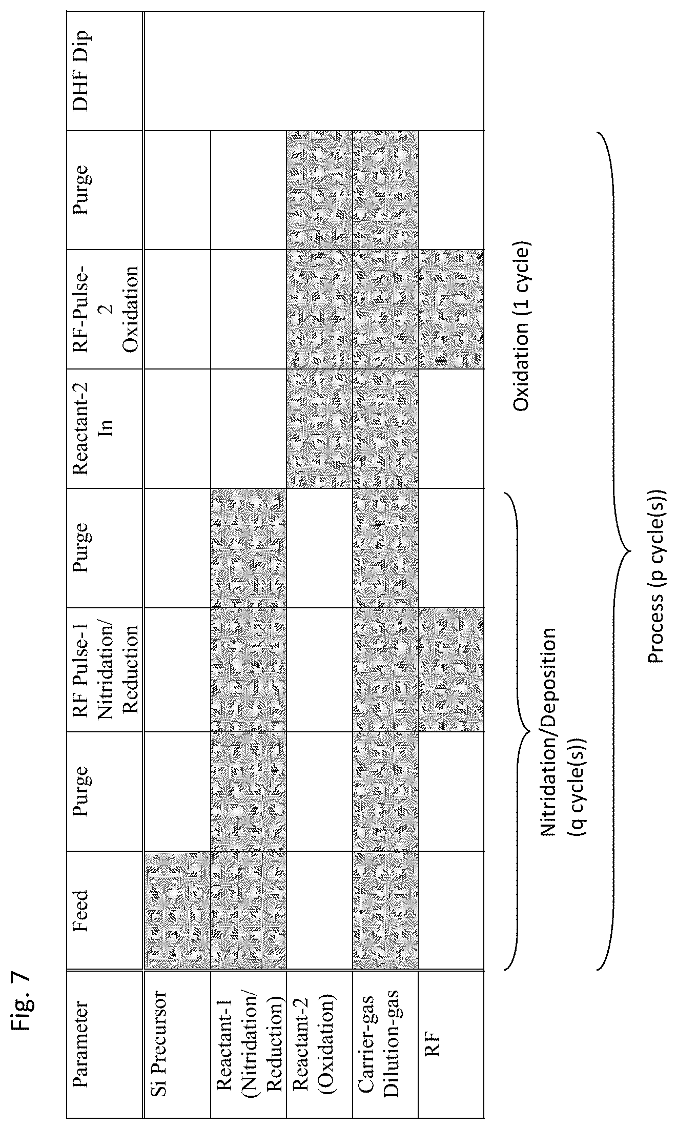
[0037] FIG. 7 is a chart illustrating the sequence of processes of topology-selective film formation according to another embodiment of the present invention, wherein a cell in gray represents an ON state whereas a cell in white represents an OFF state, and the width of each column does not represent duration of each process.
[0038] FIG. 8 is a chart showing the sequence of conventional processes of film formation, wherein a cell in gray represents an ON state whereas a cell in white represents an OFF state, and the width of each column does not represent duration of each process.
[0039] FIG. 9 illustrates schematic cross-sectional views showing the processes of topology-selective film formation according to an embodiment of the present invention.
[0040] FIG. 10 illustrates schematic cross-sectional views showing the processes of topology-selective film formation according to another embodiment of the present invention.
[0041] FIG. 11 illustrates schematic cross-sectional views showing the processes of topology-selective film formation according to still another embodiment of the present invention.
DETAILED DESCRIPTION OF EMBODIMENTS
[0042] In this disclosure, "gas" may include vaporized solid and/or liquid and may be constituted by a single gas or a mixture of gases. In this disclosure, a process gas introduced to a reaction chamber through a showerhead may be comprised of, consist essentially of, or consist of a precursor gas and an additive gas. The precursor gas and the additive gas are typically introduced as a mixed gas or separately to a reaction space. The precursor gas can be introduced with a carrier gas such as a noble gas. The additive gas may be comprised of, consist essentially of, or consist of a reactant gas and a dilution gas such as a noble gas. The reactant gas and the dilution gas may be introduced as a mixed gas or separately to the reaction space. A precursor may be comprised of two or more precursors, and a reactant gas may be comprised of two or more reactant gases. The precursor is a gas chemisorbed on a substrate and typically containing a metalloid or metal element which constitutes a main structure of a matrix of a dielectric film, and the reactant gas for deposition is a gas reacting with the precursor chemisorbed on a substrate when the gas is excited to fix an atomic layer or monolayer on the substrate. "Chemisorption" refers to chemical saturation adsorption which may be referred to also simply as "adsorption". A gas other than the process gas, i.e., a gas introduced without passing through the showerhead, may be used for, e.g., sealing the reaction space, which includes a seal gas such as a noble gas. In some embodiments, "film" refers to a layer continuously extending in a direction perpendicular to a thickness direction substantially without pinholes to cover an entire target or concerned surface, or simply a layer covering a target or concerned surface. In some embodiments, "layer" refers to a structure having a certain thickness formed on a surface or a synonym of film or a non-film structure. A film or layer may be constituted by a discrete single film or layer having certain characteristics or multiple films or layers, and a boundary between adjacent films or layers may or may not be clear and may be established based on physical, chemical, and/or any other characteristics, formation processes or sequence, and/or functions or purposes of the adjacent films or layers.
[0043] In this disclosure, "containing a Si--O bond" may refer to being characterized by a Si--O bond or Si--O bonds, having a main skeleton substantially constituted by a Si--O bond or Si--O bonds, and/or having a substituent substantially constituted by a Si--O bond or Si--O bonds. A dielectric film containing a Si--O bond includes, but is not limited to, a SiO film, a SiOC film, and a SiON film, which have a dielectric constant of about 2 to 10, typically about 4 to 8.
[0044] Further, in this disclosure, the article "a" or "an" refers to a species or a genus including multiple species unless specified otherwise. The terms "constituted by" and "having" refer independently to "typically or broadly comprising", "comprising", "consisting essentially of", or "consisting of" in some embodiments. Also, in this disclosure, any defined meanings do not necessarily exclude ordinary and customary meanings in some embodiments.
[0045] Additionally, in this disclosure, any two numbers of a variable can constitute a workable range of the variable as the workable range can be determined based on routine work, and any ranges indicated may include or exclude the endpoints. Additionally, any values of variables indicated (regardless of whether they are indicated with "about" or not) may refer to precise values or approximate values and include equivalents, and may refer to average, median, representative, majority, etc. in some embodiments.
[0046] In the present disclosure where conditions and/or structures are not specified, the skilled artisan can readily provide such conditions and/or structures, in view of the present disclosure, as a matter of routine experimentation. In all of the disclosed embodiments, any element used in an embodiment can be replaced with any elements equivalent thereto, including those explicitly, necessarily, or inherently disclosed herein, for the intended purposes. Further, the present invention can equally be applied to apparatuses and methods.
[0047] The embodiments will be explained with respect to preferred embodiments. However, the present invention is not limited to the preferred embodiments.
[0048] An exemplary embodiment is directed to a dielectric film formation process based on PEALD technology, wherein substantially only or predominantly horizontal faces of a patterned template are surface-treated by anisotropic surface treatment using a plasma, and then a film grows selectively on the surface-treated faces. The film growth occurs predominantly in a vertical direction while suppressing film growth in a horizontal direction, thereby obtaining a film profile having a desired topology. By this technology, a film can be deposited substantially only on a top face of a substrate, among the top face of the substrate and a sidewall of a recess of the substrate. The term "substantially only" refers to, e.g., 70%, 80%, 90%, or 95% or higher of the total quantity, e.g., a ratio of an average thickness of a portion of a film deposited on a top face to an average thickness of a portion of the film deposited on a sidewall is 7/3 or higher.
[0049] The degree of film formation on a bottom face depends on the aspect ratio, for example, although the bottom face is also a horizontal face. If the aspect ratio of a trench is high, e.g., 3 or higher when the opening size is 50 nm or less, the quantity of ions entering the trench becomes low as compared with that on the top face exposed to ion bombardment. As a result, surface nitridation or incubation by the surface treatment (nitridation treatment of a SiO surface) does not progress on the bottom face as much as on the top face, and thus, the thickness of a film grown on the bottom face is smaller than that of a film grown on the top face. By adjusting the aspect ratio of a recess, e.g., using a recess having an aspect ratio of 10 or higher, it is possible to deposit a film substantially on a top face, among the top face, sidewall, and bottom face.
[0050] In some embodiments, the topology selective process comprises: A) conducting anisotropic surface treatment (incubation or surface nitridation) using a plasma in a manner treating substantially only a horizontal face of a patterned substrate; B) depositing a nitride film on the surface-treated face by PEALD using a precursor containing a halogen active group and a plasma of NH.sub.3, N.sub.2/H.sub.2, and the like (nitridation by exchange reaction between halogen and nitrogen); C) changing the gas in a reaction chamber to an oxidizing atmosphere by feeding, e.g., O.sub.2 after purging the chamber, and oxidizing the nitride film by, e.g., thermal oxidation, radical oxidation, plasma oxidation, and the like so as to convert the nitride film to an oxide film; and D) repeating steps A) to C) until a thickness of the oxide film reaches a desired value wherein the oxide film has a desired topology-selective film profile.
[0051] In some embodiments, the oxide film is constituted by SiO, SiOC, SiON, and the like. Since the anisotropic surface treatment is conducted, a film grows substantially only in a vertical direction, not in a horizontal direction. By using a recess having a high aspect ratio, a film can be formed substantially only on a top face, among the top face, sidewall, and bottom face. Further, as necessary, by subjecting the finally deposited oxide film to isotropic wet etching (e.g., using dHF), a film on the sidewall can be completely removed, thereby forming a film profile wherein only a film on the top and bottom faces can remain. Further, in some embodiments, the surface treatment and the deposition process can be continuously conducted using a same reaction chamber.
[0052] In the topology-selective treatment technology, by depositing a SiN film using a carbon-free precursor and a carbon-free nitriding reactant such as N.sub.2, N.sub.2/H.sub.2, NH.sub.3, or the like, and then, converting the SiN film to a SiO film by oxidizing the SiN film using an oxidizing gas such as O.sub.2, H.sub.2O, or the like through oxidation exchange reaction, formation of a carbon-free SiO film growing on a substrate can be achieved. By this technology, accumulation of impurities included in the process gases (including the precursor and the reactant) in an interface between the SiO film and an underlying film can be suppressed while formation of the SiO film progresses.
[0053] Some embodiments provide a method for forming a silicon oxide film on a step having a top surface, a sidewall, and a bottom surface formed on a substrate, comprising processes of: (a) designing a topology of a final silicon oxide film, which is a conformal film or a film having low conformality, formed on the step by preselecting a target portion of an initial silicon nitride film to be selectively deposited or removed or reformed with reference to a non-target portion of the initial silicon nitride film resulting in the final silicon oxide film, said selectively deposited target portion being a top/bottom portion of the initial silicon nitride film formed on the top and bottom surfaces of the step, said selectively removed or reformed target portion being a sidewall portion of the initial silicon nitride film formed on the sidewall of the step; and (b) forming the initial silicon nitride film and the final silicon oxide film on the surfaces of the step according to the topology designed in process (a), wherein the initial silicon nitride film is deposited by atomic layer deposition (ALD) using a silicon-containing precursor containing halogen, and the initial silicon nitride film is converted to the final silicon oxide film by oxidizing the initial silicon nitride film without further depositing a film wherein a Si--N bond in the initial silicon nitride film is converted to a Si--O bond. FIG. 2 is a flowchart representing the above processes of topology-selective film formation. As illustrated in FIG. 2, there are three techniques used alternatively or in any combination to achieve the desired topology of the final oxide film: selective deposition of a target portion of a film, selective removal of a target portion of a film, and selective reformation of a target portion of a film.
[0054] In this disclosure, the term "step" or "recess" refers to any patterned structure constituted by a riser (sidewall) and a tread (top face) with respect to a reference plane (bottom face) formed in a substrate, and in some embodiments, the step may a trench having a width of about 10 to about 50 nm (typically about 15 to about 30 nm) (wherein when the trench has a length substantially the same as the width, it is referred to as a hole/via, and a diameter thereof is about 10 to about 50 nm), a depth of about 30 to about 200 nm (typically about 50 to about 150 nm), and an aspect ratio of about 3 to about 20 (typically about 3 to about 10). In some embodiments, the final silicon oxide film is formed selectively on the top face (having a conformality of about zero to about 10%, about 20%, or about 30% or less) or uniformly along the step or trench of the substrate (having a conformality of about 70% to about 110%, typically about 80% or higher, more typically about 90% or higher, and 100% or less) wherein the "conformality" is determined by comparing film thickness formed at some point (typically a middle point in a cross sectional view) on a sidewall or a bottom face of a recess to film thickness formed on a flat surface (top face) just outside the recess.
[0055] In some embodiments, the precursor used in process (b) contains no carbon, and the final silicon oxide film is free of carbon.
[0056] In some embodiments, the formation of the initial silicon nitride film (which may be referred to as "nitridation" wherein the nitrogen of the reactant replaces the halogen of the absorbed precursor by exchange reaction) and the oxidization of the initial silicon nitride film are continuously conducted in process (b) in a same reaction space. In some embodiments, the reaction space is purged after the formation of the initial silicon nitride film before the oxidization of the initial silicon nitride film, and the oxidization of the initial silicon nitride film is plasma oxidization conducted in the reaction space into which an oxidizing gas is introduced, which is at least one gas selected from the group consisting of O.sub.2, O.sub.3, CO.sub.2, N.sub.2O, and H.sub.2O. In this disclosure, "continuously" refers to without breaking a vacuum, without interruption as a timeline, without changing treatment conditions, immediately thereafter, as a next step, or without a discrete physical or chemical boundary between two structures in some embodiments. The nitridation is typically required to be substantially complete because any remaining halogen in the nitride film may be considered as an impurity, like carbon, which may migrate into an interface between the nitride film and an underlying film.
[0057] In some embodiments, the initial silicon nitride film is composed of multiple monolayers and, in process (b), the oxidization of the initial silicon nitride film is conducted after each monolayer deposition cycle of ALD of the initial silicon nitride film or after every multiple monolayer deposition cycles of ALD of the initial silicon nitride film.
[0058] In some embodiments the target portion preselected in process (a) is the selectively deposited target portion, wherein process (b) comprises: (ci) depositing a silicon oxide film on the surfaces of the step on the substrate; (cii) anisotropically nitriding a surface of the silicon oxide film using a nitrogen-hydrogen-containing plasma generated by applying RF power between two electrodes between which the substrate is placed in parallel to the two electrodes, in a manner nitriding the surface of the silicon oxide film predominantly on the top and bottom surfaces of the step, rather than on the sidewall of the step, thereby introducing --NH terminals on the surface of the silicon oxide film; (ciii) depositing, on and in contact with the surface-treated silicon oxide film, at least part of the initial silicon nitride film by ALD using the precursor and a nitriding gas excited by a plasma generated by applying RF power between the two electrodes; (civ) oxidizing the at least part of the initial silicon nitride film using an excited oxidizing gas to obtain at least part of the final silicon oxide film without further depositing a film wherein a Si--N bond in the initial silicon nitride film is converted to a Si--O bond; and (cv) as necessary, repeating processes (cii) and (civ) until the final silicon oxide film having a desired thickness is obtained. FIG. 3 is a flowchart representing the above processes of topology-selective film formation.
[0059] In some embodiments, the nitrogen-hydrogen-containing plasma in process (cii) is generated using a mixture of N.sub.2 and H.sub.2, NH.sub.3, other N.sub.xH.sub.y wherein x and y are integers, or a mixture of two or more of the foregoing.
[0060] In some embodiments, the silicon oxide film in process (ci) is deposited by ALD or CVD.
[0061] In some embodiments, the target portion preselected in process (a) is the selectively removed target portion, wherein process (b) comprises: (di) depositing at least part of the initial silicon nitride film on the surfaces of the step on the substrate by ALD using the precursor and a reactant gas excited by a plasma generated by applying RF power between two electrodes between which the substrate is placed in parallel to the two electrodes, wherein RF power is applied at 0.14 W/cm.sup.2 to 1.41 W/cm.sup.2 per area of the substrate for five seconds or less in each monolayer deposition cycle of ALD, thereby giving the target portion lower chemical resistance properties than those of the non-target portion when subjected to wet-etching; (dii) oxidizing the at least part of the initial silicon nitride film using an excited oxidizing gas to obtain at least part of an intermediate silicon oxide film without further depositing a film wherein a Si--N bond in the initial silicon nitride film is converted to a Si--O bond; and (diii) as necessary, repeating processes (di) and (dii) until the intermediate silicon oxide film having a desired thickness is obtained; and then (div) wet-etching the intermediate silicon oxide film to obtain the final dielectric film, thereby removing predominantly the target portion with reference to the non-target portion. FIG. 4 is a flowchart representing the above processes of topology-selective film formation.
[0062] In some embodiments, the oxidization in process (dii) is conducted using plasma, UV light, heat, or a combination of two or more of the foregoing.
[0063] In some embodiments, RF power used in process (di) is 0.14 W/cm.sup.2 to 0.71 W/cm.sup.2 per area of the substrate, and the oxidization in process (dii) is plasma oxidization conducted after each monolayer deposition cycle of ALD of the initial silicon nitride film or after every multiple monolayer deposition cycles of ALD of the initial silicon nitride film in process (di), wherein the plasma is generated by applying RF power at 0.07 W/cm.sup.2 to 0.71 W/cm.sup.2 per area of the substrate between two electrodes between which the substrate is placed in parallel to the two electrodes.
[0064] In some embodiments, process (diii) is conducted wherein immediately before repeating process (di) each time, surfaces of the step of the substrate are exposed to a hydrogen-containing reducing gas to treat the surfaces with the hydrogen-containing reducing gas.
[0065] In some embodiments, the hydrogen-containing reducing gas is at least one gas selected from the group consisting of H.sub.2 and NH.sub.3.
[0066] In some embodiments, in process (div), the wet-etching is wet-etching using dHF.
[0067] In some embodiments, the target portion preselected in process (a) is the selectively reformed target portion, wherein process (b) comprises: (ei) depositing at least part of the initial silicon nitride film on the surfaces of the step on the substrate by ALD using the precursor and a reactant gas excited by a plasma generated by applying RF power between two electrodes between which the substrate is placed in parallel to the two electrodes, wherein RF power is applied at 0.14 W/cm.sup.2 to 1.41 W/cm.sup.2 per area of the substrate for more than five seconds in each monolayer deposition cycle of ALD, thereby giving the target portion chemical resistance properties substantially equal to those of the non-target portion when subjected to wet-etching; (eii) oxidizing the at least part of the initial silicon nitride film using an excited oxidizing gas to obtain at least part of an intermediate silicon oxide film without further depositing a film wherein a Si--N bond in the initial silicon nitride film is converted to a Si--O bond; and (eiii) as necessary repeating processes (ei) and (eii) until the intermediate silicon oxide film having a desired thickness is obtained; and then (eiv) wet-etching the intermediate silicon oxide film to obtain the final dielectric film, thereby forming the final silicon oxide film having high conformality. FIG. 5 is a flowchart representing the above processes of topology-selective film formation.
[0068] In some embodiments, the oxidization in process (eii) is conducted using plasma, UV light, heat, or a combination of two or more of the foregoing.
[0069] In some embodiments, RF power used in process (ei) is 0.71 W/cm.sup.2 to 1.41 W/cm.sup.2 per area of the substrate, and the oxidization in process (eii) is plasma oxidization conducted after each monolayer deposition cycle of ALD of the initial silicon nitride film or after every multiple monolayer deposition cycles of ALD of the initial silicon nitride film in process (ei), wherein the plasma is generated by applying RF power at 0.07 W/cm.sup.2 to 0.71 W/cm.sup.2 per area of the substrate between two electrodes between which the substrate is placed in parallel to the two electrodes.
[0070] In some embodiments, process (eiii) is conducted wherein immediately before repeating process (ei) each time, surfaces of the step of the substrate are exposed to a hydrogen-containing reducing gas to treat the surfaces with the hydrogen-containing reducing gas.
[0071] In some embodiments, the hydrogen-containing reducing gas is at least one gas selected from the group consisting of H.sub.2 and NH.sub.3.
[0072] In some embodiments, in process (eiv), the wet-etching is wet-etching using dHF.
[0073] In some embodiments, the etching is wet etching using dHF, the concentration of which is approximately 0.1%.
[0074] The present invention will be explained in detail with reference to preferred embodiments illustrated in the drawings. However, the present invention is not intended to be limited to these embodiments.
[0075] FIG. 6 is a timing chart illustrating the sequence of processes of topology-selective film formation according to an embodiment of the present invention, wherein the width of each column does not necessarily represent the actual time length, and a raised level of the line in each row represents an ON-state whereas a bottom level of the line in each row represents an OFF-state. By this technique, a top-thick TS-SiO film can be formed by selective deposition of a target portion (top portion) of a film.
[0076] In FIG. 6, the selective deposition of a target portion (top portion) of a film comprises three processes: an incubation process, nitridation (deposition) process, and oxidation process. Prior to the incubation process, a silicon oxide film is deposited as an underlying film on surfaces of a step on a patterned substrate. The incubation process comprises anisotropically nitriding a surface of the silicon oxide film using a nitrogen-hydrogen-containing plasma generated using a nitriding gas (Reactant 1) by applying RF power (Treatment 3) between two electrodes between which the substrate is placed in parallel to the two electrodes, in a manner nitriding the surface of the silicon oxide film predominantly on the top and bottom surfaces of the step, rather than on the sidewall of the step, thereby introducing --NH terminals on the surface of the silicon oxide film. In the incubation process, in some embodiments, the flow rate of Reactant 1 is in a range of 500 sccm to 10000 sccm (preferably 1000 sccm to 5000 sccm), and Treatment 3 is in a range of 1 seconds to 20 seconds (preferably 3 seconds to 10 seconds).
[0077] Next, the nitridation (deposition) process begins, which comprises depositing, on and in contact with the surface-treated silicon oxide film, at least part of the initial silicon nitride film by PEALD using the precursor (Precursor) and a nitriding gas (Reactant 1) excited by a plasma generated by applying RF power (Treatment 1) between the two electrodes. Treatment 3 in the incubation process and Treatment 1 in the nitridation process are both treatment by applying RF power. Although the conditions of RF power application can be the same both in Treatment 3 and Treatment 1. However, preferably, Treatment 3 uses stronger ion energy in order to perform anisotropic surface nitridation than Treatment 1 in some embodiments. Thus, in some embodiments, in Treatment 3, higher RF power and/or lower pressure than those in Treatment 1 are used. For example, in Treatment 3, RF power in a range of 0.07 W/cm.sup.2 to 1.4 W/cm.sup.2 (preferably 0.14 W/cm.sup.2 to 0.7 W/cm.sup.2) is applied under a pressure of 100 Pa to 3000 Pa (preferably 200 Pa to 1000 Pa), whereas in Treatment 1, RF power in a range of 0.07 W/cm.sup.2 to 1.4 W/cm.sup.2 (preferably 0.14 W/cm.sup.2 to 0.7 W/cm.sup.2) is applied under a pressure of 100 Pa to 2000 Pa (preferably 200 Pa to 1000 Pa). The nitridation (deposition) process is a PEALD process, one cycle of which for forming a monolayer may be repeated at N times until a desired thickness of the nitride film is obtained, wherein N is an integer of 10 to 1000 (preferably 10 to 30), depending on the intended use of the film, etc., so as to deposit the nitride film having a thickness of 5 nm to 100 nm (preferably 10 nm to 30 nm). In one cycle of the PEALD, the duration of a pulse of Precursor, that of Reactant 1, and that of Treatment 1 are in ranges of 0.1 seconds to 20 seconds.
[0078] Thereafter, the oxidation process beings which comprises oxidizing the at least part of the initial silicon nitride film using an oxidizing gas (Reactant 2) excited by RF power (Treatment 2) to obtain at least part of the final silicon oxide film without further depositing a film wherein a Si--N bond in the initial silicon nitride film is converted to a Si--O bond. For example, in Treatment 2, RF power in a range of 0.07 W/cm.sup.2 to 1.4 W/cm.sup.2 (preferably 0.07 W/cm.sup.2 to 0.7 W/cm.sup.2) is applied under a pressure of 100 Pa to 3000 Pa (preferably 200 Pa to 1000 Pa). In the oxidation process, in some embodiments, the flow rate of Reactant 2 is in a range of 10 sccm to 1000 sccm (preferably 50 sccm to 500 sccm), and the duration of Treatment 2 is in a range of 0.1 seconds to 20 seconds (preferably 0.5 seconds to 10 seconds).
[0079] Throughout the entire processes, an inert gas (Inert gas) is fed continuously to the reaction chamber in a range of 500 sccm to 10000 sccm (preferably 1000 sccm to 5000 sccm). Also, the temperature of the processes may be in a range of 0.degree. C. to 600.degree. C. (preferably 200.degree. C. to 500.degree. C.).
[0080] Further, as necessary, the incubation process, nitridation process, and oxidation process may be repeated at M times until the final silicon oxide film having a desired thickness is obtained, wherein M is an integer of 1 to 30 (preferably 1 to 15), depending on the intended use of the film, etc.
[0081] FIG. 9 illustrates schematic cross-sectional views showing the processes of topology-selective film formation according to an embodiment represented by the timing chart illustrated in FIG. 6. State (a) represents a state prior to state (b) where a SiO film 43 is formed on a surface of a substrate 41 having steps 42 (a trench). State (b) represents a state upon the incubation process, wherein a surface of the SiO film 43 is nitrided by an anisotropic nitrogen-containing plasma so that --NH terminals are introduced on the SiO surface, thereby forming a SiNH surface 44 on the SiO film 43. State (c) represents a state upon the nitridation process, wherein a SiN film 46 is deposited and grows on the SiNH surface 44 by PEALD. When the SiN film 46 is subjected to the oxidation process, the SiN film 46 is converted to a SiN film similar to the SiN film 43 in state (a). Then, these processes are repeated, thereby obtaining a desired final SiO film (a top-thick TS-SiO film) on the substrate.
[0082] In some embodiments, the selective deposition scheme can be conducted under the conditions shown in Table 1 below.
TABLE-US-00001 TABLE 1 (numbers are approximate) Parameter Nitridation/deposition Oxidization Nitriding gas N.sub.2, N.sub.2/H.sub.2, -- NH.sub.3, NxHyCz (x, y, z .noteq. 0) Oxidizing gas -- O.sub.2, CO.sub.2, N.sub.2O, H.sub.2O Flow rate of Nitriding gas <2000 sccm -- Flow rate of Oxidizing gas -- 100-3000 sccm Number of nitridation cycle 1 to 5 per oxidization cycle
[0083] FIG. 7 is a chart illustrating the sequence of processes of topology-selective film formation according to another embodiment of the present invention, wherein a cell in gray represents an ON state whereas a cell in white represents an OFF state, and the width of each column does not represent duration of each process. By this technique, a top-thick TS-SiO film can be formed by selective removal of a target portion (sidewall) of a film, and also, a conformal TS-SiO film can be formed by selective reformation of a target portion (top face relative to sidewall) of a film.
[0084] This process sequence comprises a nitridation/deposition process ("Feed".fwdarw."Purge".fwdarw."RF Pulse-1 (Nitridation/Reduction)".fwdarw."Purge"), an oxidation process ("Reactant-2 In" "RF Pulse-2 (Oxidation)".fwdarw."Purge"), and a wet etching process ("DHF Dip"). The nitridation process comprises depositing at least part of an initial silicon nitride film on a surface of a step on a substrate by PEALD using a precursor (Si Precursor) and a reactant gas (Reactant-1) excited by a plasma generated by applying RF power (RF) between two electrodes between which the substrate is placed in parallel to the two electrodes, wherein RF power is applied at 0.14 W/cm.sup.2 to 1.41 W/cm.sup.2 per area of the substrate (preferably 0.07 W/cm.sup.2 to 0.71 W/cm.sup.2) for five seconds or less (preferably 1 second to 3 seconds) in each monolayer deposition cycle of PEALD, thereby giving the target portion (sidewall) lower chemical resistance properties (resistance to wet etching) than those of the non-target portion when subjected to wet-etching. By using the above RF power application conditions, a portion of the film deposited on the sidewall is nitrided insufficiently to sustain resistance to wet etching, as compared with a portion of the film deposited on the top/bottom face, thereby allowing for selective removal of the sidewall portion by wet etching.
[0085] The nitridation (deposition) process is a PEALD process, one cycle of which for forming a monolayer may be repeated at q times until a desired thickness of the nitride film is obtained, wherein q is an integer of 10 to 1000 (preferably 30 to 500), depending on the intended use of the film, etc., so as to deposit the nitride film having a thickness of 5 nm to 100 nm (preferably 10 nm to 30 nm). In one cycle of the PEALD, the duration of a pulse of "Si-Precursor," that of "Reactant-1," and that of "RF" are in ranges of 0.1 seconds to 20 seconds (preferably 0.1 seconds to 10 seconds). In some embodiments, RF power is applied under a pressure of 100 Pa to 2000 Pa (preferably 200 Pa to 1000 Pa). In the nitridation process, in some embodiments, the flow rate of Reactant-1 is in a range of 500 sccm to 10000 sccm (preferably 2000 sccm to 5000 sccm). In this embodiment, "Reactant-1" and "Carrier gas/Dilution gas" flow continuously.
[0086] Next, the oxidation process begins, which comprises oxidizing the at least part of the initial silicon nitride film using an oxidizing gas (Reactant-2) excited by RF power (RF) to obtain at least part of an intermediate silicon oxide film without further depositing a film wherein a Si--N bond in the initial silicon nitride film is converted to a Si--O bond. For example, RF power in a range of 0.07 W/cm.sup.2 to 1.4 W/cm.sup.2 (preferably 0.07 W/cm.sup.2 to 0.7 W/cm.sup.2) is applied under a pressure of 100 Pa to 2000 Pa (preferably 200 Pa to 1000 Pa). In the oxidation process, in some embodiments, the flow rate of "Reactant-2" is in a range of 10 sccm to 1000 sccm (preferably 50 sccm to 500 sccm), and the duration of "RF" is in a range of 0.1 seconds to 10 seconds (preferably 0.1 seconds to 5 seconds).
[0087] Throughout the entire process, a carrier gas and/or dilution gas can be fed continuously to the reaction chamber in a range of 500 sccm to 10000 sccm (preferably 1000 sccm to 5000 sccm). Also, the temperature of the processes may be in a range of 0.degree. C. to 600.degree. C. (preferably 200.degree. C. to 500.degree. C.).
[0088] Further, as necessary, the nitridation/deposition process and the oxidation process are repeated at p times until the intermediate silicon oxide film having a desired thickness is obtained, wherein p is an integer of 1 to 30 (preferably 1 to 15), depending on the intended use of the film, etc.
[0089] Thereafter, the wet etching process (DHF Dip) begins, which comprises wet-etching the intermediate silicon oxide film to obtain the final dielectric film, thereby removing predominantly the target portion (sidewall) with reference to the non-target portion. In some embodiments, wet etching can be performed by etching the substrate using a hydrofluoric acid or its known or new suitable equivalent/substitute diluted at 0.1% to 1.5% at a temperature of 15.degree. C. to 25.degree. C. for 30 seconds to 600 seconds.
[0090] FIG. 10 illustrates schematic cross-sectional views showing the processes of topology-selective film formation according to an embodiment represented by the process sequence illustrated in FIG. 7. State (a) represents a state upon the nitridation/deposition process, wherein a SiN film 53 is formed on a surface of a substrate 51 having steps 52 (a trench). State (b) represents a state upon the oxidation process, wherein the SiN film 53 is subjected to the oxidation process, and the SiN film 53 is converted to a SiO film 54. Thereafter, as necessary, the nitridation/deposition process and the oxidation process are repeated until a desired thickness of the SiO film is obtained. State (c) represents a state upon wet etching, wherein by wet etching, since the portion of the film deposited on the sidewall has lower resistance to wet etching than that of the portion of the top/bottom faces, the sidewall portion of the film can selectively significantly be removed or selectively completely be removed while the other portions can maintain a significant thickness. Accordingly, a desired final SiO film (a top-thick TS-SiO film) can be formed on the substrate.
[0091] By using the same processes illustrated in FIG. 7 except that RF power applied between the two electrodes is 0.14 W/cm.sup.2 to 1.41 W/cm.sup.2 per area of the substrate (preferably 0.07 W/cm.sup.2 to 0.71 W/cm.sup.2) for more than five seconds in each monolayer deposition cycle of ALD, the film properties of a resultant SiO film such as resistance to wet etching can become substantially equal among a portion of the film deposited on the top face, a portion of the film deposited on the sidewall, and a portion of the film deposited on the bottom face, whereby, after wet etching, a conformal SiO film (carbon-free) can be formed.
[0092] FIG. 11 illustrates schematic cross-sectional views showing the processes of topology-selective film formation represented by the process sequence illustrated in FIG. 7 which is modified as discussed above. State (a) represents a state upon the nitridation/deposition process, wherein a SiN film 63 is formed on a surface of a substrate 61 having steps 62 (a trench). State (b) represents a state upon the oxidation process, wherein the SiN film 63 is subjected to the oxidation process, and the SiN film 63 is converted to a SiO film 64. Thereafter, as necessary, the nitridation/deposition process and the oxidation process are repeated until a desired thickness of the SiO film is obtained. State (c) represents a state upon wet etching, wherein by wet etching, since the portion of the film deposited on the top face, the portion of the film deposited on the sidewall, and the portion of the film deposited on the bottom face have substantially similar resistance to wet etching, all the portions are substantially equally etched as necessary. Accordingly, a desired final SiO film (a conformal carbon-free, homogenous TS-SiO film) can be formed on the substrate.
[0093] In some embodiments, the nitridation in the selective removal of a target portion (FIG. 10) and the selective reformation of a target portion (FIG. 11) can be conducted under the conditions shown in Table 2 below.
TABLE-US-00002 TABLE 2 (numbers are approximate) Parameter Selective reform Selective removal Reactant gas N.sub.2, N.sub.2/H.sub.2, N.sub.2, N.sub.2/H.sub.2, NH.sub.3, NxHyCz NH.sub.3, NxHyCz (x, y, z .noteq. 0) (x, y, z .noteq. 0) Reactant flow (F) F1 = 2000-5000 sccm F2 = <2000 sccm (F1 < F2) RF power @ RFP1 = 200-500 W RFP2 = 200-1000 W 300 mm-wafer (RFP1 < RFP2) (PFP) Duration of RF (DRF) DRF1 = More DRF2 = No more than 3 sec. than 5 sec. (preferably more (preferably no more than 5 sec.) than 3 sec.) (DRF1 > DRF2)
[0094] In some embodiments, in the selective reform scheme, in order to improve conformality of the film, the flow rate of a nitrogen-containing gas is greater than that in the selective removal scheme, and also, the RF power application time is longer than that in the selective removal scheme. In other words, in some embodiments, in the selective removal scheme, in order to increase growth of a film on a flat (horizontal) surface relative to that on a vertical surface, the flow rate of a nitrogen-containing gas is less than that in the selective reform scheme, and also, the RF power application time is shorter than that in the selective reform scheme.
[0095] FIG. 8 is a chart showing the sequence of conventional processes of film formation, wherein a cell in gray represents an ON state whereas a cell in white represents an OFF state, and the width of each column does not represent duration of each process. Since in the conventional processes, no processes corresponding or equivalent to those discussed above in relation to the embodiments of the present invention are conducted, logically, a conformal carbon-free, homogenous SiO film will not be formed.
[0096] In the process sequence described in this disclosure, the precursor may be supplied in a pulse using a carrier gas which is continuously supplied. This can be accomplished using a flow-pass system (FPS) wherein a carrier gas line is provided with a detour line having a precursor reservoir (bottle), and the main line and the detour line are switched, wherein when only a carrier gas is intended to be fed to a reaction chamber, the detour line is closed, whereas when both the carrier gas and a precursor gas are intended to be fed to the reaction chamber, the main line is closed and the carrier gas flows through the detour line and flows out from the bottle together with the precursor gas. In this way, the carrier gas can continuously flow into the reaction chamber and can carry the precursor gas in pulses by switching the main line and the detour line. FIG. 1B illustrates a precursor supply system using a flow-pass system (FPS) according to an embodiment of the present invention (black valves indicate that the valves are closed). As shown in (a) in FIG. 1B, when feeding a precursor to a reaction chamber (not shown), first, a carrier gas such as Ar (or He) flows through a gas line with valves b and c, and then enters a bottle (reservoir) 30. The carrier gas flows out from the bottle 30 while carrying a precursor gas in an amount corresponding to a vapor pressure inside the bottle 30, and flows through a gas line with valves f and e, and is then fed to the reaction chamber together with the precursor. In the above, valves a and d are closed. When feeding only the carrier gas (noble gas) to the reaction chamber, as shown in (b) in FIG. 1B, the carrier gas flows through the gas line with the valve a while bypassing the bottle 30. In the above, valves b, c, d, e, and f are closed.
[0097] The precursor may be provided with the aid of a carrier gas. Since ALD is a self-limiting adsorption reaction process, the number of deposited precursor molecules is determined by the number of reactive surface sites and is independent of precursor exposure after saturation, and a supply of the precursor is such that the reactive surface sites are saturated thereby per cycle. A plasma for deposition may be generated in situ, for example, in an ammonia gas that flows continuously throughout the deposition cycle. In other embodiments the plasma may be generated remotely and provided to the reaction chamber.
[0098] As mentioned above, each pulse or phase of each deposition cycle is preferably self-limiting. An excess of reactants is supplied in each phase to saturate the susceptible structure surfaces. Surface saturation ensures reactant occupation of all available reactive sites (subject, for example, to physical size or "steric hindrance" restraints) and thus ensures excellent step coverage. In some embodiments the pulse time of one or more of the reactants can be reduced such that complete saturation is not achieved and less than a monolayer is adsorbed on the substrate surface.
[0099] The process cycle can be performed using any suitable apparatus including an apparatus illustrated in FIG. 1A, for example. FIG. 1A is a schematic view of a PEALD apparatus, desirably in conjunction with controls programmed to conduct the sequences described below, usable in some embodiments of the present invention. In this figure, by providing a pair of electrically conductive flat-plate electrodes 4, 2 in parallel and facing each other in the interior 11 (reaction zone) of a reaction chamber 3, applying HRF power (13.56 MHz or 27 MHz) 20 to one side, and electrically grounding the other side 12, a plasma is excited between the electrodes. A temperature regulator is provided in a lower stage 2 (the lower electrode), and a temperature of a substrate 1 placed thereon is kept constant at a given temperature. The upper electrode 4 serves as a shower plate as well, and reactant gas (and noble gas) and precursor gas are introduced into the reaction chamber 3 through a gas line 21 and a gas line 22, respectively, and through the shower plate 4. Additionally, in the reaction chamber 3, a circular duct 13 with an exhaust line 7 is provided, through which gas in the interior 11 of the reaction chamber 3 is exhausted. Additionally, a dilution gas is introduced into the reaction chamber 3 through a gas line 23. Further, a transfer chamber 5 disposed below the reaction chamber 3 is provided with a seal gas line 24 to introduce seal gas into the interior 11 of the reaction chamber 3 via the interior 16 (transfer zone) of the transfer chamber 5 wherein a separation plate 14 for separating the reaction zone and the transfer zone is provided (a gate valve through which a wafer is transferred into or from the transfer chamber 5 is omitted from this figure). The transfer chamber is also provided with an exhaust line 6. In some embodiments, the deposition of multi-element film and surface treatment are performed in the same reaction space, so that all the steps can continuously be conducted without exposing the substrate to air or other oxygen-containing atmosphere. In some embodiments, a remote plasma unit can be used for exciting a gas.
[0100] In some embodiments, in the apparatus depicted in FIG. 1A, the system of switching flow of an inactive gas and flow of a precursor gas illustrated in FIG. 1B (described earlier) can be used to introduce the precursor gas in pulses without substantially fluctuating pressure of the reaction chamber.
[0101] In some embodiments, a dual chamber reactor (two sections or compartments for processing wafers disposed close to each other) can be used, wherein a reactant gas and a noble gas can be supplied through a shared line whereas a precursor gas is supplied through unshared lines.
[0102] A skilled artisan will appreciate that the apparatus includes one or more controller(s) (not shown) programmed or otherwise configured to cause the deposition and reactor cleaning processes described elsewhere herein to be conducted. The controller(s) are communicated with the various power sources, heating systems, pumps, robotics, and gas flow controllers or valves of the reactor, as will be appreciated by the skilled artisan.
[0103] The present invention is further explained with reference to working examples below. However, the examples are not intended to limit the present invention. In the examples where conditions and/or structures are not specified, the skilled artisan in the art can readily provide such conditions and/or structures, in view of the present disclosure, as a matter of routine experimentation. Also, the numbers applied in the specific examples can be modified by a range of at least .+-.50% in some embodiments, and the numbers are approximate.
EXAMPLES
Example 1
[0104] In this example, the selective reformation of a target portion of a film as illustrated in FIG. 5 was conducted. First, a SiN film having a thickness of 20 nm was formed on a Si substrate (0300 mm) having trenches (having an opening of 30 nm and an aspect ratio of 3) by PEALD, and then, the SiN film was converted to a SiO film according to the process sequence illustrated in FIG. 7 under the common conditions shown in Table 3 and the specific conditions shown in Table 4 below using the PEALD apparatus illustrated in FIG. 1A and a gas supply system (FPS) illustrated in FIG. 1B. Thereafter, the substrate was subjected to wet etching under the conditions shown in Table 3 below. As comparative examples, a SiO film was deposited in a manner similar to the above according to the process sequence illustrated in FIG. 8 wherein no nitridation/deposition process and no oxidation (conversion) process were conducted.
TABLE-US-00003 TABLE 3 (numbers are approximate) Common Conditions for Nitridation/Deposition Substrate temperature 300.degree. C. Pressure 400 Pa Dilution gas Ar (1 slm) RF power (13.56 MHz) for a 300-mm wafer 200 W Duration of RF power application per cycle 3 sec Distance between electrodes 12 mm Common Conditions for Oxidation Substrate temperature 300.degree. C. Pressure 400 Pa RF power (13.56 MHz) for a 300-mm wafer 100 W Duration of RF power application 1 sec Conditions for Wet etching Etching solution 1% HF Etching solution temperature and duration 25.degree. C., 1 min.
TABLE-US-00004 TABLE 4 (numbers are approximate) Nitridation Oxidization Number of Carrier Reactant 1 Reactant 2 nitridation Sample Precursor-1 (slm) (slm) (slm) cycle (q) Sequence Comp. 1 Bisdiethyl- Ar (2) O2 (0.5) -- FIG. 8 Aminosilane Comp. 2 Bisdiethyl- Ar (2) O2 (0.5) -- FIG. 8 Aminosilane Comp. 3 Tetrakis-ethyl-silane Ar (2) O2 (0.5) -- FIG. 8 Ex. 1 Hexa-chloro-disilane Ar (2) NH3 (2) O2 (0.5) 10 FIG. 7 Ex. 2 Hexa-chloro-disilane Ar (2) H2/N2 (2/2) O2 (0.5) 10 FIG. 7 Ex. 3 Di-iodine-silane N2 (2) NH3 (2) O2 (0.5) 10 FIG. 7 Ex. 4 Di-iodine-silane N2 (2) H2/N2-2/2 O2 (0.5) 10 FIG. 7 Ex. 5 Di-chloro-silane Ar (2) NH3 (2) O2 (0.5) 10 FIG. 7 Ex. 6 Di-chloro-silane Ar (2) H2/N2 (2/2) O2 (0.5) 10 FIG. 7 Ex. 7 Hexa-chloro-disilane Ar (2) NH3 (2) O2 (0.5) 10 FIG. 7
[0105] Each SiO film was evaluated, and the results are shown in Table 5 below.
TABLE-US-00005 TABLE 5 (numbers are approximate) GPC Trend by Side 100:1 purge Film GPC Coverage PLE DHF-WERR Carbon Nitrogen Sample Time Composition (nm/cycle) (%) (%) (TOX Ratio) (at %) (at %) Comp.1 Saturated SiO(C) 0.06 90 90 3.0 <5 ND Comp.2 Saturated SiO(C) 0.04 80 90 2.0 <5 ND Comp.3 Saturated SiO(C) 0.02 80 90 2.5 <5 ND Ex. 1 Saturated SiO 0.0 90 90 2.1 ND ND Ex. 2 Saturated SiO 0.03 95 90 2.0 ND ND Ex. 3 Saturated SiO 0.02 80 85 1.8 ND ND Ex. 4 Saturated SiO 0.04 94 88 2.1 ND ND Ex. 5 Saturated SiO 0.05 93 90 2.2 ND ND Ex. 6 Saturated SiO 0.05 93 90 1.9 ND ND Ex. 7 Saturated SiO 0.08 93 100 1.9 ND ND
[0106] In Table 5, "Saturated" in "GPC Trend by purge Time" indicates that according to GPC (growth per cycle), the purging process was conducted in a manner that a reaction process in each cycle of PEALD was performed at saturation of adsorbed precursor; "Side Coverage" refers to conformality (%); "PLE" refers to a ratio of narrow dimension and wide dimension; "100:1 DHF-WERR (TOX Ratio)" refers to wet etch rate relative to that of thermal oxide film using a hydrofluoric acid diluted at 1%; "<5" in "Carbon" refers to carbon detected at less than 5 at %; and "ND" refers to "not detected."
[0107] As shown in Table 5, according to the examples, the SiO films obtained in all the examples were high-quality conformal carbon-free SiO films, whereas in the comparative examples, the SiO films were lower quality SiOC films.
[0108] It will be understood by those of skill in the art that numerous and various modifications can be made without departing from the spirit of the present invention. Therefore, it should be clearly understood that the forms of the present invention are illustrative only and are not intended to limit the scope of the present invention.
* * * * *
D00000
D00001
D00002
D00003
D00004
D00005
D00006
D00007
D00008
D00009
XML
uspto.report is an independent third-party trademark research tool that is not affiliated, endorsed, or sponsored by the United States Patent and Trademark Office (USPTO) or any other governmental organization. The information provided by uspto.report is based on publicly available data at the time of writing and is intended for informational purposes only.
While we strive to provide accurate and up-to-date information, we do not guarantee the accuracy, completeness, reliability, or suitability of the information displayed on this site. The use of this site is at your own risk. Any reliance you place on such information is therefore strictly at your own risk.
All official trademark data, including owner information, should be verified by visiting the official USPTO website at www.uspto.gov. This site is not intended to replace professional legal advice and should not be used as a substitute for consulting with a legal professional who is knowledgeable about trademark law.