Parameter-stable Misregistration Measurement Amelioration In Semiconductor Devices
LEVINSKI; Vladimir ; et al.
U.S. patent application number 16/496918 was filed with the patent office on 2021-01-21 for parameter-stable misregistration measurement amelioration in semiconductor devices. The applicant listed for this patent is KLA CORPORATION. Invention is credited to Sharon AHARON, Vladimir LEVINSKI, Amnon MANASSEN, Yuri PASKOVER.
| Application Number | 20210020480 16/496918 |
| Document ID | / |
| Family ID | 1000005167964 |
| Filed Date | 2021-01-21 |

| United States Patent Application | 20210020480 |
| Kind Code | A1 |
| LEVINSKI; Vladimir ; et al. | January 21, 2021 |
PARAMETER-STABLE MISREGISTRATION MEASUREMENT AMELIORATION IN SEMICONDUCTOR DEVICES
Abstract
A parameter-stable misregistration measurement amelioration system and method including providing a wafer, including a plurality of multi-layered semiconductor devices formed thereon, selected from a batch wafers intended to be identical, using a misregistration metrology tool to measure misregistration at multiple sites between at least a first layer and a second layer of the wafer, using a plurality of sets of measurement parameters, thereby generating measured misregistration data for each of the sets of measurement parameters, identifying and removing a parameter-dependent portion and a mean error portion from the measured misregistration data for the wafer for each of the sets of measurement parameters, thereby generating ameliorated parameter-stable ameliorated misregistration data for the wafer.
| Inventors: | LEVINSKI; Vladimir; (Migdal Ha'emek, IL) ; PASKOVER; Yuri; (Binyamina, IL) ; AHARON; Sharon; (Hanaton, IL) ; MANASSEN; Amnon; (Haifa, IL) | ||||||||||
| Applicant: |
|
||||||||||
|---|---|---|---|---|---|---|---|---|---|---|---|
| Family ID: | 1000005167964 | ||||||||||
| Appl. No.: | 16/496918 | ||||||||||
| Filed: | August 23, 2019 | ||||||||||
| PCT Filed: | August 23, 2019 | ||||||||||
| PCT NO: | PCT/US2019/047797 | ||||||||||
| 371 Date: | September 23, 2019 |
Related U.S. Patent Documents
| Application Number | Filing Date | Patent Number | ||
|---|---|---|---|---|
| 62821596 | Mar 21, 2019 | |||
| Current U.S. Class: | 1/1 |
| Current CPC Class: | G01N 21/21 20130101; G01N 21/9501 20130101; H01L 23/544 20130101; H01L 22/12 20130101; H01L 21/67259 20130101; G01N 21/47 20130101; G03F 7/70633 20130101; H01L 2924/00 20130101 |
| International Class: | H01L 21/67 20060101 H01L021/67; G01N 21/47 20060101 G01N021/47; G01N 21/21 20060101 G01N021/21; G01N 21/95 20060101 G01N021/95 |
Claims
1. A parameter-stable misregistration measurement amelioration method comprising: providing a wafer, comprising a plurality of multilayered semiconductor devices formed thereon, selected from a batch wafers intended to be identical; using a misregistration metrology tool to measure misregistration at multiple sites between at least a first layer and a second layer of said wafer, using a plurality of sets of measurement parameters, thereby generating measured misregistration data for each of said sets of measurement parameters; identifying and removing a parameter-dependent portion and a mean error portion from said measured misregistration data for said wafer for each of said sets of measurement parameters, thereby generating ameliorated parameter-stable ameliorated misregistration data for said wafer.
2. The parameter-stable misregistration measurement amelioration method of claim 1, wherein said sets of measurement parameters comprise at least multiple wavelengths of light used in misregistration measurement.
3. The parameter-stable misregistration measurement amelioration method of claim 1, wherein said identifying said parameter-dependent portion and said mean error portion comprises: identifying a parameter-dependent portion for said measured misregistration data for each of said sets of measurement parameters; identifying at least one principal component of said parameter-dependent portion of said misregistration data for each of said sets of measurement parameters; identifying a weighting coefficient for said at least one principal component of said parameter-dependent portion of said measured misregistration data for each of said sets of parameters; and identifying at least one mean error portion, each of said mean error portions corresponding to each of said at least one principal components of said parameter-dependent portion of said measured misregistration data for each of said sets of measurement parameters.
4. The parameter-stable misregistration measurement amelioration method of claim 1, further comprising using said parameter-dependent portion and said mean error portion to identify and remove a parameter-dependent portion and a mean error portion from measured misregistration data for at least one additional wafer selected from said batch wafers intended to be identical, for each of said sets of measurement parameters, thereby generating ameliorated parameter-stable ameliorated misregistration data for said at least one additional wafer.
5. The parameter-stable misregistration measurement amelioration method of claim 1, wherein said misregistration metrology tool is an imaging misregistration metrology tool or a scatterometry misregistration metrology tool.
6. (canceled)
7. The parameter-stable misregistration measurement amelioration method of claim 1, wherein said at least one principal component of said parameter-dependent portion of said misregistration data for each of said sets of measurement parameters is identified using principal component analysis.
8. The parameter-stable misregistration measurement amelioration method of claim 1, wherein said mean error portions are identified using a reference misregistration value.
9. The parameter-stable misregistration measurement amelioration method of claim 8, wherein said reference misregistration value is generated by using a reference misregistration metrology tool to measure said wafer.
10. The parameter-stable misregistration measurement amelioration method of claim 9, wherein said reference misregistration tool is an electron beam misregistration metrology tool.
11-13. (canceled)
14. The parameter-stable misregistration measurement amelioration method of claim 1, wherein said sets of measurement parameters comprise at least one of: a focus variability in misregistration measurement; a numerical aperture used in misregistration measurement; an angle of incidence of light used in misregistration measurement; or a polarization of light used in misregistration measurement.
15. A parameter-stable misregistration measurement amelioration system comprising: a misregistration metrology tool operative to measure misregistration at multiple sites between at least a first layer and a second layer of a wafer, comprising a plurality of multilayered semiconductor devices formed thereon, selected from a batch of wafers intended to be identical, using a plurality of sets of measurement parameters, thereby generating measured misregistration data for each of said parameters; and a misregistration data analyzer operative to: identify and remove a parameter-dependent portion and a mean error portion from said measured misregistration data for said wafer for each of said sets of measurement parameters, thereby generating ameliorated parameter-stable ameliorated misregistration data for said wafer.
16. The parameter-stable misregistration measurement amelioration system of claim 15, wherein said sets of measurement parameters comprise at least multiple wavelengths of light used in misregistration measurement.
17. The parameter-stable misregistration measurement amelioration system of claim 15, wherein said misregistration data analyzer is further operative to: identify a parameter-dependent portion for said measured misregistration data for each of said sets of measurement parameters; identify at least one principal component of said parameter-dependent portion of said misregistration data for each of said sets of measurement parameters; identify a weighting coefficient for said at least one principal component of said parameter-dependent portion for said measured misregistration data for each of said sets of measurement parameters; and identify at least one mean error portion, each of said at least one mean error portion corresponding to each of said at least one principal components of said parameter-dependent portion of said measured misregistration data for each of said sets of measurement parameters.
18. The parameter-stable misregistration measurement amelioration system of claim 15, wherein said analyzer is further operative to use said parameter-dependent portion and said mean error portion to identify and remove said parameter-dependent portion and a mean error portion from said measured misregistration data for at least one additional wafer selected from said batch of wafers intended to be identical, for each of said sets of measurement parameters, thereby generating ameliorated parameter-stable ameliorated misregistration data for said at least one additional wafer.
19. The parameter-stable misregistration measurement amelioration system of claim 15, wherein said misregistration metrology tool is an imaging misregistration metrology tool or a scatterometry misregistration metrology tool.
20. (canceled)
21. The parameter-stable misregistration measurement amelioration system of claim 15, wherein said at least one principal component of said parameter-dependent portion of said misregistration data for each of said sets of measurement parameters is identified using principal component analysis.
22. The parameter-stable misregistration measurement amelioration system of claim 15, wherein said mean error portions are identified using a reference misregistration value.
23. The parameter-stable misregistration measurement amelioration system of claim 22, wherein said reference misregistration value is generated by using a reference misregistration metrology tool to measure said wafer.
24. The parameter-stable misregistration measurement amelioration system of claim 23, wherein said reference misregistration tool is an electron beam misregistration metrology tool.
25-27. (canceled)
28. The parameter-stable misregistration measurement amelioration system of claim 15, wherein said sets of measurement parameters comprise at least one of: a focus variability in misregistration measurement; a numerical aperture used in misregistration measurement; an angle of incidence of light used in misregistration measurement; or a polarization of light used in misregistration measurement.
Description
REFERENCE TO RELATED APPLICATIONS
[0001] Reference is hereby made to U.S. Provisional Patent Application Ser. No. 62/821,596, filed Mar. 21, 2019 and entitled DYNAMIC ACCURACY OPTIMIZATION BASED ON OVERLAY ERROR VARIATION WITH MEASUREMENT CONDITIONS, the disclosure of which is hereby incorporated by reference and priority of which is hereby claimed.
FIELD OF THE INVENTION
[0002] The present invention relates measurement of misregistration in the manufacture of semiconductor devices generally.
BACKGROUND OF THE INVENTION
[0003] Various methods and systems are known for measurement of misregistration in the manufacture of semiconductor devices.
SUMMARY OF THE INVENTION
[0004] The present invention seeks to provide an improved methods and systems for measurement of misregistration in the manufacture of semiconductor devices.
[0005] There is thus provided in accordance with a preferred embodiment of the present invention a parameter-stable misregistration measurement amelioration method including providing a wafer, including a plurality of multilayered semiconductor devices formed thereon, selected from a batch wafers intended to be identical, using a misregistration metrology tool to measure misregistration at multiple sites between at least a first layer and a second layer of the wafer, using a plurality of sets of measurement parameters, thereby generating measured misregistration data for each of the sets of measurement parameters, identifying and removing a parameter-dependent portion and a mean error portion from the measured misregistration data for the wafer for each of the sets of measurement parameters, thereby generating ameliorated parameter-stable ameliorated misregistration data for the wafer.
[0006] In accordance with a preferred embodiment of the present invention, the sets of measurement parameters comprise at least multiple wavelengths of light used in misregistration measurement.
[0007] Preferably, the identifying the parameter-dependent portion and the mean error portion includes identifying a parameter-dependent portion for the measured misregistration data for each of the sets of measurement parameters, identifying is at least one principal component of the parameter-dependent portion of the misregistration data for each of the sets of measurement parameters, identifying a weighting coefficient for the at least one principal component of the parameter-dependent portion of the measured misregistration data for each of the sets of parameters and identifying at least one mean error portion, each of the mean error portions corresponding to each of the at least one principal components of the parameter-dependent portion of the measured misregistration data for each of the sets of measurement parameters.
[0008] In accordance with a preferred embodiment of the present invention the parameter-stable misregistration measurement amelioration method also includes using the parameter-dependent portion and the mean error portion to identify and remove a parameter-dependent portion and a mean error portion from measured misregistration data for at least one additional wafer selected from the batch wafers intended to be identical, for each of the sets of measurement parameters, thereby generating ameliorated parameter-stable ameliorated misregistration data for the at least one additional wafer.
[0009] In accordance with a preferred embodiment of the present invention, the misregistration metrology tool is an imaging misregistration metrology tool. Alternatively, in accordance with a preferred embodiment of the present invention, the misregistration metrology tool is a scatterometry misregistration metrology tool.
[0010] Preferably, the at least one principal component of the parameter-dependent portion of the misregistration data for each of the sets of measurement parameters is identified using principal component analysis.
[0011] In accordance with a preferred embodiment of the present invention, the mean error portions are identified using a reference misregistration value. Preferably, the reference misregistration value is generated by using a reference misregistration metrology tool to measure the wafer. Preferably, the reference misregistration tool is an electron beam misregistration metrology tool.
[0012] Alternatively, in accordance with a preferred embodiment of the present invention, the mean error portions are identified using a statistical model. Preferably, the statistical model is compiled from multiple misregistration measurements of the wafer. Preferably, the statistical model includes a modeled portion and an unmodeled portion.
[0013] In accordance with a preferred embodiment of the present invention, the sets of measurement parameters comprise at least one of a focus variability in misregistration measurement, a numerical aperture used in misregistration measurement, an angle of incidence of light used in misregistration measurement and a polarization of light used in misregistration measurement.
[0014] There is also provided in accordance with another preferred embodiment of the present invention a parameter-stable misregistration measurement amelioration system including a misregistration metrology tool operative to measure misregistration at multiple sites between at least a first layer and a second layer of a wafer, including a plurality of multilayered semiconductor devices formed thereon, selected from a batch of wafers intended to be identical, using a plurality of sets of measurement parameters, thereby generating measured misregistration data for each of the parameters and a misregistration data analyzer operative to identify and remove a parameter-dependent portion and a mean error portion from the measured misregistration data for the wafer for each of the sets of measurement parameters, thereby generating ameliorated parameter-stable ameliorated misregistration data for the wafer.
BRIEF DESCRIPTION OF THE DRAWINGS
[0015] The present invention will be understood and appreciated more fully from the following detailed description, taken in conjunction with the drawings in which:
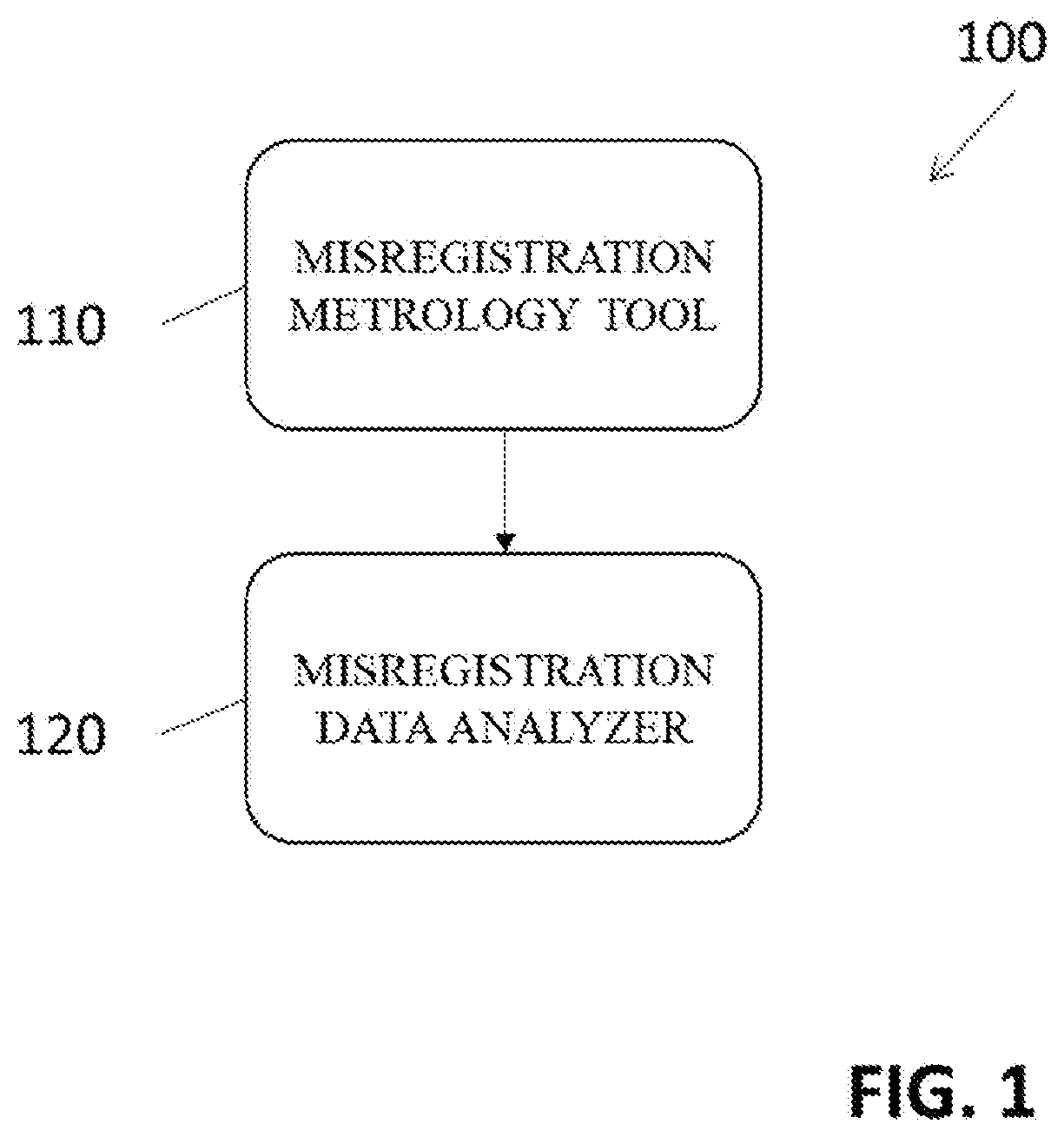
[0016] FIG. 1 is a simplified schematic illustration of a parameter-stable misregistration measurement amelioration system; and
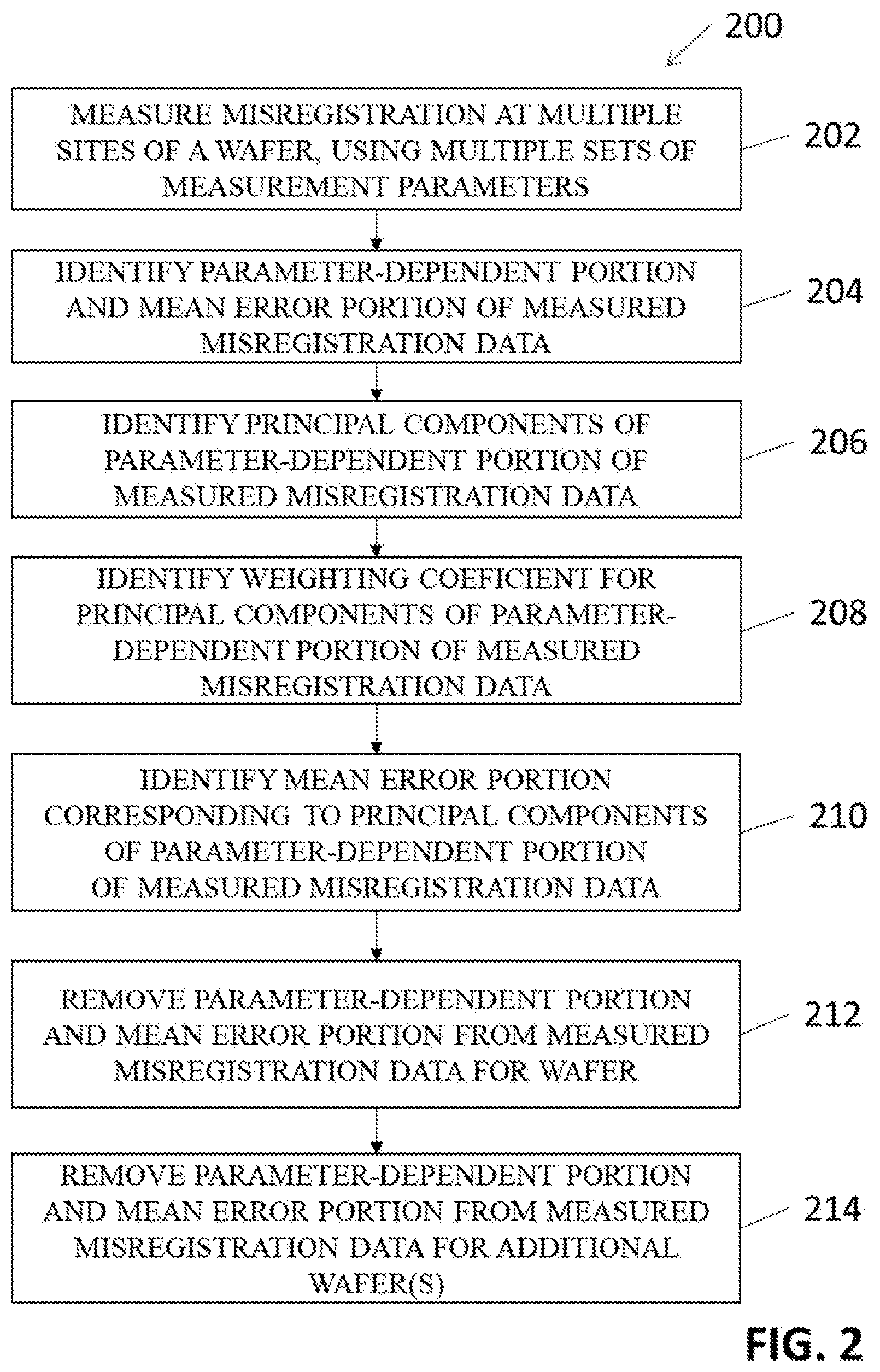
[0017] FIG. 2 is a simplified flow chart illustrating a parameter-stable misregistration measurement amelioration method useful by the parameter-stable misregistration measurement amelioration system of FIG. 1.
DETAILED DESCRIPTION OF PREFERRED EMBODIMENTS
[0018] It is appreciated that the system and method described hereinbelow with reference to FIGS. 1 & 2 form part of a manufacturing process for semiconductor devices, and the misregistration measured by the system and method described hereinbelow with reference to FIGS. 1 & 2 is used to adjust fabrication processes of the semiconductor devices to more closely align various layers of the semiconductor devices being fabricated.
[0019] Reference is now made to FIG. 1, which is a simplified schematic illustration of a parameter-stable misregistration measurement amelioration system (PSMMAS) 100, and to FIG. 2, which is a simplified flow chart illustrating a parameter-stable misregistration measurement amelioration method (PSMMAM) 200 useful by PSMMAS 100.
[0020] As seen in FIG. 1, PSMMAS 100 includes a misregistration metrology tool 110 and a misregistration data analyzer 120. Misregistration metrology tool 110 can be any suitable misregistration metrology tool, having the capability to measure misregistration using a plurality of sets of measurement parameters, such as an imaging misregistration metrology tool or a scatterometry misregistration metrology tool. Preferably, the parameters include multiple wavelengths of light used in measuring misregistration. A typical imaging misregistration metrology tool forming part of PSMMAS 100 is an Archer.TM. 700, commercially available from KLA Corporation, of Milpitas, Calif. A typical scatterometry misregistration metrology tool forming part of PSMMAS 100 is an ATL100.TM., commercially available from KLA Corporation, of Milpitas, Calif.
[0021] As seen in FIG. 2, at a first step 202, a wafer, including a plurality of multilayered semiconductor devices formed thereon, selected from a batch of wafers intended to be identical, is provided, and misregistration metrology tool 110 measures misregistration, also referred to as overlay, at multiple sites, s, between at least a first layer and a second layer of the wafer, using multiple sets of measurement parameters, .lamda., preferably including multiple wavelengths of light, thereby generating measured misregistration data, OVL(.lamda.,s), for each site and for each of the sets of parameters. It is appreciated that each of the wafers in the batch of wafers intended to be identical undergo the same fabrication steps and include semiconductor devices intended to be identical to corresponding semiconductor devices on all other wafers in the batch of wafers intended to be identical.
[0022] Typically, the wafer measured at step 202 includes features having some number, n, of deformations included in each of the measured sites. Thus, measured misregistration data, OVL(.lamda.,s), may include components from both a misregistration between the first and second layers OVL.sub.0(s), as well as components from each deformation eigenvector .sub.k(.lamda.,s), as described in equation 1:
OVL(.lamda.,s)=OVL.sub.0(s)+.SIGMA..sub.k=1.sup.n.alpha..sub.k(s) .sub.k(.lamda.,s) (Eq. 1)
where k is an index indicating a deformation and .alpha..sub.k(s) is a weighting coefficient for each deformation eigenvector .sub.k(.lamda.,s). It is noted that unlike the misregistration of the wafer OVL.sub.0(s), the terms from each deformation eigenvector .sub.k(.lamda.,s) are dependent on a parameter, such as wavelength of light, used in the misregistration measurement. It is further noted that each deformation eigenvector .sub.k(.lamda.,s) includes terms from both a parameter-dependent portion .sub.k(.lamda.,s) and a mean error portion .mu..sub.k(s), as seen in equation 2:
.sub.k(.lamda.,s)=.epsilon..sub.k(.lamda.,S)+.mu..sub.k(S) (Eq. 2)
[0023] It is noted that both the parameter-dependent portion .sub.k(.lamda.,s) and the mean error portion .mu..sub.k(s) result from the same k.sup.th deformation. Therefore, both the parameter-dependent portion .sub.k(.lamda.,s) and the mean error portion .mu..sub.k(s) are proportional to an amplitude of the k.sup.th deformation, and thus the parameter-dependent portion .sub.k(.lamda.,s) and the mean error portion .mu..sub.k(s) are mathematically related to each other.
[0024] In order to solve equations 1 and 2, and thus identify misregistration between the first and second layers, OVL.sub.0(s), PSMMAM 200 proceeds to solve additional equations, as described hereinbelow with further reference to FIGS. 2A & 2B.
[0025] At a next step 204, as seen in equation 3, misregistration data analyzer 120 identifies a parameter-dependent portion OVL.sub..mu.(.lamda.,s) for each site, s, and for each parameter set, .lamda., of measured misregistration data OVL(.lamda.,s) and a mean error portion OVL.sub..mu.(s) for each site s of measured misregistration data OVL(.lamda.,s) generated at step 202.
OVL(.lamda.,s)=OVL.sub..epsilon.(.lamda.,s)+OVL.sub..mu.(s) (Eq. 3)
[0026] It is noted that in equation 3, mean error portion OVL.sub..mu.(s) includes both the misregistration of the wafer OVL.sub.0(s) and a mean error portion associated with the measured misregistration data OVL(.lamda.,s).
[0027] At a next step 206, misregistration data analyzer 120 uses principal component analysis (PCA) for a set of parameter-dependent portions {OVL.sub..epsilon.(.lamda.,s)} of measured misregistration data OVL(.lamda.,s) to identify a set of principal components{.epsilon..sub.k(.lamda.,s)} corresponding to the n deformations included in each of the sites, s, measured at step 202.
[0028] At a next step 208, misregistration data analyzer 120 identifies a suitable weighting coefficient .alpha..sub.k(s) for equation 1 by identifying a value of weighting coefficient .alpha..sub.k(s) that minimizes a metric M.sub.1, as defined in equation 4:
M.sub.1=.SIGMA..sub..lamda.[OVL.sub..epsilon.(.lamda.,s)-.SIGMA..sub.k=1- .sup.n.alpha..sub.k(s).epsilon..sub.k(.lamda.,s)].sup.2 (Eq. 4)
[0029] It is noted that for an orthonormal set of principal components {.epsilon..sub.k(.lamda.,s)}, equation 4 represents the projections of {OVL.sub..epsilon.(.lamda.,s)} onto {.epsilon..sub.k(.lamda.,s)}.
[0030] At a next step 210, misregistration data analyzer 120 identifies mean error portions .mu..sub.k corresponding to each one of the principle components .epsilon..sub.k(.lamda.,s) identified at step 206 for each measured site, s. In a preferred embodiment of the present invention, mean error portions .mu..sub.k(s) are identified using equation 5:
OVL.sub.R(s)=OVL.sub..mu.(s)-.SIGMA..sub.k.alpha..sub.k(s).mu..sub.k(S) (Eq. 5)
where OVL.sub.R(s) is a reference misregistration value for each site of the wafer measured at step 202, and PSMMAM 200 identifies mean error portions .mu..sub.k(s) which result in the best matching between the left-hand-side and the right-hand-side of equation 5 for all sites, s, measured at step 202.
[0031] Preferably, reference misregistration OVL.sub.R(s) is generated by using a reference misregistration metrology tool to measure misregistration of the wafer measured at step 202. A typical reference misregistration metrology tool is an electron beam misregistration metrology tool, such as an eDR7xxx.TM., commercially available from KLA Corporation of Milpitas, Calif., USA. Other suitable reference misregistration metrology tools include, inter alia, optical tools, SEM tools, TEM tools and AFM tools.
[0032] In an alternative embodiment of the present invention, a statistical model is compiled from multiple, preferably at least 200, misregistration measurements of the wafer measured at step 202. Typically, each of the misregistration measurements includes a modeled portion, corresponding to actual device misregistration, and an unmodeled portion, corresponding to deformations. Mean error portions .mu..sub.k(s) are identified by identifying values of mean error portions .mu..sub.k(s) that minimize a metric M.sub.2, as defined in equation 6:
M.sub.2=.SIGMA..sub.s[OVL.sub..mu.(S)-.SIGMA..sub.k.alpha..sub.k|.sub.U(- s).mu..sub.k(s)].sup.2 (Eq. 6)
where OVL.sub..mu.|.sub.U(s) is the unmodeled portion of the mean error portion of the misregistration of each site included in the statistical model and .alpha..sub.k|.sub.U(s) is the unmodeled portion of the weighting coefficients .alpha..sub.k(s).
[0033] At a next step 212, misregistration data analyzer 120 removes the parameter-dependent portion .epsilon..sub.k(.lamda.,s) and the mean error portion .mu..sub.k(s) from the measured misregistration data OVL(.lamda.,s) generated at step 202 for the wafer for each of the parameters used in misregistration measurements, thereby generating ameliorated parameter-stable ameliorated misregistration data OVL.sub.0(s) for the wafer.
[0034] In a preferred embodiment of the present invention, parameter-stable ameliorated misregistration data OVL.sub.0(s) is used to adjust at least one tool used in the fabrication of the batch of wafers intended to be identical from which the wafer measured in step 202 was selected.
[0035] Preferably, at a next step 214, at least one additional wafer, including a plurality of multilayered semiconductor devices, selected from the batch of wafers intended to be identical from which a wafer was provided at step 202, is provided. As part of step 214, misregistration metrology tool 110 measures misregistration at multiple sites between at least a first layer and a second layer of the wafer, using a plurality of sets of measurement parameters sets, thereby generating measured misregistration data for each of the parameter sets. Preferably, the parameter sets include multiple wavelengths of light.
[0036] Then, misregistration data analyzer 120 uses parameter-dependent portion OVL.sub..epsilon.(.lamda.,s) for the at least one additional measured at step 214 to define the weighting coefficients .alpha..sub.k(s) for the at least one additional wafer. Once weighting coefficients .alpha..sub.k(s) for the at least one additional wafer are known, misregistration data analyzer 120 uses the one or more deformation eigenvectors .sub.k(.lamda.,s) identified at step 210 to identify and remove the parameter-dependent portion .epsilon..sub.k(.lamda.,s) and the mean error portion .mu..sub.k(s) from the measured misregistration data OVL(.lamda.,s) generated at step 214 for the at least one additional wafer for each of the parameter sets, thereby generating ameliorated parameter-stable ameliorated misregistration data OVL.sub.0(s) for the one or more additional wafers. It is appreciated that the one or more deformation eigenvectors .sub.k(.lamda.,s) identified at step 210 include a parameter-dependent portion .epsilon..sub.k(.lamda.,s), and a mean error portion .mu..sub.k(s), as described hereinabove with reference to Eq. 2.
[0037] In an alternative embodiment of the present invention, at step 202, the sets of measurement parameters used by misregistration metrology tool 110 include at least one of a focus variability in misregistration measurement, a numerical aperture used in misregistration measurement, an angle of incidence of light used in misregistration measurement and a polarization of light used in misregistration measurement. In such an embodiment, variations in misregistration measurement data as a function of the varied at least one misregistration measurement parameter are preferably analyzed in a similar manner to the analysis described hereinabove with reference to FIG. 2, thereby generating ameliorated parameter-stable ameliorated misregistration data.
[0038] It will be appreciated by persons skilled in the art that the present invention is not limited to what has been particularly shown and described hereinabove. The scope of the present invention includes both combinations and subcombinations of various features described hereinabove as well as modifications thereof, all of which are not in the prior art.
* * * * *
D00000
D00001
D00002
XML
uspto.report is an independent third-party trademark research tool that is not affiliated, endorsed, or sponsored by the United States Patent and Trademark Office (USPTO) or any other governmental organization. The information provided by uspto.report is based on publicly available data at the time of writing and is intended for informational purposes only.
While we strive to provide accurate and up-to-date information, we do not guarantee the accuracy, completeness, reliability, or suitability of the information displayed on this site. The use of this site is at your own risk. Any reliance you place on such information is therefore strictly at your own risk.
All official trademark data, including owner information, should be verified by visiting the official USPTO website at www.uspto.gov. This site is not intended to replace professional legal advice and should not be used as a substitute for consulting with a legal professional who is knowledgeable about trademark law.