Method Of Forming Structures Using A Neutral Beam, Structures Formed Using The Method And Reactor System For Performing The Method
Kubota; Tomohiro ; et al.
U.S. patent application number 16/930211 was filed with the patent office on 2021-01-21 for method of forming structures using a neutral beam, structures formed using the method and reactor system for performing the method. The applicant listed for this patent is ASM IP Holding B.V.. Invention is credited to Hua Hsuan Chen, Tomohiro Kubota, Toshihisa Nozawa, Seiji Samukawa, Mitsuya Utsuno.
| Application Number | 20210017648 16/930211 |
| Document ID | / |
| Family ID | 1000005029668 |
| Filed Date | 2021-01-21 |


| United States Patent Application | 20210017648 |
| Kind Code | A1 |
| Kubota; Tomohiro ; et al. | January 21, 2021 |
METHOD OF FORMING STRUCTURES USING A NEUTRAL BEAM, STRUCTURES FORMED USING THE METHOD AND REACTOR SYSTEM FOR PERFORMING THE METHOD
Abstract
Methods of forming structures using a neutral beam, structures formed using a neutral beam, and reactor systems for forming the structures are disclosed. The neutral beam can be used to provide activated species during deposition of a layer and/or to provide activated species to treat a deposited layer.
| Inventors: | Kubota; Tomohiro; (Tokyo, JP) ; Utsuno; Mitsuya; (Tokyo, JP) ; Nozawa; Toshihisa; (Kawasaki-she, JP) ; Samukawa; Seiji; (Sendai-shi, JP) ; Chen; Hua Hsuan; (Sendai-shi, JP) | ||||||||||
| Applicant: |
|
||||||||||
|---|---|---|---|---|---|---|---|---|---|---|---|
| Family ID: | 1000005029668 | ||||||||||
| Appl. No.: | 16/930211 | ||||||||||
| Filed: | July 15, 2020 |
Related U.S. Patent Documents
| Application Number | Filing Date | Patent Number | ||
|---|---|---|---|---|
| 62875892 | Jul 18, 2019 | |||
| Current U.S. Class: | 1/1 |
| Current CPC Class: | H05H 3/02 20130101; C23C 16/402 20130101; C23C 16/486 20130101; C23C 16/45536 20130101; C23C 16/45553 20130101 |
| International Class: | C23C 16/455 20060101 C23C016/455; H05H 3/02 20060101 H05H003/02; C23C 16/48 20060101 C23C016/48; C23C 16/40 20060101 C23C016/40 |
Claims
1. A method of forming a structure, the method comprising the steps of: forming a layer; forming a neutral beam generated from one or more gases selected from the group consisting of hydrogen-containing gases, helium, ammonia, oxygen, N.sub.2O, CO.sub.2, Ar, Xe, and N.sub.2; and exposing the layer to species generated from the neutral beam.
2. The method of claim 1, wherein the layer comprises one or more of an oxide, a nitride, and a carbide.
3. The method of claim 1, wherein the layer comprises one or more of SiO.sub.2, SiN, SiOC, SiCN, SiC, SiON, SiOCN, SiBN, SiBO, GeO.sub.x, GeN, AlO.sub.x, TiO.sub.2, and TaO.sub.2.
4. The method of claim 1, wherein the step of forming a layer comprises depositing material using one or more of PEALD, PECVD, NBEALD, and NBECVD.
5. The method of claim 1, wherein the step of forming a layer comprises depositing material using one or more of NBEALD and NBECVD.
6. The method of claim 1, wherein the step of forming a layer comprises a cyclic deposition process, the method further comprising: repeating a number of cycles of the cyclic deposition prior to the step of exposing.
7. The method of claim 6, wherein a thickness of a layer formed during the step of repeating is less than 10 nm.
8. The method of claim 1, further comprising repeating the steps of forming a layer and exposing the layer.
9. The method of claim 1, wherein a reaction chamber temperature during the step of forming a layer is less than 400.degree. C., less than 300.degree. C., less than 200.degree. C., less than 100.degree. C., about 25-40.degree. C., or about ambient temperature.
10. The method of claim 1, wherein a precursor used during the step of forming a layer is selected from the group consisting of aminosilanes, such as BDEAS (SiH.sub.2[N(C.sub.2H.sub.5).sub.2].sub.2), BTBAS (SiH.sub.2[NHC(CH.sub.3).sub.3].sub.2), TDMAS (SiH[N(CH.sub.3).sub.2].sub.3), HEAD (Si.sub.2[NHC.sub.2H.sub.6].sub.6), 3DMASCl (Si[N(CH.sub.3).sub.2].sub.3Cl), 3EMAS (H.sub.2Si[N(C.sub.2H.sub.5)CH.sub.3].sub.3), 4DMAS (Si[N(C.sub.2H.sub.6).sub.2]).sub.4), 4DEAS (Si[N(C.sub.2H.sub.6).sub.2].sub.4), or other Si-containing precursors, such as 4MS ((CH.sub.3).sub.4Si), 2ES ((C.sub.2H.sub.5).sub.2SiH.sub.2), phenyl-SiH.sub.3, and cyclohexyl-SiH.sub.3, Si(OC.sub.2H.sub.5).sub.4.
11. The method of claim 1, further comprising a step of applying a bias to an aperture plate of neutral beam apparatus during the step of forming the layer.
12. The method of claim 10, further comprising a step of applying a bias to an aperture plate of neutral beam apparatus during the step of exposing the layer.
13. The method of claim 1, further comprising a step of applying a bias to an aperture plate of a neutral beam apparatus during the step of exposing the layer.
14. The method of claim 12, wherein the bias in between about 0 W/cm.sup.2 and about 1 W/cm.sup.2.
15. The method of claim 1, wherein a pressure within a reaction chamber is between about 0.05 Pa and about 1 Pa.
16. The method of claim 1, wherein an RF power applied during the step of exposing the layer is between about 1 W/cm.sup.2 and about 15 W/cm.sup.2.
17. A method of forming a structure, the method comprising the steps of: providing a substrate within a reaction chamber; providing a precursor to a gas inlet of the reaction chamber to form adsorbed species on a surface of the substrate; providing a reactant to a gas inlet of a plasma chamber; forming a neutral beam from species generated in the plasma chamber; and exposing the adsorbed species to species from the neutral beam to form a layer comprising silicon, wherein the precursor is selected from the group consisting of aminosilanes, such as BDEAS (SiH.sub.2[N(C.sub.2H.sub.5).sub.2].sub.2), BTBAS (SiH.sub.2[NHC(CH.sub.3).sub.3].sub.2), TDMAS (SiH[N(CH.sub.3).sub.2].sub.3), HEAD (Si.sub.2[NHC.sub.2H.sub.6].sub.6), 3DMASCl (Si[N(CH.sub.3).sub.2].sub.3Cl), 3EMAS (H.sub.2Si[N(C.sub.2H.sub.5)CH.sub.3].sub.3), 4DMAS (Si[N(C.sub.2H.sub.6).sub.2]).sub.4), 4DEAS (Si[N(C.sub.2H.sub.6).sub.2].sub.4), and other Si-containing precursors, such as 4MS ((CH.sub.3).sub.4Si), 2ES ((C.sub.2H.sub.5).sub.2SiH.sub.2), phenyl-SiH.sub.3, cyclohexyl-SiH.sub.3, and Si(OC.sub.2H.sub.5).sub.4.
18. The method of claim 17, wherein the reactant comprises one or more of oxygen, CO, CO.sub.2, and NO.sub.2.
19. The method of claim 17, further comprising: providing gas comprising one or more of a hydrogen-containing gas, helium, ammonia, oxygen, N.sub.2O, CO.sub.2, Ar, Xe, N.sub.2 to the plasma chamber; and exposing the layer to species generated from the one or more of a hydrogen-containing gas, helium, ammonia, oxygen, N.sub.2O, CO.sub.2, Ar, Xe, N.sub.2.
20. The method of claim 19, wherein the steps of providing a precursor and providing a reactant are repeated a number of times prior to the step of exposing the layer.
21. The method of claim 19, wherein a thickness of the layer is less than 10 nm.
22. The method of claim 19, further comprising a step of applying a bias to an aperture plate of a neutral beam apparatus during the step of exposing the layer.
23. The method of claim 19, further comprising a step of applying a bias to an aperture plate of neutral beam apparatus during the step of exposing the adsorbed species.
24. The method of claim 19, wherein a reaction chamber temperature during the step of form a layer is less than 400.degree. C., less than 300.degree. C., less than 200.degree. C., less than 100.degree. C., about 25-40.degree. C., or about ambient temperature.
25. The method of claim 18, wherein the bias in between about 0 W/cm.sup.2 and about 1 W/cm.sup.2.
26. A structure formed according to the method of claim 1.
27. A reactor system configured to perform the steps according to the method of claim 1.
Description
CROSS-REFERENCE TO RELATED APPLICATIONS
[0001] This application claims the benefit of U.S. Provisional Application No. 62/875,892, filed on Jul. 18, 2019, in the United States Patent and Trademark Office, the disclosure of which is incorporated herein in its entirety by reference.
FIELD OF INVENTION
[0002] The present disclosure generally relates to methods and systems for forming structures and to structures formed using the methods. More particularly, the disclosure relates to methods of forming structures using a neutral beam, to structures formed using the methods, and to systems for performing the methods.
BACKGROUND OF THE DISCLOSURE
[0003] Conformal film deposition may be desirable for a variety of reasons. For example, during the manufacture of devices, such as semiconductor devices, it is often desirable to conformally deposit material over features formed on the surface of a substrate. Such techniques can be used for shallow trench isolation, inter-metal dielectric layers, passivation layers, and the like. However, with miniaturization of devices, it becomes increasingly difficult to conformally deposit material, particularly over high aspect ratio features, such as features having an aspect ratio of three or more.
[0004] Atomic layer deposition (ALD) can be used to conformally deposit material, such as dielectric material, onto a surface of a substrate. For some applications, such as when a relatively high temperature is used for ALD deposition and/or when it is desired to keep a processing temperature relatively low, it may be desirable to use plasma-enhanced ALD (PEALD).
[0005] Unfortunately, material deposited using PEALD can exhibit relatively poor film quality--e.g., exhibit a relatively high etch rate in a liquid or gas-phase etchant. For example, silicon oxide films deposited using PEALD can exhibit relatively high etch rates in dilute hydrofluoric acid (e.g., 1:100 by volume HF:H.sub.2O), compared to silicon oxide films deposited without the aid of a plasma.
[0006] Accordingly, improved systems and methods for forming high-quality material, such as high-quality dielectric material (e.g., silicon oxide), on a substrate and structures formed using such methods and/or systems are desired. Any discussion of problems and solutions described in this section has been included solely for the purposes of providing a context for the present invention and should not be taken as an admission that any or all of the discussion was known at the time the invention was made.
SUMMARY OF THE DISCLOSURE
[0007] Various embodiments of the present disclosure relate to methods of forming structures that include high-quality insulating or dielectric films. While the ways in which various embodiments of the present disclosure address drawbacks of prior methods and systems are discussed in more detail below, in general, various embodiments of the disclosure provide improved methods that include use of a neutral beam--during deposition of the films, during treatment of the films, or both.
[0008] In accordance with at least one embodiment of the disclosure, a method of forming a structure includes forming a layer, forming a neutral beam, and, exposing the layer to species generated from the neutral beam. The neutral beam can be generated from, for example, one or more gases selected from the group consisting of hydrogen-containing gases (e.g., hydrogen), He, NH.sub.3, O.sub.2, N.sub.2O, CO.sub.2, Ar, Xe, N.sub.2, and their mixture, such as one or more of H.sub.2 and He, and particularly H.sub.2. The layer can include, for example, one or more of an oxide, a nitride, and a carbide. By way of examples, the layer can include one or more of SiO.sub.2, SiN, SiOC, SiCN, SiC, SiON, SiOCN, SiBN, SiBO, GeO.sub.x, GeN, AlO.sub.X, TiO.sub.2, and TaO.sub.2. The layer can be deposited using one or more of PEALD, PECVD, NBEALD, and NBECVD. The step of forming a layer can include a cyclic deposition process, and the cyclic deposition process can be repeated a number of cycles prior to the step of exposing. For example, the cyclic deposition process can be repeated a number of time until a thickness layer is greater than zero and less than 10 nm, and then the layer can be exposed to species generated from the neutral beam. The step of forming a layer (e.g., cyclic deposition process that can be repeated a number of times) and the step of exposing the layer to species generated from the neutral beam can be repeated until a desired film thickness is obtained. The desired film thickness can be greater than 10 nm. A temperature during the step of forming a layer can be less than 400.degree. C., less than 300.degree. C., less than 200.degree. C., less than 100.degree. C., about 25.degree. C. to less than any of these temperatures, about 25-40.degree. C., about ambient temperature, about 0 to about 100.degree. C., about 0 to about 200.degree. C., or about 0 to about 300.degree. C. A pressure within the reaction chamber during the step of forming a layer can be between about 0.01 Pa and about 100 Pa, about 0.05 Pa and about 1 Pa, or about 0.1 Pa and about 0.5 Pa. A pressure within the reaction chamber during the step of forming a neutral beam can be between about 0.01 Pa and about 100 Pa, about 0.05 Pa and about 1 Pa, or about 0.1 Pa and about 2 Pa. A power of an RF power supply during the step of forming a layer can be between about 0.1 W/cm.sup.2 and about 20 W/cm.sup.2, about 0.2 W/cm.sup.2 and about 10 W/cm.sup.2, or about 1 W/cm.sup.2 and about 5 W/cm.sup.2. A power of an RF power supply during the step of forming a neutral beam can be between about 0.1 W/cm.sup.2 and about 20 W/cm.sup.2, about 1 W/cm.sup.2 and about 15 W/cm.sup.2, or about 3 W/cm.sup.2 and about 10 W/cm.sup.2. In some cases, a precursor used during the step of forming a layer can be selected from the group consisting of aminosilanes, such as BDEAS (SiH.sub.2[N(C.sub.2H.sub.5).sub.2].sub.2), BTBAS (SiH.sub.2[NHC(CH.sub.3).sub.3].sub.2), TDMAS (SiH[N(CH.sub.3).sub.2].sub.3), HEAD (Si.sub.2[NHC.sub.2H.sub.6].sub.6), 3DMASCl (Si[N(CH.sub.3).sub.2].sub.3Cl), 3EMAS (H2.sub.Si[N(C.sub.2H.sub.5)CH.sub.3].sub.3), 4DMAS (Si[N(C.sub.2H.sub.6).sub.2]).sub.4), 4DEAS (Si[N(C.sub.2H.sub.6).sub.2].sub.4), or other Si-containing precursor, such as 4MS ((CH.sub.3)4Si), 2ES ((C.sub.2H.sub.5).sub.2SiH.sub.2), phenyl-SiH.sub.3, and cyclohexyl-SiH.sub.3, Si(OC.sub.2H.sub.5).sub.4. A bias can be applied to an aperture plate of a neutral beam apparatus during the step of forming the layer and/or during the step of exposing the layer. The bias during the step of forming a layer can be between about 0 W/cm.sup.2 and about 3 W/cm.sup.2, about 0 W/cm.sup.2 and about 1 W/cm.sup.2, or about 0 W/cm.sup.2 and about 0.5 W/cm.sup.2. The bias during the step of forming a neutral beam can be between about 0 W/cm.sup.2 and about 3 W/cm.sup.2, about 0 W/cm.sup.2 and about 1 W/cm.sup.2, or about 0.05 W/cm.sup.2 and about 0.2 W/cm.sup.2.
[0009] In accordance with yet further exemplary embodiments of the disclosure, a method of forming a structure includes providing a substrate within a reaction chamber, providing a precursor to a gas inlet of the reaction chamber to form adsorbed species on a surface of the substrate, providing a reactant to a gas inlet of a plasma chamber, forming a neutral beam from species generated in the plasma chamber, and exposing the adsorbed species to species from the neutral beam to form a layer comprising silicon. In accordance with exemplary aspects of these embodiments, the precursor can selected from the group consisting of aminosilanes, such as BDEAS (SiH.sub.2[N(C.sub.2H.sub.5).sub.2].sub.2), BTBAS (SiH.sub.2[NHC(CH.sub.3).sub.3].sub.2), TDMAS (SiH[N(CH.sub.3).sub.2].sub.3), HEAD (Si.sub.2[NHC.sub.2H.sub.6].sub.6), 3DMASCl (Si[N(CH.sub.3).sub.2].sub.3Cl), 3EMAS (H.sub.2Si[N(C.sub.2H.sub.5)CH.sub.3].sub.3), 4DMAS (Si[N(C.sub.2H.sub.6).sub.2]).sub.4), 4DEAS (Si[N(C.sub.2H.sub.6).sub.2].sub.4), or other Si-containing precursors, such as 4MS ((CH.sub.3).sub.4Si), 2ES ((C.sub.2H.sub.5).sub.2SiH.sub.2), phenyl-SiH.sub.3, cyclohexyl-SiH.sub.3, Si(OC.sub.2H.sub.5).sub.4. Exemplary reactants include one or more of oxygen, CO, CO.sub.2, and NO.sub.2. In accordance with further exemplary aspects, methods can include exposing the layer to a neutral beam. For example, exemplary methods can include providing gas, such as one or more of a of hydrogen-containing gases (e.g., hydrogen), He, NH.sub.3, O.sub.2, N.sub.2O, CO.sub.2, Ar, Xe, N.sub.2, and their mixture, such as one or more of H.sub.2 and He, and particularly H.sub.2, to the plasma chamber, and exposing the layer to species generated from the gas to treat the layer. Exemplary methods can include repeating the steps of providing the precursor to the gas inlet of the reaction chamber to form adsorbed species on a surface of the substrate, providing the reactant to the gas inlet of the plasma chamber, forming the neutral beam from species generated in the plasma chamber, and exposing the adsorbed species to species from the neutral beam to form the layer comprising silicon a desired number of times. These steps may be repeated until a desired film thickness--e.g., less than 10 nm--is deposited. A step of exposing the layer to species generated from the gas may then be performed to treat the layer. This process of forming a layer to less than 10 nm and treating the layer can be repeated a number of times until a desired film thickness, which can be greater than 10 nm, is obtained. A bias can be applied to an aperture plate of a neutral beam apparatus during the step of exposing the layer and/or during the step of exposing the adsorbed species. The temperatures, pressures, and bias levels can be the same or similar to those described above and elsewhere herein.
[0010] In accordance with yet additional examples of the disclosure, a reactor system is provided. The reactor system can be configured to perform a method as described herein.
[0011] In accordance with yet further exemplary embodiments of the disclosure, a structure comprises a layer formed according to a method described herein.
[0012] These and other embodiments will become readily apparent to those skilled in the art from the following detailed description of certain embodiments having reference to the attached figures; the invention not being limited to any particular embodiment(s) disclosed.
BRIEF DESCRIPTION OF THE DRAWING FIGURES
[0013] A more complete understanding of exemplary embodiments of the present disclosure can be derived by referring to the detailed description and claims when considered in connection with the following illustrative figures.
[0014] FIG. 1 illustrates a method in accordance with at least one embodiment of the disclosure.
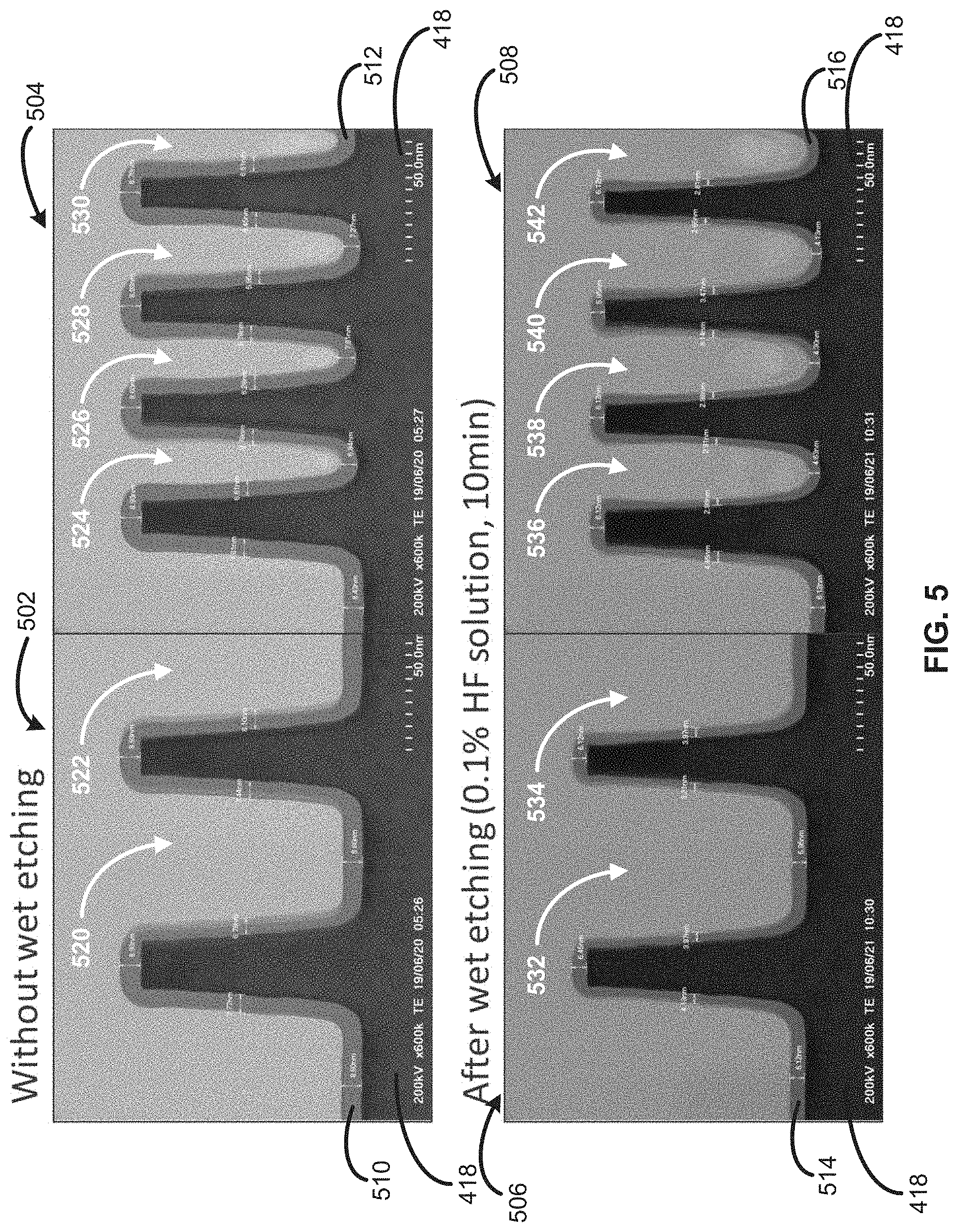
[0015] FIG. 2 illustrates another method in accordance with at least one embodiment of the disclosure.
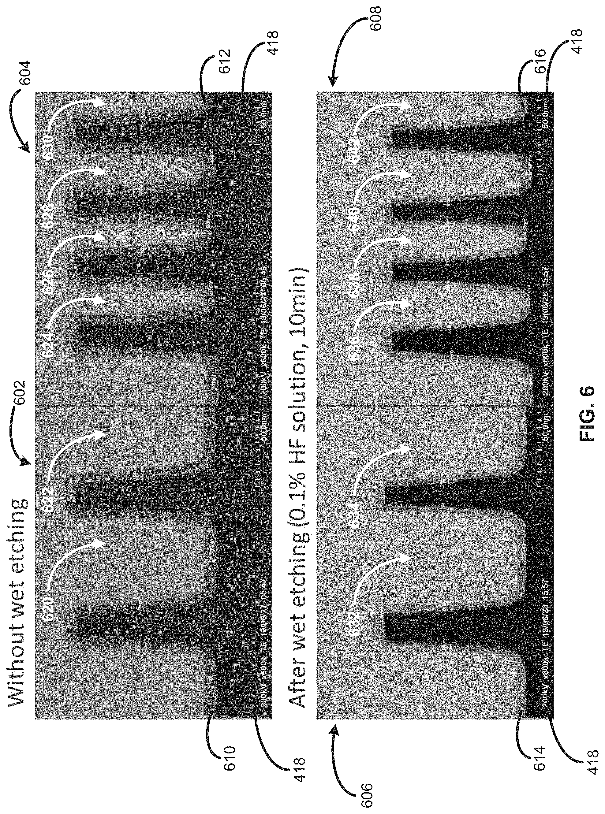
[0016] FIG. 3 illustrates a reactor system in accordance with at least one embodiment of the disclosure.
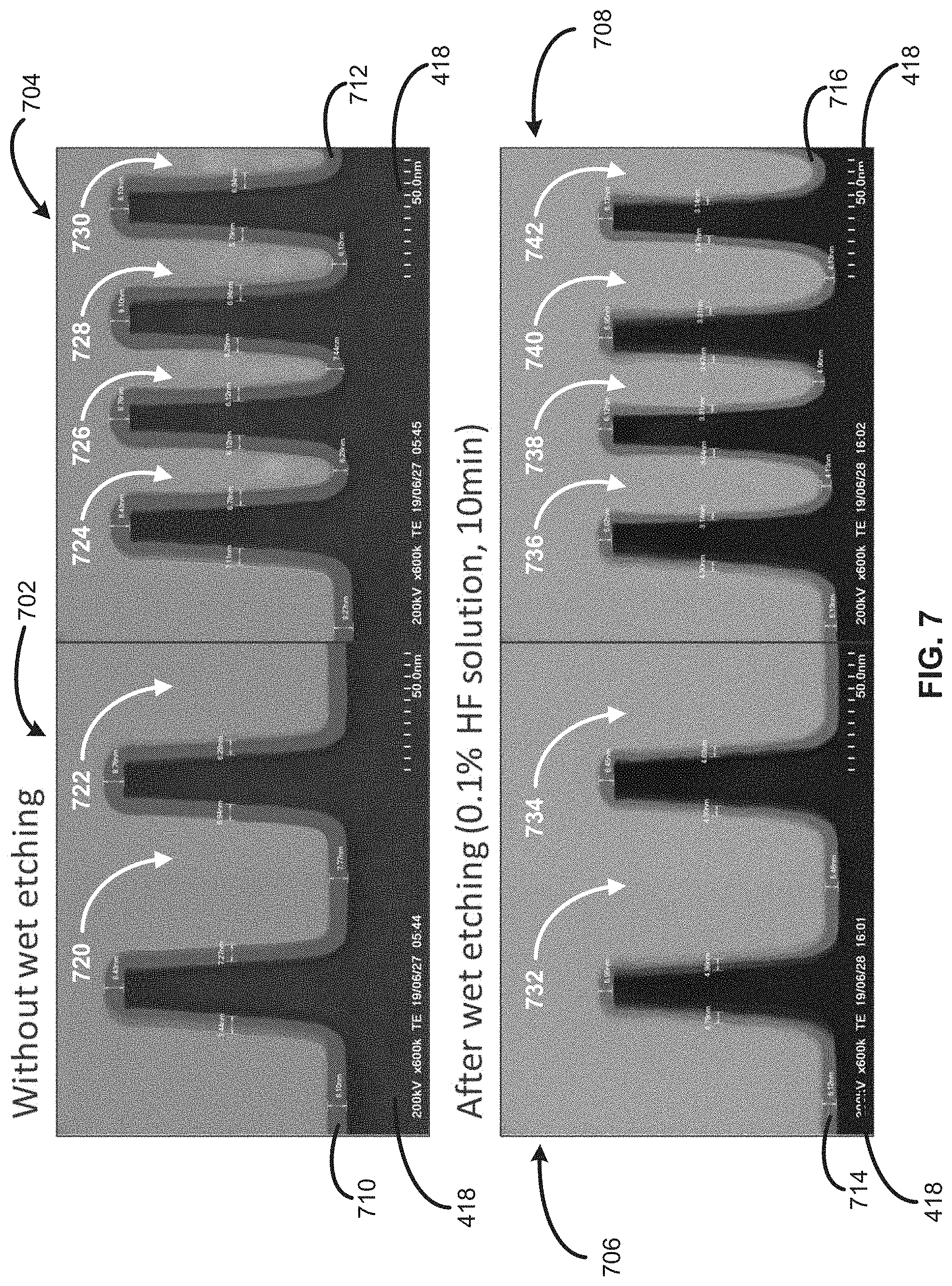
[0017] FIGS. 4-7 illustrate structures in accordance with exemplary embodiments of the disclosure.
[0018] FIG. 8 illustrates a relationship between wet etching time in 0.1% hydrofluoric acid vs etching depth of hydrogen neutral beam-irradiated NBEALD silicon oxide films.
[0019] It will be appreciated that elements in the figures are illustrated for simplicity and clarity and have not necessarily been drawn to scale. For example, the dimensions of some of the elements in the figures may be exaggerated relative to other elements to help improve understanding of illustrated embodiments of the present disclosure.
DETAILED DESCRIPTION OF EXEMPLARY EMBODIMENTS
[0020] Although certain embodiments and examples are disclosed below, it will be understood by those in the art that the invention extends beyond the specifically disclosed embodiments and/or uses of the invention and obvious modifications and equivalents thereof. Thus, it is intended that the scope of the invention disclosed should not be limited by the particular disclosed embodiments described below.
[0021] The present disclosure generally relates to methods of forming structures, such as structures suitable for forming electronic devices, to reactor systems for performing the methods, and to structures formed using the methods. By way of examples, the systems and methods described herein can be used to form conformal, high-quality insulating or dielectric layers. The insulating or dielectric layers can be deposited onto a surface of a substrate, which can include high-aspect ratio features. In some cases, the layers can be formed using a cyclic process that employs a neutral beam, such as NBEALD. In some cases, the layers can additionally or alternatively be exposed to (i.e., treated with) activated species formed using a neutral beam to form a structure including high-quality layers.
[0022] In this disclosure, "gas" may include material that is a gas at room temperature and pressure, a vaporized solid and/or a vaporized liquid, and may be constituted by a single gas or a mixture of gases, depending on the context. A gas other than the process gas, i.e., a gas introduced without passing through a gas distribution assembly, such as a showerhead, other gas distribution device, or the like, may be used for, e.g., sealing the reaction space, and may include a seal gas, such as a rare gas. In some embodiments, the term "precursor" can refer to a compound that participates in the chemical reaction that produces another compound, and particularly to a compound that constitutes a film matrix or a main skeleton of a film; the term "reactant" can refer to a compound, other than precursors, that activates a precursor, modifies a precursor, or catalyzes a reaction of a precursor, wherein the reactant may provide an element (such as O, N, or C) to a film matrix and become a part of the film matrix, when, for example, RF power is applied. The term "inert gas" can refer to a gas that does not take part in a chemical reaction and/or a gas that excites a precursor when RF power is applied, but unlike a reactant, it may not become a part of a film matrix to an appreciable extent. Exemplary inert gases include He, Ar, N.sub.2 and any combination thereof.
[0023] As used herein, the term "substrate" may refer to any underlying material or materials that may be used to form, or upon which, a device, a circuit, or a film may be formed. A substrate can include a bulk material, such as silicon (e.g., single-crystal silicon), other Group IV materials, such as germanium, or compound semiconductor materials, such as a Group II-VI or Group III-V semiconductor, and can include one or more layers overlying or underlying the bulk material. Further, the substrate can include various features, such as recesses, lines, and the like formed within or on at least a portion of a layer of the substrate. The feature can have relatively high aspect ratios, ranging from, for example, about 1 to about 50 or about 3 to about 20.
[0024] As used herein, the term "film" and/or "layer" can refer to any continuous or non-continuous structures and material, such as material deposited and/or treated by the methods disclosed herein. For example, film and/or layer can include two-dimensional materials, three-dimensional materials, nanorods, nanotubes, or nanoparticles or even partial or full molecular layers or partial or full atomic layers or clusters of atoms and/or molecules. A film or layer may comprise material or a layer with pinholes, which may be at least partially continuous.
[0025] As used herein, the term "cyclic deposition" can refer to the sequential introduction of precursors (reactants) into a reaction chamber to deposit a film over a substrate and includes deposition techniques, such as atomic layer deposition and cyclical chemical vapor deposition.
[0026] As used herein, the term "cyclical chemical vapor deposition" can refer to any process wherein a substrate is sequentially exposed to two or more volatile precursors, which react and/or decompose on a substrate to produce a desired deposition.
[0027] As used herein, the term "atomic layer deposition" (ALD) can refer to a vapor deposition process in which deposition cycles, typically a plurality of consecutive deposition cycles, are conducted in a reaction chamber. Typically, during each cycle, the precursor is chemisorbed to a deposition surface (e.g., a substrate surface or a previously deposited underlying surface such as material from a previous ALD cycle), forming a monolayer or sub-monolayer that does not readily react with additional precursor (i.e., a self-limiting reaction). Thereafter, a reactant (e.g., another precursor or reaction gas) may subsequently be introduced into the reaction chamber for use in converting the chemisorbed precursor to the desired material on the deposition surface. Typically, this reactant is capable of further reaction with the precursor. Further, purging steps may also be utilized during each cycle to remove excess precursor from the reaction chamber and/or remove excess reactant and/or reaction byproducts from the reaction chamber after conversion of the chemisorbed precursor. Further, the term "atomic layer deposition," as used herein, is also meant to include processes designated by related terms, such as chemical vapor atomic layer deposition, atomic layer epitaxy (ALE), molecular beam epitaxy (MBE), gas source MBE, or organometallic MBE, and chemical beam epitaxy when performed with alternating pulses of precursor composition(s), reactive gas, and purge (e.g., inert carrier) gas. PEALD refers to an ALD process, in which a plasma is applied during one or more of the ALD steps.
[0028] As used here, a "structure" can include a substrate as described herein. Structures can include one or more layers, overlying the substrate, which formed and/or treated as described herein.
[0029] Further, in this disclosure, any two numbers of a variable can constitute a workable range of the variable, and any ranges indicated may include or exclude the endpoints. Additionally, any values of variables indicated (regardless of whether they are indicated with "about" or not) may refer to precise values or approximate values and include equivalents, and may refer to average, median, representative, majority, etc. in some embodiments. Further, in this disclosure, the terms "including," "constituted by" and "having" refer independently to "typically or broadly comprising," "comprising," "consisting essentially of," or "consisting of" in some embodiments. In this disclosure, any defined meanings do not necessarily exclude ordinary and customary meanings in some embodiments.
[0030] In this disclosure, "continuously" can refer to one or more of without breaking a vacuum, without interruption as a timeline, without any material intervening step, without changing treatment conditions, immediately thereafter, as a next step, or without an intervening discrete physical or chemical structure between two structures other than the two structures in some embodiments.
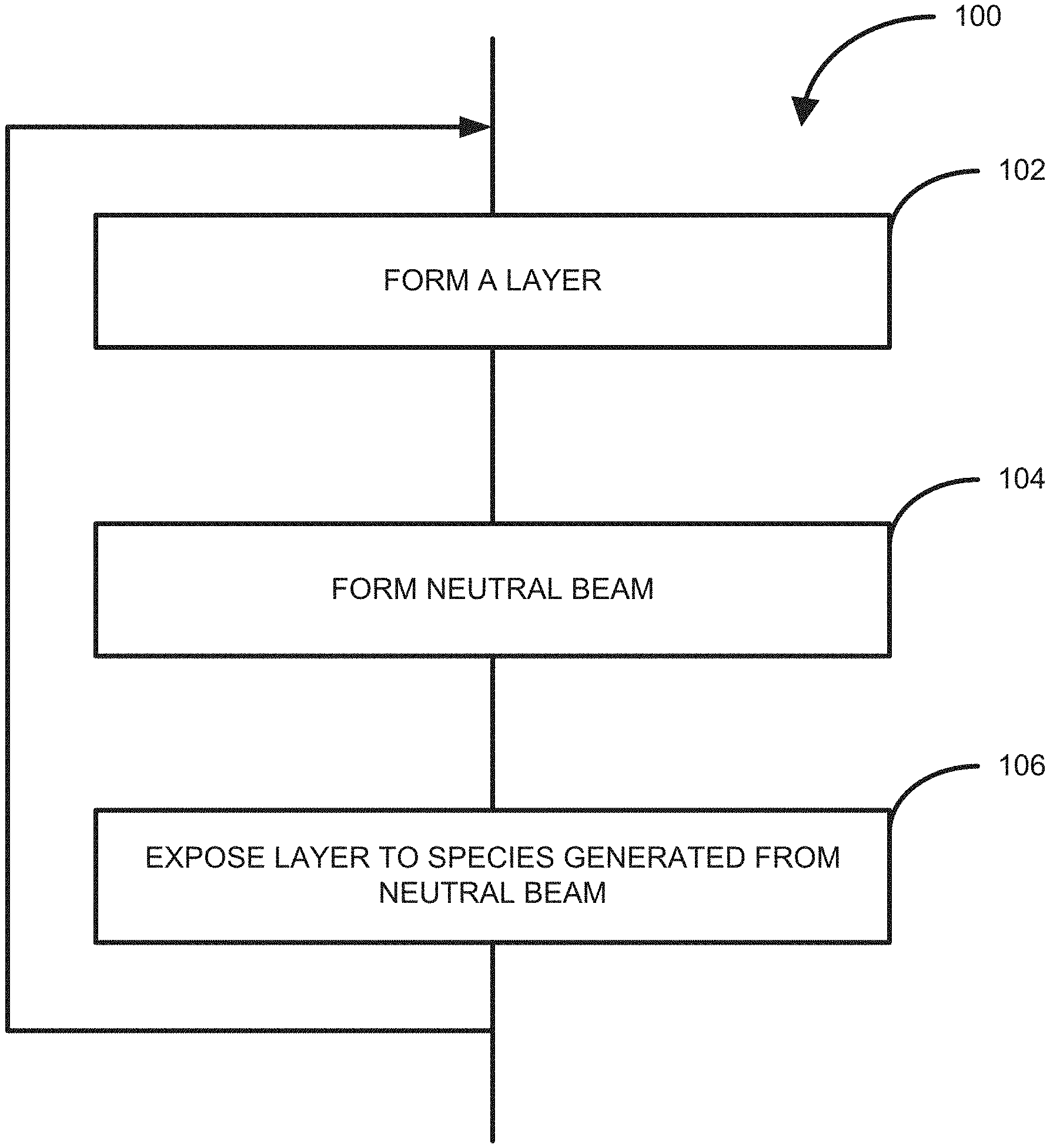
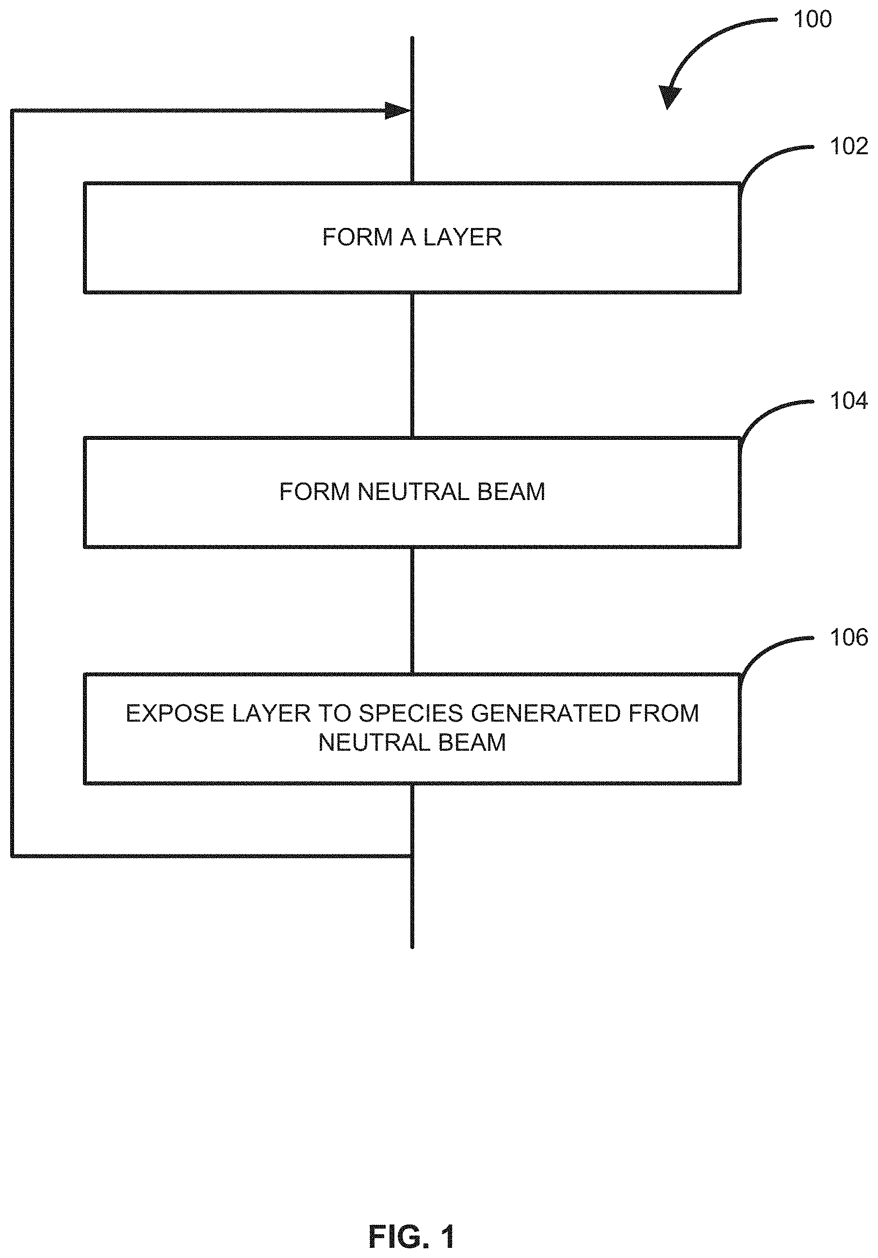
[0031] Turning now to the figures, FIG. 1 illustrates a method 100 of forming a structure in accordance with at least one embodiment of the disclosure. Method 100 includes the steps of forming a layer (step 102), forming a neutral beam (step 104), and exposing the layer to species generated from the neutral beam (step 106).
[0032] Step 102 can include forming an insulating or dielectric material layer. For example, step 102 can include forming one or more of an oxide, a nitride, and a carbide layer. By way of particular examples, the layer can be or include one or more of SiO.sub.2, SiN, SiOC, SiCN, SiC, SiON, SiOCN, SiBN, SiBO, GeO.sub.x, GeN, AlO.sub.X, TiO.sub.2, and TaO.sub.2. The layer can be formed using one or more of ALD, CVD, PEALD, PECVD, neutral beam enhanced ALD (NBEALD), and neutral beam enhanced CVD (NBECVD), for example, one or more of PEALD, PECVD, NBEALD, and NBECVD, or one or more of NBEALD and NBECVD.
[0033] A temperature within a reaction chamber during step 102 may be relatively low. For example, a temperature can be less than 400.degree. C., less than 300.degree. C., less than 200.degree. C., less than 100.degree. C., about 25-40.degree. C., about ambient temperature, about 0 to about 100.degree. C., about 0 to about 200.degree. C., or about 0 to about 300.degree. C. A pressure within the reaction chamber can be between about 0.01 Pa and about 100 Pa, about 0.05 Pa and about 1 Pa, or about 0.1 Pa and about 0.5 Pa.
[0034] In some cases, step 102 can include a plasma-enhanced deposition process. The plasma can be formed in a plasma chamber. When step 102 includes a plasma-enhanced deposition process, a power of an RF generator used to form the plasma can be between about 0.1 W/cm.sup.2 and about 20 W/cm.sup.2, about 0.2 W/cm.sup.2 and about 10 W/cm.sup.2, or about 1 W/cm.sup.2 and about 5 W/cm.sup.2. When the plasma is formed within a plasma chamber, a bias can be applied to, for example, an aperture plate of a neutral beam apparatus. The bias can be between about 0 W/cm.sup.2 and about 3 W/cm.sup.2, about 0 W/cm.sup.2 and about 1 W/cm.sup.2, or about 0 W/cm.sup.2 and about 0.5 W/cm.sup.2.
[0035] In some cases, step 102 includes a cyclic deposition process, such as one or more of PEALD, PECVD, NBEALD, and NBCVD. In these cases, step 102 can be repeated or can include repeating a number of cycles to form a layer of desired thickness. For example, a layer having a thickness of greater than zero and less than 10 nm can be formed during step 102.
[0036] In accordance with further examples of the disclosure, the layer formed during step 102 includes silicon. In these cases, a precursor used to form the layer can selected from the group consisting of aminosilanes, such as BDEAS (SiH.sub.2[N(C.sub.2H.sub.5).sub.2].sub.2), BTBAS (SiH.sub.2[NHC(CH.sub.3).sub.3].sub.2), TDMAS (SiH[N(CH.sub.3).sub.2].sub.3), HEAD (Si.sub.2[NHC.sub.2H.sub.6].sub.6), 3DMASCl (Si[N(CH.sub.3).sub.2].sub.3Cl), 3EMAS (H.sub.2Si[N(C.sub.2H.sub.5)CH.sub.3].sub.3), 4DMAS (Si[N(C.sub.2H.sub.6).sub.2]).sub.4), 4DEAS (Si[N(C.sub.2H.sub.6).sub.2].sub.4), and other Si-containing precursors, such as 4MS ((CH.sub.3).sub.4Si), 2ES ((C.sub.2H.sub.5).sub.2SiH.sub.2), phenyl-SiH.sub.3, cyclohexyl-SiH.sub.3, Si(OC.sub.2H.sub.5).sub.4. Additionally or alternatively, the reactant (e.g., an oxidant) can be selected from one or more of oxygen, CO, CO.sub.2, and NO.sub.2.
[0037] During step 104, a neutral beam is generated by introducing a gas to a plasma chamber, forming activated species within the plasma chamber, and passing the activated species through an aperture plate of a neutral beam apparatus to generate the neutral beam. In accordance with exemplary aspects of these embodiments, the neutral beam can be generated from one or more gases selected from the group consisting a of hydrogen-containing gases (e.g., hydrogen), He, NH.sub.3, O.sub.2, N.sub.2O, CO.sub.2, Ar, Xe, N.sub.2, and their mixture, such as one or more of H.sub.2 and He, and particularly H.sub.2. By way of particular examples, the neutral beam can be generated from one or more hydrogen-containing gases (e.g., H.sub.2) and helium. In these cases, the gas can include about 1 to about 100, about 10 to about 100, or about 90 to about 100 percent hydrogen and about 1 to about 100, about 10 to about 100, or about 90 to about 100 percent helium.
[0038] During step 106, the layer formed during step 102 is exposed to species generated from the neutral beam during step 104. Although separately illustrated, steps 104 and 106 can overlap and/or occur substantially at the same time. That is, as species are formed (e.g., within a plasma chamber) during step 104, the (e.g., activated) species can be introduced to the reaction chamber (e.g., through the aperture plate), such that the layer is exposed to the species generated from the neutral beam.
[0039] A temperature within a reaction chamber during steps 104 and/or 106 may be relatively low. For example, a temperature can be less than 400.degree. C., less than 300.degree. C., less than 200.degree. C., less than 100.degree. C., about 25-40.degree. C., about ambient temperature, about 0 to about 100.degree. C., about 0 to about 200.degree. C., or about 0 to about 300.degree. C. A pressure within the reaction chamber can be between about 0.01 Pa and about 100 Pa, about 0.05 Pa and about 1 Pa, or about 0.1 Pa and about 2 Pa.
[0040] During step 106, a bias can be applied to an aperture plate of an aperture plate of a neutral beam apparatus during the step of exposing the layer. By way of examples, the bias can range from about 0 W/cm.sup.2 to about 3 W/cm.sup.2, about 0 W/cm.sup.2 to about 1 W/cm.sup.2, or about 0.05 W/cm.sup.2 to about 0.2 W/cm.sup.2.
[0041] A power of an RF generator used to form the plasma during step 106 can be between about 0.1 W/cm.sup.2 and about 20 W/cm.sup.2, about 1 W/cm.sup.2 and about 15 W/cm.sup.2, or about 3 W/cm.sup.2 and about 10 W/cm.sup.2.
[0042] In accordance with exemplary aspects of these embodiments, steps 102-106 can be performed within the same reaction chamber.
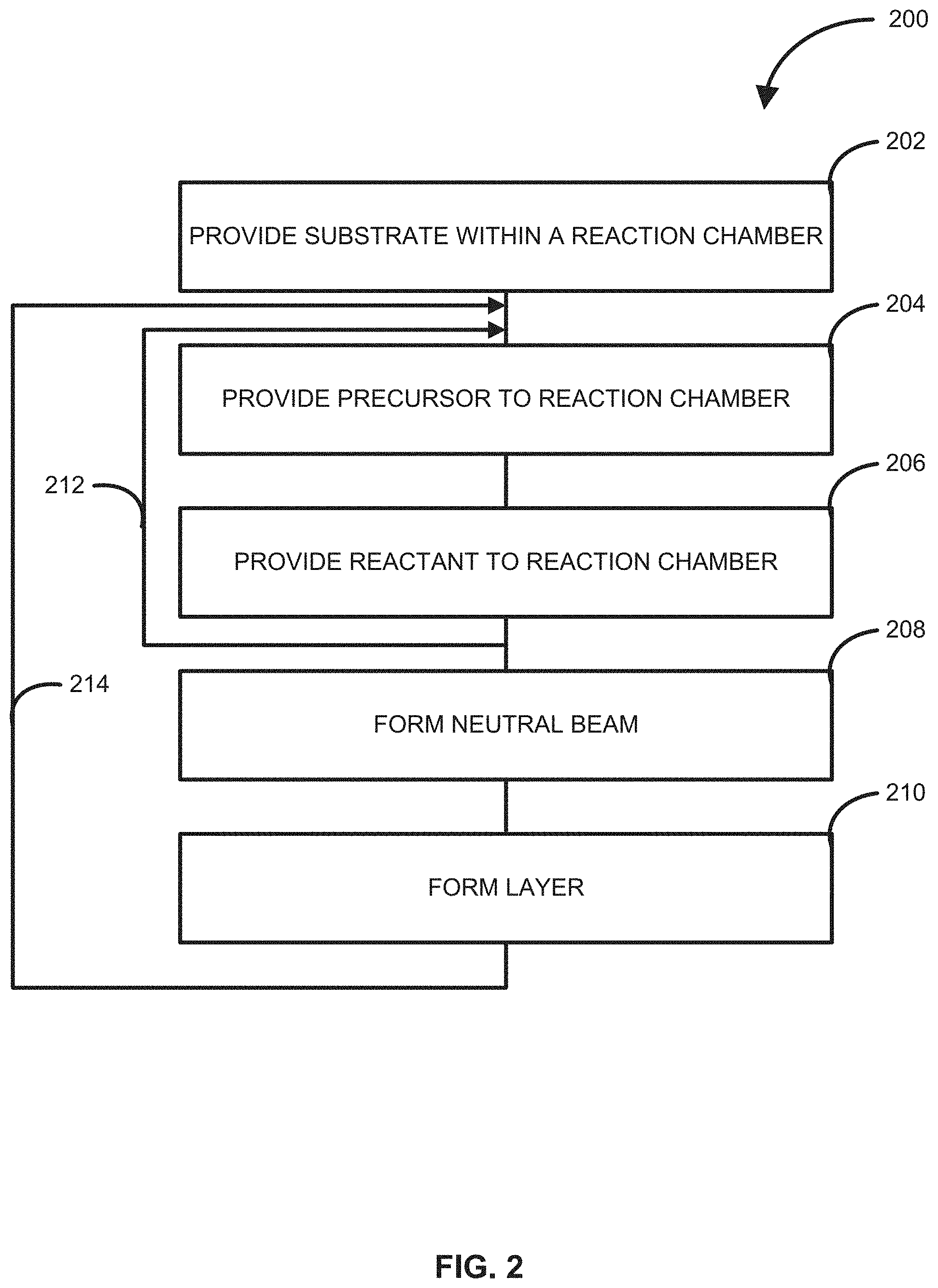
[0043] FIG. 2 illustrates another method 200 in accordance with exemplary embodiments of the disclosure. Method 200 includes the steps of providing a substrate within a reaction chamber (step 202), providing a precursor of the reaction chamber to form adsorbed species on a surface of the substrate (step 204), providing a reactant to a plasma chamber (step 206), forming a neutral beam from species generated in the plasma chamber (step 208), and exposing the adsorbed species to species from the neutral beam to form a layer comprising silicon (step 210).
[0044] During step 202, a substrate is provided within a reaction chamber. The reaction chamber can form part of one or more of an ALD, CVD, PEALD, PECVD, NBEALD, and NBECVD reactor system. For example, the reaction chamber can form part of one or more of PEALD, PECVD, NBEALD and NBECVD reactor system or one or more of NBEALD and NBECVD reactor system. Exemplary reactor systems can include one or more reaction chambers.
[0045] During step 202, a substrate or a susceptor upon which a substrate is placed, can be brought to a desired temperature. For example, the susceptor can be brought to a temperature of less than 400.degree. C., less than 300.degree. C., less than 200.degree. C., less than 100.degree. C., about 25-40.degree. C., about ambient temperature, about 0 to about 100.degree. C., about 0 to about 200.degree. C., or about 0 to about 300.degree. C. A pressure within the reaction chamber during step 202 can be brought to between about 0.01 Pa and about 100 Pa, about 0.05 Pa and about 1 Pa, or about 0.1 Pa and about 0.5 Pa.
[0046] During step 204, a precursor is provided to a gas inlet of the reaction chamber. The precursor can react with species on a surface of a substrate to form adsorbed species on the surface of the substrate. In accordance with examples of the disclosure, the precursor is selected from the group consisting of aminosilanes, such as BDEAS (SiH.sub.2[N(C.sub.2H.sub.5).sub.2].sub.2), BTBAS (SiH.sub.2[NHC(CH.sub.3).sub.3].sub.2), TDMAS (SiH[N(CH.sub.3).sub.2].sub.3), HEAD (Si.sub.2[NHC.sub.2H.sub.6].sub.6), 3DMASCl (Si[N(CH.sub.3).sub.2].sub.3Cl), 3EMAS (H.sub.2Si[N(C.sub.2H.sub.5)CH.sub.3].sub.3), 4DMAS (Si[N(C.sub.2H.sub.6).sub.2]).sub.4), 4DEAS (Si[N(C.sub.2H.sub.6).sub.2].sub.4), and other Si-containing precursors, such as 4MS ((CH.sub.3)4Si), 2ES ((C.sub.2H.sub.5).sub.2SiH.sub.2), phenyl-SiH.sub.3, cyclohexyl-SiH.sub.3, and Si(OC.sub.2H.sub.5).sub.4.
[0047] A flowrate of the precursor, alone or diluted with a carrier (e.g., an inert gas) to the reaction chamber can range from about 1 sccm to about 50 sccm, about 2 sccm to about 20 sccm, or about 4 sccm to about 10 sccm.
[0048] During step 204, a substrate or a susceptor upon which a substrate is placed, can be brought to or maintained at a desired temperature, such as a temperature set forth above in connections with step 202. A pressure within the reaction chamber can be the same or similar to the pressure recited above in connection with step 202.
[0049] During step 206, a reactant is provided to a gas inlet of a plasma chamber. Exemplary reactants include one or more of oxygen, CO, CO.sub.2, and NO.sub.2, which can be provided to the inlet of the plasma chamber alone, or in combination with a carrier gas. A flowrate of the reactant gas can range between about 10 sccm and about 3000 sccm, about 20 sccm and about 1000 sccm, or about 30 sccm and about 50 sccm.
[0050] During step 206, activated species can be generated from the reactant. In these cases, a bias can be applied to an aperture plate of a neutral beam apparatus during step 206. The bias can be between about 0 W/cm.sup.2 and about 3 W/cm.sup.2, about 0 W/cm.sup.2 and about 1 W/cm.sup.2, or about 0 W/cm.sup.2 and about 0.5 W/cm.sup.2.
[0051] Although illustrated with step 204 preceding step 206, in some cases, step 206 can precede step 204. In other words, the substrate can be contacted with a reactant first and then a precursor.
[0052] As illustrated, steps 204 and 206 can be repeated, as illustrated by loop 212. For example, steps 204 and 206 can be repeated a number of time until a desired thickness of material is deposited. In some cases, the desired thickness is less than 10 nm.
[0053] During step 208, activated species from a neutral beam are formed. The conditions and reactants for step 208 can be the same or similar to the conditions and reactants described above in connection with step 104. By way of example, step 208 can include providing gas comprising one or more of a such as one or more of a of hydrogen-containing gases (e.g., hydrogen), He, NH.sub.3, O.sub.2, N.sub.2O, CO.sub.2, Ar, Xe, N.sub.2, and their mixture, such as one or more of H.sub.2 and He, and particularly H.sub.2 to the plasma chamber and exposing the layer to species generated from the gas comprising one or more of a such as one or more of a of hydrogen-containing gases (e.g., hydrogen), He, NH.sub.3, O.sub.2, N.sub.2O, CO.sub.2, Ar, Xe, N.sub.2, and their mixture.
[0054] Similarly, the conditions and reactants for step 210 can be the same or similar to the conditions and reactants described above in connection with step 106. For example, a bias applied to an aperture plate of a neutral beam apparatus during the step of exposing the layer can be between about 0 W/cm.sup.2 and about 3 W/cm.sup.2, about 0 W/cm.sup.2 and about 1 W/cm.sup.2, or about 0.05 W/cm.sup.2 and about 0.2 W/cm.sup.2.
[0055] Steps 204-210, including loop 212, can be repeated until a layer of desired thickness is obtained, as illustrated by loop 214. The thickness can be greater than 10 nm.
[0056] FIG. 3 illustrates a cross-sectional view of a reactor system 300 in accordance with exemplary embodiments of the disclosure. Reactor system 300 can be configured to perform the steps according to methods described herein.
[0057] In the illustrated example, reactor system 300 includes a reactor 302 including a reaction chamber 304, a susceptor 306, a plasma chamber 308, an aperture plate 310, antenna 312, a plasma generation power source 314, and a bias power source 316. Reactor system 300 can also include a precursor gas inlet 318, a reactant gas inlet 320, and an outlet 322, and a controller 328.
[0058] Reactor 302 can include any suitable gas-phase reactor. Exemplary reactors include ALD reactors and CVD reactors, such as those available in systems provided by ASM International.
[0059] Susceptor 306 can be capable of moving vertically to load and unload a substrate 324. Lift pins and a robot arm (not shown) can be used to load and unload the substrate from the surface of susceptor 306.
[0060] Plasma chamber 308 includes an interior region 326 that is in is in fluid communication with reaction chamber 304. Plasma generation power source 314 and antenna 312 can be used to provide, for example, provide radio frequency (RF) power within plasma chamber 308. The RF power can be used to form a plasma that includes activated species generated from gas (e.g., reactant gas and/or gas used for treatment of a layer) provided to interior region using, for example, reactant gas inlet 320. Plasma chamber 308 can form part of an inductively coupled plasma (ICP), a capacitively coupled plasma (CCP), electron cyclotron resonance (ECR), surface-wave-sustained discharge (SWP), or neutral loop discharge (NLD) plasma apparatus.
[0061] Aperture plate 310 can be used to neutralize the activated species formed within plasma chamber 308 prior to activated species entering reaction chamber 304. To facilitate flow of activated species from plasma chamber 304 toward susceptor 306 and/or substrate 324, bias power source 316 can be used to apply a bias voltage to aperture plate 310 to attract ionized species formed within a plasma. Activated species, even though neutralized by aperture plate 310 can continue to flow toward substrate 324 due, at least in part, to the kinetic energy of the species.
[0062] Aperture plate 310 can be formed of an electric conductor, such as graphite. Aperture plate 310 can include a plurality of apertures, which can be configured in, for example, a hexagonal configuration.
[0063] Precursor gas inlet 318 is used to introduce a precursor gas and/or a purge gas into reaction chamber 304. Although only one precursor gas inlet 318 is illustrated, reactor system 300 can include more than one precursor gas inlet 318. For example, multiple precursor gas inlets can be used to introduce one or more precursors to reaction chamber 304 and/or one or more precursors and one or more purge gases to reaction chamber 304.
[0064] Reactant gas inlet 320 is used to introduce a reactant gas and/or a treatment gas into interior region 326 of plasma chamber 308. Although only one reactant gas inlet 320 is illustrated, reactor system 300 can include more than one reactant gas inlet 320.
[0065] Controller 328 can include one or more devices to control power to plasma generation power source 314 and/or bias power source 316. Controller 328 can also be used to control flow of gases--e.g., one or more gases to precursor gas inlet 318 and/or reactant gas inlet 320, control pressure within reaction chamber 304, control pressure within plasma chamber 308, and the like. For example, a pressure within reaction chamber 304 can be controlled by controlling flowrate(s) of gas(es) into reaction chamber 304 and/or plasma chamber 308 and controlling flow through outlet 322. In accordance with various examples of the disclosure, controller 328 is configured to have system 300 perform methods as described herein.
[0066] In accordance with additional examples of the disclosure, a structure, such as a structure illustrated in FIGS. 4-7 is provided. The structure can include a substrate and a layer deposited thereon. Exemplary deposition and treatment conditions for depositing and treating a layer are provide below in the examples.
EXAMPLES
[0067] The examples provided below are meant to be illustrative. Unless otherwise noted, embodiments of the disclosure are not limited to the specific examples provided below.
Example 1
[0068] For the structures formed according to example 1, an NBEALD process was used to deposit a layer onto a substrate. Here, a neutral beam apparatus with 20-cm-diameter aperture plate was used. The NBEALD process included cyclic repeat of following steps: (1) supplying precursor (aminosilane) to process a chamber and adsorption of the precursor on a substrate, (2) stopping a flow of the precursor supply to the reaction chamber, (3) supplying a reactant (e.g., oxidant) gas to a plasma chamber, (4) generating a neutral beam from the reactant gas and providing activated species from the neutral beam to the substrate, and (5) stopping generation of neutral beam and reactant gas supply. Table 1 shows detail of NBEALD conditions used in example 1.
TABLE-US-00001 TABLE 1 NBEALD conditions. Value in this Parameter example Range Precursor gas Aminosilane 5 sccm Aminosilane 1-50 supply sccm; carrier gas (e.g., He, Ar, and/or N.sub.2) may be used Oxidant gas O.sub.2 30 sccm One or plural of supply oxidizing gas (e.g., O.sub.2, CO, CO.sub.2, or NO.sub.2) and none, one, or plural of inert gas (e.g., He, Ar, N.sub.2), 10-3000 sccm Type of plasma ICP ICP, CCP, ECR, SWP, NLD generator Frequency of 13.56 MHz 400 kHz-3 GHz plasma generation RF power source Power of plasma 1000 W (3.2 W/cm.sup.2) 0.1 W/cm2-20 W/cm.sup.2 generation RF power source Pressure of 0.11 Pa 0.01-100 Pa reaction chamber during neutral beam irradiation Pressure of 0.41 Pa Any pressure which can plasma chamber generate plasma during neutral (depending on plasma beam irradiation type) Number of cycles 90 any number, depending on desired thickness Frequency of bias 150 kHz 50-2000 kHz RF power source Power of bias RF 0 or 100 W (0 or 0-3 W/cm.sup.2 power source 0.32 W/cm.sup.2) Stage temperature 30.degree. C. 0-100.degree. C., or 0-200.degree. C., or 0-300.degree. C.
[0069] After formation of the film, a hydrogen neutral beam was irradiated to the sample using the same apparatus without transferring the sample. The condition for the neutral beam treatment of the film is shown in Table 2.
TABLE-US-00002 TABLE 2 Hydrogen neutral beam irradiation condition. Value in Parameter example 1 Range Gas supply Hydrogen 75 sccm H2, He, NH.sub.3, O.sub.2, N.sub.2O, CO.sub.2, Ar, Xe, N.sub.2, and their mixture gas, preferably H.sub.2 or He, more preferably H.sub.2, 10-3000 sccm Type of plasma ICP ICP, CCP, ECR, generator SWP, NLD Frequency of 13.56 MHz 400 kHz-3 GHz plasma generation RF power Power of plasma 1300 W (4.1 W/cm.sup.2) 0.1 W/cm2-20 W/cm.sup.2 generation RF power Frequency of 150 kHz 50-2000 kHz bias RF power Power of bias 0, 20, 40, 60 W (0, 0.064, 0-0.5 W/cm.sup.2, RF power 0.127, 0.191 W/cm.sup.2) preferably 0.08-0.16 W/cm.sup.2 Pressure of 1.1 Pa 0.01-100 Pa reaction chamber Pressure of 1.8 Pa Any pressure which can plasma chamber generate plasma (depending on plasma type) Irradiation time 10-40 minutes 10 seconds or more Stage temperature 30.degree. C. 0-100.degree. C., 0-200.degree. C., 0-300.degree. C., or room temperature
[0070] WER (wet etch rates) for layers deposited according to the conditions set forth above in 0.1% hydrofluoric acid were measured. The WER results are shown in Table 3. Data for a plasma ALD film and a thermal oxide film are also shown in Table 3. As shown, WER of NBEALD film (10 nm) was decreased from 1.39 nm/min to 0.39, 0.37, 0.30 nm/min by hydrogen neutral beam irradiation without bias of 10, 25, 40 minutes. These values correspond to wet etch rate ratios (WERR) of 1.63, 1.54, 1.25. These values are even lower than high temperature (390.degree. C.) PEALD (0.43 nm/min).
[0071] Bias application during hydrogen neutral beam irradiation was also tested and results are shown in Table 3. Without bias, WERR was 1.25. By applying 20 and 40 W bias, WERR was improved (decreased) to 1.21 and 1.17. However, by applying 60 W bias, WERR was increased to 1.67. Note that this value is still smaller (better) than no-H.sub.2-neutral-beam-treatment result of 5.79. These results indicate that the best bias power, for the conditions set forth above, is 40 W.
[0072] Hydrogen plasma irradiation has been used to reform PEALD silicon oxide to reduce WER in 1:1000 (0.05%) HF down to 0.1 nm/min (top, side) and 0.2 nm/min (bottom). Since WER of thermal oxide in 1:1000 HF is about 0.04 nm/min, these results correspond WERR of 2.5-5. This means that hydrogen neutral beam irradiation can achieve lower WERR. There are several possible reasons why neutral beam obtained better results than plasma, including: (1) plasma (ion) irradiation causes charge-up of target film and prevents further introduction of coming ions, while neutral beam irradiation does not cause charge-up and (2) plasma irradiates strong ultraviolet light which may cause defect generation in target film, while neutral beam irradiates much less ultraviolet light and does not generate defects.
TABLE-US-00003 TABLE 3 WER and WERR (wet etch rate ratio against thermal oxide) of various silicon oxide films (with and without hydrogen neutral beam irradiation) formed on blanket silicon wafer. Deposition method thermal NBEALD PEALD SiO.sub.2 Deposition condition Bias No bias 100 W 390.degree. C. -- H.sub.2 neutral beam condition No No No Bias Bias Bias bias, bias, bias, 20 W, 40 W, 60 W, N/A 10 min 25 min 40 min 30 min 30 min 30 min N/A N/A N/A WER 1.39 0.39 0.37 0.30 0.29 0.28 0.40 1.01 0.43 0.24 (nm/min) WERR 5.79 1.63 1.54 1.25 1.21 1.17 1.67 4.21 1.79 --
[0073] Application of RF bias power (400 kHz, 100 W) can also decrease WER to 1.01 nm/min. However, hydrogen neutral beam irradiation can achieve much lower WER.
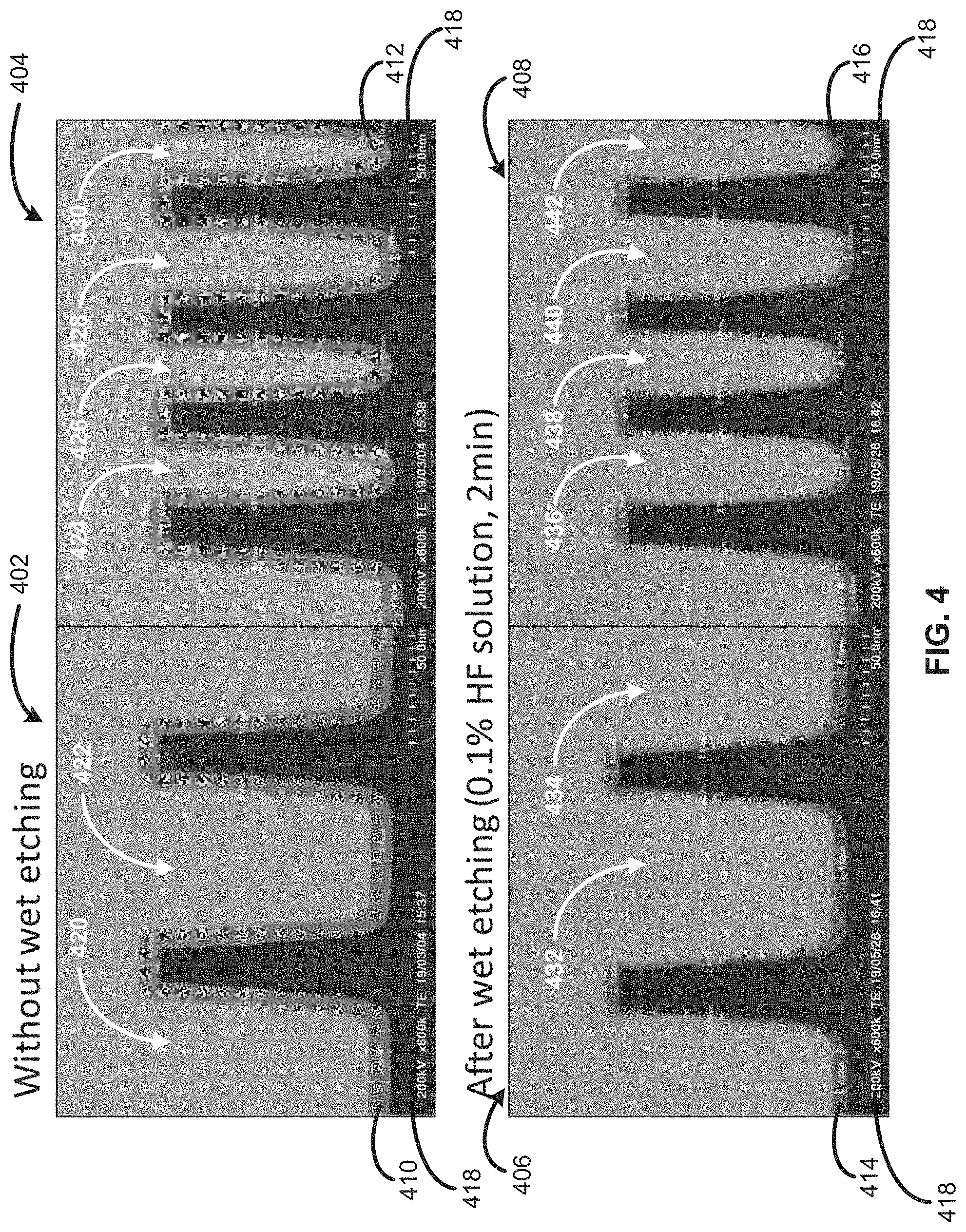
[0074] Wet etching using 0.1% hydrofluoric acid was applied also for trench pattern sample. FIG. 4-7 illustrate cross-sectional STEM images of structures 402-708, including layers deposited according to conditions set forth above, before and after wet etching.
[0075] FIG. 4 illustrates structure 402 having features 420, 422 formed within a substrate 418 and a layer 410 formed overlying substrate 418 and structure 404 having features 424-430 and a layer 412 overlying substrate 418--both without wet etching and structure 406 with features 432 and 434 and a layer 414 overlying substrate 418 and structure 408 having features 436-442 with a layer 416 overlying substrate 418--both with wet etching. No neutral beam irradiation was performed on the samples illustrated in FIG. 4.
[0076] FIG. 5 illustrates structure 502 having features 520, 522 formed within a substrate 418 and a layer 510 formed overlying substrate 418 and structure 504 having features 524-530 and a layer 512 overlying substrate 418--both without wet etching and structure 506 with features 532 and 534 and a layer 514 overlying substrate 418 and structure 508 having features 536-542 with a layer 516 overlying substrate 418--both after wet etching. Hydrogen neutral beam irradiation without bias was applied to the deposited material to form layers 510-516.
[0077] FIG. 6 illustrates structure 602 having features 620, 622 formed within a substrate 418 and a layer 610 formed overlying substrate 418 and structure 604 having features 624-630 and a layer 612 overlying substrate 418--both without wet etching and structure 606 with features 632 and 634 and a layer 614 overlying substrate 418 and structure 608 having features 636-642 with a layer 616 overlying substrate 418--both after wet etching. Hydrogen neutral beam irradiation with a bias of about 20 W was applied to the deposited material to form layers 610-616.
[0078] FIG. 7 illustrates structure 702 having features 720, 722 formed within a substrate 418 and a layer 710 formed overlying substrate 418 and structure 704 having features 724-730 and a layer 712 overlying substrate 418--both without wet etching and structure 706 with features 732 and 734 and a layer 714 overlying substrate 418 and structure 708 having features 736-742 with a layer 716 overlying substrate 418--both after wet etching. Hydrogen neutral beam irradiation with a bias of about 40 W was applied to the deposited material to form layers 710-716.
[0079] Table 4 summarizes the wet etching results of layers 410-416, 510-516, 610-616, and 710-716. As illustrated and as set forth in Table 4, WER of a feature (e.g., trench) sidewall, in addition to the WER of the top and bottom of the feature, is decreased by neutral beam irradiation. WERIR at different positions (top, side, bottom) are similar. This shows effect of H.sub.2--NB irradiation is isotropic (conformal). Indeed, WER-decreasing effect is even a bit stronger (larger WERIR) at sidewall than top and bottom. This may be because WER at sidewall is larger and there is larger margin for decrease of WER, while decrease of WER at top and bottom saturates. Also, this result shows that WER of bottom of trench pattern with relatively high aspect ratio of 3.3 was decreased with similar WERIR.
TABLE-US-00004 TABLE 4 WER and WERR of NBEALD silicon oxide with/without H.sub.2 NB deposited on trench pattern. w/o H.sub.2-NB H.sub.2-NB H.sub.2-NB H.sub.2-NB no bias bias 20 W bias 40 W WER top 1.68 0.27 0.24 0.23 (nm/min) side 2.42 0.35 0.29 0.27 bottom 1.77 0.26 0.26 0.21 WERR (--) top 8.16 1.31 1.18 1.11 side 11.76 1.70 1.43 1.33 bottom 8.58 1.25 1.28 1.04 WERIR (--) top -- 6.2 6.9 7.4 side -- 6.9 8.2 8.9 bottom -- 6.8 6.7 8.2 WER = wet etch rate WERR = wet etch rate ratio, WER(target)/WER(thermal oxide) WERIR = wet etch rate improvement ratio, WER(w/o H.sub.2-NB)/WER(target)
[0080] FIG. 8 shows relationship 800 between remaining film thickness and hydrofluoric acid etching time for 10 minutes (line 802), 25 minutes (lines 804), and 40 minutes (lines 806). The relationship was linear, at least, up to 20 minutes (6-8 nm depth). This means the effect of hydrogen neutral beam irradiation can reach at least 6-8 nm depth. By considering penetration depth of hydrogen plasma into silicon dioxide, the effect may reach up to about 10 nm depth. So, by repeating deposition of silicon oxide film by NBEALD (or other technique) to a thickness of less than 10 nm and exposing a formed layer to neutral beam treatment, high-quality silicon oxide film with thickness more than 10 nm can be obtained.
Example 2
[0081] For the structures formed according to example 2, SiO.sub.2 layers were deposited by PEALD onto a substrate. The substrate included planar surface and trench patterns. The deposition conditions for the PEALD layers are shown in Table 5.
TABLE-US-00005 TABLE 5 PEALD SiO.sub.2 deposition condition. Parameter Value in example 2 Precursor Aminosilane (carrier gas: Ar 2 slm) Gas supply O.sub.2 2 slm, Ar (carrier gas for precursor) 2 slm Pressure 400 Pa Frequency of plasma generation RF 13.56 MHz power Power of plasma generation RF 50 W (0.071 W/cm.sup.2) power Discharge time of plasma generation 1.2 s RF power for each ALD cycle State temperature 300.degree. C.
[0082] The deposited layers were then exposed to activated species from a helium neutral beam. Here, a neutral beam apparatus with 10-cm-diameter aperture plate was used. Irradiation conditions are shown in Table 6.
TABLE-US-00006 TABLE 6 Helium neutral beam irradiation condition. (Exemplary ranges of parameters are provided in Table 2, above.) Parameter Value in this example 2 Gas supply Helium 10-20 sccm Type of plasma generator ICP Frequency of plasma 13.56 MHz generation RF power Power of plasma generation 500 W (6.4 W/cm.sup.2) RF power Pressure of reaction 0.16-0.30 Pa chamber Pressure of plasma chamber Pa Irradiation time 5-40 minutes Stage temperature Room temperature or 200.degree. C.
[0083] WER of the treated layers in 0.25% hydrofluoric acid were measured. The WER are shown in Table 7. As a shown, WERR of the layer was decreased from 8.6 to 7.2, 5.1, 4.4, and 3.2 by helium neutral beam irradiation of 5, 10, 20, and 40 minutes at 300.degree. C. In case of room temperature, WERR was decreased from 8.6 to 6.8, 6.4, 6.1, and 4.1 by helium neutral beam irradiation of 5, 10, 20, and 40 minutes. It is shown that He neutral beam irradiation can decrease WER of silicon oxide, though, in the illustrative examples, the range of decrease is smaller than the rage of decrease obtained using H.sub.2 neutral beam irradiation.
TABLE-US-00007 TABLE 7 WERR of PEALD silicon oxide films with and without He neutral beam irradiation formed on blanket silicon wafer He flow 10 sccm 20 sccm Pressure 0.16 Pa 0.30 Pa Temperature 300.degree. C. (No Irradiation time irradiation) 5 min 10 min 20 min 40 min 20 min WERR 8.6 7.2 5.1 4.4 3.2 6.1 He flow 10 sccm 20 sccm Pressure 0.16 Pa 0.30 Pa Temperature Room temperature (No Irradiation time irradiation) 5 min 10 min 20 min 40 min 20 min WERR 8.6 6.8 6.4 6.1 4.1 6.5
[0084] Table 8 shows WERR of PEALD silicon oxide film deposited on top, side, bottom of trench structure. WERR of top, side, and bottom was decreased by helium neutral beam irradiation. In case of helium, WERIR of top is a bit larger than that of side and bottom, indicating that, for this illustrative example, He neutral beam irradiation may modify the top of structure more strongly than side and bottom surface, unlike H.sub.2 neutral beam irradiation.
TABLE-US-00008 TABLE 8 WERR of PEALD silicon oxide with/without He NB deposited on trench pattern. Values in parentheses show WERIR (WER improvement ratio). with He-NB without He-NB 300.degree. C., Room temperature, Position -- 20 minutes 20 minutes Top 9.9 3.75 (2.6) 5.63 (1.8) Side 8.9 4.13 (2.2) 6.13 (1.5) bottom 9.3 4.38 (2.1) 6.50 (1.4)
[0085] The example embodiments of the disclosure described above do not limit the scope of the invention, since these embodiments are merely examples of the embodiments of the invention. Any equivalent embodiments are intended to be within the scope of this invention. Indeed, various modifications of the disclosure, in addition to the embodiments shown and described herein, such as alternative useful combinations of the elements described, may become apparent to those skilled in the art from the description. Such modifications and embodiments are also intended to fall within the scope of the appended claims.
* * * * *
D00000
D00001
D00002
D00003
D00004
D00005
D00006
D00007
D00008
XML
uspto.report is an independent third-party trademark research tool that is not affiliated, endorsed, or sponsored by the United States Patent and Trademark Office (USPTO) or any other governmental organization. The information provided by uspto.report is based on publicly available data at the time of writing and is intended for informational purposes only.
While we strive to provide accurate and up-to-date information, we do not guarantee the accuracy, completeness, reliability, or suitability of the information displayed on this site. The use of this site is at your own risk. Any reliance you place on such information is therefore strictly at your own risk.
All official trademark data, including owner information, should be verified by visiting the official USPTO website at www.uspto.gov. This site is not intended to replace professional legal advice and should not be used as a substitute for consulting with a legal professional who is knowledgeable about trademark law.