STRUCTURE INCLUDING SiOC LAYER AND METHOD OF FORMING SAME
Sharma; Bed Prasad ; et al.
U.S. patent application number 16/800114 was filed with the patent office on 2020-09-10 for structure including sioc layer and method of forming same. The applicant listed for this patent is ASM IP Holding B.V.. Invention is credited to YoungChol Byun, Bed Prasad Sharma, Eric James Shero, Shankar Swaminathan.
| Application Number | 20200286725 16/800114 |
| Document ID | / |
| Family ID | 1000004675391 |
| Filed Date | 2020-09-10 |


| United States Patent Application | 20200286725 |
| Kind Code | A1 |
| Sharma; Bed Prasad ; et al. | September 10, 2020 |
STRUCTURE INCLUDING SiOC LAYER AND METHOD OF FORMING SAME
Abstract
A method for forming a layer comprising SiOC on a substrate is disclosed. An exemplary method includes selectively depositing a layer comprising silicon nitride on the first material relative to the second material and depositing the layer comprising SiOC overlying the layer comprising silicon nitride.
| Inventors: | Sharma; Bed Prasad; (Gilbert, AZ) ; Swaminathan; Shankar; (Phoenix, AZ) ; Byun; YoungChol; (Tempe, AZ) ; Shero; Eric James; (Phoenix, AZ) | ||||||||||
| Applicant: |
|
||||||||||
|---|---|---|---|---|---|---|---|---|---|---|---|
| Family ID: | 1000004675391 | ||||||||||
| Appl. No.: | 16/800114 | ||||||||||
| Filed: | February 25, 2020 |
Related U.S. Patent Documents
| Application Number | Filing Date | Patent Number | ||
|---|---|---|---|---|
| 62815810 | Mar 8, 2019 | |||
| Current U.S. Class: | 1/1 |
| Current CPC Class: | H01L 21/02274 20130101; C23C 16/36 20130101; H01L 21/022 20130101; H01L 21/0228 20130101; H01L 21/02211 20130101; C23C 28/04 20130101; H01L 21/0217 20130101; C23C 16/345 20130101; H01L 21/02126 20130101; C23C 16/45536 20130101 |
| International Class: | H01L 21/02 20060101 H01L021/02; C23C 28/04 20060101 C23C028/04; C23C 16/34 20060101 C23C016/34; C23C 16/455 20060101 C23C016/455; C23C 16/36 20060101 C23C016/36 |
Claims
1. A method of forming a structure, the method comprising the steps of: providing a substrate within a reaction chamber, the substrate comprising a surface comprising a first material and a second material, the first material comprising a metal and the second material comprising one or more of an oxide, a nitride, and an oxynitride; selectively depositing a layer comprising silicon nitride on the first material relative to the second material; and depositing a layer comprising SiOC overlying the layer comprising silicon nitride.
2. The method of claim 1, wherein the step of selectively depositing comprises atomic layer deposition.
3. The method of claim 1, wherein a temperature of a susceptor within the reaction chamber during the step of selectively depositing is between about 100.degree. C. and about 500.degree. C.
4. The method of claim 1, further comprising a step of exposing the layer comprising silicon nitride to a plasma treatment prior to the step of depositing a layer comprising SiOC.
5. The method of claim 4, wherein the step of exposing the layer comprising silicon nitride to a plasma treatment comprises exposing the layer comprising silicon nitride to a plasma comprising one or more of nitrogen and helium.
6. The method of claim 4, wherein the step of exposing the layer comprising silicon nitride to a plasma treatment and the step of depositing a layer comprising SiOC are performed within the same reaction chamber.
7. The method of claim 1, wherein the step of depositing a layer comprising SiOC comprises thermal atomic layer deposition.
8. The method of claim 1, wherein the step of depositing a layer comprising SiOC comprises plasma-enhanced atomic layer deposition.
9. The method of claim 8, wherein a power applied during the plasma-enhanced atomic layer deposition is between about 400 W and about 800 W.
10. The method of claim 8, wherein a pressure within the reaction chamber during the plasma-enhanced atomic layer deposition is between about 5 Torr and about 15 Torr.
11. The method of claim 1, wherein the layer comprising SiOC comprises SiOCN.
12. The method of claim 1, the step of depositing a layer comprising SiOC comprises providing a precursor comprising one or more of a methoxysilane, tetramethyl bis (2,2 dimethylhydrazine) disilane and (3-Mercaptopropyl)trimethoxysilane.
13. A structure formed according to the method of claim 1.
14. The structure of claim 13 comprising a spacer.
15. A method of forming a structure, the method comprising the steps of: providing a substrate within a reaction chamber, the substrate comprising a surface comprising a first material and a second material, the first material comprising an oxide and the second material comprising a nitride; and selectively depositing a layer comprising SiOC overlying the first material.
16. The method of claim 15, wherein the step of selectively depositing a layer comprising SiOC comprises plasma-enhanced atomic layer deposition.
17. The method of claim 16, wherein a power applied during the step of selectively depositing a layer comprising SiOC is between about 5 W and about 5000 W.
18. The method of claim 15, wherein a pressure within the reaction chamber during the step of selectively depositing a layer comprising SiOC is between about 5 Torr and about 15 Torr.
19. A structure formed according to the method of claim 15.
20. The structure of claim 19, wherein the layer comprising SiOC forms an etch stop cap layer of the structure.
Description
CROSS-REFERENCE TO RELATED APPLICATIONS
[0001] This application claims priority to and the benefit of U.S. Provisional Patent Application Ser. No. 62/815,810, filed Mar. 8, 2019 and entitled "STRUCTURE INCLUDING SiOC LAYER AND METHOD OF FORMING SAME," which is hereby incorporated by reference.
FIELD OF INVENTION
[0002] The present disclosure generally relates to methods of forming structures that include a layer comprising silicon, oxygen, and carbon and to structures including such layers.
BACKGROUND OF THE DISCLOSURE
[0003] Silicon nitride films are used for a wide variety of applications. For example, such films can be used as insulating layers, as etch stop layers, and for use in the formation of spacers in the formation of electronic devices.
[0004] For several applications, it may be desirable to selectively deposit silicon nitride on one material relative to another material. For example, it may be desirable to selectively deposit the silicon nitride material onto metal relative to dielectric material. Further, because of subsequent processing steps, it may be desirable for the silicon nitride material to be relatively resistant to wet etching processes, such as wet etching using hydrofluoric acid and/or hot phosphoric acid.
[0005] Low pressure chemical vapor deposition (LPCVD) techniques can be used to deposit silicon nitride films with relatively low wet etch rates. However, such films typically require relatively high temperatures for deposition, and the high temperatures may not be suitable for some applications. Plasma-enhance chemical vapor deposition (PECVD) techniques have also been used to deposit silicon nitride films; however, films formed using PECVD generally exhibit high wet etch rates.
[0006] Low-temperature CVD techniques have been developed for selectively depositing silicon nitride films on metal relative to surrounding dielectric. And, atomic layer deposition (ALD) techniques for depositing silicon nitride have been developed. Such techniques allow for deposition of films at lower temperatures and ALD has an advantage of depositing conformal films. However, the wet etch rates of such films tend to be relatively high.
[0007] Accordingly, improved methods for forming structures, such as structures including silicon nitride films, are desired.
SUMMARY OF THE DISCLOSURE
[0008] Various embodiments of the present disclosure relate to methods of forming structures, such as structures suitable for use in the manufacturing of electronic devices. While the ways in which various embodiments of the present disclosure address drawbacks of prior methods and structures are discussed in more detail below, in general, various embodiments of the disclosure provide improved structures that include a layer comprising silicon, oxygen, and carbon, which can be used to obtained desired etch-resistant properties, and to methods of forming such structures.
[0009] In accordance with at least one embodiment of the disclosure, a method of forming a structure includes providing a substrate within a reaction chamber, the substrate comprising a surface comprising a first material and a second material, the first material comprising a metal and the second material comprising one or more of an oxide, a nitride, and an oxynitride; selectively depositing a layer comprising silicon nitride on the first material relative to the second material; and depositing a layer comprising SiOC overlying the layer comprising silicon nitride. The layer comprising SiOC can be used to provide desired wet etch resistance--e.g., during a spacer formation process. In accordance with various aspects, the step of selectively depositing includes atomic layer deposition (ALD). In accordance with further aspects, the step of selectively depositing can be performed at a relatively low temperature, such as less than 500.degree. C. or between about 100.degree. C. and about 500.degree. C. Exemplary methods can also include a step of exposing the layer comprising silicon nitride to a plasma treatment prior to the step of depositing a layer comprising SiOC. The layer comprising SiOC can be formed using thermal or plasma-enhanced ALD The layer including SiOC can include SiOCN.
[0010] In accordance with additional embodiments of the disclosure, a method of forming a structure includes the steps of: providing a substrate within a reaction chamber, the substrate comprising a surface comprising a first material and a second material, the first material comprising an oxide and the second material comprising a nitride; and selectively depositing a layer comprising SiOC overlying the first material.
[0011] In accordance with further exemplary embodiments of the disclosure, a structure includes a layer comprising SiOC. The structure can include a spacer formed using a layer including SiOC. Additionally or alternatively, the structure can include an etch stop cap that is formed from a layer including SiOC. The structures can be formed using, for example, a method as described herein.
BRIEF DESCRIPTION OF THE DRAWING FIGURES
[0012] A more complete understanding of exemplary embodiments of the present disclosure can be derived by referring to the detailed description and claims when considered in connection with the following illustrative figures.
[0013] FIG. 1 illustrates a method of forming a structure in accordance with at least one embodiment of the disclosure.
[0014] FIG. 2 illustrates a structure in accordance with at least one embodiment of the disclosure.
[0015] FIG. 3 illustrates a method of forming a structure in accordance with at least one embodiment of the disclosure.
[0016] FIG. 4 illustrates another structure in accordance with at least one embodiment of the disclosure.
[0017] It will be appreciated that elements in the figures are illustrated for simplicity and clarity and have not necessarily been drawn to scale. For example, the dimensions of some of the elements in the figures may be exaggerated relative to other elements to help improve understanding of illustrated embodiments of the present disclosure.
DETAILED DESCRIPTION OF EXEMPLARY EMBODIMENTS
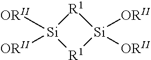
[0018] Although certain embodiments and examples are disclosed below, it will be understood by those in the art that the invention extends beyond the specifically disclosed embodiments and/or uses of the invention and obvious modifications and equivalents thereof. Thus, it is intended that the scope of the invention disclosed should not be limited by the particular disclosed embodiments described below.
[0019] As used herein, the term "substrate" may refer to any underlying material or materials that may be used to form, or upon which, a device, a circuit, or a film may be formed. A substrate can include a bulk material, such as silicon (e.g., single-crystal silicon) and can include one or more layers overlying the bulk material. Further, the substrate can include various topologies, such as recesses, lines, and the like formed within or on at least a portion of a layer of the substrate.
[0020] As used herein, the term "cyclical deposition" may refer to the sequential introduction of precursors (reactants) into a reaction chamber to deposit a layer over a substrate and includes processing techniques such as atomic layer deposition and cyclical chemical vapor deposition.
[0021] As used herein, the term "atomic layer deposition" (ALD) may refer to a vapor deposition process in which deposition cycles, typically a plurality of consecutive deposition cycles, are conducted in a process chamber. Generally, during each cycle, a precursor is chemisorbed to a deposition surface (e.g., a substrate surface that can include a previously deposited material from a previous ALD cycle or other material), forming about a monolayer or sub-monolayer of material that does not readily react with additional precursor (i.e., a self-limiting reaction). Thereafter, in some cases, a reactant (e.g., another precursor or reaction gas) may subsequently be introduced into the process chamber for use in converting the chemisorbed precursor to the desired material on the deposition surface. The reactant can be capable of further reaction with the precursor. Further, purging steps can also be utilized during each cycle to remove excess precursor from the process chamber and/or remove excess reactant and/or reaction byproducts from the process chamber after conversion of the chemisorbed precursor. Further, the term atomic layer deposition, as used herein, is also meant to include processes designated by related terms, such as chemical vapor atomic layer deposition, atomic layer epitaxy (ALE), molecular beam epitaxy (MBE), gas source MBE, or organometallic MBE, and chemical beam epitaxy when performed with alternating pulses of precursor(s)/reactive gas(es), and purge (e.g., inert carrier) gas(es).
[0022] As used herein, the term "cyclical chemical vapor deposition" may refer to any process wherein a substrate is sequentially exposed to two or more volatile precursors, which react and/or decompose on a substrate to produce a desired deposition.
[0023] Exemplary embodiments of the disclosure relate to structures that include a layer comprising SiOC. As used herein, unless stated otherwise, SiOC is not intended to limit, restrict, or define the bonding or chemical state, for example, the oxidation state of any of Si, O, C, and/or any other element in the film. Further, in some embodiments, SiOC thin films may comprise one or more elements in addition to Si, O, and/or C, such as H or N. In some embodiments, the SiOC films may comprise Si--C bonds and/or Si--O bonds. In some embodiments, the SiOC films may comprise Si--C bonds and Si--O bonds and may not comprise Si--N bonds. In some embodiments, the SiOC films may comprise Si--H bonds in addition to Si--C and/or Si--O bonds. In some embodiments, the SiOC films may comprise more Si--O bonds than Si--C bonds, for example, a ratio of Si--O bonds to Si--C bonds may be from about 1:10 to about 10:1. In some embodiments, the SiOC may comprise from about 0% to about 50% carbon on an atomic basis. In some embodiments, the SiOC may comprise from about 0.1% to about 40%, from about 0.5% to about 30%, from about 1% to about 30%, or from about 5% to about 20% carbon on an atomic basis. In some embodiments, the SiOC films may comprise from about 0% to about 70% oxygen on an atomic basis. In some embodiments, the SiOC may comprise from about 10% to about 70%, from about 15% to about 50%, or from about 20% to about 40% oxygen on an atomic basis. In some embodiments, the SiOC films may comprise about 0% to about 50% silicon on an atomic basis. In some embodiments, the SiOC may comprise from about 10% to about 50%, from about 15% to about 40%, or from about 20% to about 35% silicon on an atomic basis. In some embodiments, the SiOC may comprise from about 0.1% to about 40%, from about 0.5% to about 30%, from about 1% to about 30%, or from about 5% to about 20% hydrogen on an atomic basis. In some embodiments, the SiOC films may not comprise nitrogen. In some other embodiments, the SiOC films may comprise from about 0% to about 40% nitrogen on an atomic basis (at %). In some cases, as described in more detail below, the layer comprising SiOC can be deposited conformally over features on a substrate and/or can be selectively deposited on one material relative to another material on a substrate surface.
[0024] Turning now to the figures, FIG. 1 illustrates a method 100 of forming a structure in accordance with at least one embodiment of the disclosure. Method 100 includes the steps of providing a substrate within a reaction chamber (step 102), selectively depositing a layer comprising silicon nitride (step 104), and depositing a layer comprising SiOC (step 108). Method 100 also includes an optional treatment step (step 106) that can be used to treat the silicon nitride deposited during step 104.
[0025] During step 102, a substrate is provided into a reaction chamber of a reactor. In accordance with examples of the disclosure, the reaction chamber can form part of an atomic layer deposition (ALD) reactor. Exemplary single wafer reactors, suitable for use with method 100, include reactors designed specifically to perform ALD processes, which are commercially available from ASM International NV (Almere, The Netherlands). Exemplary suitable batch ALD reactors are also commercially available from ASM International NV. Various steps of method 100 can be formed within a single reaction chamber or can be performed in multiple reactor chambers, such as reaction chambers of a cluster tool. Optionally, a reactor including the reaction chamber can be provided with a heater to activate the reactions by elevating the temperature of one or more of the substrate and/or the reactants/precursors.
[0026] During step 102, the substrate can be brought to a desired temperature and pressure for deposition of silicon nitride during step 104. By way of examples, a temperature (e.g., of a substrate or a substrate support) within a reaction chamber can be between about 100.degree. C. and about 500.degree. C. or about 200.degree. C. and about 400.degree. C. A pressure within the reaction chamber can be about 0.5 Torr to about 20 Torr or about 5 Torr to about 15 Torr.
[0027] In accordance with examples of the disclosure, the substrate provided during step 102 can include a surface comprising a first material and a second material, the first material comprising a metal and the second material comprising one or more of an oxide, a nitride, and an oxynitride. The metal can be or include tungsten; the oxide can be or include silicon oxide; the nitride can be or include silicon nitride and the oxynitride can be or include silicon oxynitride.
[0028] During step 104, the layer comprising silicon nitride is selectively deposited on the first material (e.g., metal) relative to the second material (e.g., one or more of an oxide, a nitride, and an oxynitride). An exemplary technique for selectively depositing silicon nitride on the first material relative to the second material includes a cyclical deposition process, such as an ALD process.
[0029] One ALD cycle may comprise exposing the substrate to a first reactant (also referred to herein as a precursor), removing any unreacted first reactant and reaction byproducts from the reaction space and exposing the substrate to a second reactant, followed by a second removal step. The first reactant may include, for example, a silicon halide or another silicon source. Exemplary silicon halides include silicon tetraiodide (SiI.sub.4), silicon tetrabromide (SiBr.sub.4), silicon tetrachloride (SiCl.sub.4), hexachlorodisilane (Si.sub.2Cl.sub.6), hexaiododisilane (Si.sub.2I.sub.6), octoiodotrisilane (Si.sub.3I.sub.8). The second reactant may comprise a nitrogen source, such as nitrogen gas, ammonia (NH.sub.3), hydrazine (N.sub.2H.sub.4) or an alkyl-hydrazine, wherein the alkyl-hydrazine may refer to a derivative of hydrazine which may comprise an alkyl functional group and may also comprise additional functional groups. Non-limiting example embodiments of an alkyl-hydrazine may comprise at least one of tertbutylhydrazine (C.sub.4H.sub.9N.sub.2H.sub.3), methylhydrazine (CH.sub.3NHNH.sub.2) or dimethylhydrazine ((CH.sub.3).sub.2N.sub.2NH.sub.2).
[0030] During the purge steps, precursors/reactants can be temporally separated by inert gases, such as argon (Ar) or nitrogen (N.sub.2), to prevent gas-phase reactions between reactants and enable self-saturating surface reactions. In some embodiments, however, the substrate may be moved to separately contact a first vapor phase reactant and a second vapor phase reactant. Because the reactions can self-saturate, strict temperature control of the substrates and precise dosage control of the precursors is not usually required. However, the substrate temperature is preferably such that an incident gas species does not condense into monolayers or multimonolayers nor thermally decompose on the surface. Surplus chemicals and reaction byproducts, if any, are removed from the substrate surface, such as by purging the reaction space or by moving the substrate, before the substrate is contacted with the next reactive chemical. Undesired gaseous molecules can be effectively expelled from a reaction space with the help of an inert purging gas. A vacuum pump may be used to assist in the purging.
[0031] In some embodiments, exposing the substrate to a silicon halide source may comprise pulsing the silicon precursor over the substrate for a time period of between about 0.5 seconds and about 30 seconds, or between about 0.5 seconds and about 10 seconds, or between about 0.5 seconds and about 5 seconds. In addition, during the pulsing of the silicon precursor source over the substrate, the flow rate of the silicon precursor (e.g., silicon halide) source may be less than 2000 sccm, or less than 1000 sccm, or less than 500 sccm, or less than 250 sccm or even less than 100 sccm.
[0032] In some embodiments, exposing the substrate to the nitrogen source may comprise pulsing the nitrogen source over the substrate for a time period of between about 0.5 seconds to about 30 seconds, or between about 0.5 seconds to about 10 seconds, or between about 0.5 seconds to about 5 seconds. During the pulsing of the nitrogen source over the substrate, the flow rate of the nitrogen source may be less than 4000 sccm, or less than 2000 sccm, or less than 1000 sccm, or even less than 250 sccm.
[0033] The second vapor phase reactant comprising a nitrogen source may react with silicon-containing molecules left on the substrate surface. In some embodiments, the second phase nitrogen source may react with the silicon-containing molecules left on the substrate surface to deposit a silicon nitride film.
[0034] During the purge steps, excess reactant(s) and reaction byproducts, if any, may be removed from the substrate surface, for example, by a purging gas pulse and/or vacuum generated by a pumping system. Purging gas is preferably any inert gas, such as, without limitation, argon (Ar), nitrogen (N.sub.2) or helium (He). A phase is generally considered to immediately follow another phase if a purge (i.e., purging gas pulse) or other reactant removal step intervenes.
[0035] The cyclical deposition process for forming a silicon nitride film may be repeated one or more times until the desired thickness of the silicon nitride is achieved. For example, the cyclical deposition process comprises forming the silicon nitride film with a thickness of between approximately 0.3 nm and approximately 30 nm.
[0036] Once an initial desired thickness of the silicon nitride film is deposited, the silicon nitride film may be exposed to a plasma (step 106) in order to improve the material characteristics of the deposited silicon nitride film, i.e., such as improving the wet etch rate of the silicon nitride film. The same reaction chamber or separate reaction chambers can be utilized for deposition silicon nitride film and a step of exposing the layer comprising silicon nitride to a plasma treatment. In embodiments where different reaction chambers are utilized for the cyclical deposition process and the plasma treatment process, the substrate may be transferred from a first reaction chamber (for the silicon nitride film deposition) to a second reaction chamber (for the plasma treatment) without exposure to the ambient atmosphere. In other words, methods of the disclosure may comprise forming the silicon nitride film on the substrate by a cyclical deposition process and exposing the silicon nitride film to a plasma utilizing the same semiconductor processing apparatus. The semiconductor processing apparatus utilized for the cyclical deposition and the plasma treatment may comprise a cluster tool which comprises two or more reaction chambers and which may further comprise a transfer chamber through which the substrate may be transported between the first reaction chamber and the second reaction chamber. In some embodiments, the environment within the transfer chamber may control, i.e., the temperature, pressure and ambient gas, such that the substrate and particularly the silicon nitride are not exposed to the ambient atmosphere. In some embodiments, the reaction chamber configured for exposing the silicon nitride film to a plasma may be configured with a capacitively coupled plasma (CCP) source, an inductively coupled plasma (ICP) source or a remote plasma (RP) source.
[0037] During step 106, a source gas from which the plasma is generated may comprise one or more of nitrogen (N.sub.2), helium (He), hydrogen (H.sub.2) and argon (Ar). In particular embodiments of the disclosure, the source gas from which the plasma is generated may comprise a mixture of helium (He) and nitrogen (N.sub.2) and the proportion of helium (He) gas to nitrogen (N.sub.2) gas may be equal, i.e., 50% helium gas (He) to 50% nitrogen gas (N.sub.2) (e.g., about 50:50). In alternate embodiments, the proportion of helium (He) gas to nitrogen (N.sub.2) may be 10%:90%, or 20%:80%, or 30%:70%, or 40%:60%, or 60%:40%, or 70%:30%, or 80%:20%, or even 90%:10%.
[0038] In some embodiments of the disclosure, exposing the layer comprising silicon nitride to a plasma treatment may comprise applying a power to the plasma source gas(es) of greater than approximately 150 W, or greater than 300 W, or greater than 600 W, or even greater than 900 W. In addition, the reaction chamber for exposing the layer comprising silicon nitride to a plasma treatment may be operated at a reduced pressure, for example, in some embodiments, the reaction chamber for exposing the silicon nitride to a plasma may operate at a pressure of approximately less than 4 Torr, or may operate at a pressure of approximately less than 2 Torr, or may even operate at a pressure of approximately 1 Torr. In some embodiments, the substrate may be heated during the plasma treatment process, for example, exposing the silicon nitride film to a plasma may comprise heating the substrate and the associated silicon nitride film to a temperature of greater than approximately 100.degree. C., or to a temperature of greater than approximately 200.degree. C., or even to a temperature of greater than approximately 250.degree. C.
[0039] In some embodiments of the disclosure, exposing the silicon nitride film to a plasma comprises exposing the silicon nitride to a plasma for a time period of less than approximately 300 seconds, or for a time period of less than 150 seconds or even for a time period of less than 90 seconds. In certain embodiments of the disclosure, the silicon nitride may be exposed to the plasma treatment for a longer period of time, for example, for a time period greater than 2 minutes, or greater than 5 minutes, or even greater than 10 minutes. It should be noted that the longer silicon nitride film is exposed to the plasma, the more likely that the beneficial effects of the plasma treatment are to saturate, and very long plasma exposure times may result in damage to the silicon nitride film.
[0040] As a non-limiting example embodiment of the disclosure, exposing the silicon nitride film to a plasma may comprise a helium (He) and nitrogen (N.sub.2) (e.g., about 50%:50%) gas plasma in a reaction chamber comprising a capacitively coupled plasma (CCP) source with a plasma power of 600 W, and a reaction chamber pressure of 2 Torr for a time period of 90 seconds.
[0041] The plasma treatment may be performed after each silicon nitride deposition cycle or after a predetermined--e.g., two or more--deposition cycles. The deposition cycles and plasma treatment steps can be repeated a desired number of times until a desired thickness of the silicon nitride is obtained. Further, it may be appreciated that embodiments of the disclosure may also include methods wherein the substrate is first exposed to a plasma treatment step 106 prior to selectively depositing silicon nitride, step 104. It should also be appreciated that a number of plasma treatments may be performed in a single complete deposition cycle, as a well as a number of cyclical deposition cycles may be performed prior to plasma treatment.
[0042] After selectively depositing a layer comprising silicon nitride step 104 and optional step 106 are complete, a layer comprising SiOC is deposited overlying the layer comprising silicon nitride during step 108. The layer comprising SiOC can be deposited using cyclic deposition, such as cyclic CVD, ALD, or a hybrid CVD-ALD process. Further, such processes can be driven thermally and/or be plasma-enhanced. Step 108 may be performed in the same or different reaction chamber used during step 104. A pressure within the reaction chamber during this step can be about 0.5 to about 15 Torr or about 1 to about 10 Torr.
[0043] In accordance with exemplary embodiments of the disclosure, step 108 includes a PEALD process, wherein at least one deposition cycle of the PEALD process includes contacting a surface of the substrate with a vapor phase silicon precursor; contacting the adsorbed silicon species with at least one reactive species generated by plasma formed from a second reactant comprising hydrogen; and optionally repeating the contacting steps until a SiOC film of a desired thickness has been formed.
[0044] In some embodiments, thin SiOC films are formed by repetition of a self-limiting ALD cycle. In some embodiments, for forming SiOC films, each ALD cycle comprises at least two distinct phases. The contacting and removal of a reactant or precursor from the substrate may be considered a phase. In a first phase, a vapor phase first reactant or precursor comprising silicon contacts the substrate and forms no more than about one monolayer on the substrate surface. This reactant is also referred to herein as "the silicon precursor," "silicon-containing precursor," or "silicon reactant" and may be, for example, bis(triethoxysilyl)ethane (BTESE) or 3-methoxypropyltrimethoxysilane (MPTMS). In some embodiments, excess first vapor phase reactant and any reaction byproducts are removed from the proximity of the substrate surface. The first vapor phase reactant and any reaction byproducts may be removed from proximity with the substrate surface with the aid of a purge gas and/or vacuum. Excess reactant and/or reactant byproducts can be purged as described herein.
[0045] In a second phase, a second reactant comprising a reactive species contacts the substrate and may convert adsorbed silicon species to SiOC. In some embodiments, the second reactant comprises a hydrogen precursor. In some embodiments, the reactive species comprises an excited species. In some embodiments, the second reactant comprises a species from a hydrogen containing plasma. In some embodiments, the second reactant comprises hydrogen radicals, hydrogen atoms and/or hydrogen plasma. The second reactant may comprise other species that are not hydrogen precursors. In some embodiments, the second reactant may comprise a species from a noble gas, such as one or more of He, Ne, Ar, Kr, or Xe, for example, as radicals, in plasma form, or in elemental form. These reactive species from noble gases do not necessarily contribute material to the deposited film, but can in, some circumstances, contribute to film growth as well as help in the formation and ignition of plasma. In some embodiments, the reactive species generated from noble gases may affect the amount or extent of any damage to the underlying substrate. A skilled artisan will be able to select a noble gas or gases suitable for a particular application. In some embodiments, a gas that is used to form a plasma may flow constantly throughout the deposition process but only be activated intermittently. In some embodiments, a gas that is used to form a plasma does not comprise oxygen. In some embodiments, the adsorbed silicon precursor is not contacted with a reactive species generated by a plasma from oxygen. In some embodiments, a second reactant comprising reactive species is generated in a gas that does not comprise oxygen. For example, in some embodiments, a second reactant may comprise a plasma generated in a gas that does not comprise oxygen. In some embodiments, the second reactant may be generated in a gas comprising less than about 50 atomic % (at %) oxygen, less than about 30 at % oxygen, less than about 10 at % oxygen, less than about 5 at % oxygen, less than about 1 at % oxygen, less than about 0.1 at % oxygen, less than about 0.01 at % oxygen, or less than about 0.001 at % oxygen. As noted below, in other embodiments, the second reactant may include oxygen or another oxidant.
[0046] In some embodiments, a gas that is used to form a plasma does not comprise nitrogen. In some embodiments, the adsorbed silicon precursor is not contacted with a reactive species generated by a plasma from nitrogen. In some embodiments, a second reactant comprising reactive species is generated in a gas that does not comprise nitrogen. For example, in some embodiments, a second reactant may comprise a plasma generated in a gas that does not comprise nitrogen. However, in some embodiments, a gas that is used to form a plasma may comprise nitrogen. In some other embodiments, the second reactant may comprise nitrogen radicals, nitrogen atoms and/or nitrogen plasma. In some embodiments, the second reactant may be generated in a gas comprising less than about 25 atomic % (at %) nitrogen, less than about 20 at % nitrogen, less than about 15 at % nitrogen, less than about 10 at % nitrogen, less than about 5 at % nitrogen, less than about 1 at % nitrogen, less than about 0.1 at % nitrogen, less than about 0.01 at % nitrogen, or less than about 0.001 at % nitrogen. In some embodiments, the second reactant may be generated in a gas comprising hydrogen and nitrogen, for example, the second reactant may comprise H.sub.2 and N.sub.2. In some embodiments, the second reactant may be generated in a gas having a ratio of N.sub.2 to H.sub.2 (N.sub.2/H.sub.2) of (e.g., greater than zero and) less than about 20%, less than about 10%, or less than about 5%.
[0047] In some embodiments, a gas that is used to form a plasma does not comprise nitrogen or oxygen. In some embodiments, the adsorbed silicon precursor is not contacted with a reactive species generated by a plasma from nitrogen or oxygen. In some embodiments, a second reactant comprising reactive species is generated in a gas that does not comprise nitrogen or oxygen. For example, in some embodiments, a second reactant may comprise a plasma generated in a gas that does not comprise nitrogen or oxygen. In other cases, the second reactant may include oxygen and/or nitrogen. Excess second reactant and any reaction byproducts can be purged as described herein.
[0048] Additional phases may be added and phases may be removed as desired to adjust the composition of the final film. Further, one or more of the reactants may be provided with the aid of a carrier gas, such as Ar or He. In some embodiments, the silicon precursor and the second reactant are provided with the aid of a carrier gas.
[0049] In some embodiments, two of the phases may overlap, or be combined. For example, the silicon precursor and the second reactant may contact the substrate simultaneously in phases that partially or completely overlap. In addition, although referred to as the first and second phases, an the first and second reactants, the order of the phases may be varied, and an ALD cycle may begin with any one of the phases. That is, unless specified otherwise, the reactants can contact the substrate in any order, and the process may begin with any of the reactants.
[0050] As discussed in more detail below, in some embodiments for depositing a SiOC film, one or more deposition cycles begin by contacting the substrate with the silicon precursor, followed by the second precursor. In other embodiments, deposition may begin by contacting the substrate with the second precursor, followed by the silicon precursor.
[0051] In some embodiments, if desired, the exposed surfaces of the workpiece can be pretreated to provide reactive sites to react with the first phase of the ALD process. In some embodiments the substrate is pretreated (e.g., with a plasma) to provide a desired surface termination.
[0052] A gas can be provided to the reaction chamber continuously during each deposition cycle, or during the entire ALD process, and reactive species can be provided by generating a plasma in the gas, either in the reaction chamber or upstream of the reaction chamber. In some embodiments the gas does not comprise nitrogen. In some embodiments the gas may comprise noble gas, such as helium or argon. In some embodiments the gas is helium. In some embodiments the gas is argon. The flowing gas may also serve as a purge gas for the first and/or second reactant (or reactive species). For example, flowing argon may serve as a purge gas for a first silicon precursor and also serve as a second reactant (as a source of reactive species). In some embodiments, argon or helium may serve as a purge gas for a first precursor and a source of excited species for converting the silicon precursor to the SiOC film. In some embodiments the gas in which the plasma is generated does not comprise nitrogen and the adsorbed silicon precursor is not contacted with a reactive species generated by a plasma from nitrogen. In some embodiments the gas in which the plasma is generated does not comprise oxygen and the adsorbed silicon precursor is not contacted with a reactive species generated by a plasma from oxygen. In some embodiments the gas in which the plasma is generated does not comprise oxygen or nitrogen and the adsorbed silicon precursor is not contacted with a reactive species generated by a plasma from oxygen or nitrogen. In other cases, the plasma may contain nitrogen and/or oxygen.
[0053] The deposition cycles can be repeated until a film of the desired thickness and/or composition is obtained. In some embodiments the deposition parameters, such as the precursor flow rate, contacting time, removal time, and/or reactants themselves, may be varied in one or more deposition cycles during the ALD process in order to obtain a film with the desired characteristics.
[0054] In some embodiments, the substrate is contacted with the silicon reactant first. After an initial surface termination, if necessary or desired, the substrate is contacted with a first silicon reactant. In some embodiments a first silicon reactant pulse is supplied to the workpiece. In accordance with some embodiments, the first reactant pulse comprises a carrier gas flow and a volatile silicon species, such as BTESE or MPTMS, that is reactive with the workpiece surfaces of interest. Accordingly, the silicon reactant adsorbs upon these workpiece surfaces. The first reactant pulse self-saturates the workpiece surfaces with silicon reactant species such that any excess constituents of the first reactant pulse do not further react with the molecular layer formed by this process.
[0055] The first silicon reactant pulse can be supplied in gaseous form. The silicon precursor gas is considered "volatile" for purposes of the present description if the species exhibits sufficient vapor pressure under the process conditions to transport the species to the workpiece in sufficient concentration to saturate exposed surfaces.
[0056] In some embodiments the silicon reactant contacts the surface from about 0.05 seconds to about 5.0 seconds, about 0.1 seconds to about 3 seconds or about 0.2 seconds to about 1 second. The optimum contacting time can be readily determined by the skilled artisan based on the particular circumstances.
[0057] After sufficient time for about a molecular layer to adsorb on the substrate surface, excess first silicon reactant, and reaction byproducts, if any, are removed from the substrate surface. In some embodiments, removing excess reactant and reaction byproducts, if any, may comprise purging the reaction chamber. In some embodiments, the reaction chamber may be purged by stopping the flow of the first reactant while continuing to flow a carrier gas or purge gas for a sufficient time to diffuse or purge excess reactants and reactant by-products, if any, from the reaction space. In some embodiments, the excess first precursor is purged with the aid of inert gas, such as helium or argon, which is flowing throughout the ALD cycle. In some embodiments, the substrate may be moved from the reaction space containing the first reactant to a second, different reaction space. In some embodiments, the first reactant is removed for about 0.1 seconds to about 10 seconds, about 0.3 seconds to about 5 seconds, or about 0.3 seconds to about 1 second. Contacting and removal of the silicon reactant can be considered the first or silicon phase of the ALD cycle.
[0058] In the second phase, a second reactant comprising a reactive species, such as hydrogen plasma, is provided to the workpiece. Hydrogen plasma may be formed by generating a plasma in hydrogen in the reaction chamber or upstream of the reaction chamber, for example, by flowing the hydrogen (H.sub.2) through a remote plasma generator.
[0059] In some embodiments, plasma is generated in flowing H.sub.2 gas. In some embodiments, H.sub.2 is provided to the reaction chamber before the plasma is ignited or hydrogen atoms or radicals are formed. In some embodiments, the H.sub.2 is provided to the reaction chamber continuously and hydrogen containing plasma, atoms or radicals is created or supplied when needed.
[0060] Typically, the second reactant, for example, comprising hydrogen plasma, contacts the substrate for about 0.1 seconds to about 10 seconds. In some embodiments, the second reactant, such as hydrogen containing plasma, contacts the substrate for about 0.1 seconds to about 10 seconds, 0.5 seconds to about 5 seconds or 0.5 seconds to about 2 seconds. However, depending on the reactor type, substrate type and its surface area, the second reactant contacting time may be even higher than about 10 seconds. In some embodiments, contacting times can be on the order of minutes. The optimum contacting time can be readily determined by the skilled artisan based on the particular circumstances.
[0061] In some embodiments, the second reactant is provided in two or more distinct pulses, without introducing another reactant in between any of the two or more pulses. For example, in some embodiments, a plasma, such as a hydrogen containing plasma, is provided in two or more sequential pulses, without introducing a Si-precursor in between the sequential pulses. In some embodiments, during provision of plasma, two or more sequential plasma pulses are generated by providing a plasma discharge for a first period of time, extinguishing the plasma discharge for a second period of time, for example, from about 0.1 seconds to about 10 seconds, from about 0.5 seconds to about 5 seconds, or from about 1 second to about 4 seconds, and exciting it again for a third period of time before introduction of another precursor or a removal step, such as before the Si-precursor or a purge step. Additional pulses of plasma can be introduced in the same way. In some embodiments, a plasma is ignited for an equivalent period of time in each of the pulses.
[0062] In some embodiments, plasma, for example, hydrogen containing plasma, may be generated by applying RF power of from about 5 W to about 5000 W, from about 10 W to about 2000 W, from about 50 W to about 1000 W, or from about 200 W to about 800 W. In some embodiments, the RF power density may be from about 0.02 W/cm.sup.2 to about 2.0 W/cm.sup.2, or from about 0.05 W/cm.sup.2 to about 1.5 W/cm.sup.2. The RF power may be applied to a second reactant that flows during the plasma contacting time, that flows continuously through the reaction chamber, and/or that flows through a remote plasma generator. Thus, in some embodiments, the plasma is generated in situ, while in other embodiments, the plasma is generated remotely. In some embodiments, a showerhead reactor is utilized and plasma is generated between a susceptor (on top of which the substrate is located) and a showerhead plate. In some embodiments, the gap between the susceptor and showerhead plate is from about 0.1 cm to about 20 cm, from about 0.5 cm to about 5 cm, or from about 0.8 cm to about 3.0 cm.
[0063] After a time period sufficient to completely saturate and react the previously adsorbed molecular layer of silicon species with the plasma pulse, any excess reactant and reaction byproducts are removed from the substrate surface.
[0064] In some embodiments, removing excess reactant and reaction byproducts, if any, may comprise purging the reaction chamber. In some embodiments, the reaction chamber may be purged by stopping the flow of the second reactant while continuing to flow a carrier gas or purge gas for a sufficient time to diffuse or purge excess reactants and reactant by-products, if any, from the reaction space. In some embodiments, the excess second precursor is purged with the aid of inert gas, such as helium or argon, which is flowing throughout the ALD cycle. In some embodiments, the substrate may be moved from the reaction space containing the second reactant to a different reaction space. The removal may, in some embodiments, be from about 0.1 seconds to about 10 seconds, about 0.1 seconds to about 4 seconds, or about 0.1 seconds to about 0.5 seconds. Together, the reactive species contacting and removal represent a second, reactive species phase in a SiOC atomic layer deposition cycle.
[0065] The two phases together represent one ALD cycle, which is repeated to form SiOC thin films of a desired thickness. While the ALD cycle is generally referred to herein as beginning with the silicon phase, it is contemplated that in other embodiments, the cycle may begin with the reactive species phase. One of skill in the art will recognize that the first precursor phase generally reacts with the termination left by the last phase in the previous cycle. Thus, while no reactant may be previously adsorbed on the substrate surface or present in the reaction space, if the reactive species phase is the first phase in the first ALD cycle, in subsequent cycles, the reactive species phase will effectively follow the silicon phase. In some embodiments, one or more different ALD cycles are provided in the deposition process.
[0066] According to some embodiments of the present disclosure, PEALD reactions may be performed at temperatures ranging from about 25.degree. C. to about 700.degree. C., from about 50.degree. C. to about 600.degree. C., from about 100.degree. C. to about 450.degree. C., or from about 200.degree. C. to about 400.degree. C. In some embodiments, the optimum reactor temperature may be limited by the maximum allowed thermal budget. Therefore, in some embodiments, the reaction temperature is from about 100.degree. C. to about 300.degree. C. In some applications, the maximum temperature is around about 200.degree. C., and, therefore the PEALD process is run at or below that reaction temperature.
[0067] A number of different suitable Si precursors can be used in the presently disclosed PEALD processes. In some embodiments, the suitable Si precursors may not comprise nitrogen. In some embodiments, a suitable Si precursor may comprise a silane.
[0068] In some embodiments, a suitable Si precursor may comprise two Si atoms connected by, or bonded to, at least one hydrocarbon group. In some embodiments, a suitable Si precursor may comprise two Si atoms connected by, or bonded to, at least one alkyl group. In some embodiments, a suitable Si precursor may comprise two Si atoms connected by, or bonded to, at least one alkoxy group. In some embodiments, a suitable Si precursor may comprise two Si atoms connected by, or bonded to, at least one silyl group. In some embodiments, a suitable Si precursor may comprise two Si atoms connected by, or bonded to, at least one silyl ether group. In some embodiments, a suitable Si precursor may comprise at least one --SH group, wherein the --SH may be bonded to an alkyl chain or a silicon atom. In some embodiments, a suitable Si precursor may comprise at least one mercapto group. In some embodiments, a suitable Si precursor may comprise at least one --R--SH structure, wherein R may be a C.sub.1-C.sub.5 alkyl group. In some embodiments, a suitable Si precursor may comprise at least one --SH group on an alkyl chain and one or more alkoxy groups bonded to a silicon atom.
[0069] In some embodiments, a suitable Si precursor may comprise at least one Si atom attached or bonded to one or more alkoxy groups. In some embodiments, a suitable Si precursor may comprise at least one Si atom attached or bonded to one or more alkyl groups. In some embodiments, a suitable Si precursor may comprise at least one Si atom attached or bonded to at least an alkyl group and an alkoxy group.
[0070] In some embodiments, at least some Si precursors suitable for deposition of SiOC by PEALD processes may comprise bridged alkoxysilanes having the following general formula:
(R.sup.IIO).sub.3Si--R.sup.I--Si(OR.sup.II).sub.3 (1)
wherein each of R.sup.I and R.sup.II may be independently selected alkyl groups. In some embodiments, each of R.sup.I and R.sup.II are independently selected C.sub.1-C.sub.5 alkyl ligands, such as methyl, ethyl, n-propyl, isopropyl, tertbutyl, or pentyl.
[0071] According to some embodiments, some Si precursors may comprise bridged alkoxyalkylsilanes having the following general formula:
R.sup.III.sub.y(OR.sup.II).sub.xSi--R.sup.I--Si(OR.sup.II).sub.xR.sup.II- I.sub.y (2)
wherein each of R.sup.I, R.sup.II, and R.sup.III may be independently selected alkyl groups, and x+y=3. In some embodiments, each of R.sup.I and R.sup.II are independently selected C.sub.1-C.sub.5 alkyl ligands, such as methyl, ethyl, n-propyl, isopropyl, tertbutyl, or pentyl. In some embodiments, R.sup.III may be an independently selected C.sub.1-C.sub.8 alkyl ligand.
[0072] According to some embodiments, some Si precursors may comprise cyclic alkoxysilanes having the following general formula:
(R.sup.IIO).sub.2Si--R.sup.I.sub.2--Si(OR.sup.II).sub.2 (3)
[0073] Formula (3) may alternately be represented by the structural formula
##STR00001##
[0074] wherein each of R.sup.I and R.sup.II may be independently selected alkyl groups. In some embodiments, each of R.sup.I and R.sup.II are independently selected C.sub.1-C.sub.5 alkyl ligands, such as methyl, ethyl, n-propyl, isopropyl, tertbutyl, or pentyl.
[0075] According to some embodiments, some Si precursors may comprise cyclic alkoxyalkylsilanes having the following general formula:
R.sup.III.sub.y(OR.sup.II).sub.xSi--R.sup.I.sub.2--Si(OR.sup.II).sub.xR.- sup.III.sub.y (4)
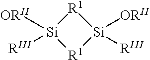
[0076] Formula (4) may alternately be represented by the structural formula
##STR00002##
wherein each of R.sup.I, R.sup.II, and R.sup.III may be independently selected alkyl groups, and x+y=2. In some embodiments, each of R.sup.I and R.sup.II are independently selected C.sub.1-C.sub.5 alkyl ligands, such as methyl, ethyl, n-propyl, isopropyl, tertbutyl, or pentyl. In some embodiments, R.sup.III may be an independently selected C.sub.1-C.sub.8 alkyl ligand.
[0077] According to some embodiments, some Si precursors may comprise linear alkoxysilanes having the following general formula:
(R.sup.IIO).sub.3Si--(O--Si--R.sup.I.sub.2).sub.n--O--Si(OR.sup.II).sub.- 3 (5)
wherein R.sup.I may be an independently selected alkyl group or hydrogen, R.sup.II may be an independently selected alkyl group, and n=1-4. In some embodiments, each of R.sup.I and R.sup.II are independently selected C.sub.1-C.sub.5 alkyl ligands, such as methyl, ethyl, n-propyl, isopropyl, tertbutyl, or pentyl. In some embodiments, R.sup.I may be hydrogen and R.sup.II may be an independently selected C.sub.1-C.sub.5 alkyl ligand.
[0078] According to some embodiments, some Si precursors may comprise linear alkoxysilanes having the following general formula:
R.sup.III.sub.y(OR.sup.II).sub.xSi--(--R.sup.I--Si).sub.n--Si(OR.sup.II)- .sub.xR.sup.III.sub.y (6)
wherein each of R.sup.I, R.sup.II, and R.sup.III may be independently selected alkyl groups, x+y=2, and n can be greater than or equal to 1. In some embodiments, R.sup.I and R.sup.II are independently selected C.sub.1-C.sub.5 alkyl ligands, such as methyl, ethyl, n-propyl, isopropyl, tertbutyl, or pentyl. In some embodiments, R.sup.III may be an independently selected C.sub.1-C.sub.8 alkyl ligand.
[0079] According to some embodiments, some Si precursors may comprise alkoxysilanes having the following general formula:
Si(OR.sup.I).sub.4 (7)
wherein R.sup.I may be an independently selected alkyl group. In some embodiments, R.sup.I may be an independently selected C.sub.1-C.sub.5 alkyl ligand, such as methyl, ethyl, n-propyl, isopropyl, tertbutyl, or pentyl.
[0080] According to some embodiments, some Si precursors may comprise alkoxyalkylsilanes having the following general formula:
Si(OR.sup.I).sub.4-xR.sup.II.sub.x (8)
wherein each of R.sup.I and R.sup.II may be independently selected alkyl groups, and x=1-3. In some embodiments, R.sup.I may be an independently selected C.sub.1-C.sub.5 alkyl ligand, such as methyl, ethyl, n-propyl, isopropyl, tertbutyl, or pentyl. In some embodiments, R.sup.II may be an independently selected C.sub.1-C.sub.8 alkyl ligand.
[0081] According to some embodiments, some Si precursors may comprise alkoxysilanes that do not comprise nitrogen and have the following general formula:
Si(OR.sup.I).sub.4-xR.sup.II.sub.x (9)
wherein R.sup.I may be an independently selected alkyl group, R.sup.II may be any ligand comprising carbon, hydrogen, and/or oxygen that does not comprise nitrogen, and x=1-3. In some embodiments, R.sup.I may be an independently selected C.sub.1-C.sub.5 alkyl ligand, such as methyl, ethyl, n-propyl, isopropyl, tertbutyl, or pentyl. In some embodiments, R.sup.II may comprise, for example, an alkenyl, alkynyl, phenyl, carbonyl, aldehyde, ester, ether, carboxyl, peroxy, hydroperoxy, thiol, acrylate, or methacrylate ligand.
[0082] According to some embodiments, some Si precursors may have the following general formula:
Si(OR.sup.I).sub.4-xR.sup.II.sub.x (10)
wherein x=0-3, R.sup.I may be an independently selected C.sub.1-C.sub.7 or C.sub.1-C.sub.5 alkyl ligand, and R.sup.II may be an independently selected ligand consisting of carbon, and/or hydrogen, and/or oxygen. For example, in some embodiments, R.sup.II can be an alkoxyalkyl group. In some embodiments, R.sup.II can be, for example, an alkenyl, alkynyl, phenyl, carbonyl, aldehyde, ester, ether, carboxyl, peroxy, or hydroperoxy group. In some embodiments, for example, R.sup.I is a methyl group, R.sup.II is a 3-methoxypropyl ligand, and x is 1.
[0083] According to some embodiments, some Si precursors may have the following general formula:
(R.sup.IO).sub.4-xSi--(R.sup.II--O--R.sup.III).sub.x (11)
wherein x=0-3, each of R.sup.I and R.sup.II may be an independently selected C.sub.1-C.sub.7 or C.sub.1-C.sub.5 alkyl ligand, and R.sup.III may be an independently selected ligand consisting of carbon, and/or hydrogen, and/or oxygen. For example, in some embodiments R.sup.III can be, for example, an alkenyl, alkynyl, phenyl, carbonyl, aldehyde, ester, ether, carboxyl, peroxy, or hydroperoxy group. In some embodiments, for example, R.sup.I, R.sup.II, and R.sup.III can each be a group independently selected from methyl, ethyl, i-propyl, n-propyl, n-butyl, i-butyl, and t-butyl.
[0084] According to some embodiments, some Si precursors may have the following general formula:
Si(R.sup.I).sub.4-xR.sup.II.sub.xR.sup.III.sub.y (12)
wherein x+y=0-4, R.sup.I is an alkoxide ligand having from 1 to 5 carbon atoms, or a halide, R.sup.II is any ligand comprising sulfur, and R.sup.III consists of one of a sulfhydryl, sulfide, disulfide, sulfinyl, sulfonyl, sulfino, sulfo, thiocyanate, isothiocyanate, or carbonothioyl functionality. In some embodiments, R.sup.I, R.sup.II, and R.sup.III may each be independently selected. In some embodiments, R.sup.I may comprise a methoxy ligand, R.sup.II may comprise 3-mercaptopropyl, x=1, and y=0. That is, in some embodiments, an Si precursor may comprise Si(OCH.sub.3).sub.3C.sub.3H.sub.6SH. In some embodiments, a Si precursor may comprise mercaptomethylmethyldiethoxysilane, 3-mercaptopropylmethyldimethoxysilane and/or 3-mercaptopropyltriethoxysilane.
[0085] In some embodiments, the silicon precursor does not comprise a halogen. In some embodiments, the silicon precursor does not comprise nitrogen. In some embodiments, the carbon chain may be unsaturated and contain double carbon-carbon bonds. In some other embodiments. the carbon chain may contain other atoms than carbon and hydrogen. According to some embodiments, suitable silicon precursors can include at least compounds having any of the general formulas (1) through (11). In some embodiments, the silicon precursor can comprise bis(triethoxysilyl)ethane (BTESE). In some embodiments, the silicon precursor can comprise 3-methoxypropyltrimethoxysilane (MPTMS or Si(OCH.sub.3).sub.3C.sub.3H.sub.6OCH.sub.3). In some embodiments, the silicon precursor can comprise (3-mercaptopropyl)trimethoxysilane.
[0086] In some embodiments, more than one silicon precursor may contact the substrate surface at the same time during an ALD phase. In some embodiments, the silicon precursor may comprise more than one of the silicon precursors described herein. In some embodiments, a first silicon precursor is used in a first ALD cycle and a second, different ALD precursor is used in a later ALD cycle. In some embodiments, multiple silicon precursors may be used during a single ALD phase, for example in order to optimize certain properties of the deposited SiOC film. In some embodiments, only one silicon precursor may contact the substrate during the deposition. In some embodiments, there may only be one silicon precursor and one second reactant or composition of second reactants in the deposition process. In some embodiments, there is no metal precursor in the deposition process. In some embodiments, the silicon precursor is not used as a silylating agent. In some embodiments, the deposition temperature and/or the duration of the silicon precursor contacting step are selected such that the silicon precursor does not decompose. In some embodiments, the silicon precursor may decompose during the silicon precursor contacting step. In some embodiments, the silicon precursor does not comprise a halogen, such as chlorine or fluorine.
[0087] As discussed above, the second reactant for depositing SiOC according to the present disclosure may comprise a hydrogen precursor, which may comprise a reactive species. In some embodiments, a reactive species includes, but is not limited to, radicals, plasmas, and/or excited atoms or species. Such reactive species may be generated by, for example, plasma discharge, hot-wire, or other suitable methods. In some embodiments, the reactive species may be generated remotely from the reaction chamber, for example, up-stream from the reaction chamber ("remote plasma"). In some embodiments, the reactive species may be generated in the reaction chamber, in the direct vicinity of the substrate, or directly above the substrate ("direct plasma").
[0088] Suitable plasma compositions of a PEALD process include hydrogen reactive species, that is, plasma, radicals of hydrogen, or atomic hydrogen in one form or another. In some embodiments, a second reactant may comprise a reactive species formed at least in part from H.sub.2. In some embodiments, a plasma may also contain noble gases, such as He, Ne, Ar, Kr and Xe, or Ar or He, in plasma form, as radicals, or in atomic form.
[0089] In some embodiments, the second reactant may comprise reactive species formed from H.sub.2. In some embodiments, the second reactant may be generated from a gas containing more than about 25 atomic % (at %) hydrogen, more than about 50 at % hydrogen, more than about 75 at % hydrogen, more than about 85 at % hydrogen, more than about 90 at % hydrogen, more than about 95 at % hydrogen, more than about 96 at %, 97 at %, 98 at %, or more than about 99 at % hydrogen.
[0090] In accordance with other embodiments of the disclosure, when the layer comprising SiOC comprises SiOCN, the second reactant can comprise nitrogen. For example, the second reactant can include nitrogen oxide (N.sub.2O) or ammonia (NH.sub.3). The SiOCN films can be deposited using thermal or plasma techniques. In the case of thermal deposition, a substrate temperature can be about 200 to about 700 C or about 300 to about 600 C and a pressure within the reaction chamber can be about 0.5 to about 40 or about 5 to about 25 Torr. Further, in accordance with various examples of these embodiments, oxygen and/or other oxidants can be used after second reactant pulse to reduce the carbon content in the layer comprising SiOCN. In some cases, only a silicon precursor can be used to deposit a layer comprising SiOCN. For example, (tetramethyl bis(2,2-dimethylhydrazino)disilane) can be used for thermal deposition of a layer comprising SiOCN without the need of another reactant.
[0091] In some embodiments, the gas used to generate reactive species, such as plasma, may consist essentially of hydrogen. Thus, in some embodiments, the second reactant may consist essentially of hydrogen plasma, radicals of hydrogen, or atomic hydrogen. In some embodiments, the second reactant may comprise more than about 25 at % hydrogen, more than about 50 at % hydrogen, more than about 75 at %, more than about 85 at %, more than about 90 at %, more than about 95 at %, more than about 96 at %, 97 at %, 98 at %, or more than about 99 at % hydrogen plasma, radicals of hydrogen, or atomic hydrogen. In some embodiments, the second reactant may be formed, at least in part, from H.sub.2 and one or more other gases, where the H.sub.2 and other gas or gases are provided at a flow ratio (Hz/other gas or gases), from about 1:1000 to about 1000:1 or greater. In some embodiments, the flow ratio (Hz/other gas or gases) may be greater than about 1:1000, greater than about 1:100, greater than about 1:50, greater than about 1:20, greater than about 1:10, greater than about 1:6, greater than about 1:3, greater than about 1:1, greater than about 3:1, greater than about 6:1, greater than about 10:1, greater than about 20:1, 50:1, 100:1, or 1000:1 or greater.
[0092] In some embodiments, the second reactant does not comprise any species generated from oxygen. Thus, in some embodiments, reactive species are not generated from a gas containing oxygen. In some embodiments, a second reactant comprising reactive species is generated from a gas that does not contain oxygen. For example, in some embodiments, a second reactant may comprise a plasma generated from a gas that does not contain oxygen. In some other embodiments, the second reactant may be generated from a gas containing less than about 50 atomic % (at %) oxygen, less than about 30 at % oxygen, less than about 10 at % oxygen, less than about 5 at % oxygen, less than about 1 at % oxygen, less than about 0.1 at % oxygen, less than about 0.01 at % oxygen, or less than about 0.001 at % oxygen. In some embodiments, a second reactant does not comprise O.sub.2, H.sub.2O or O.sub.3. In other embodiments, as described below, the second reactant includes an oxidant, such as N.sub.2O, as the second reactant.
[0093] In some embodiments, a hydrogen plasma may be free or substantially free of oxygen-containing species (e.g., oxygen ions, radicals, atomic oxygen). For example, oxygen-containing gas is not used to generate the hydrogen plasma. In some embodiments, oxygen-containing gas (e.g., O.sub.2 gas) is not flowed into the reaction chamber during the hydrogen plasma step.
[0094] In some embodiments, oxygen-containing gas is not used to generate the hydrogen plasma. In some embodiments, oxygen-containing gas (e.g., O.sub.2 gas) is not flowed into the reaction chamber during the hydrogen plasma step.
[0095] In some embodiments, the second reactant does not comprise any species generated from nitrogen. Thus, in some embodiments, reactive species are not generated from a gas containing nitrogen. In some embodiments, a second reactant comprising reactive species is generated from a gas that does not contain nitrogen. For example, in some embodiments, a second reactant may comprise a plasma generated from a gas that does not contain nitrogen. In some embodiments, the second reactant may be generated from a gas containing less than about 25 atomic % (at %) nitrogen, less than about 20 at % nitrogen, less than about 15 at % nitrogen, less than about 10 at % nitrogen, less than about 5 at % nitrogen, less than about 1 at % nitrogen, less than about 0.1 at % nitrogen, less than about 0.01 at % nitrogen, or less than about 0.001 at % nitrogen. In some embodiments, a second reactant does not comprise N.sub.2, NH.sub.3 or N.sub.2H.sub.4.
[0096] In some embodiments, a hydrogen plasma may be free or substantially free of nitrogen-containing species (e.g., nitrogen ions, radicals, atomic nitrogen). For example, nitrogen-containing gas is not used to generate the hydrogen plasma. In some embodiments, nitrogen-containing gas (e.g., N.sub.2 gas) is not flowed into the reaction chamber during the hydrogen plasma step.
[0097] However, in some other embodiments, nitrogen reactive species in the form of plasma, radicals of nitrogen, or atomic nitrogen in one form or another are also provided. Thus, in some embodiments, the second reactant may comprise reactive species formed from compounds having both N and H, such as NH.sub.3 and N.sub.2H.sub.4, a mixture of N.sub.2/H.sub.2 or other precursors having an N--H bond. In some embodiments, the second reactant may be formed, at least in part, from N.sub.2. In some embodiments, the second reactant may be formed, at least in part, from H.sub.2 and N.sub.2, where the H.sub.2 and N.sub.2 are provided at a flow ratio (H.sub.2/N.sub.2), from about 100:1 to about 1:100, from about 20:1 to about 1:20, from about 10:1 to about 1:10, from about 5:1 to about 1:5 and/or from about 2:1 to about 4:1, and in some cases 1:1. For example, a hydrogen-containing plasma for depositing SiOC can be generated using both N.sub.2 and H.sub.2 at one or more ratios described herein.
[0098] In some embodiments, the gas used to generate reactive species, such as plasma, may consist essentially of argon or another noble gas. In some embodiments, a plasma power used for generating a hydrogen-containing plasma can be about 5 Watts (W) to about 5000 W, about 10 W to about 2,000 W, about 50 W to about 1000 W, about 100 W to about 1000 W or about 100 W to about 500 W. In some embodiments, a plasma power used for generating a hydrogen-containing plasma can be about 100 W to about 300 W. In some embodiments, hydrogen containing plasma may also comprise argon or another noble gas.
[0099] In some cases, relatively high power and relatively high pressure can be used during film formation. For example, a power of about 400 W to about 800 W or 500 W to about 1000 W or about 700 W at a pressure of about 1 Torr to about 15 Torr or about 5 Torr to about 15 Torr or about 9 Torr can be used to increase conformality and step coverage of the layer comprising SiOC.
[0100] FIG. 2 illustrates a structure 200 in accordance with exemplary embodiments of the disclosure. Structure 200 includes a substrate 202 and a feature 203 formed thereon. Feature 203 includes a first conductive element 204, a second conductive element 206, a third element 208, a silicon nitride film 210, and a layer comprising SiOC 212.
[0101] Substrate 202 can include any suitable material, include semiconductor material and materials typically used to form semiconductor devices. By way of example, substrate 202 can be or include silicon, other Group IV semiconductor material, a Group III-V semiconductor, and/or a Group II-VI semiconductor.
[0102] First conductive element 204 can include any suitable conductive material. By way of example, first conductive element 204 can be or include polysilicon.
[0103] Second conductive element 206 can similarly be or include any suitable conductive material. By way of example, second conductive element 206 can be or include a metal, such as tungsten or copper.
[0104] Third element 208 can be or include any suitable material. By way of example, third element 208 can be or include hard mask material, such as silicon nitride or Al.sub.2O.sub.3.
[0105] A combination of silicon nitride layer 210 and a layer comprising SiOC can be used to form a spacer. As noted above, the combination of silicon nitride and the layer comprising SiOC can provide desired selectivity of silicon nitride deposition as well as desired wet etch rates.
[0106] Turning now to FIG. 3, a method of forming a structure 300 is illustrated. Method 300 includes the steps of providing a substrate within a reaction chamber (step 302) and selectively depositing a layer comprising SiOC overlying the first material (step 304).
[0107] During step 302, the substrate can be brought to a desired temperature and pressure for deposition of silicon nitride during step 104. By way of examples, a temperature (e.g., of a substrate or a substrate support) within a reaction chamber can be between about 100.degree. C. and about 500.degree. C., or about 150.degree. C. and about 450.degree. C. A pressure within the reaction chamber can be about 1 to about 30 or about 5 to about 20 Torr.
[0108] The substrate can include a surface comprising a first material and a second material. The first material can include an oxide and the second material can comprise a nitride. Exemplary oxides include silicon oxide, Al.sub.2O.sub.3 (aluminum oxides). By way of example, a silicon oxide can include thermally-deposited silicon oxide. Exemplary nitrides include silicon nitride, AN (aluminum nitrides). By way of example, the silicon nitride can be formed using low pressure CVD deposition techniques.
[0109] Step 304 can be the same or similar to step 108 described above. For example, step 304 can include use of the precursors, temperatures, pressures, and treatment steps described above in connection with step 108 and method 100.
[0110] FIG. 4 illustrates a structure 400 formed in accordance with exemplary embodiments of the disclosure. Structure 400 includes a substrate 402, nitride (e.g., silicon nitride) features 404, 406, an oxide (e.g., silicon oxide) feature 408, and an SiOC cap 410 selectively formed on the oxide feature, relative to the nitride features. SiOC cap 410 can be used as an etch stop layer. In accordance with exemplary embodiments of the disclosure, a thickness of SiOC cap 410 can range from greater than 0 to about 100 .ANG., about 20 to about 75 .ANG., or about 10 to about 50 .ANG.. SiOC cap layer can be formed of a layer comprising SiOC as described herein. Further, SiOC cap 410 can be selectively deposited onto oxide feature 408, with a selectivity greater than about 75, 90, 95, or 99 percent.
[0111] The example embodiments of the disclosure described above do not limit the scope of the invention, since these embodiments are merely examples of the embodiments of the invention, which is defined by the appended claims and their legal equivalents. Any equivalent embodiments are intended to be within the scope of this invention. Indeed, various modifications of the disclosure, in addition to those shown and described herein, such as alternative useful combinations of the elements described, may become apparent to those skilled in the art from the description. Such modifications and embodiments are also intended to fall within the scope of the appended claims.
* * * * *


D00000
D00001
D00002
D00003
D00004
XML
uspto.report is an independent third-party trademark research tool that is not affiliated, endorsed, or sponsored by the United States Patent and Trademark Office (USPTO) or any other governmental organization. The information provided by uspto.report is based on publicly available data at the time of writing and is intended for informational purposes only.
While we strive to provide accurate and up-to-date information, we do not guarantee the accuracy, completeness, reliability, or suitability of the information displayed on this site. The use of this site is at your own risk. Any reliance you place on such information is therefore strictly at your own risk.
All official trademark data, including owner information, should be verified by visiting the official USPTO website at www.uspto.gov. This site is not intended to replace professional legal advice and should not be used as a substitute for consulting with a legal professional who is knowledgeable about trademark law.