Trench Semiconductor Device Layout Configurations
Dosev; Dosi ; et al.
U.S. patent application number 16/724862 was filed with the patent office on 2020-04-23 for trench semiconductor device layout configurations. This patent application is currently assigned to Polar Semiconductor, LLC. The applicant listed for this patent is Polar Semiconductor, LLC SANKEN ELECTRIC CO., LTD.. Invention is credited to Dosi Dosev, Shunsuke Fukunaga, Tatsuya Kamimura, Steven L. Kosier, Don Rankila, Peter West.
| Application Number | 20200127092 16/724862 |
| Document ID | / |
| Family ID | 56690023 |
| Filed Date | 2020-04-23 |


View All Diagrams
| United States Patent Application | 20200127092 |
| Kind Code | A1 |
| Dosev; Dosi ; et al. | April 23, 2020 |
TRENCH SEMICONDUCTOR DEVICE LAYOUT CONFIGURATIONS
Abstract
A trench semiconductor device includes a layer of semiconductor material, an exterior trench pattern formed in the layer of semiconductor material, and an interior trench pattern formed in the layer of semiconductor material, at least partially surrounded by the exterior trench pattern. The exterior trench pattern includes a plurality of exterior trench portions that are each lined with dielectric material and filled with conductive material, and the interior trench pattern includes a plurality of interior trench portions that are each lined with dielectric material and filled with conductive material.
| Inventors: | Dosev; Dosi; (Woodbury, MN) ; Rankila; Don; (Farmington, MN) ; Kamimura; Tatsuya; (St. Louis Park, MN) ; Fukunaga; Shunsuke; (Saitama, JP) ; Kosier; Steven L.; (Lakeville, MN) ; West; Peter; (Minneapolis, MN) | ||||||||||
| Applicant: |
|
||||||||||
|---|---|---|---|---|---|---|---|---|---|---|---|
| Assignee: | Polar Semiconductor, LLC Bloomington MN SANKEN ELECTRIC CO., LTD. Saitama |
||||||||||
| Family ID: | 56690023 | ||||||||||
| Appl. No.: | 16/724862 | ||||||||||
| Filed: | December 23, 2019 |
Related U.S. Patent Documents
| Application Number | Filing Date | Patent Number | ||
|---|---|---|---|---|
| 15900571 | Feb 20, 2018 | 10580861 | ||
| 16724862 | ||||
| 15051642 | Feb 23, 2016 | |||
| 15900571 | ||||
| 62119555 | Feb 23, 2015 | |||
| Current U.S. Class: | 1/1 |
| Current CPC Class: | H01L 29/0692 20130101; H01L 29/0696 20130101; H01L 29/0653 20130101; H01L 29/7811 20130101 |
| International Class: | H01L 29/06 20060101 H01L029/06; H01L 29/78 20060101 H01L029/78 |
Claims
1. A trench semiconductor device comprising: a layer of semiconductor material; an exterior trench pattern formed in the layer of semiconductor material, the exterior trench pattern comprising first and second parallel exterior trench portions that form first and third opposite sides of a first rectangle shape, and third and fourth parallel exterior trench portions connected to and perpendicular to the first and second parallel exterior trench portions that form second and fourth opposite sides of the first rectangle shape, each of the first, second, third and fourth exterior trench portions being lined with dielectric material and filled with conductive material; and a first interior trench pattern formed in the layer of semiconductor material, surrounded by the exterior trench pattern, the first interior trench pattern comprising first and second parallel interior trench portions that form first and third opposite sides of a second rectangle shape, and third and fourth parallel interior trench portions connected to and perpendicular to the first and second parallel interior trench portions that form second and fourth opposite sides of the second rectangle shape, each of the first, second, third and fourth interior trench portions being lined with dielectric material and filled with conductive material.
2. The trench semiconductor device of claim 1, wherein the first exterior trench portion is parallel to the first interior trench portion.
3. The trench semiconductor device of claim 1, further comprising a second interior trench pattern formed in the layer of semiconductor material, surrounded by the exterior trench pattern, wherein the second interior trench pattern comprising fifth and sixth parallel interior trench portions that form first and third opposite sides of a third rectangle shape, and seventh and eighth parallel interior trench portions connected to and perpendicular to the fifth and sixth parallel interior trench portions that form second and fourth opposite sides of the third rectangle shape, each of the fifth, sixth, seventh and eighth interior trench portions being lined with dielectric material and filled with conductive material.
4. The trench semiconductor device of claim 3, wherein the second interior trench pattern is parallel to the first interior trench pattern.
5. The trench semiconductor device of claim 3, wherein the first exterior trench portion is parallel to the fifth interior trench portion.
6. The trench semiconductor device of claim 3, wherein the first and second interior trench patterns are separated from each other by an interior gap distance of about 2.0 .mu.m.
7. The trench semiconductor device of claim 3, wherein the fifth, the sixth, the seventh and the eighth interior trench portions each have a trench width of about 1.4 .mu.m.
8. The trench semiconductor device of claim 7, wherein the first, the second, the third and the fourth interior trench portions each have a trench width of about 1.4 .mu.m.
9. The trench semiconductor device of claim 3, wherein the first interior trench portion and the fifth interior trench portion are spaced from the first exterior trench portion by a gap distance of about 2.0 .mu.m.
10. The trench semiconductor device of claim 3, further comprising a third interior trench pattern formed in the layer of semiconductor material, surrounded by the exterior trench pattern, wherein the third interior trench pattern comprising ninth and tenth parallel interior trench portions that form first and third opposite sides of a fourth rectangle shape, and eleventh and twelfth parallel interior trench portions connected to and perpendicular to the ninth and tenth parallel interior trench portions that form second and fourth opposite sides of the fourth rectangle shape, each of the ninth, tenth, eleventh and twelfth interior trench portions being lined with dielectric material and filled with conductive material.
11. The trench semiconductor device of claim 10, wherein the second interior trench pattern is parallel to the third interior trench pattern.
12. The trench semiconductor device of claim 10, wherein the first exterior trench portion is parallel to the ninth interior trench portion.
13. The trench semiconductor device of claim 10, wherein the first, second and third interior trench patterns are separated from each other by an interior gap distance of about 2.0 .mu.m.
14. The trench semiconductor device of claim 10, wherein the ninth, the tenth, the eleventh and the twelfth interior trench portions each have a trench width of about 1.4 .mu.m.
15. The trench semiconductor device of claim 14, wherein the fifth, the sixth, the seventh and the eighth interior trench portions each have a trench width of about 1.4 .mu.m.
16. The trench semiconductor device of claim 15, wherein the first, the second, the third and the fourth interior trench portions each have a trench width of about 1.4 .mu.m.
17. The trench semiconductor device of claim 1, wherein the first, the second, the third and the fourth interior trench portions each have a trench width of about 1.4 .mu.m.
18. The trench semiconductor device of claim 1, wherein the first interior trench portion is spaced from the first exterior trench portion by a gap distance of about 2.0 .mu.m.
19. The trench semiconductor device of claim 1, wherein the first and second parallel exterior trench portions that form the first and third opposite sides of the first rectangle shape form long sides of the first rectangle shape, and wherein the third and fourth parallel exterior trench portions that form the second and fourth opposite sides of the first rectangle shape form short sides of the first rectangle shape.
20. The trench semiconductor device of claim 19, wherein the first and second parallel interior trench portions that form the first and third opposite sides of the second rectangle shape form short sides of the second rectangle shape, and wherein the third and fourth parallel interior trench portions that form the second and fourth opposite sides of the second rectangle shape form short sides of the second rectangle shape.
Description
CROSS-REFERENCE TO RELATED APPLICATION(S)
[0001] This application is a divisional of U.S. application Ser. No. 15/900,571, filed Feb. 20, 2018 for "Trench Semiconductor Device Layout Configurations" by D. Dosev et al., which is a divisional of U.S. application Ser. No. 15/051,642, filed Feb. 23, 2016 for "Trench Semiconductor Device Layout Configurations" by D. Dosev et al., which claims the benefit of U.S. Provisional Application No. 62/119,555 filed Feb. 23, 2015 for "Trench Semiconductor Device Layout Configurations" by D. Dosev et al.
INCORPORATION BY REFERENCE
[0002] U.S. application Ser. No. 15/900,571, U.S. application Ser. No. 15/051,642 and U.S. Provisional Application No. 62/119,555 are hereby incorporated herein by reference in their entireties.
BACKGROUND
[0003] The present invention relates to geometric layouts of trench semiconductor devices.
[0004] In many semiconductor devices, such as modern power MOSFET devices, it is desirable for the device to provide a high breakdown voltage that prevents reverse biasing and avalanche breakdown of the diode barriers of the device. In these devices, application of a reverse bias voltage across a diode barrier creates a depletion region in which the voltage gradient present there causes acceleration of charge carriers and the formation of electron-hole pairs by collisions between the charge carriers and dopant atoms. The electron-hole pairs generally migrate to opposite sides of the depletion region; however, higher levels of reverse bias voltage create higher electric fields in the depletion region, which accelerate the electron-hole pairs to a degree that results in further collisions that form further electron-hole pairs. This multiplication of charge carriers can eventually result in conduction of current in the reverse direction across the diode barrier, which is the condition known as avalanche breakdown of the device.
[0005] One technique that has been successfully employed to increase the breakdown voltage of a MOSFET device is to form the device as a trench semiconductor device. A trench semiconductor device consists of a plurality of parallel, interior MOS trenches formed in a semiconductor layer, with each trench being lined with dielectric material and then filled with a conductive material such as metal or doped polysilicon. In addition, an exterior trench is formed around an outside region of the device, having at least a portion generally perpendicular to the interior trenches. The gaps between the trenches effectively terminate the electric fields that tend to converge at the edges of the conductive legs formed in each trench, which results in a higher breakdown voltage. U.S. Pat. No. 6,683,363 illustrates an example of a trench semiconductor device.
[0006] Further developments in the geometry of a trench semiconductor device can provide characteristics and results that advance the state of the art, such as in terms of performance, cost, space efficiency, or others, or to simply provide an alternative configuration that may be appropriate for selected applications.
SUMMARY
[0007] A trench semiconductor device includes a layer of semiconductor material, an exterior trench pattern formed in the layer of semiconductor material, and an interior trench pattern formed in the layer of semiconductor material, at least partially surrounded by the exterior trench pattern. The exterior trench pattern includes a plurality of exterior trench portions that are each lined with dielectric material and filled with conductive material, and the interior trench pattern including a plurality of interior trench portions that are each lined with dielectric material and filled with conductive material. Various embodiments of the trench semiconductor device with unique trench patterns are disclosed. The various trench patterns provide configurations and/or performance characteristics that may be suitable for particular applications of the devices.
BRIEF DESCRIPTION OF THE DRAWINGS
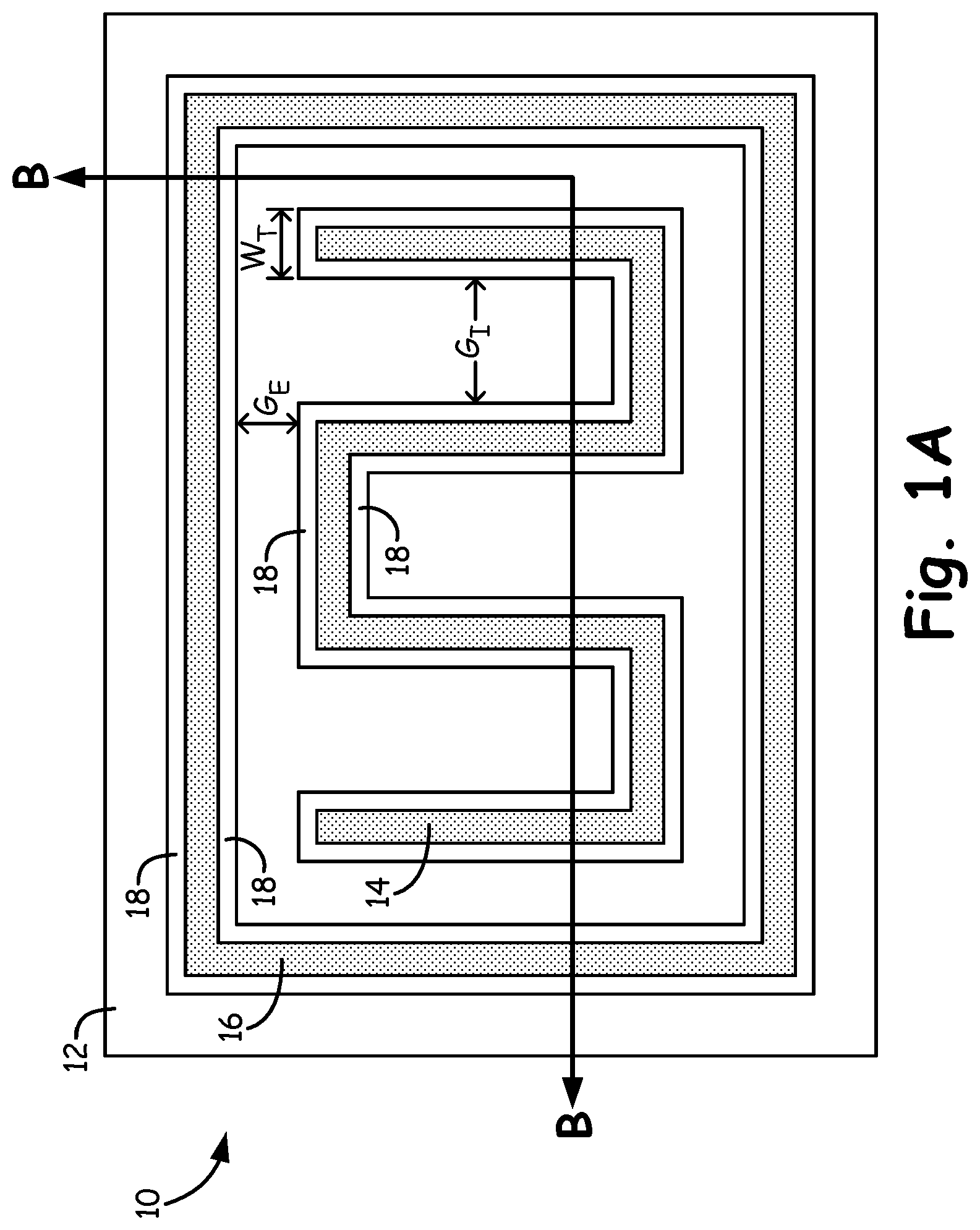
[0008] FIG. 1A is a top plan view of a MOSFET device formed as a trench semiconductor device according to an embodiment of the present invention.
[0009] FIG. 1B is a perspective view of the MOSFET device shown in FIG. 1A, sectioned at line B-B in FIG. 1A.
[0010] FIGS. 2-16 are top plan views of MOSFET devices formed as trench semiconductor devices according to various embodiments of the present invention.
[0011] FIG. 7A is a graph illustrating the measured breakdown voltages of a MOSFET device according to the embodiment of FIG. 7 for various dimensions of trench corner width and exterior trench gap length.
[0012] FIG. 8A is a graph illustrating the measured breakdown voltages of a MOSFET device according to the embodiment of FIG. 8 for various dimensions of gap distance and exterior trench length.
DETAILED DESCRIPTION
[0013] FIG. 1A is a top plan view of MOSFET device 10 formed as a trench semiconductor device according to an embodiment of the present invention. FIG. 1B is a perspective view of MOSFET device 10 sectioned at line B-B in FIG. 1A. As shown in FIGS. 1A and 1B, MOSFET device 10 includes semiconductor layer 12, a plurality of interior trenches 14 formed in semiconductor layer 12, and exterior trench 16 formed in semiconductor layer 12. Interior trenches 14 and exterior trench 16 are lined with dielectric material 18, such as silicon dioxide in some embodiments, and the dielectric lined trenches are filled with a conductive material (not shown) such as a metal or doped polysilicon. A metal layer (not shown) is formed over the entire structure, so that a metal/semiconductor barrier is formed where the metal layer adjoins the mesa regions of semiconductor layer 12 between interior trenches 14.
[0014] As best illustrated in FIG. 1A, interior trenches 14 are formed in a snake pattern enclosed by exterior trench 16. In the snake pattern, the legs of interior trenches 14 are separated from one another by interior gap distance G.sub.I. Each leg of interior trenches 14 has a trench width W.sub.T, and interior trenches 14 are spaced from exterior trench 16 by gap distance G.sub.E.
[0015] In an exemplary embodiment, gap distance G.sub.I may be about 2 micrometers (.mu.m), trench width W.sub.T may be about 1.4 .mu.m, and gap distance G.sub.E may be about 2 .mu.m.
[0016] FIGS. 2-16 are top plan views of MOSFET devices formed as trench semiconductor devices with alternative trench patterns. Only top plan views of these embodiments are shown, for simplicity, as the nature of the perspective view of each embodiment (similar to that shown in FIG. 1B) will be apparent to those skilled in the art based on the configuration illustrated in the corresponding top plan view. A fill pattern is used in FIGS. 2-16 to illustrate the trench patterns, for ease of understanding.
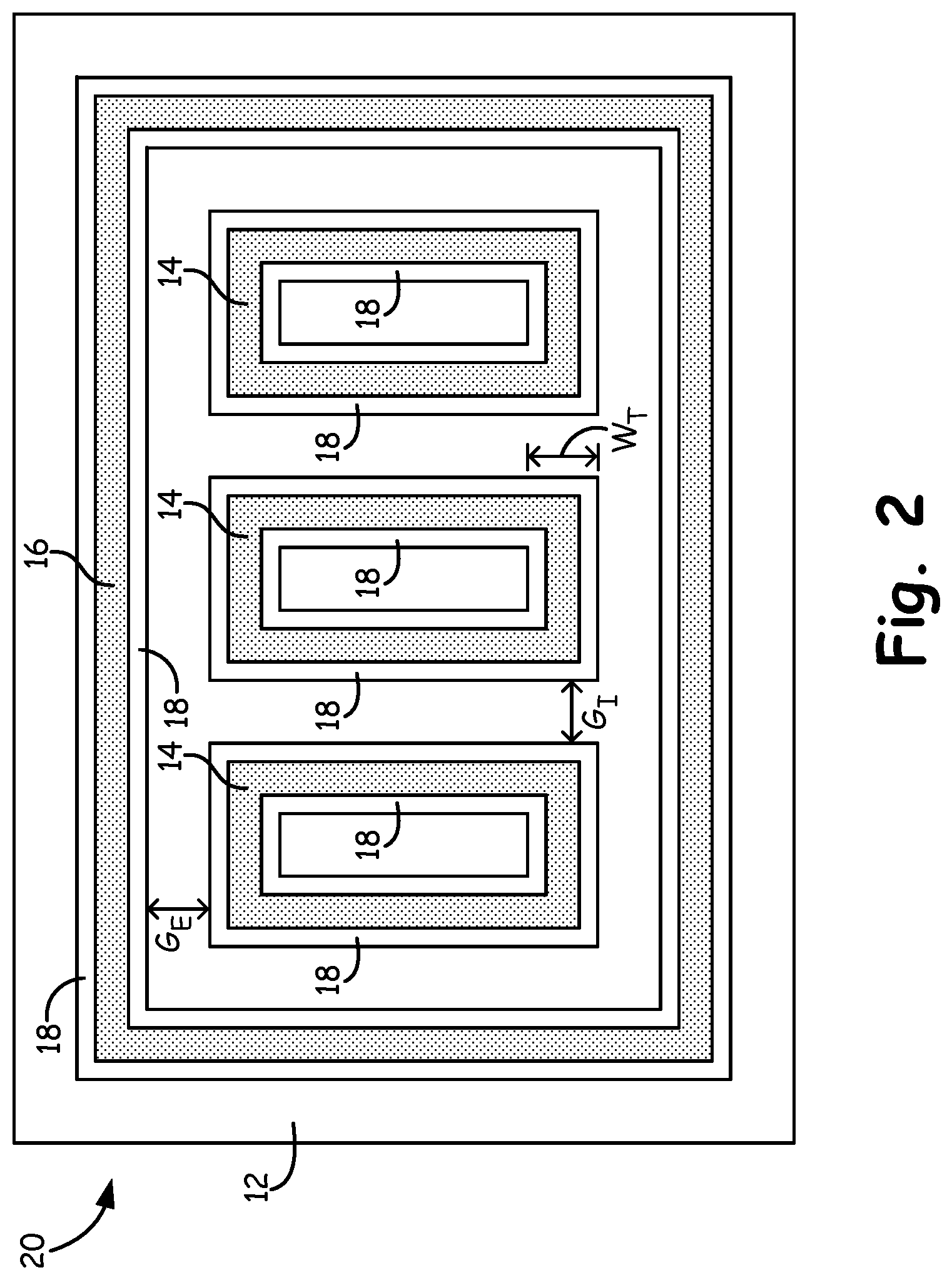
[0017] FIG. 2 is a top plan view of MOSFET device 20 formed as a trench semiconductor device according to another embodiment of the present invention. MOSFET device 20 includes semiconductor layer 12, a plurality of interior trenches 14 formed in semiconductor layer 12, and exterior trench 16 formed in semiconductor layer 12. Interior trenches 14 and exterior trench 16 are lined with dielectric material 18, such as silicon dioxide in some embodiments, and the dielectric lined trenches are filled with a conductive material (not shown) such as a metal or doped polysilicon. Interior trenches 14 are formed in a pattern of closed rectangles, enclosed by exterior trench 16. In the pattern shown, the sides of each closed rectangle formed by interior trenches 14 are separated from one another by interior gap distance G.sub.I. Each interior trench 14 has a trench width W.sub.T, and interior trenches 14 are spaced from exterior trench 16 by gap distance G.sub.E.
[0018] In an exemplary embodiment, gap distance G.sub.I may be about 2 .mu.m, trench width W.sub.T may be about 1.4 .mu.m, and gap distance G.sub.E may be about 2 .mu.m.
[0019] FIG. 3 is a top plan view of MOSFET device 30 formed as a trench semiconductor device according to another embodiment of the present invention. MOSFET device 30 includes semiconductor layer 12, a plurality of interior trenches 14 formed in semiconductor layer 12, intermediate trench 16a formed in semiconductor layer 12, and exterior trench 16b formed in semiconductor layer 12. Interior trenches 14, intermediate trench 16a and exterior trench 16b are lined with dielectric material 18, such as silicon dioxide in some embodiments, and the dielectric lined trenches are filled with a conductive material (not shown) such as a metal or doped polysilicon. Interior trenches 14 are formed in a snake pattern enclosed by intermediate trench 16a, and intermediate trench 16a is enclosed by exterior trench 16b. In the snake pattern, the legs of interior trenches 14 are separated from one another by interior gap distance G.sub.I. Each leg of interior trenches 14 has a trench width W.sub.T, and interior trenches 14 are spaced from intermediate trench 16a by gap distance G.sub.E. Intermediate trench 16a is separated from exterior trench 16b by gap distance G.sub.T.
[0020] In an exemplary embodiment, gap distance G.sub.I may be about 2 .mu.m, trench width W.sub.T may be about 1.4 .mu.m, gap distance G.sub.E may be about 2 .mu.m, and gap distance G.sub.T may be about 2 .mu.m.
[0021] FIG. 4 is a top plan view of MOSFET device 40 formed as a trench semiconductor device according to another embodiment of the present invention. MOSFET device 40 includes semiconductor layer 12, a plurality of interior trenches 14 formed in semiconductor layer 12, and segmented exterior trench 16 having gaps 42 therein formed in semiconductor layer 12. Interior trenches 14 and exterior trench 16 are lined with dielectric material 18, such as silicon dioxide in some embodiments, and the dielectric lined trenches are filled with a conductive material (not shown) such as a metal or doped polysilicon. Interior trenches 14 are formed in a snake pattern partially enclosed by segmented exterior trench 16. In the snake pattern, the legs of interior trenches 14 are separated from one another by interior gap distance G.sub.I. Each leg of interior trenches 14 has a trench width W.sub.T, and interior trenches 14 are spaced from exterior trench 16 by gap distance G.sub.E. Gaps 42 in segmented exterior trench 16 have a gap length G.sub.O.
[0022] In an exemplary embodiment, gap distance G.sub.I may be about 2 .mu.m, trench width W.sub.T may be about 1.4 .mu.m, gap distance G.sub.E may be about 2 .mu.m, and gap length G.sub.O may be about 2 .mu.m.
[0023] FIG. 5 is a top plan view of MOSFET device 50 formed as a trench semiconductor device according to another embodiment of the present invention. MOSFET device 50 includes semiconductor layer 12, a plurality of interior trenches 14 formed in semiconductor layer 12, and exterior trench 16 having notch features 52 formed in semiconductor layer 12. Interior trenches 14 and exterior trench 16 are lined with dielectric material 18, such as silicon dioxide in some embodiments, and the dielectric lined trenches are filled with a conductive material (not shown) such as a metal or doped polysilicon. Interior trenches 14 are formed in a snake pattern enclosed by exterior trench 16. In the snake pattern, the legs of interior trenches 14 are separated from one another by interior gap distance G.sub.I. Each leg of interior trenches 14 has a trench width W.sub.T, and interior trenches 14 are spaced from exterior trench 16 by gap distance G.sub.E. Notch features 52 in exterior trench 16 are formed adjacent to openings between the legs of the snake pattern of interior trench 14, and each notch feature has an extending width W.sub.N.
[0024] In an exemplary embodiment, gap distance G.sub.I may be about 2 .mu.m, trench width W.sub.T may be about 1.4 .mu.m, gap distance G.sub.E may be about 2 .mu.m, and extending width W.sub.N may be about 0.5 .mu.m.
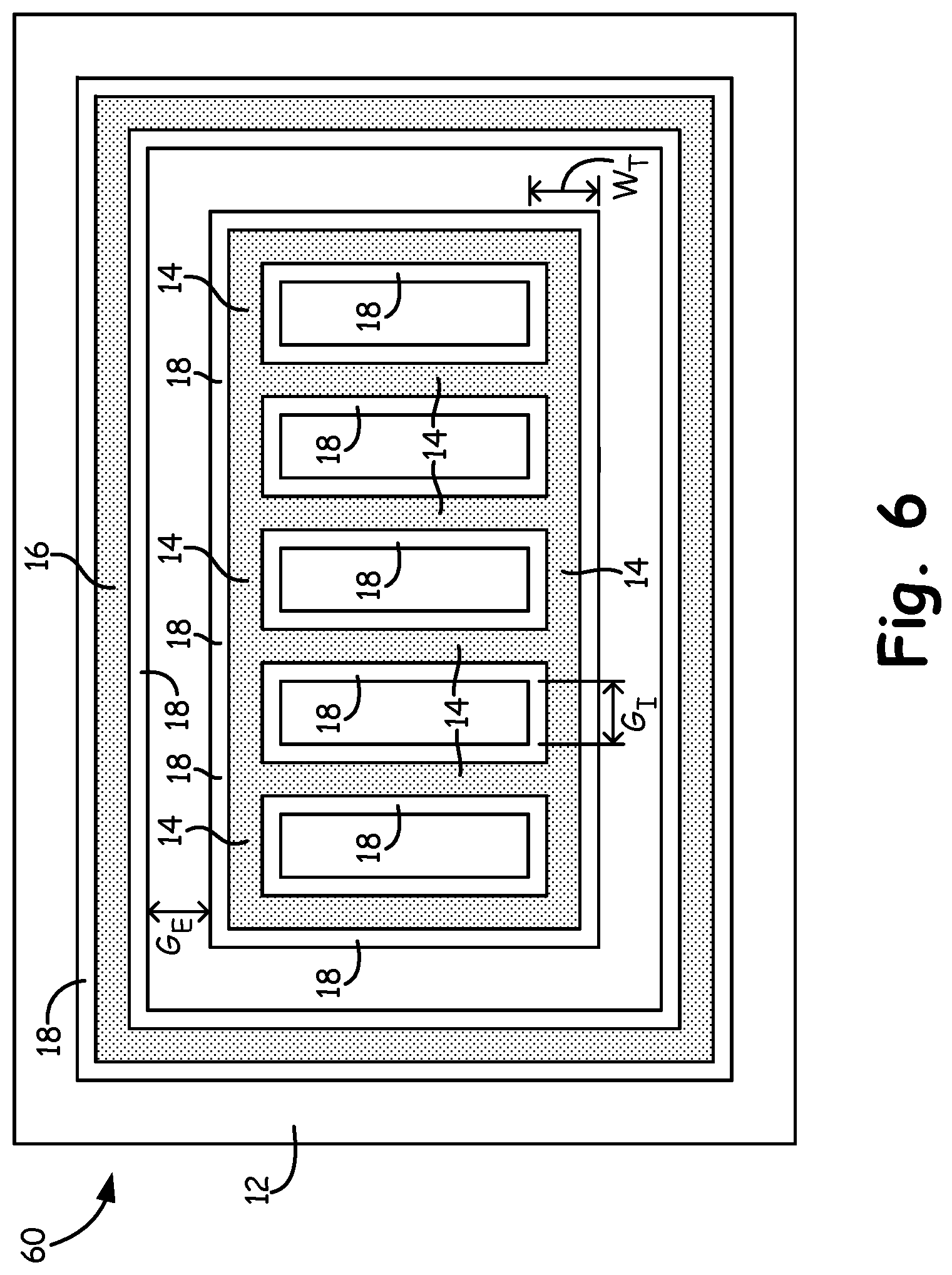
[0025] FIG. 6 is a top plan view of MOSFET device 60 formed as a trench semiconductor device according to another embodiment of the present invention. MOSFET device 60 includes semiconductor layer 12, a plurality of interior trenches 14 formed in semiconductor layer 12, and exterior trench 16 formed in semiconductor layer 12. Interior trenches 14 and exterior trench 16 are lined with dielectric material 18, such as silicon dioxide in some embodiments, and the dielectric lined trenches are filled with a conductive material (not shown) such as a metal or doped polysilicon. Interior trenches 14 are formed in a pattern having an outer frame and a plurality of vertical trench legs connecting the top and bottom horizontal segments of the outer frame. In the pattern shown, the vertical legs of interior trenches 14 are separated from one another by interior gap distance G.sub.I. Interior trenches 14 have a trench width W.sub.T, and interior trenches 14 are spaced from exterior trench 16 by gap distance G.sub.E.
[0026] In an exemplary embodiment, gap distance G.sub.I may be about 2 .mu.m, trench width W.sub.T may be about 1.4 .mu.m, and gap distance G.sub.E may be about 2 .mu.m.
[0027] FIG. 7 is a top plan view of MOSFET device 70 formed as a trench semiconductor device according to another embodiment of the present invention. MOSFET device 70 includes semiconductor layer 12, a plurality of interior trenches 14 formed in semiconductor layer 12, and segmented exterior trench 16 having gaps 72 therein formed in semiconductor layer 12. Interior trenches 14 and exterior trench 16 are lined with dielectric material 18, such as silicon dioxide in some embodiments, and the dielectric lined trenches are filled with a conductive material (not shown) such as a metal or doped polysilicon. Interior trenches 14 are formed in a pattern of vertical trench legs. In the pattern shown, the vertical legs of interior trenches 14 are separated from one another by interior gap distance G.sub.I. Interior trenches 14 have a trench width W.sub.T, and interior trenches 14 are spaced from exterior trench 16 by gap distance G.sub.E. Gaps 72 in segmented exterior trench 16 have a gap length G.sub.O.
[0028] In an exemplary embodiment, gap distance G.sub.I may be about 2 .mu.m, trench width W.sub.T may be about 1.4 .mu.m, gap distance G.sub.E may be about 2 .mu.m, gap length G.sub.O may be about 1.7 .mu.m, and trench corner width W.sub.C may be about 1.5 .mu.m. In other embodiments, these dimensions may be adjusted to control the breakdown voltage at the termination of MOSFET device 70. FIG. 7A is a graph illustrating the measured breakdown voltages of MOSFET device 70 for various dimensions of trench corner width W.sub.C and exterior trench gap length G.sub.O. As can be seen in FIG. 7A, the dimensions of trench corner width W.sub.C and exterior trench gap length G.sub.O affect the breakdown voltage of the device, and can be controlled in order to provide a desired breakdown voltage value.
[0029] Specific examples are shown in FIG. 7A, illustrating that a breakdown voltage of 117 Volts was achieved for an embodiment with exterior trench gap length G.sub.O of 0.7 .mu.m and a trench corner width W.sub.C of 2.5 .mu.m. A similar breakdown voltage of 117 Volts was also achieved for an embodiment with an exterior trench gap length G.sub.O of 1.0 .mu.m and a trench corner width W.sub.C of 2.2 .mu.m. A breakdown voltage of 118 Volts was achieved for an embodiment with an exterior trench gap length G.sub.O of 1.25 .mu.m and a trench corner width W.sub.C of 2.2 .mu.m. At an exterior trench gap length G.sub.O of 1.5 .mu.m, a breakdown voltage of 112 Volts was achieved for an embodiment with a trench corner width W.sub.C of 1.5 .mu.m, a breakdown voltage of 117 Volts was achieved for an embodiment with a trench corner width W.sub.C of 2.0 .mu.m, and a breakdown voltage of 118 Volts was achieved for an embodiment with a trench corner width W.sub.C of 2.2 .mu.m. A breakdown voltage of 121 Volts was achieved for an embodiment with an exterior trench gap length G.sub.O of 2.0 .mu.m and a trench corner width W.sub.C of 2.2 .mu.m.
[0030] FIG. 8 is a top plan view of MOSFET device 80 formed as a trench semiconductor device according to another embodiment of the present invention. MOSFET device 80 includes semiconductor layer 12, a plurality of interior trenches 14 formed in semiconductor layer 12, and segmented exterior trench 16 having gaps 82 therein formed in semiconductor layer 12. Interior trenches 14 and exterior trench 16 are lined with dielectric material 18, such as silicon dioxide in some embodiments, and the dielectric lined trenches are filled with a conductive material (not shown) such as a metal or doped polysilicon. Interior trenches 14 are formed in a pattern of vertical trench legs. In the pattern shown, the vertical legs of interior trenches 14 are separated from one another by interior gap distance G.sub.I. Interior trenches 14 have a trench width W.sub.T, and interior trenches 14 are spaced from exterior trench 16 by gap distance G.sub.E. Gaps 82 in segmented exterior trench 16 have a gap length G.sub.O. Exterior trench 16 is segmented in the embodiment shown in FIG. 8 so that the segments of exterior trench 16 line up with the legs of interior trench 14.
[0031] In an exemplary embodiment, gap distance G.sub.C may be about 2 .mu.m, trench width W.sub.T may be about 1.4 .mu.m, gap distance G.sub.E may be about 2 .mu.m, and exterior trench length L.sub.T may be about 2 .mu.m. In other embodiments, these dimensions may be adjusted to control the breakdown voltage at the termination of MOSFET device 80. FIG. 8A is a graph illustrating the measured breakdown voltages of MOSFET device 80 for various dimensions of gap distance G.sub.E and exterior trench length L.sub.T. As can be seen in FIG. 8A, the dimensions of gap distance G.sub.E and exterior trench length L.sub.T affect the breakdown voltage of the device, and can be controlled in order to provide a desired breakdown voltage value.
[0032] Specific examples are shown in FIG. 8A, illustrating that a breakdown voltage of 114 Volts was achieved for an embodiment with a gap distance G.sub.E of 1.0 .mu.m and an exterior trench length L.sub.T of 2.5 .mu.m. A similar breakdown voltage of 114 Volts was also achieved for an embodiment with a gap distance G.sub.E of 1.5 .mu.m and an exterior trench length L.sub.T of 2.5 .mu.m. At a gap distance G.sub.E of 2.0 .mu.m, a breakdown voltage of 109 Volts was achieved for an embodiment with an exterior trench length L.sub.T of 3.5 .mu.m, and a breakdown voltage of 111 Volts was achieved for an embodiment with an exterior trench length L.sub.T of 5.0 .mu.m. A breakdown voltage of 111 Volts was achieved for an embodiment with a gap distance G.sub.E of 2.5 .mu.m and exterior trench length L.sub.T of 2.5 .mu.m. A breakdown voltage of 112 Volts was achieved for an embodiment with a gap distance G.sub.E of 3.0 .mu.m and exterior trench length L.sub.T of 2.5 .mu.m, and also for an embodiment with a gap distance G.sub.E of 3.5 .mu.m and exterior trench length L.sub.T of 2.5 .mu.m.
[0033] FIG. 9 is a top plan view of MOSFET device 90 formed as a trench semiconductor device according to another embodiment of the present invention. MOSFET device 90 includes semiconductor layer 12, a plurality of interior trenches 14 formed in semiconductor layer 12, and exterior trench 16 formed in semiconductor layer 12. Interior trenches 14 and exterior trench 16 are lined with dielectric material 18, such as silicon dioxide in some embodiments, and the dielectric lined trenches are filled with a conductive material (not shown) such as a metal or doped polysilicon. Interior trenches 14 are formed in a snake pattern enclosed by exterior trench 16. The snake pattern is angled diagonally within exterior trench 16 as shown in FIG. 9. In the snake pattern, the legs of interior trenches 14 are separated from one another by interior gap distance G.sub.I. Each leg of interior trenches 14 has a trench width W.sub.T, and interior trenches 14 are spaced from exterior trench 16 by a minimum gap distance G.sub.E.
[0034] In an exemplary embodiment, gap distance G.sub.I may be about 2 .mu.m, trench width W.sub.T may be about 1.4 .mu.m, and gap distance G.sub.E may be about 2 .mu.m.
[0035] FIG. 10 is a top plan view of MOSFET device 100 formed as a trench semiconductor device according to another embodiment of the present invention. MOSFET device 100 includes semiconductor layer 12, a plurality of interior trenches 14 formed in semiconductor layer 12, and exterior trench 16 formed in semiconductor layer 12. Interior trenches 14 and exterior trench 16 are lined with dielectric material 18, such as silicon dioxide in some embodiments, and the dielectric lined trenches are filled with a conductive material (not shown) such as a metal or doped polysilicon. Interior trenches 14 are formed in a grid pattern enclosed by exterior trench 16. In the grid pattern, the legs of interior trenches 14 are separated from one another by interior gap distance G.sub.I. Each leg of interior trenches 14 has a trench width W.sub.T, and interior trenches 14 are spaced from exterior trench 16 by gap distance G.sub.E.
[0036] In an exemplary embodiment, gap distance G.sub.I may be about 4.5 .mu.m, trench width W.sub.T may be about 1.4 .mu.m, and gap distance G.sub.E may be about 2 .mu.m.
[0037] FIG. 11 is a top plan view of MOSFET device 110 formed as a trench semiconductor device according to another embodiment of the present invention. MOSFET device 110 includes semiconductor layer 12, a plurality of interior trenches 14 formed in semiconductor layer 12, and exterior trench 16 formed in semiconductor layer 12. Interior trenches 14 and exterior trench 16 are lined with dielectric material 18, such as silicon dioxide in some embodiments, and the dielectric lined trenches are filled with a conductive material (not shown) such as a metal or doped polysilicon. Interior trenches 14 are formed in a grid pattern enclosed by exterior trench 16. In the grid pattern, the legs of interior trenches 14 are separated from one another by interior gap distance G.sub.I. The vertical legs of interior trenches 14 extend beyond a square/rectangular grid pattern at vertical trench extensions 112. Each leg of interior trenches 14 has a trench width W.sub.T, and interior trenches 14 are spaced from exterior trench 16 by gap distance G.sub.E.
[0038] In an exemplary embodiment, gap distance G.sub.I may be about 4.5 .mu.m, trench width W.sub.T may be about 1.4 .mu.m, and gap distance G.sub.E may be about 2 .mu.m.
[0039] FIG. 12 is a top plan view of MOSFET device 120 formed as a trench semiconductor device according to another embodiment of the present invention. MOSFET device 120 includes semiconductor layer 12, a plurality of interior trenches 14 formed in semiconductor layer 12, and exterior trench 16 formed in semiconductor layer 12. Interior trenches 14 and exterior trench 16 are lined with dielectric material 18, such as silicon dioxide in some embodiments, and the dielectric lined trenches are filled with a conductive material (not shown) such as a metal or doped polysilicon. Interior trenches 14 are formed in a pattern of vertical trench legs. In the pattern shown, the vertical legs of interior trenches 14 are separated from one another by interior gap distance G.sub.I. Interior trenches 14 have a trench width W.sub.T, and interior trenches 14 are spaced from exterior trench 16 by gap distance G.sub.E. Exterior trench 16 has a trench width that is greater than the trench width W.sub.T of interior trenches 14, such as twice the trench width W.sub.T in an exemplary embodiment.
[0040] In an exemplary embodiment, gap distance G.sub.I may be about 2.0 .mu.m, trench width W.sub.T may be about 1.4 .mu.m, and gap distance G.sub.E may be about 2 .mu.m.
[0041] FIG. 13 is a top plan view of MOSFET device 130 formed as a trench semiconductor device according to another embodiment of the present invention. MOSFET device 130 includes semiconductor layer 12, a plurality of interior trenches 14 formed in semiconductor layer 12, and exterior trench 16 formed in semiconductor layer 12. Middle dividing trench 136 is also formed in semiconductor layer 12, dividing the interior region inside exterior trench 16 into two separate regions, each of which includes a plurality of interior trenches 14. Interior trenches 14, exterior trench 16 and middle dividing trench 136 are lined with dielectric material 18, such as silicon dioxide in some embodiments, and the dielectric lined trenches are filled with a conductive material (not shown) such as a metal or doped polysilicon. Interior trenches 14 are formed in a pattern of vertical trench legs. In the pattern shown, the vertical legs of interior trenches 14 are separated from one another by interior gap distance G.sub.I. Interior trenches 14 have a trench width W.sub.T, and interior trenches 14 are spaced from exterior trench 16 by gap distance G.sub.E.
[0042] In an exemplary embodiment, gap distance G.sub.I may be about 2.0 .mu.m, trench width W.sub.T may be about 1.4 .mu.m, and gap distance G.sub.E may be about 2 .mu.m.
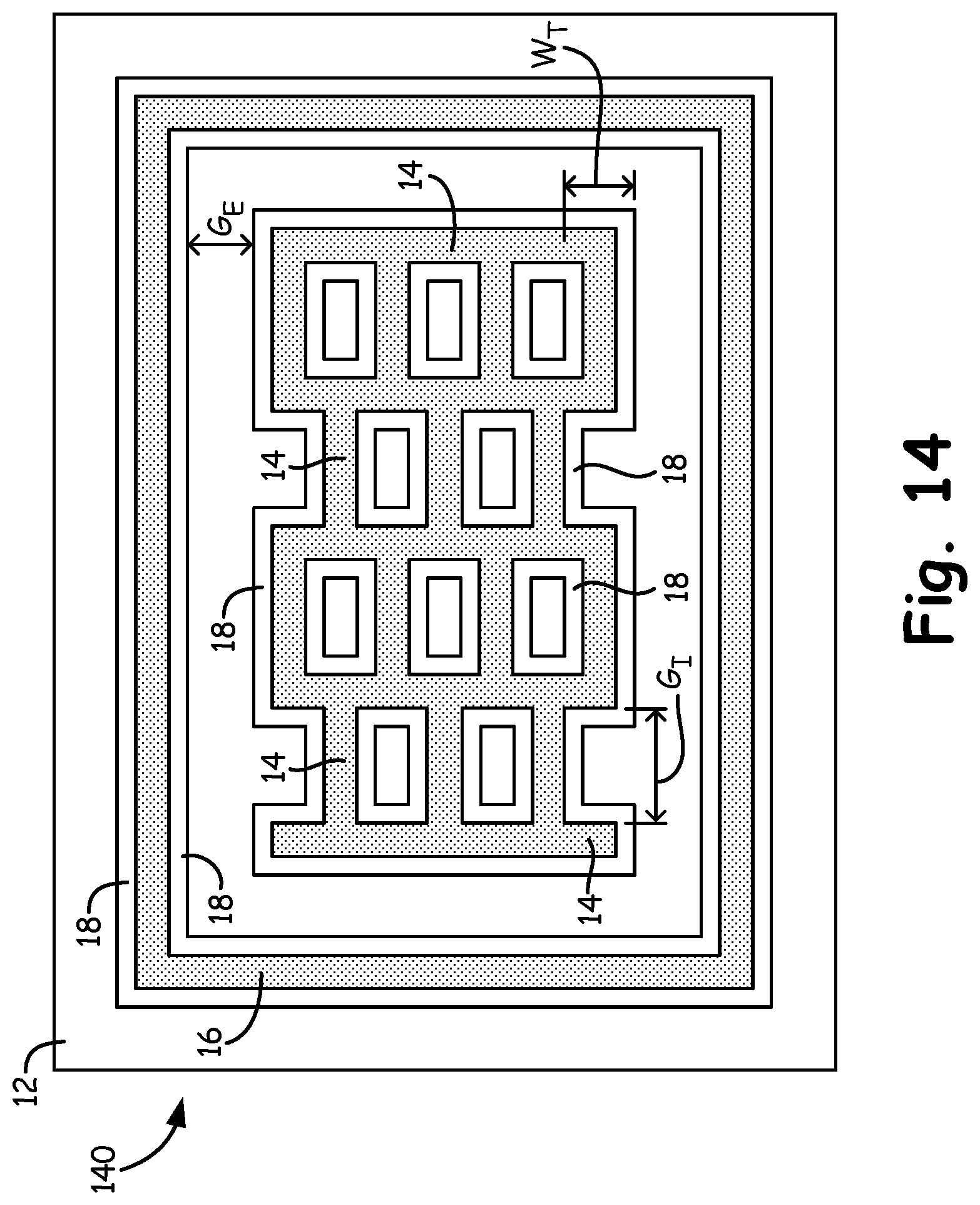
[0043] FIG. 14 is a top plan view of MOSFET device 140 formed as a trench semiconductor device according to another embodiment of the present invention. MOSFET device 140 includes semiconductor layer 12, a plurality of interior trenches 14 formed in semiconductor layer 12, and exterior trench 16 formed in semiconductor layer 12. Interior trenches 14 and exterior trench 16 are lined with dielectric material 18, such as silicon dioxide in some embodiments, and the dielectric lined trenches are filled with a conductive material (not shown) such as a metal or doped polysilicon. Interior trenches 14 are formed in an offset grid pattern enclosed by exterior trench 16, as shown in FIG. 14. In the grid pattern, the vertical legs of interior trenches 14 are separated from one another by interior gap distance G.sub.I, as are adjacent horizontal legs of interior trenches 14. Each leg of interior trenches 14 has a trench width W.sub.T, and interior trenches 14 are spaced from exterior trench 16 by gap distance G.sub.E.
[0044] In an exemplary embodiment, gap distance G.sub.I may be about 4.5 .mu.m, trench width W.sub.T may be about 1.4 .mu.m, and gap distance G.sub.E may be about 2 .mu.m.
[0045] FIG. 15 is a top plan view of MOSFET device 150 formed as a trench semiconductor device according to another embodiment of the present invention. MOSFET device 150 includes semiconductor layer 12, a plurality of interior trenches 14 formed in semiconductor layer 12, and exterior trench 16 formed in semiconductor layer 12. Interior trenches 14 and exterior trench 16 are lined with dielectric material 18, such as silicon dioxide in some embodiments, and the dielectric lined trenches are filled with a conductive material (not shown) such as a metal or doped polysilicon. Interior trenches 14 are formed in a honeycomb pattern enclosed by exterior trench 16, as shown in FIG. 15. In the honeycomb pattern, adjacent vertical legs of interior trenches 14 are separated from one another by interior gap distance G.sub.I. Each leg of interior trenches 14 has a trench width W.sub.T, and interior trenches 14 are spaced from exterior trench 16 by gap distance G.sub.E.
[0046] In an exemplary embodiment, trench width W.sub.T may be about 1.4 .mu.m, and gap distance G.sub.E may be about 2 .mu.m.
[0047] FIG. 16 is a top plan view of MOSFET device 160 formed as a trench semiconductor device according to another embodiment of the present invention. MOSFET device 160 includes semiconductor layer 12, a plurality of interior trenches 14 formed in semiconductor layer 12, and exterior trench 16 formed in semiconductor layer 12. Interior trenches 14 and exterior trench 16 are lined with dielectric material 18, such as silicon dioxide in some embodiments, and the dielectric lined trenches are filled with a conductive material (not shown) such as a metal or doped polysilicon. Interior trenches 14 are formed in a geometric trench pattern formed of six sided polygons and eight sided polygons enclosed by exterior trench 16, as shown in FIG. 16. In the geometric trench pattern, adjacent vertical legs of interior trenches 14 are separated from one another by interior gap distance G.sub.I. Each leg of interior trenches 14 has a trench width W.sub.T, and interior trenches 14 are spaced from exterior trench 16 by gap distance G.sub.E.
[0048] In an exemplary embodiment, trench width W.sub.T may be about 1.4 .mu.m, and gap distance G.sub.E may be about 2 .mu.m.
[0049] The embodiments of the present invention disclosed herein include geometric features that can be mixed and matched with any other disclosed embodiments. For example, the segmented outer trench 16 shown in FIG. 7 may be used with the snake trench pattern shown in FIG. 1A in an alternative embodiment. Other features may also be combined and modified to form additional alternative embodiments and configurations.
[0050] In many of the embodiments disclosed herein, modifications of the dimensions of trenches or other features, as well as of gaps between trenches or other features, are able to be modified in order to adjust the performance of the device, such as the breakdown voltage of the device. Examples of such modifications and the resulting performance adjustments are discussed specifically with respect to the embodiments of FIGS. 7 and 8, and modifications to others of the disclosed embodiments will also result in performance adjustments that may be selected and optimized for a particular application.
[0051] While the invention has been described with reference to an exemplary embodiment(s), it will be understood by those skilled in the art that various changes may be made and equivalents may be substituted for elements thereof without departing from the scope of the invention. In addition, many modifications may be made to adapt a particular situation or material to the teachings of the invention without departing from the essential scope thereof. Therefore, it is intended that the invention not be limited to the particular embodiment(s) disclosed, but that the invention will include all embodiments falling within the scope of the description herein.
* * * * *
D00000
D00001
D00002
D00003
D00004
D00005
D00006
D00007
D00008
D00009
D00010
D00011
D00012

D00013

D00014

D00015

D00016

D00017
D00018

D00019

XML
uspto.report is an independent third-party trademark research tool that is not affiliated, endorsed, or sponsored by the United States Patent and Trademark Office (USPTO) or any other governmental organization. The information provided by uspto.report is based on publicly available data at the time of writing and is intended for informational purposes only.
While we strive to provide accurate and up-to-date information, we do not guarantee the accuracy, completeness, reliability, or suitability of the information displayed on this site. The use of this site is at your own risk. Any reliance you place on such information is therefore strictly at your own risk.
All official trademark data, including owner information, should be verified by visiting the official USPTO website at www.uspto.gov. This site is not intended to replace professional legal advice and should not be used as a substitute for consulting with a legal professional who is knowledgeable about trademark law.