Method For Depositing A Group Iv Semiconductor And Related Semiconductor Device Structures
Tolle; John ; et al.
U.S. patent application number 16/679885 was filed with the patent office on 2020-03-12 for method for depositing a group iv semiconductor and related semiconductor device structures. The applicant listed for this patent is ASM IP Holding B.V.. Invention is credited to Joe Margetis, John Tolle.
| Application Number | 20200083375 16/679885 |
| Document ID | / |
| Family ID | 65023461 |
| Filed Date | 2020-03-12 |
| United States Patent Application | 20200083375 |
| Kind Code | A1 |
| Tolle; John ; et al. | March 12, 2020 |
METHOD FOR DEPOSITING A GROUP IV SEMICONDUCTOR AND RELATED SEMICONDUCTOR DEVICE STRUCTURES
Abstract
A method for depositing a Group IV semiconductor on a surface of a substrate is disclosed. The method may include: providing a substrate within a reaction chamber and heating the substrate to a deposition temperature. The methods may further include: exposing the substrate to at least one Group IV precursor and exposing the substrate to at least one Group IIIA dopant precursor; wherein the at least one Group IIIA dopant precursor comprises a borohydride, an organic borohydride, a halide, or an organohalide. Semiconductor device structures including a Group IV semiconductor deposited by the methods of the disclosure are also provided.
| Inventors: | Tolle; John; (Gilbert, AZ) ; Margetis; Joe; (Gilbert, AZ) | ||||||||||
| Applicant: |
|
||||||||||
|---|---|---|---|---|---|---|---|---|---|---|---|
| Family ID: | 65023461 | ||||||||||
| Appl. No.: | 16/679885 | ||||||||||
| Filed: | November 11, 2019 |
Related U.S. Patent Documents
| Application Number | Filing Date | Patent Number | ||
|---|---|---|---|---|
| 15985298 | May 21, 2018 | 10541333 | ||
| 16679885 | ||||
| 62534618 | Jul 19, 2017 | |||
| Current U.S. Class: | 1/1 |
| Current CPC Class: | H01L 29/167 20130101; H01L 29/66795 20130101; H01L 21/02529 20130101; H01L 29/45 20130101; H01L 29/7851 20130101; H01L 21/0262 20130101; H01L 29/7848 20130101; H01L 29/0847 20130101; H01L 29/36 20130101; H01L 21/02579 20130101; H01L 29/165 20130101; H01L 29/785 20130101; H01L 21/02532 20130101; H01L 21/02535 20130101 |
| International Class: | H01L 29/78 20060101 H01L029/78; H01L 29/36 20060101 H01L029/36; H01L 29/167 20060101 H01L029/167; H01L 21/02 20060101 H01L021/02; H01L 29/08 20060101 H01L029/08; H01L 29/165 20060101 H01L029/165 |
Claims
1. A semiconductor device structure, comprising: a substrate; and a Group IV semiconductor disposed on a surface of the substrate, wherein the Group IV semiconductor comprises at least one of silicon (Si), germanium (Ge), silicon germanium (Si.sub.1-xGe.sub.x), silicon germanium carbide (Si.sub.1-x-yGe.sub.xC.sub.y), germanium tin (Ge.sub.1-xSn.sub.x), germanium silicon tin (Ge.sub.1-x-ySi.sub.xSn.sub.y), germanium silicon tin carbide (Ge.sub.1-x-ySi.sub.xSn.sub.yC.sub.x), silicon tin (Si.sub.1-xSn.sub.x), silicon tin carbide (Si.sub.1-x-ySn.sub.xC.sub.y), or silicon carbide (Si.sub.1-xC.sub.x), and wherein the Group IV semiconductor is formed by: providing the substrate within a reaction chamber; heating the substrate to a deposition temperature; exposing the substrate to at least one Group IV precursor; and exposing the substrate to at least one Group IIIA dopant precursor, wherein the at least one Group IIIA dopant precursor comprises at least one of: a borohydride, an organic borohydride, a halide, or an organohalide.
2. The semiconductor device structure of claim 1, wherein the Group IV semiconductor comprises a p-type stressor region.
3. The semiconductor device structure of claim 2, further comprising forming an electrical contact to the p-type stressor region, wherein the electrical contact has an electrical resistivity of less than 1.times.10.sup.-8 Ohmcm.sup.2.
Description
CROSS-REFERENCE TO RELATED PATENT APPLICATION
[0001] This application is a divisional of, and claims priority to and the benefit of, U.S. Ser. No. 15/985,298 filed on May 21, 2018 and entitled "METHOD FOR DEPOSITING A GROUP IV SEMICONDUCTOR AND RELATED SEMICONDUCTOR DEVICE STRUCTURES," which claims priority to and the benefit of U.S. Provisional Patent Application No. 62/534,618, filed on Jul. 19, 2017 and entitled "A METHOD FOR DEPOSITING A GROUP IV SEMICONDUCTOR AND RELATED SEMICONDUCTOR DEVICE STRUCTURES," both of which are incorporated by reference herein.
FIELD OF INVENTION
[0002] The present disclosure generally relates to methods for depositing a group IV semiconductor and related semiconductor device structures. The present disclosure also generally relates to methods of doping a group IV semiconductor and doping precursors which may be utilized for p-type doping of group IV semiconductors.
BACKGROUND OF THE DISCLOSURE
[0003] The scaling of semiconductor device structures, such as, for example, complementary metal-oxide-semiconductor (CMOS) devices, has led to significant improvements in speed and density of integrated circuits. However, conventional device scaling faces immense challenges for future technology nodes.
[0004] One approach to improve semiconductor device performance is to enhance the carrier mobility, and consequently the transistor drive current, utilizing strain induced effects. For example, it has been shown that the hole mobility may be considerably enhanced in a p-channel silicon (Si) transistor employing stressor regions, such as, stressor regions employed in the source and drain regions of the transistor structure.
[0005] The contact resistance to the active regions of a semiconductor device structure may be a concern for on-going device improvement at future technology nodes. For example, for CMOS device structures, the contact resistance may include the electrical resistance between the contact structure and one or more stressor regions comprising the source and drain regions of the transistor structure. In the case of an n-type MOS device, the stressor region may comprise a highly doped region, i.e., with a carrier density of approximately 5.times.10.sup.20 cm.sup.-3, doped with either phosphorus or arsenic. The high doping levels that may be achieved in the n-type MOS device stressor region may result in a contact resistivity as low as 0.3 m.OMEGA.-cm. However, for the p-type MOS device, the current state of the art has focused on the use of boron p-type doping utilizing a boron dopant precursor, such as, diborane (B.sub.2H.sub.6). The use of diborane (B.sub.2H.sub.6) in p-type MOS devices may result in a carrier density of approximately 1.times.10.sup.20 cm.sup.-3. Efforts to increase the p-type carrier density in p-type MOS devices by the addition of further boron may result in a decline in the crystalline quality of the doped stressor region and may not significantly contribute to the active carrier density in the p-type stressor region. Accordingly, alternative methods and precursors are desired that would enable high p-type doping densities in semiconductor materials, such as, for example, Group IV semiconductor materials.
SUMMARY OF THE DISCLOSURE
[0006] In accordance with at least one embodiment of the disclosure, a method for depositing a Group IV semiconductor on a surface of a semiconductor is disclosed. The method may comprise: providing a substrate within a reaction chamber, heating the substrate to a deposition temperature, exposing the substrate to at least one Group IV precursor, and exposing the substrate to at least one Group IIIA dopant precursor, wherein the at least one Group IIIA dopant precursor comprises a borohydride, an organic borohydride, a halide, or an organohalide. The embodiments of the disclosure may also include a semiconductor device structure which may comprise a Group IV semiconductor deposited by the methods of the disclosure.
[0007] For purposes of summarizing the invention and the advantages achieved over the prior art, certain objects and advantages of the invention have been described herein above. Of course, it is to be understood that not necessarily all such objects or advantages may be achieved in accordance with any particular embodiment of the invention. Thus, for example, those skilled in the art will recognize that the invention may be embodied or carried out in a manner that achieves or optimizes one advantage or group of advantages as taught or suggested herein without necessarily achieving other objects or advantages as may be taught or suggested herein.
[0008] All of these embodiments are intended to be within the scope of the invention herein disclosed. These and other embodiments will become readily apparent to those skilled in the art from the following detailed description of certain embodiments having reference to the attached figures, the invention not being limited to any particular embodiment(s) disclosed.
BRIEF DESCRIPTION OF THE DRAWING FIGURES
[0009] While the specification concludes with claims particularly pointing out and distinctly claiming what are regarded as embodiments of the invention, the advantages of embodiments of the disclosure may be more readily ascertained from the description of certain examples of the embodiments of the disclosure when read in conjunction with the accompanying drawing, in which:
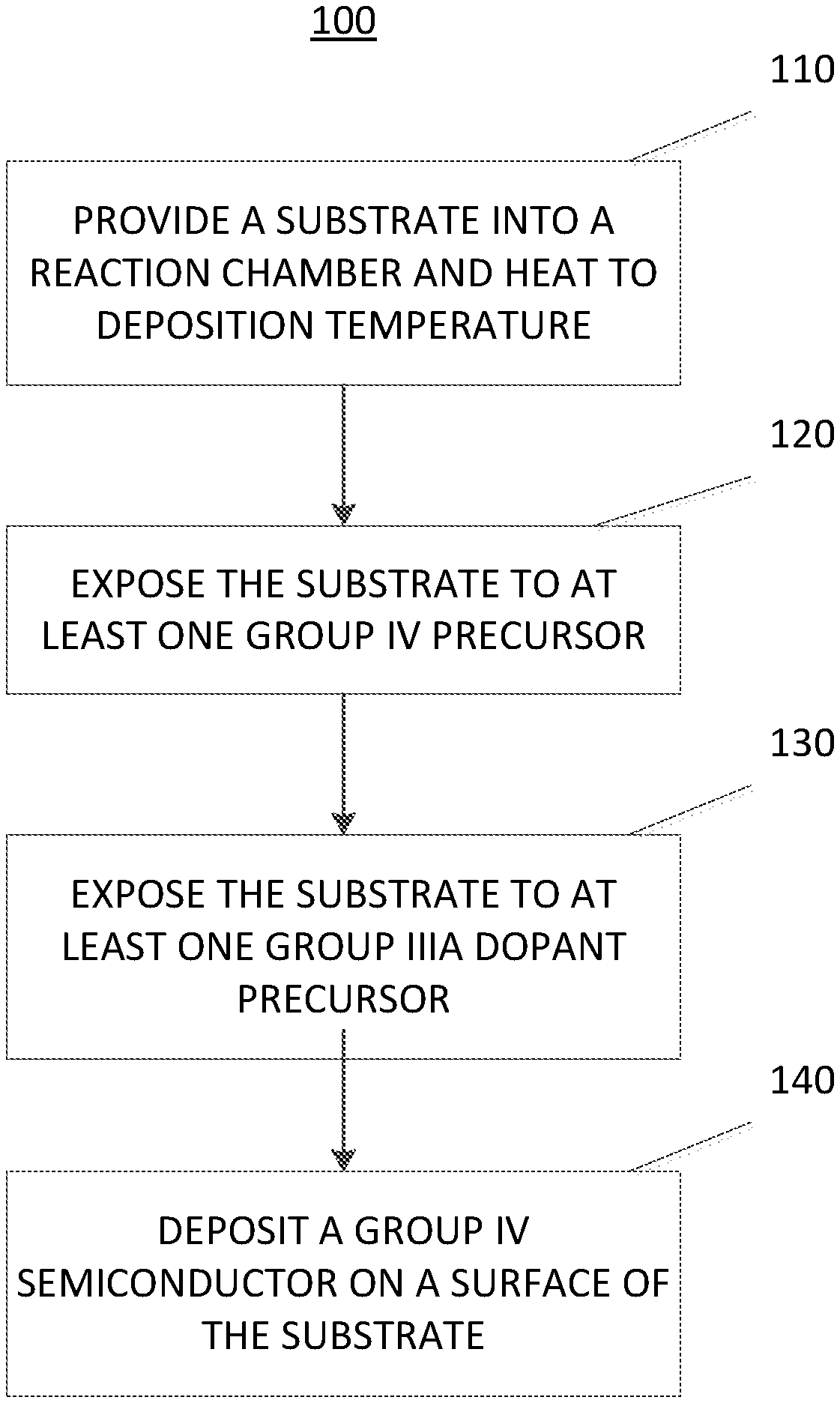
[0010] FIG. 1 illustrates a process flow diagram illustrating an exemplary deposition method in accordance with embodiments of the disclosure; and
[0011] FIG. 2 illustrates a schematic diagram of a semiconductor device structure including a p-type doped Group IV semiconductor deposited in accordance with embodiments of the disclosure.
[0012] It will be appreciated that elements in the figures are illustrated for simplicity and clarity and have not necessarily been drawn to scale. For example, the dimensions of some of the elements in the figures may be exaggerated relative to other elements to help improve understanding of illustrated embodiments of the present disclosure.
DETAILED DESCRIPTION OF EXEMPLARY EMBODIMENTS
[0013] Although certain embodiments and examples are disclosed below, it will be understood by those in the art that the invention extends beyond the specifically disclosed embodiments and/or uses of the invention and obvious modifications and equivalents thereof. Thus, it is intended that the scope of the invention disclosed should not be limited by the particular disclosed embodiments described below.
[0014] As used herein, the term "substrate" may refer to any underlying material or materials that may be used, or upon which, a device, a circuit or a film may be formed.
[0015] As used herein, the term "Group IV semiconductor" may refer to a semiconductor material comprising at least one of carbon (C), silicon (Si), germanium (Ge), tin (Sn), or alloys thereof.
[0016] As used herein, the term "Group IIIA dopant precursor" may refer to dopant precursor comprising at least one of boron (B), aluminum (Al), gallium (Ga), or indium (In).
[0017] The embodiments of the disclosure may include methods for depositing a Group IV semiconductor and particularly methods for depositing Group IV semiconductors comprising a Group IIIA dopant. As a non-limiting example of the embodiments of the disclosure, the methods may include, depositing a Group IV semiconductor layer comprising a Group IIIA dopant, such as, for example, a dopant comprising at least one of: boron (B), aluminum (Al), gallium (Ga), or indium (In). The methods of the disclosure utilize novel Group IIIA dopant precursors, which may enable high active carrier concentrations up to, for example, active carrier concentrations of greater than approximately 1.times.10.sup.20 cm.sup.-3. The methods of the disclosure may also utilize novel Group IIIA dopant precursors for achieving high active p-type carrier concentrations in Group IV semiconductors, including Group IIIA dopant precursors, such as, for example, one or more of borohydrides, organic borohydrides, halides, or organohalides. The novel Group IIIA dopant precursors described herein for achieving high active p-type carrier concentrations in Group IV semiconductors may not only provide high carrier concentrations, but also retain the crystalline quality of the Group IV semiconductor. For example, Group IV semiconductors are most commonly doped with boron, utilizing diborane (B.sub.2H.sub.6). However, the addition of boron to a stressor region, such as, for example, to a silicon germanium stressor region, may decrease the overall strain imposed by the stressor region, resulting in a reduction in carrier mobility and consequently the semiconductor device performance. The novel Group IIIA dopants described herein also allow for a reduction in electrical contact resistance with a semiconductor device structure, such as, for example, a transistor structure.
[0018] The methods of the disclosure may be understood with reference to FIG. 1 which illustrates a non-limiting example embodiment of a method for forming a Group IV semiconductor. For example, FIG. 1 may illustrate a method 100 for forming a Group IV semiconductor, which may comprise a process block 110 wherein a substrate may be provided into a reaction chamber and the substrate may be heated to a deposition temperature within the reaction chamber. As a non-limiting example, the reaction chamber may comprise a reaction chamber of a chemical vapor deposition system. Embodiments of the present disclosure may be performed in a chemical vapor deposition system available from ASM International N.V. under the name Intrepid.TM. XP or Epsilon.RTM.. However, it is also contemplated that other reaction chambers, such as, for example, atomic layer deposition reaction chambers, and alternative chemical vapor deposition system from other manufacturers may also be utilized to perform the embodiments of the present disclosure.
[0019] In some embodiments of the disclosure, the substrate may comprise, a planar substrate or a patterned substrate. Patterned substrates may comprise substrates that may include semiconductor device structures formed into or onto a surface of the substrate, for example, the patterned substrates may comprise partially fabricated semiconductor device structures such as transistors and memory elements. The substrate may contain monocrystalline surfaces and/or one or more secondary surfaces that may comprise a non-monocrystalline surface, such as a polycrystalline surface and an amorphous surface. Monocrystalline surfaces may comprise, for example, one or more of: silicon (Si), silicon germanium (SiGe), germanium tin (GeSn), or germanium (Ge). Polycrystalline or amorphous surfaces may include dielectric materials, such as oxides, oxynitrides, or nitrides, including, for example, silicon oxides and silicon nitrides.
[0020] With continued reference to FIG. 1, the method 100 may continue by heating the substrate to a desired deposition temperature within a reaction chamber. In some embodiments of the disclosure, the method 100 may comprise heating the substrate to a temperature of less than approximately 700.degree. C., or to a temperature of less than approximately 600.degree. C., or to a temperature of less than approximately 500.degree. C., or to a temperature of less than approximately 400.degree. C., or even to a temperature of less than approximately 300.degree. C. For example, in some embodiments of the disclosure, heating the substrate to a deposition temperature may comprise heating the substrate to a temperature of between approximately 280.degree. C. and approximately 700.degree. C.
[0021] Once the substrate is heated to the desired deposition temperature, the method 100 may continue by exposing the substrate to one or more deposition precursors, which may comprise one or more precursors for depositing a Group IV semiconductor and may also comprise one or more precursors for doping the Group IV semiconductor with one or more p-type dopants.
[0022] Therefore, the methods of the disclosure may comprise exposing the substrate to at least one Group IV precursor, as illustrated by a process block 120 of FIG. 1. In some embodiments, exposing the substrate to at least one Group IV precursor may further comprise selecting the at least one Group IV precursor as one of: silane (SiH.sub.4), disilane (Si.sub.2H.sub.6), trisilane (Si.sub.3H.sub.8), tetrasilane (Si.sub.4H.sub.10), isopentasilane (Si.sub.5H.sub.12), neopentasilane (Si.sub.5H.sub.12), dichlorosilane (DCS), germane (GeH.sub.4), digermane (Ge.sub.2H.sub.6), trigermane (Ge.sub.3H.sub.8), germylsilane (GeH.sub.6Si), tin tetrachloride (SnCl.sub.4), or methylsilane (CH.sub.3--SiH.sub.3).
[0023] In some embodiments, a single Group IV precursor may be utilized during the deposition process, for example, a single Group IV precursor may be utilized when the Group IV semiconductor to be deposited comprises silicon (Si) or germanium (Ge). In some embodiments, two or more Group IV precursors may be utilized during the deposition process, for example, two or more Group IV precursors may be utilized when the Group IV semiconductor to be deposited comprises a Group IV semiconductor alloy, including, but not limited to, silicon germanium carbide (Si.sub.1-x-yGe.sub.xC.sub.y), germanium tin (Ge.sub.1-xSn.sub.x), germanium silicon tin (Ge.sub.1-x-ySi.sub.xSn.sub.y), germanium silicon tin carbide (Ge.sub.1-x-ySi.sub.xSn.sub.yC.sub.x), silicon tin (Si.sub.1-xSn.sub.x), silicon tin carbide (Si.sub.1-x-ySn.sub.xC.sub.y), or silicon carbide (Si.sub.1-xC.sub.x).
[0024] The deposition process for depositing a Group IV semiconductor may also comprise, exposing the substrate to at least one Group IIIA dopant precursor. For example, in some embodiments of the disclosure the deposition method 100 as illustrated in FIG. 1, may comprise exposing the substrate to at least one Group IV precursor whilst simultaneously exposing the substrate to at least one Group IIIA dopant precursor, i.e., the Group IV precursor and the Group IIIA dopant precursor are co-flowed into the reaction chamber and react/decompose over a surface of the substrate disposed with the reaction chamber. The co-flow of the one or more Group IV precursors and the one or more Group IIIA dopant precursors into the reaction chamber may be utilized to enable the dopant species to be incorporated into the Group IV semiconductor as it is deposited.
[0025] In some embodiments, exposing the substrate to at least one Group IIIA dopant precursor may comprise exposing the substrate to at least one of a borohydride, an organic borohydride, a halide, or an organohalide.
[0026] In some embodiments of the disclosure, exposing the substrate to at least one Group IIIA dopant precursor may comprise exposing the substrate to at least one or more borohydrides comprising gallium borohydride (Ga(BH.sub.4).sub.3), aluminum borohydride (Al(BH.sub.4).sub.3), or indium borohydride (In(BH.sub.4).sub.3). In alternative embodiments of the disclosure, exposing the substrate to at least one Group IIIA dopant precursor may comprise, selecting the borohydride to comprise a borohydride having the formula Y.sub.xM(BH.sub.4).sub.3-x, wherein Y is independently chosen from hydrogen, deuterium, chlorine, bromine, and iodine; M is Group IIIA metal independently chosen from gallium, aluminum, and indium; and x is an integer from 0-2.
[0027] In some embodiments of the disclosure, exposing the substrate to at least one Group IIIA dopant precursor may comprise exposing the substrate to one or more organic borohydrides having the general formula R.sub.xM(BH.sub.4).sub.3-x, wherein R is independently chosen from CH.sub.3, C.sub.2H.sub.5, C.sub.6H.sub.5, CF.sub.3SO.sub.3, and NH.sub.2; M is a Group IIIA metal independently chosen from gallium, aluminum and indium; and x is integer from 1-3.
[0028] In some embodiments of the disclosure, exposing the substrate to at least one Group IIIA dopant precursors may comprise exposing the substrate to one or more halides having the general formula Z.sub.xMY.sub.3-x, wherein Z is independently chosen from hydrogen, deuterium, chlorine, bromine, and iodine; M is Group IIIA metal independently chosen from gallium, aluminum, and indium; Y is a halide independently chosen from chlorine, bromine, and iodine; and x is an integer from 0-3. In some embodiments of the disclosure, the halide dopant may comprise a dimer structure and therefore methods may comprise selecting the halide to comprise a halide having the formula (Z.sub.xMY.sub.3-x).sub.2, wherein Z is independently chosen from hydrogen, deuterium, chlorine, bromine, and iodine; M is Group IIIA metal independently chosen from gallium, aluminum, and indium; Y is a halide independently chosen from chlorine, bromine, and iodine; and x is an integer from 0-3.
[0029] In some embodiments of the disclosure, exposing the substrate to at least one Group IIIA dopant precursors may comprise selecting the Group IIIA dopant to comprise one or more organohalides and may further comprise selecting the one or more organohalides to comprise, an organohalide having the general formula R.sub.xMY.sub.3-x, wherein R is independently chosen from CH.sub.3, C.sub.2H.sub.5, C.sub.6H.sub.5, CF.sub.3SO.sub.3, and NH.sub.2; M is group IIIA metal independently chosen from gallium, aluminum, and indium; Y is a halide independently chosen from chlorine, bromine, and iodine; and x is an integer from 0-3.
[0030] The selection of Group IIIA dopant precursors comprising an organic component may be further beneficial in the deposition of Group IV semiconductors. For example, carbon incorporation into a Group IV semiconductor may further increase the strain in the Group IV semiconductor being deposited. Therefore, in some embodiments of the disclosure, exposing the substrate to at least one Group IIIA precursor further comprises exposing the substrate to at least one of an organic borohydride or an organohalide. In further embodiments, exposing the substrate to at least one of an organic borohydride or an organohalide further comprises incorporating carbon into the deposited Group IV semiconductor, the atomic percentage (at-%) of carbon in the Group IV semiconductor being greater than approximately 0.5% at-%.
[0031] In some embodiments of the disclosure, two or more dopant species may be incorporated into the deposited Group IV semiconductor. For example, in some embodiments, exposing the substrate to at least one Group IIIA dopant precursor further comprises, exposing the substrate to at least one of a borohydride or an organic borohydride. In embodiments utilizing borohydrides or organic borohydrides, the dopant precursor contains boron (B) in addition to a further Group IIIA dopant (e.g., gallium, aluminum, or indium). Therefore utilizing borohydrides or organic borohydrides comprises incorporating a boron dopant and a further Group IIIA dopant into the deposited Group IV semiconductor. Such methods may be utilized to further increase the dopant concentration in the Group IV semiconductor without a corresponding decrease in crystalline quality of the Group IV semiconductor.
[0032] The embodiments of the disclosure may continue with a process block 140 of FIG. 1, wherein a Group IV semiconductor may be deposited on a surface of the substrate disposed within the reaction chamber. In some embodiments, depositing a Group IV semiconductor on the surface of the substrate comprises, depositing at least one of silicon (Si), germanium (Ge), silicon germanium (Si.sub.1-xGe.sub.x), silicon germanium carbide (Si.sub.1-x-yGe.sub.xC.sub.y), germanium tin (Ge.sub.1-xSn.sub.x), germanium silicon tin (Ge.sub.1-x-ySi.sub.xSn.sub.y), germanium silicon tin carbide (Ge.sub.1-x-ySi.sub.xSn.sub.yC.sub.x), silicon tin (Si.sub.1-xSn.sub.x), silicon tin carbide (Si.sub.1-x-ySn.sub.xC.sub.y), or silicon carbide (Si.sub.1-xC.sub.x).
[0033] The methods of the disclosure allow the Group IV semiconductor to be deposited with a high concentration of p-type dopants without reducing the crystalline quality of the Group IV semiconductor. For example, in some embodiment, depositing a Group IV semiconductor on the surface of the substrate further comprises, depositing the Group IV semiconductor with a doping concentration of greater than approximately 1.times.10.sup.20 carriers per cubic centimeter, or greater than approximately 2.5.times.10.sup.20 carriers per cubic centimeter, or even greater than approximately 5.times.10.sup.20 carriers per cubic centimeter.
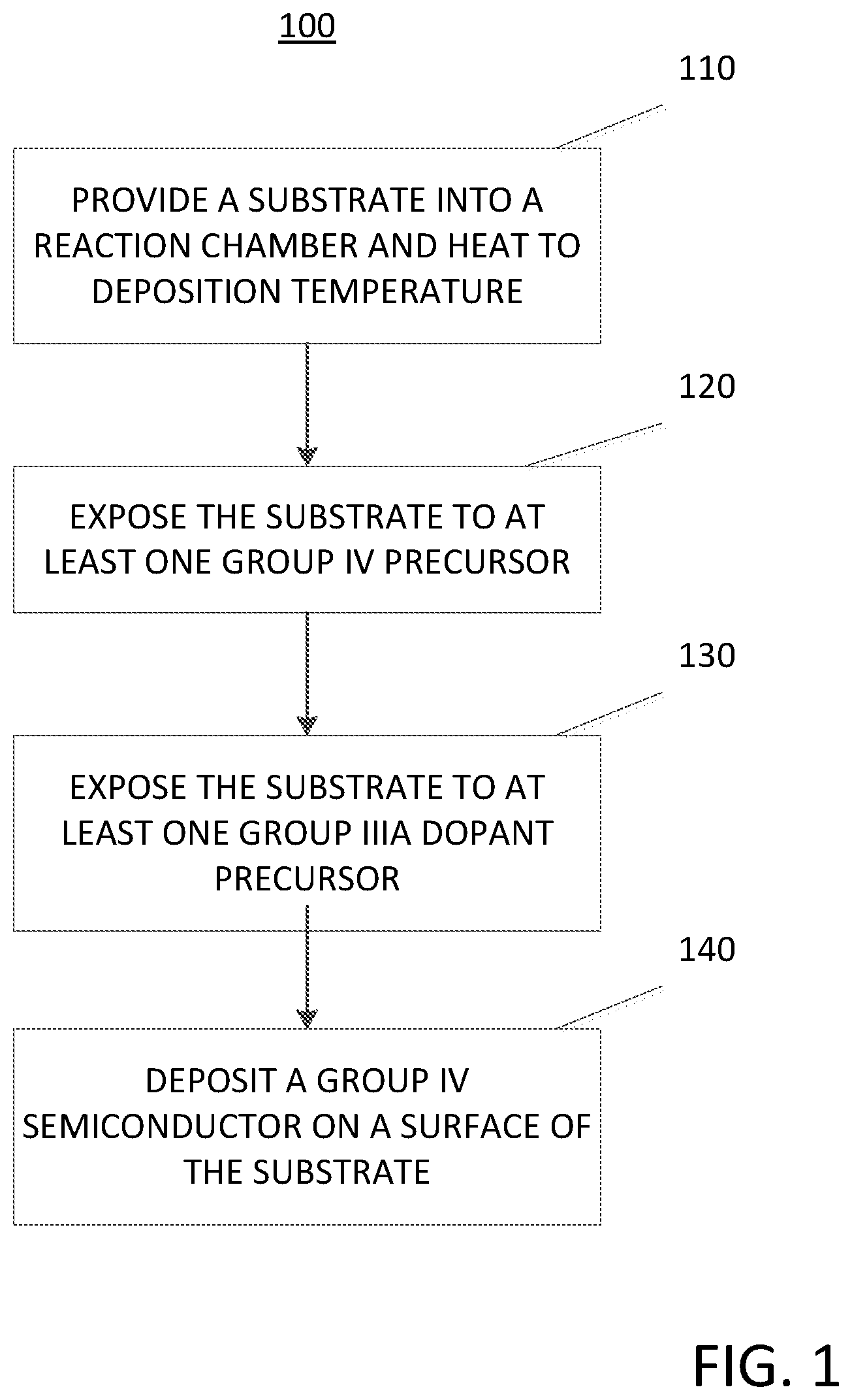
[0034] The embodiments of the disclosure may also provide semiconductor device structures comprising a Group IV semiconductor deposited by the methods described herein. For example, FIG. 2 illustrates a non-limiting example of a semiconductor device structure 200, wherein the semiconductor device structure 200 comprises a double gate MOSFET, commonly referred to as a FinFET. The semiconductor device structure 200 may comprise a substrate 202, which may comprise a bulk silicon (Si) substrate. The substrate 202 may be doped either with p-type dopants (for NMOS type FinFET devices) or with n-type dopants (for PMOS type FinFET devices). In the non-limiting example semiconductor device structure of FIG. 2 the substrate 200 may comprise n-type dopants and the semiconductor device structure 200 may comprise a PMOS FinFET.
[0035] The semiconductor device structure 200 may also comprise isolation regions 204, which may comprise shallow trench isolation (STI) regions. The semiconductor device structure 200 may also comprise a Fin structure 206 extending over the top surfaces of the isolation regions 204. A gate dielectric may be disposed over the sidewalls of the Fin structure 206 (not shown) and the gate dielectric may comprise a silicon oxide or a high-k dielectric material. A gate electrode 208 may be disposed on the gate dielectric for providing electrical contact to the channel region within the Fin structure 206. The semiconductor device structure 200 may also comprise gate spacers 210, which are disposed on the sidewalls of the gate electrode 208.
[0036] In some embodiments of the disclosure, the semiconductor device structure 200 may further comprise p-type Group IV semiconductor stressor regions 212A and 212B deposited over the source and drain regions of the FinFET device. It should be noted that the p-type stressor regions 212A and 212B may comprise a number of facets that may result due to the difference in growth rates on the different facets of the Fin structure 206. In non-limiting example embodiments of the disclosure, the p-type stressor regions 212A and 212B may be deposited utilizing the embodiments of the disclosure described herein. For example, the p-type stressor regions 212A and 212B may comprise silicon germanium (Si.sub.1-xGe.sub.x) wherein the germanium composition in the silicon germanium stressor regions may be greater than approximately x>0.2, or greater than approximately x>0.50, or greater than approximately x>0.75, or even approximately x=1.0. In addition, the p-type stressor regions 212A and 212B may be doped according to the embodiments of the current disclosure and therefore the p-type stressor regions 212A and 212B may comprise a p-type doping concentration of greater than approximately 1.times.10.sup.20 carriers per cubic centimeter, or greater than approximately 2.5.times.10.sup.20 carriers per cubic centimeter, or even greater than approximately 5.times.10.sup.20 carriers per cubic centimeter.
[0037] In some embodiments of the disclosure, an electrical contact may be made to the p-type Group IV semiconductor stressor regions 212A and 212B deposited over the source and drain regions of the FinFET device illustrated in FIG. 2. In some embodiments, the electrical contact (not shown) may comprise a silicide, such as, for example, a titanium silicide (TiSi.sub.2). The embodiments of the disclosure allow for a high concentration of active p-type carriers in the source and drain stressor regions 212A and 212B which in turn may result in a reduction in the electrical contact resistance to the stressor regions. For example, the methods of the disclosure may comprise forming an electrical contact to the p-type stressor regions 212A and 212B, wherein the electrical contact has an electrical resistivity of less than 1.times.10.sup.-9 Ohmcm.sup.2, or less than 5.times.10.sup.-9 Ohmcm.sup.2, or even less than 1.times.10.sup.-8 Ohmcm.sup.2.
[0038] It should be noted that a non-limiting example embodiment given herein relates to p-type stressor regions formed over the source and drain regions of a FinFET device. However, the embodiments of the disclosure may be utilized for other purposes, for example, the p-type Group IV semiconductors deposited by the embodiments of the disclosure may be utilized to induce stress in other areas of a device structure, for example, by depositing a p-type stressor region over the channel region of a transistor to thereby induce strain directly in the channel region of the transistor device structure.
[0039] The example embodiments of the disclosure described above do not limit the scope of the invention, since these embodiments are merely examples of the embodiments of the invention, which is defined by the appended claims and their legal equivalents. Any equivalent embodiments are intended to be within the scope of this invention. Indeed, various modifications of the disclosure, in addition to those shown and described herein, such as alternative useful combination of the elements described, may become apparent to those skilled in the art from the description. Such modifications and embodiments are also intended to fall within the scope of the appended claims.
* * * * *
D00000
D00001
D00002
XML
uspto.report is an independent third-party trademark research tool that is not affiliated, endorsed, or sponsored by the United States Patent and Trademark Office (USPTO) or any other governmental organization. The information provided by uspto.report is based on publicly available data at the time of writing and is intended for informational purposes only.
While we strive to provide accurate and up-to-date information, we do not guarantee the accuracy, completeness, reliability, or suitability of the information displayed on this site. The use of this site is at your own risk. Any reliance you place on such information is therefore strictly at your own risk.
All official trademark data, including owner information, should be verified by visiting the official USPTO website at www.uspto.gov. This site is not intended to replace professional legal advice and should not be used as a substitute for consulting with a legal professional who is knowledgeable about trademark law.