Fin Structure Of Fin Field Effect Transistor
YUAN; Feng ; et al.
U.S. patent application number 16/511719 was filed with the patent office on 2019-11-07 for fin structure of fin field effect transistor. The applicant listed for this patent is Taiwan Semiconductor Manufacturing Co., Ltd.. Invention is credited to Chang-Yun CHANG, Hung-Ming CHEN, Tsung-Lin LEE, Clement Hsingjen WANN, Feng YUAN.
| Application Number | 20190341473 16/511719 |
| Document ID | / |
| Family ID | 43755880 |
| Filed Date | 2019-11-07 |


View All Diagrams
| United States Patent Application | 20190341473 |
| Kind Code | A1 |
| YUAN; Feng ; et al. | November 7, 2019 |
FIN STRUCTURE OF FIN FIELD EFFECT TRANSISTOR
Abstract
The fin structure includes a first portion and a second, lower portion separated at a transition. The first portion has sidewalls that are substantially perpendicular to the major surface of the substrate. The lower portion has tapered sidewalls on opposite sides of the upper portion and a base having a second width larger than the first width.
| Inventors: | YUAN; Feng; (Hsinchu City, TW) ; CHEN; Hung-Ming; (Hsinchu County, TW) ; LEE; Tsung-Lin; (Hsinchu City, TW) ; CHANG; Chang-Yun; (Taipei, TW) ; WANN; Clement Hsingjen; (Carmel, NY) | ||||||||||
| Applicant: |
|
||||||||||
|---|---|---|---|---|---|---|---|---|---|---|---|
| Family ID: | 43755880 | ||||||||||
| Appl. No.: | 16/511719 | ||||||||||
| Filed: | July 15, 2019 |
Related U.S. Patent Documents
| Application Number | Filing Date | Patent Number | ||
|---|---|---|---|---|
| 15339258 | Oct 31, 2016 | 10355108 | ||
| 16511719 | ||||
| 12766233 | Apr 23, 2010 | 9484462 | ||
| 15339258 | ||||
| 61245485 | Sep 24, 2009 | |||
| Current U.S. Class: | 1/1 |
| Current CPC Class: | H01L 29/7853 20130101; H01L 29/66795 20130101; H01L 21/308 20130101; H01L 29/66621 20130101; H01L 29/7851 20130101; H01L 21/3065 20130101 |
| International Class: | H01L 29/66 20060101 H01L029/66; H01L 29/78 20060101 H01L029/78; H01L 21/308 20060101 H01L021/308 |
Claims
1. A semiconductor device comprising: a first fin structure extending from a first substrate surface of a substrate and having a top surface and two opposing sidewalls wherein each sidewall has a first portion and a second portion, the second portion below and contiguous with the first portion, and wherein the first portion is perpendicular to the first substrate surface, and the second portion being disposed at an angle between 85 degrees and 60 degrees from the first substrate surface and wherein the second portion is further curved proximate the first substrate surface such that a slope of the second portion continually decreases from a transition location with the first portion to the first substrate surface; and an isolation structure having a top surface, the isolation structure being positioned between the first fin structure and an adjacent second fin structure, and wherein the top surface of the isolation structure is disposed above the transition location.
2. The semiconductor device of claim 1, wherein the first fin structure includes a third portion above the first portion and extending from the first portion to the top surface of the first fin structure.
3. The semiconductor device of claim 1, wherein the first fin structure has a first width at the top surface, and the first width is in a range of about 5 nanometers to about 40 nanometers.
4. The semiconductor device of claim 3, wherein the top surface of the first fin structure having the first width is planar.
5. The semiconductor device of claim 1, wherein the first fin structure has a first width at the top surface, a second width proximate to the first substrate surface, and a ratio of the first width to the second width is from about 0.3 to about 0.5.
6. The semiconductor device of claim 1, wherein a second distance from the transition location to the top surface of the first fin structure is in a range of about 40 nanometers to about 100 nanometers.
7. The semiconductor device of claim 6, wherein a third distance between a base of the first fin structure and the top surface of the first fin structure is in a range of about 100 nanometers to about 300 nanometers.
8. The semiconductor device of claim 6, wherein a ratio of the second distance to a third distance between a base of the first fin structure and the top surface is from about 0.15 to about 0.3.
9. The semiconductor device of claim 1, wherein a first distance from the top surface of the isolation structure to the top surface of the first fin structure is in a range of about 15 nanometers to about 45 nanometers.
10. The semiconductor device of claim 1, further comprising: a gate structure on the top surface of the isolation structure.
11. A fin field effect transistor comprising: a fin structure extending above a substrate surface, the fin structure comprising sidewalls, the sidewalls comprising: a first portion interfacing a gate structure; a second portion below the first portion, the second portion having a first sidewall portion that is perpendicular to the substrate surface and extending from the first portion of the fin structure to a transition location; and a third portion below and contiguous with the second portion, the third portion having a second sidewall portion that is curved with a continuously decreasing slope that extends from a first direct interface with the first sidewall portion at the transition location to a second direct interface with a curved sidewall of an adjacent fin structure; a channel region within the first portion of the fin structure; a gate structure over the channel region; and an isolation structure having a top surface adjacent to the fin structure, and wherein the isolation structure interfaces the transition location.
12. The fin field effect transistor of claim 11, wherein the second portion of the fin structure has a substantially constant width.
13. The fin field effect transistor of claim 12, wherein the substantially constant width is in a range of about 5 nanometers to about 40 nanometers.
14. The fin field effect transistor of claim 11, wherein the top surface of the isolation structure is above the transition location.
15. A semiconductor device comprising: a substrate having a first substrate surface and a second substrate surface parallel to the first substrate surface; at least two fin structures between the first substrate surface and the second substrate surface, the at least two fin structures comprising sidewalls, the sidewalls comprising: an upper portion proximate to the first substrate surface having a first sidewall portion interfacing a gate structure formed thereon, a second portion below the upper portion, the second portion having a second sidewall portion that is substantially perpendicular to the first substrate surface and interfaces an isolation structure; and a lower portion proximate the second substrate surface, the lower portion having a third sidewall portion that is curved with a continuously decreasing slope extending from the first sidewall portion and a transition location to the second substrate surface, the transition location being a position at which the second sidewall portion and the third sidewall portion meet; and the isolation structure extending between the at least two fin structures; and the first, second and third sidewalls extend continuously from the first substrate surface to the second substrate surface.
16. The semiconductor device of claim 15, wherein the second portion has a substantially constant width.
17. The semiconductor device of claim 15, wherein the isolation structure interfaces the second portion and the lower portion.
18. The semiconductor device of claim 15, wherein a top surface of the isolation structure is above the transition location.
19. The semiconductor device of claim 15, wherein the third sidewall portion of the lower portion has a slope of between 85 degrees and 60 degrees.
20. The semiconductor device of claim 15, wherein the transition location is an upper most point on the lower portion that has a slope of 85 degrees with respect to the first substrate surface.
Description
CROSS-REFERENCE TO RELATED APPLICATIONS
[0001] The present application is a continuation application of U.S. application Ser. No. 15/339,258 filed Oct. 31, 2016, which is a continuation application of U.S. application Ser. No. 12/766,233, filed Apr. 23, 2010, now U.S. Pat. No. 9,484,462, titled FIN STRUCTURE OF FIN FIELD EFFECT TRANSISTOR, which claims priority of U.S. Provisional Patent Application Ser. No. 61/245,485, filed on Sep. 24, 2009. The disclosures of each of which are incorporated by reference in their entirety.
[0002] In addition, this application is also related to U.S. patent application Ser. No. 12/707,788, filed on Feb. 18, 2010, (Docket Nos. TSMC2008-0432, T5057-R007U), titled MEMORY POWER GATING CIRCUIT AND METHODS; Ser. No. 12/758,426, filed on Apr. 12, 2010, (Docket Nos. TSMC2008-0582, T5057-Y048U), titled FINFETS AND METHODS FOR FORMING THE SAME; Ser. No. 12/731,325, filed on Mar. 25, 2010, (Docket Nos. TSMC2008-0597, T5057-B033U), titled ELECTRICAL FUSE AND RELATED APPLICATIONS; Ser. No. 12/724,556, filed on Mar. 16, 2010, (Docket Nos. TSMC2008-0598, T5057-K002U), titled ELECTRICAL ANTI-FUSE AND RELATED APPLICATIONS; Ser. No. 12/757,203, filed on Apr. 9, 2010, (Docket Nos. TSMC2009-0148, T5057-Y085U), titled STI STRUCTURE AND METHOD OF FORMING BOTTOM VOID IN SAME; Ser. No. 12/797,839, filed on Jun. 10, 2010, (Docket Nos. TSMC2009-0278, T5057-K099U), titled FIN STRUCTURE FOR HIGH MOBILITY MULTIPLE-GATE TRANSISTOR; Ser. No. 12/831,842, filed on Jul. 7, 2010, (Docket Nos. TSMC2009-0343, T5057-Y093U), titled METHOD FOR FORMING HIGH GERMANIUM CONCENTRATION SiGe STRESSOR; Ser. No. 12/761,686, filed on Apr. 16, 2010, (Docket Nos. TSMC2009-0442, T5057-Y125U), titled FINFETS AND METHODS FOR FORMING THE SAME; Ser. No. 12/766,233, filed on Apr. 23, 2010, (Docket Nos. TSMC2009-0445, T5057-Y113U), titled ACCUMULATION TYPE FINFET, CIRCUITS AND FABRICATION METHOD THEREOF; Ser. No. 12/694,846, filed on Jan. 27, 2010, (Docket Nos. TSMC2009-0646, T5057-Y165), titled INTEGRATED CIRCUITS AND METHODS FOR FORMING THE SAME; Ser. No. 12/638,958, filed on Dec. 14, 2009, (Docket Nos. TSMC2009-0738, T5057-B166), titled METHOD OF CONTROLLING GATE THICKNESS IN FORMING FINFET DEVICES; Ser. No. 12/768,884, filed on Apr. 28, 2010, (Docket Nos. TSMC2010-0028, T5057-Y228), titled METHODS FOR DOPING FIN FIELD-EFFECT TRANSISTORS; Ser. No. 12/731,411, filed on Mar. 25, 2010, (Docket Nos. TSMC2010-0057, T5057-B218), titled INTEGRATED CIRCUIT INCLUDING FINFETS AND METHODS FOR FORMING THE SAME; Ser. No. 12/775,006, filed on May 6, 2010, (Docket Nos. TSMC2010-0198, T5057-Y246), titled METHOD FOR FABRICATING A STRAINED STRUCTURE; Ser. No. 12/886,713, filed Sep. 21, 2010, (Docket Nos. TSMC2010-0646, T5057-B325), titled METHOD OF FORMING INTEGRATED CIRCUITS; Ser. No. 12/941,509, filed Nov. 8, 2010, (Docket Nos. TSMC2010-0561, T5057-B337), titled MECHANISMS FOR FORMING ULTRA SHALLOW JUNCTION; Ser. No. 12/900,626, filed Oct. 8, 2010, (Docket Nos. TSMC2010-0581, T5057-B330), titled TRANSISTOR HAYING NOTCHED FIN STRUCTURE AND METHOD OF MAKING THE SAME; Ser. No. 12/903,712, filed Oct. 13, 2010, (Docket Nos. TSMC2010-0731, T5057-R350), titled FINFET AND METHOD OF FABRICATING THE SAME; 61/412,846, filed Nov. 12, 2010, (Docket Nos. TSMC2010-0839, T5057-B388PRO), 61/394,418, filed Oct. 19, 2010, (Docket Nos. TSMC2010-0926, T5057-Y351PRO), titled METHODS OF FORMING GATE DIELECTRIC MATERIAL and 61/405,858, filed Oct. 22, 2010, (Docket Nos. TSMC2010-0928, T5057-R368PRO), titled METHODS OF FORMING SEMICONDUCTOR DEVICES, which are incorporated herein by reference in their entirety.
TECHNICAL FIELD
[0003] The present invention relates generally to transistors, and more particularly to a fin field effect transistor with an isolation structure.
BACKGROUND
[0004] Semiconductor devices are used in a large number of electronic devices, such as computers, cell phones, and others. Semiconductor devices comprise integrated circuits (ICs) that are formed on semiconductor wafers by depositing many types of thin films of material over the semiconductor wafers, and patterning the thin films of material to form the integrated circuits. The ICs include field-effect transistors (FETs), such as metal-oxide-semiconductor field-effect transistors (MOSFETs).
[0005] One of the goals of the semiconductor industry is to continue shrinking the size and increasing the speed of individual MOSFETs. To achieve these goals, three dimensional (3-D) or non-planar transistor structures such as fin FETs (FINFETs), multiple gate transistors, or gate-all-around transistors are being investigated for use in sub 22 nm transistor nodes. Such transistors not only improve area density, but also improve gate control of the channel.
[0006] However, fabrication of the FINFETs is complex and requires overcoming a number of challenging problems. One of the challenges is forming recess-free isolation structures. These recesses can be formed in a dielectric material in the early stages of forming the isolation structure. FIGS. 1A-C show cross-sectional views of a plurality of conventional isolation structures 120 for FINFETs 100 having recesses 126b present in the isolation structures 120 at various stages of fabrication. FIG. 1A illustrates the plurality of isolation structures 120 may be formed by etching a substrate 102 to form a plurality of trenches 122 separating a plurality of fin structures 110, then filling the plurality of trenches 122 with a dielectric material 124 (shown in FIG. 1B), such as high-density plasma (HDP) oxides, tetraethoxysilane (TEOS) oxides, or the like. The dielectric material 124 may comprise a plurality of deep slims/recesses 126a due to the high aspect ratio of the plurality of trenches 122. FIG. 1C shows a plurality of recesses 126b in the plurality of isolation structures 120 may be formed along the plurality of deep slims/recesses 126a during and after removing the upper portions of the dielectric material 124. The plurality of recesses 126b is problematic in various respects. For example, the plurality of recesses 126b present in the plurality of isolation structures 120 can become a receptacle of polysilicon and/or metals during subsequent processing thereby increasing the likelihood of device instability and/or device failure.
[0007] Accordingly, what is needed is an isolation structure for a FINFET having no recess.
BRIEF DESCRIPTION OF THE DRAWINGS
[0008] The present disclosure is best understood from the following detailed description when read with the accompanying figures. It is emphasized that, in accordance with the standard practice in the industry, various features are not drawn to scale and are used for illustration purposes only. In fact, the dimensions of the various features may be arbitrarily increased or reduced for clarity of discussion.
[0009] FIGS. 1A-C show cross-sectional views of a plurality of conventional isolation structures for FINFETs having recesses present in the isolation structures at various stages of fabrication;
[0010] FIGS. 2A-H show schematic cross-sectional views of a substrate being processed to fabricate a plurality of FINFETs according to an embodiment, showing various stages of fabrication;
[0011] FIG. 2I shows a perspective view of the plurality of the FINFETs fabricated using the steps shown in FIG. 2A-H; and
[0012] FIG. 3A-D shows a complete FINFET device having a plurality of isolation structures fabricated using the steps shown in FIG. 2A-H, wherein FIG. 3A shows a perspective view, and wherein FIGS. 3B-D show cross-section views taken along the respective lines of FIG. 3A.
DESCRIPTION
[0013] It is understood that the following disclosure provides many different embodiments, or examples, for implementing different features of the invention. Specific examples of components and arrangements are described below to simplify the present disclosure. These are, of course, merely examples and are not intended to be limiting. For example, the formation of a first feature over or on a second feature in the description that follows may include embodiments in which the first and second features are formed in direct contact, and may also include embodiments in which additional features may be formed between the first and second features, such that the first and second features may not be in direct contact. In addition, the present disclosure may repeat reference numerals and/or letters in the various examples. This repetition is for the purpose of simplicity and clarity and does not in itself dictate a relationship between the various embodiments and/or configurations discussed. Various features may be arbitrarily drawn in different scales for the purpose of simplicity and clarity.
[0014] FIGS. 2A-H show schematic cross-sectional views of a substrate being processed to fabricate a plurality of FINFETs according to an embodiment, showing various stages of fabrication, and FIG. 2I shows a perspective view of the plurality of the FINFETs fabricated using the steps shown in FIG. 2A-H. It is understood that part of the FINFETs 200 may be fabricated with normal complementary metal-oxide-semiconductor (CMOS) technology processes, and thus some processes are briefly described herein. Also, FIGS. 2A-H are simplified for a better understanding of the inventive concepts of the present disclosure. For example, although the figures illustrate the FINFET 200, it is understood the ICs may also include a number of various devices including resistors, capacitors, inductors, fuses, etc.
[0015] Referring to FIG. 2A, the FINFETs 200 may include a semiconductor substrate 202 such as a silicon substrate. In some embodiments, the substrate 202 may alternatively include silicon germanium, gallium arsenic, or other suitable semiconductor materials. The substrate 202 may further include other features such as various doped regions, a buried layer, and/or an epitaxy layer. Furthermore, the substrate 202 may be a semiconductor on insulator such as silicon on insulator (SOI). In other embodiments, the semiconductor substrate 202 may include a doped epi layer, a gradient semiconductor layer, and/or may further include a semiconductor layer overlying another semiconductor layer of a different type such as a silicon layer on a silicon germanium layer. In other examples, a compound semiconductor substrate 202 may include a multilayer silicon structure or a silicon substrate 202 may include a multilayer compound semiconductor structure.
[0016] Still referring to FIG. 2A, a pad oxide layer 204 is formed over the top surface of the substrate 202. In some embodiments, the pad oxide layer 204 is preferably formed of silicon oxide grown by a thermal oxidation process, having a thickness of about 80 to 150 .ANG.. For example, the pad oxide layer 204 can be grown by the rapid thermal oxidation (RTO) process or in an annealing process, which include oxygen. A hardmask layer 206, for example a silicon nitride or silicon oxynitride layer, is formed over the pad oxide layer 204. The hardmask layer 206 can be deposited by, for example, a chemical vapor deposition (CVD) process, or a low pressure CVD (LPCVD) process. Preferably, in some embodiments, the formed hardmask layer 206 has a thickness of about 600 to 1500 .ANG..
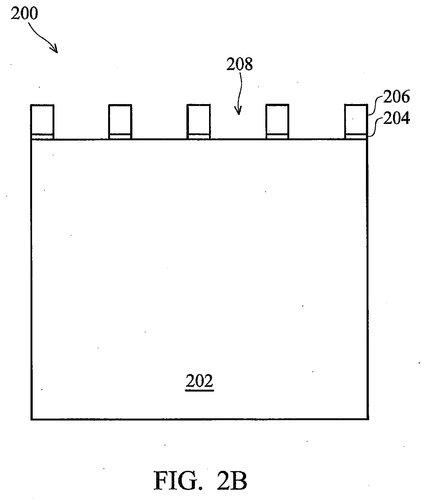
[0017] Referring to FIG. 2B, following formation of the hardmask layer 206, a patterned photo-sensitive layer (not shown) is formed on the hardmask layer 206. A reactive ion etching (RIE) or a high density plasma (HDP) process may, for example, be used to anisotropically etch through the hardmask layer 206 and the pad oxide layer 204 to form openings 208 in the hardmask layer 206 and the pad oxide layer 204, exposing a portion of the substrate 202.
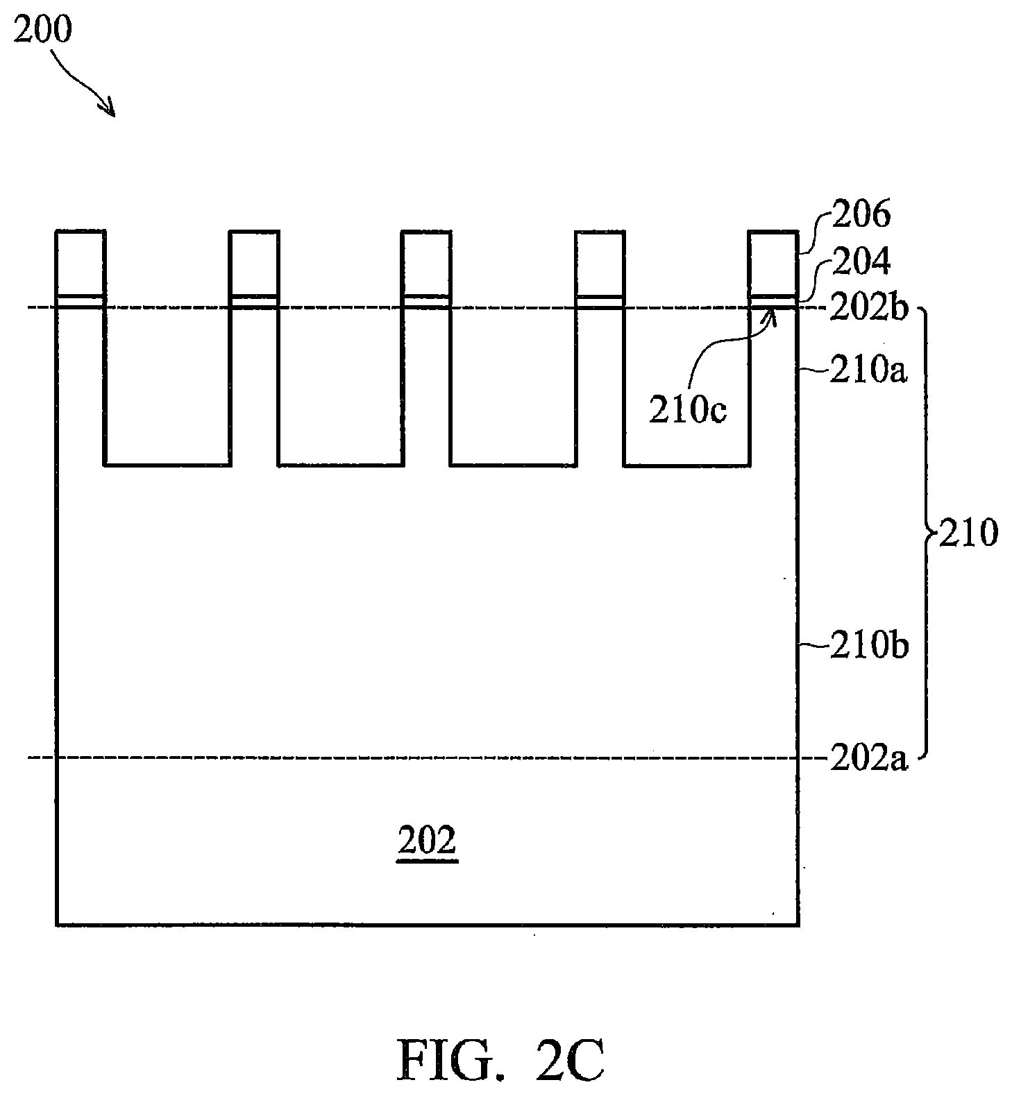
[0018] Referring to FIG. 2C, upper portions 210a of a plurality of fin structures 210 protruding from the major surface 202a of the substrate 202 may be formed by etching the substrate 202 using a first etch process. For example, the first etch process may be performed under a source power of about 550 to 650 W, a bias power of about 55 to 65 W, and a pressure of about 2 to 10 mTorr, using CH2F2, SF6, N2, and He as etching gases. The substrate 202 comprises a major surface 202a parallel to a substrate surface 202b. The upper portion 210a of each fin structure 210 has sidewalls that are substantially perpendicular to the major surface 202a of the substrate 202 and a top surface 210c.
[0019] Referring to FIG. 2D, lower portions 210b of the plurality of fin structures 210 protruding from the major surface 202a of the substrate 202 may be formed by further etching the substrate 202 using a second etch process. For example, the second etch process may be performed under a source power of about 1100 to 1250 W, a bias power of about 200 to 220 W, and a pressure of about 10 to 20 mTorr, using HBr, SF6, and He as etching gases. The upper portion 210a and the lower portion 210b of each fin structure 210 are separated at a transition location 210d at, in some embodiments, where the sidewall of the fin structure at an angle 212 of 85 degrees to the major surface 202a of the substrate 202. The lower portion 210b of each fin structure 210 has tapered sidewalls on opposite sides of the upper portion 210a and a base 210e. In some embodiments, the tapered regions of the lower portion 210b of each fin structure 210 is preferably at an angle 214 in the range of 60 degrees to 85 degrees to the major surface 202a of the substrate 202. In one embodiment, a plurality of trenches 222 formed between the tapered fin structures 210 have lower aspect ratio than the plurality of trenches 122 formed between the vertical fin structures 110. The lower aspect-ratio trenches 222 have better gap-fill performance than the higher aspect-ratio trenches 122.
[0020] Still referring to FIG. 2D, the top surface 210c of the upper portion 210a of each fin structure 210 having a first width 216a, the first width 216a is in the range of about 5 to 40 nanometers. In one embodiment, the base 210e of the lower portion 210b of each fin structure 210 having a second width 218a, the second width 218a is in the range of about 10 to 60 nanometers. In some embodiments, a ratio of the first width 216a to the second width 218a is preferably from 0.3 to 0.5.
[0021] Still referring to FIG. 2D, in some embodiments, a first offset distance 216b between the transition location 210d and the top surface 210c is in the range of about 40 to 100 nanometers. In some embodiments, a second offset distance 218b between the base 210e and the top surface 210c is in the range of about 100 to 300 nanometers. A ratio of the first offset distance 216b between the transition location 210d and the top surface 210c to the second offset distance 218b between the base 210e and the top surface 210c, in some embodiments, is preferably from 0.15 to 0.3.
[0022] Referring to FIG. 2E, following formation of the plurality of the fin structures 210, the plurality of the isolation structures 220 between the fin structures 210 may be formed in the plurality of the trenches 222. In some embodiments, a liner layer (not shown) may be formed substantially conformal over the substrate 202, including along the sidewalls of the plurality of the trenches 222. The liner layer is a dielectric layer (e.g., an oxide layer, nitride layer, oxynitride layer or combination thereof) formed by a thermal oxidation process or CVD process. Preferably, the liner layer may have a thickness of about 30 to 200 .ANG.. In some embodiments, the liner layer is provided for reducing damage on the surface of the fin structures 210 created by the trench-etch process as set forth above. In some embodiments, the liner layer is not used.
[0023] Still referring to FIG. 2E, following formation of the liner layer, a dielectric material 224 is formed over the liner layer to a sufficient thickness within and above the plurality of the trenches 222. For example, the dielectric material 224 is preferably deposited to a thickness from the base 210e of 4000 to 8000 .ANG.. In one embodiment, the dielectric material 224 can be formed using a CVD process, such as HDP CVD process or sub-atmospheric CVD (SACVD) process. For example, the dielectric material 224 comprises HDP-CVD oxide layer. The dielectric material 224 can be deposited under a low frequency power less than 5000 W, a high frequency power less than 3500 W, a pressure less than 10 mTorr and a temperature of about 500 to 1000.degree. C., using silane and oxygen as reacting precursors. For another example, the dielectric material 224 comprises a sub-atmospheric undoped-silicon glass (SAUSG) layer. The dielectric material 224 can be deposited under a pressure of about 500 to 700 torr and a temperature of about 500 to 600.degree. C., using tetraethoxysilane (TEOS) and 03 as reacting precursors. The dielectric material 224 may comprise a plurality of shallow slims/recesses 226a due to reduced aspect ratio of the plurality of trenches 222.
[0024] Still referring to FIG. 2E, following formation of the dielectric material 224 within and above the plurality of trenches 222, an annealing process is performed to increase the density of the dielectric material 224. This results in an interface between the liner layer and the dielectric material 224 that will disappear after the anneal process. The anneal process can be performed, for example, in a furnace, a rapid thermal process (RTP) system or other thermal system that is adapted to provide a thermal treatment for the dielectric material 224 to obtain a desired film quality. In some embodiments, the annealing process may be performed at about 1000.degree. C. for about 20 seconds in a RTP system in an environment containing nitrogen, an inert gas or other gas that will not substantially react with the dielectric material 224.
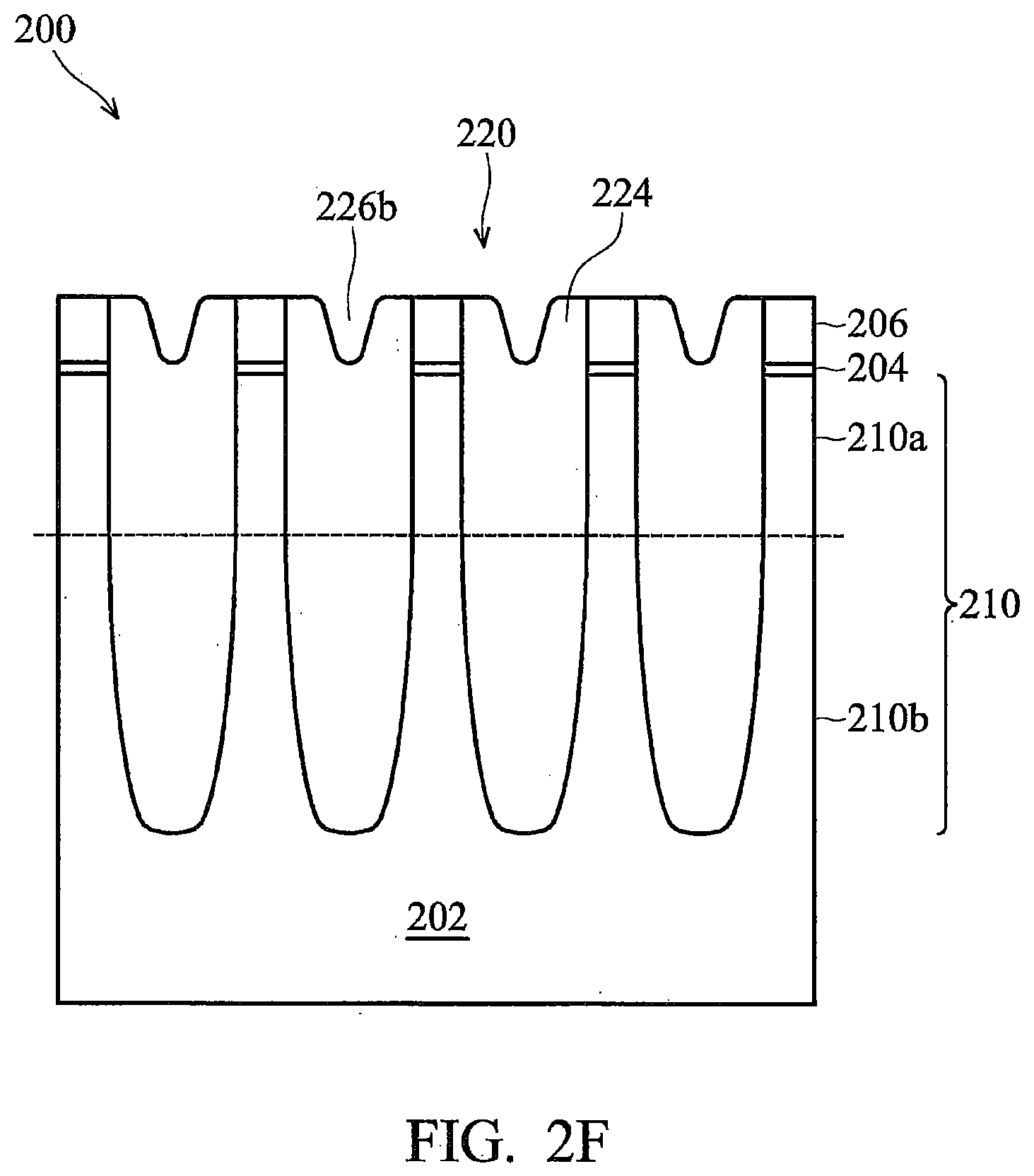
[0025] FIG. 2F shows the substrate 202 of FIG. 2E after a planarization process, such as a chemical mechanical polishing (CMP) process, is performed to remove portions of the dielectric material 224 above the hardmask layer 206 to expose the hardmask layer 206, thereby leaving the dielectric material 224 filling the trenches 222. The hardmask layer 206 also serves as a stop layer for stopping the planarization process on the hardmask layer 206. In some embodiments, a top surface of the dielectric material 224 is or substantially coplanar with the hardmask layer 206. The plurality of the shallow slims 226b of the dielectric material 224 after the planarization process may become even shallower in depth and broader in width than the plurality of shallow slims 226a of the dielectric material 224 before the planarization process.
[0026] Referring to FIG. 2G, after the planarization process, the hardmask layer 206 has been removed by a wet chemical etching process, for example, by dipping the substrate 202 in hot phosphoric acid (H.sub.3PO.sub.4), exposing a top surface of the pad oxide layer 204. Because the wet chemical etching process has higher etch selectivity for nitride than to oxide, the etch process removes the hardmask layer 206 faster than the dielectric material 224. Accordingly, the remaining dielectric material 224 extends over a top surface of the pad oxide layer 204. Subsequent to the hardmask layer 206 removal process, the pad oxide layer 204 has been removed by a wet etching process, for example, by dipping the substrate 202 in hydrofluoric (HF), exposing the top surface of the substrate 202. Since the wet chemical etching process has almost no selectivity for the pad oxide layer 204 and the dielectric material 224, the dielectric material 224 may lose almost the same thickness as the pad oxide layer 204 does. Accordingly, the dielectric material 224 still protrudes over the top surface 210c of each fin structure 210 and each shallow slim recess 226c in the dielectric material 224 almost disappear.
[0027] FIG. 2H shows the substrate 202 of FIG. 2G after a dry etching process, for example, by etching the substrate 202 in a plasma comprising tetrafluormethane (CF4) and trifluormethane (CHF3), is performed to remove upper portions of the dielectric material 224 to expose the upper portion 210a of each fin structure 210. The fin structure could also form part of other devices, such as resistors, capacitors, inductors, fuses, etc. Accordingly, at the end of the etching process, the dielectric material 224 made has almost no recess and serves as the isolation structures 220 between the semiconductor devices. Each isolation structure 220 extends from the substrate surface 202a to a point 224a above the transition location 201d. A third offset distance 216c between the point 224a of the isolation structure 220 and the top surface 210c should be well controlled. If the third offset distance 216c between the point 224a of the isolation structure 220 and the top surface 210c is too small, shallow slims/recesses may still remain on the point 224a of the isolation structure 220. If the third offset distance 216c between the point 224a of the isolation structure 220 and the top surface 210c is too large, short channel effects may degrade device performance. Accordingly, in some embodiments, the third offset distance 216c between the point 224a of the isolation structure 220 and the top surface 210c is preferably in the range of about 15 to 45 nanometers. In some embodiments, the ratio of the third offset distance 216c between the point 224a of the isolation structure 220 and the top surface 210c to the first offset distance 216b between the transition location 210d and the top surface 210c to is preferably from 0.3 to 0.6. FIG. 2I shows a perspective view of the FINFETs 200 fabricated using the steps shown in FIG. 2A-H. Each fin structure 210 extends in a longitudinal direction 210g. As previously described the isolation structure 220 in FIG. 2I has no recesses.
[0028] FIG. 3A-D shows a complete FINFET device 300 having a plurality of isolation structures 220 fabricated using the steps shown in FIG. 2A-H, wherein FIG. 3A shows a perspective view, and wherein FIGS. 3B-D show cross-section views taken along the respective lines of FIG. 3A. Similar features in FIGS. 2 and 3 are numbered the same for the sake of simplicity and clarity.
[0029] Referring to FIG. 3A, the FINFET 300 includes the plurality of fin structures 210 separated by the plurality of isolation structures 220. Each fin structure 210 extends in a longitudinal direction 210g. A gate structure 320 comprising a gate electrode 320a and a gate insulator 320b is disposed over the fin structures 210. FIG. 3A also illustrates the source/drain regions 330a, 330b, 329a and 329b of the FINFET 300.
[0030] FIG. 3B illustrates a cross-sectional view of the FINFET 300 taken along the line b-b of FIG. 3A. Each fin structure 210 extending in a longitudinal direction 210g comprises an upper portion 210a and a lower portion 210b separated at a transition location 210d at where the sidewall of the fin structure 210 at an angle of 85 degrees to the major surface 202a of the substrate 202, the upper portion 210a has sidewalls that are substantially perpendicular to the major surface 202a of the substrate 202 and a top surface 210c, the upper portion 210a comprises a first longitudinal portion 210ga, a second longitudinal portion 210gb, and a third longitudinal portion 210gc disposed between the first and the second longitudinal portions 210ga, 219gb. A channel region 330 is defined within the third longitudinal portion 210gc of the upper portion 210a. A gate structure 320 comprising a gate electrode 320a and a gate insulator 320b may be disposed over the channel region 330. A silicide layer (not shown) may be disposed within the first and the second longitudinal portions 210ga, 219gb form source/drain regions in the FINFET 300. The lower portion 210b under the upper portion 210a has a base 210e and bottom-up tapered sidewalls.
[0031] Referring to the cross sectional view of FIG. 3C taken along the line c-c of FIG. 3A, the gate structure 320 comprises the gate electrode 320a and the gate insulator 320b. The gate electrode 320a is disposed over the gate insulator 320b. If the thickness of the gate insulator 320b is uniform on all the surfaces of the fin structures 210, a triple gate transistor is formed. The channel 330 of the triple gate transistor is disposed under the gate structure 320 and within the top surface 210c and sidewalls of the third longitudinal portion 210gc of the upper portion 210a of the fin structures 210. However, in some embodiments, an additional dielectric layer (not shown) may be formed over the top surface 210c of the third longitudinal portion 210gc of the upper portion 210a before or after forming the gate insulator 310, the channel 330 of the FINFET 300 is formed only along the sidewalls of the third longitudinal portion 210gc, forming a double gate transistor.
[0032] FIG. 3D illustrates a cross-sectional view of the FINFET 300 taken along the line d-d of FIG. 3A. The fin structures 210 disposed between the isolation structures 220 are extending in a longitudinal direction 210g and continuous pieces of the underlying substrate 202. In some embodiments, the fin structures 210 may be separated from the substrate 202 by an insulation layer (not shown). In some embodiments, the first and the second longitudinal portions 210ga, 210gb of the upper portion 210a of the fin structures 210 comprise dopant-rich regions (not shown), and a silicide layer (not shown) may be disposed within the first and the second longitudinal portions 210ga, 210gb forming source/drain regions 329a and 329b in the FINFET 300. In various embodiments, the thickness of the dopant-rich regions is about 0.5 nm to about 10 nm. Then, subsequent processes, including interconnect processing, must be performed after forming the FINFET 300 to complete the IC fabrication.
[0033] While the invention has been described by way of example and in terms of the preferred embodiments, it is to be understood that the invention is not limited to the disclosed embodiments. To the contrary, it is intended to cover various modifications and similar arrangements (as would be apparent to those skilled in the art). Therefore, the scope of the appended claims should be accorded the broadest interpretation so as to encompass all such modifications and similar arrangements. The invention can be used to form or fabricate a fin structure for a FINFET having no isolation recess.
* * * * *
D00000
D00001
D00002
D00003
D00004
D00005
D00006
D00007
D00008
D00009
D00010
D00011
D00012

D00013

D00014

D00015

D00016

XML
uspto.report is an independent third-party trademark research tool that is not affiliated, endorsed, or sponsored by the United States Patent and Trademark Office (USPTO) or any other governmental organization. The information provided by uspto.report is based on publicly available data at the time of writing and is intended for informational purposes only.
While we strive to provide accurate and up-to-date information, we do not guarantee the accuracy, completeness, reliability, or suitability of the information displayed on this site. The use of this site is at your own risk. Any reliance you place on such information is therefore strictly at your own risk.
All official trademark data, including owner information, should be verified by visiting the official USPTO website at www.uspto.gov. This site is not intended to replace professional legal advice and should not be used as a substitute for consulting with a legal professional who is knowledgeable about trademark law.