Method Of Forming An Electrode On A Substrate And A Semiconductor Device Structure Including An Electrode
Mousa; Moataz Bellah ; et al.
U.S. patent application number 16/356394 was filed with the patent office on 2019-10-03 for method of forming an electrode on a substrate and a semiconductor device structure including an electrode. The applicant listed for this patent is ASM IP Holding B.V.. Invention is credited to Peng-Fu Hsu, Ward Johnson, Moataz Bellah Mousa, Petri Raisanen.
| Application Number | 20190304790 16/356394 |
| Document ID | / |
| Family ID | 68055062 |
| Filed Date | 2019-10-03 |


View All Diagrams
| United States Patent Application | 20190304790 |
| Kind Code | A1 |
| Mousa; Moataz Bellah ; et al. | October 3, 2019 |
METHOD OF FORMING AN ELECTRODE ON A SUBSTRATE AND A SEMICONDUCTOR DEVICE STRUCTURE INCLUDING AN ELECTRODE
Abstract
A method of forming an electrode on a substrate is disclosed. The method may include: contacting the substrate with a first vapor phase reactant comprising a titanium tetraiodide (TiI.sub.4) precursor; contacting the substrate with a second vapor phase reactant comprising a nitrogen precursor; and depositing a titanium nitride layer over a surface of the substrate thereby forming the electrode; wherein the titanium nitride layer has an electrical resistivity of less than 400 .mu..OMEGA.-cm. Related semiconductor device structures including a titanium nitride electrode deposited by the methods of the disclosure are also provided.
| Inventors: | Mousa; Moataz Bellah; (Chandler, AZ) ; Hsu; Peng-Fu; (Scottsdale, AZ) ; Johnson; Ward; (Gilbert, AZ) ; Raisanen; Petri; (Gilbert, AZ) | ||||||||||
| Applicant: |
|
||||||||||
|---|---|---|---|---|---|---|---|---|---|---|---|
| Family ID: | 68055062 | ||||||||||
| Appl. No.: | 16/356394 | ||||||||||
| Filed: | March 18, 2019 |
Related U.S. Patent Documents
| Application Number | Filing Date | Patent Number | ||
|---|---|---|---|---|
| 62648832 | Mar 27, 2018 | |||
| Current U.S. Class: | 1/1 |
| Current CPC Class: | H01L 21/02205 20130101; C23C 16/45553 20130101; H01L 21/02186 20130101; H01L 21/32051 20130101; H01L 27/1085 20130101; H01L 21/285 20130101; H01L 21/28562 20130101; H01L 29/4966 20130101; C23C 16/34 20130101; H01L 21/28088 20130101; H01L 21/0228 20130101; H01L 21/823842 20130101; H01L 23/53261 20130101; H01L 21/76877 20130101; H01L 28/60 20130101 |
| International Class: | H01L 21/28 20060101 H01L021/28; H01L 21/02 20060101 H01L021/02; H01L 21/285 20060101 H01L021/285 |
Claims
1. A method of forming an electrode on a substrate, the method comprising: contacting the substrate with a first vapor phase reactant comprising a titanium tetraiodide precursor (TiI.sub.4); contacting the substrate with a second vapor phase reactant comprising a nitrogen precursor; and depositing a titanium nitride layer over a surface of the substrate thereby forming the electrode; wherein the titanium nitride layer has an electrical resistivity of less than 400 .mu..OMEGA.-cm.
2. The method of claim 1, wherein contacting the substrate with the first vapor phase reactant and contacting the substrate with a second vapor phase reactant comprises one deposition cycle of a cyclical deposition process and the method further comprises one or more repeated deposition cycles.
3. The method of claim 2, wherein the cyclical deposition process comprises an atomic layer deposition process, or a cyclical chemical vapor deposition process.
4. The method of claim 1, wherein the nitrogen precursor comprises at least one of ammonia (NH.sub.3), hydrazine (N.sub.2H.sub.4), triazane (N.sub.3H.sub.5), tertbutylhydrazine (C.sub.4H.sub.9N.sub.2H.sub.3), methylhydrazine (CH.sub.3NHNH.sub.2), dimethylhydrazine ((CH.sub.3).sub.2N.sub.2H.sub.2) or a nitrogen containing plasma.
5. The method of claim 1, further comprising heating the substrate to temperature of less than 400.degree. C.
6. The method of claim 1, wherein the titanium nitride layer has an average r.m.s. surface roughness (R.sub.a) of less than 2 Angstroms.
7. The method of claim 1, wherein the titanium nitride layer has a density greater than 5.4 g/cm.sup.3.
8. The method of claim 1, wherein the titanium nitride layer has an electrical resistivity of less than 150 .mu..OMEGA.-cm at a thickness of less than 40 Angstroms.
9. The method of claim 1, wherein the titanium nitride layer comprises a XRD peak intensity ratio <111>:<200>of greater than 2:1.
10. The method of claim 1, wherein the titanium nitride layer is deposited with a step coverage of greater than 95%.
11. The method of claim 1, wherein the substrate comprises a partially fabricated semiconductor device structure including one or more trench structures.
12. The method of claim 11, wherein the titanium nitride layer substantially fills the one or more trench structures.
13. The method of claim 12, further comprising performing a polishing process to planarize and remove excess titanium nitride from an upper exposed surface of the partially fabricated semiconductor device structure, wherein the polishing process results in a planar titanium nitride surface which is substantially free of dishing features.
14. The method of claim 11, wherein the partially fabricated semiconductor device structure comprises a CMOS device structure, or memory device structure.
15. The method of claim 14, wherein the partially fabricated semiconductor device structure comprises a dynamic random access memory (DRAM) device structure.
16. The method of claim 15, wherein the titanium nitride layer comprises a top electrode to the DRAM device.
17. The method of claim 16, wherein the top electrode is deposited at a substrate temperature of less than 300.degree. C.
18. The method of claim 1, wherein the titanium nitride layer has an atomic percentage (at-%) impurity concentration of less than 1%.
19. A semiconductor device structure, the structure comprising: a partially fabricated semiconductor device structure, and a titanium nitride electrode disposed over the partially fabricated semiconductor device structure; wherein the titanium nitride electrode has an electrical resistivity of less than 400 .mu..OMEGA.-cm.
20. The structure of claim 19, wherein the titanium nitride electrode has an average r.m.s. surface roughness (R.sub.a) of less than 2 Angstroms.
21. The structure of claim 19, wherein the titanium nitride electrode has a density greater than 5.4 g/cm.sup.3.
22. The structure of claim 19, wherein the titanium nitride electrode has an electrical resistivity of less than 150 .mu..OMEGA.-cm at a thickness of less than 40 Angstroms.
23. The structure of claim 19, wherein the titanium nitride electrode comprises a XRD peak intensity ratio <111>:<200>greater than 2:1.
24. The structure of claim 19, wherein the partially fabricated semiconductor device structure comprises one or more trench structures and the titanium nitride electrode substantially fills the one or more trench structures.
25. The structure of claim 24, wherein the titanium nitride electrode comprises a planar upper surface substantially free of dishing features.
26. The structure of claim 19, wherein the partially fabricated semiconductor device structure comprises a CMOS device structure, or a memory device.
27. The structure of claim 26, wherein the partially fabricated semiconductor device structure comprises a dynamic random access memory (DRAM) device structure.
28. The structure of claim 27, wherein the titanium nitride electrode comprises a top electrode to the DRAM device structure.
Description
CROSS-REFERENCE TO RELATED PATENT APPLICATION
[0001] The present claims the benefit of U.S. Provisional Patent Application No. 62/648,832, filed on Mar. 27, 2018 and entitled "METHOD OF FORMING AN ELECTRODE ON A SUBSTRATE AND A SEMICONDUCTOR DEVICE STRUCTURE INCLUDING AN ELECTRODE," the disclosure of which is incorporated herein by reference.
FIELD OF INVENTION
[0002] The present disclosure relates generally to methods for forming an electrode on a substrate and particularly methods for a forming a titanium nitride electrode on a partially fabricated semiconductor device structure. The present disclosure also generally relates to a semiconductor device structure and particularly a semiconductor device structure including a titanium nitride electrode.
BACKGROUND OF THE DISCLOSURE
[0003] In the field of semiconductor device fabrication, the trend is towards a reduction in the deposition temperature of metal-containing films, such as, for example, pure metals, metal nitrides, metal carbides, and metal silicides. A reduction in the deposition temperature of metal-containing films may be desirable due to decreasing thermal budget requirements often necessary for the fabrication of state of the art semiconductor device structures, such as, for example, complementary metal-oxide-semiconductor (CMOS) device structures, or memory devices such as dynamic random access memory (DRAM) devices. In particular semiconductor fabrication processes, high temperature deposition of metal-containing films may result in, unwanted thermal diffusion of metal species into adjacent dielectric materials, undesirable diffusion of dopant species in transistor structures, and the formation of unwanted materials.
[0004] However, a reduction in the deposition temperature of metal-containing films, such as, for example, titanium nitride films, may have a detrimental effect on the quality of the deposited film. For example, a reduction in the deposition temperature of a titanium nitride film may have the consequence of a titanium nitride film with reduced crystalline quality and lower density. In the particular case in which the film is electrically conductive, a reduction in deposition temperature may result in an increase in the electrical resistivity of the film as-deposited. Accordingly, methods are desired for depositing a metal-containing film at a reduced deposition temperature whilst maintaining the quality of the as-deposited film.
SUMMARY OF THE DISCLOSURE
[0005] This summary is provided to introduce a selection of concepts in a simplified form. These concepts are described in further detail in the detailed description of example embodiments of the disclosure below. This summary is not intended to identify key features or essential features of the claimed subject matter, nor is it intended to be used to limit the scope of the claimed subject matter.
[0006] In some embodiments of the disclosure, methods for forming an electrode on a substrate are provided. The method may comprise: contacting the substrate with a first vapor phase reactant comprising a titanium tetraiodide (TiI.sub.4); contacting the substrate with a second vapor phase reactant comprising a nitrogen precursor; and depositing a titanium nitride layer over a surface of the substrate thereby forming the electrode; wherein the titanium nitride layer has an electrical resistivity of less than 400 .mu..OMEGA.-cm.
[0007] In some embodiments of the disclosure, semiconductor device structures are provided. The semiconductor device structure may comprise: a partially fabricated semiconductor device structure; and a titanium nitride electrode disposed over the partially fabricated semiconductor device structure; wherein the titanium nitride electrode has an electrical resistivity of less than 400 .mu..OMEGA.-cm.
[0008] For purposes of summarizing the invention and the advantages achieved over the prior art, certain objects and advantages of the invention have been described herein above. Of course, it is to be understood that not necessarily all such objects or advantages may be achieved in accordance with any particular embodiment of the invention. Thus, for example, those skilled in the art will recognize that the invention may be embodied or carried out in a manner that achieves or optimizes one advantage or group of advantages as taught or suggested herein without necessarily achieving other objects or advantages as may be taught or suggested herein.
[0009] All of these embodiments are intended to be within the scope of the invention herein disclosed. These and other embodiments will become readily apparent to those skilled in the art from the following detailed description of certain embodiments having reference to the attached figures, the invention not being limited to any particular embodiment(s) disclosed.
BRIEF DESCRIPTION OF THE DRAWING FIGURES
[0010] While the specification concludes with claims particularly pointing out and distinctly claiming what are regarded as embodiments of the invention, the advantages of embodiments of the disclosure may be more readily ascertained from the description of certain examples of the embodiments of the disclosure when read in conjunction with the accompanying drawings, in which:
[0011] FIG. 1 illustrates a process flow of an exemplary cyclical deposition method according to the embodiments of the disclosure;
[0012] FIG. 2A illustrates a graph demonstrating the relationship between electrical resistivity and substrate temperature during the deposition of titanium nitride films utilizing a titanium tetrachloride (TiCl.sub.4) precursor and utilizing a titanium tetraiodide (TiI.sub.4) precursor.
[0013] FIG. 2B illustrates a graph demonstrating the relationship between electrical resistivity and the thickness of a number of titanium nitride films deposited utilizing a titanium tetraiodide (TiI.sub.4) according to the embodiments of the disclosure;
[0014] FIG. 3A illustrates x-ray diffraction (XRD) data taken from a number of titanium nitride films deposited utilizing a titanium tetraiodide (TiI.sub.4) precursor according to the embodiments of the disclosure;
[0015] FIG. 3B illustrates x-ray diffraction (XRD) data taken from a number of titanium nitride films deposited utilizing a titanium tetrachloride (TiCl.sub.4) precursor according to prior art methods;
[0016] FIG. 4 illustrates a graph demonstrating the relationship between the atomic percentage of impurities within a titanium nitride film and the substrate temperature during the deposition. Percentage impurity concentration data is illustrated for titanium nitride films deposited utilizing the common titanium tetrachloride (TiCl.sub.4) precursor and percentage impurity concentration data is also illustrated for titanium nitride films deposited utilizing the titanium tetraiodide (TiI.sub.4) precursor of the embodiments of the current disclosure;
[0017] FIGS. 5A, 5B and 5C illustrate cross sectional schematic diagrams of prior art semiconductor device structures formed during the fabrication of an electrode;
[0018] FIGS. 6A, 6B and 6C illustrate cross sectional schematic diagrams of partially fabricated semiconductor device structures and the formation of an electrode over such partially fabricated semiconductor device structures according to the embodiments of the disclosure;
[0019] FIG. 7 illustrates a cross sectional schematic diagram of a dynamic random access memory (DRAM) device structure including a titanium nitride electrode deposited according the embodiments of the disclosure; and
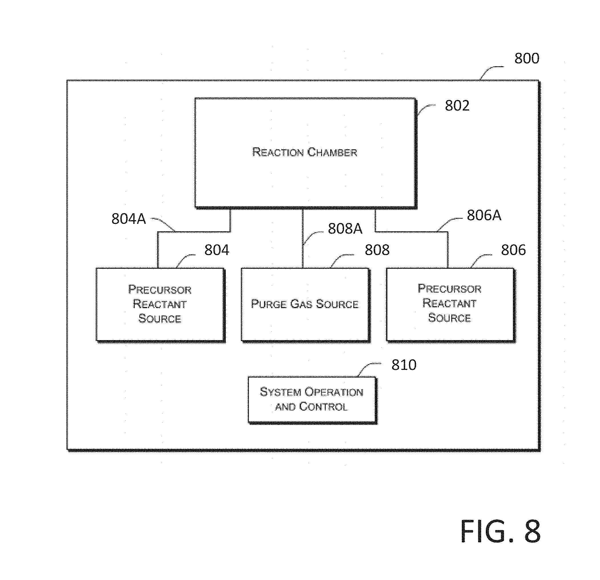
[0020] FIG. 8 illustrates a schematic diagram of a reaction system configured to perform the methods of the disclosure.
DETAILED DESCRIPTION OF EXEMPLARY EMBODIMENTS
[0021] Although certain embodiments and examples are disclosed below, it will be understood by those in the art that the invention extends beyond the specifically disclosed embodiments and/or uses of the invention and obvious modifications and equivalents thereof. Thus, it is intended that the scope of the invention disclosed should not be limited by the particular disclosed embodiments described below.
[0022] The illustrations presented herein are not meant to be actual views of any particular material, structure, or device, but are merely idealized representations that are used to describe embodiments of the disclosure.
[0023] As used herein, the term "cyclic deposition" may refer to the sequential introduction of precursors (reactants) into a reaction chamber to deposit a film over a substrate and includes deposition techniques, such as atomic layer deposition and cyclical chemical vapor deposition.
[0024] As used herein, the term "cyclical chemical vapor deposition" may refer to any process wherein a substrate is sequentially exposed to two or more volatile precursors, which react and/or decompose on a substrate to produce a desired deposition.
[0025] As used herein, the term "substrate" may refer to any underlying material or materials that may be used, or upon which, a device, a circuit or a film may be formed.
[0026] As used herein, the term "atomic layer deposition" (ALD) may refer to a vapor deposition process in which deposition cycles, preferably a plurality of consecutive deposition cycles, are conducted in a process chamber. Typically, during each cycle the precursor is chemisorbed to a deposition surface (e.g., a substrate surface or a previously deposited underlying surface such as material from a previous ALD cycle), forming a monolayer or sub-monolayer that does not readily react with additional precursor (i.e., a self-limiting reaction). Thereafter, if necessary, a reactant (e.g., another precursor or reaction gas) may subsequently be introduced into the process chamber for use in converting the chemisorbed precursor to the desired material on the deposition surface. Typically, this reactant is capable of further reaction with the precursor. Further, purging steps may also be utilized during each cycle to remove excess precursor from the process chamber and/or remove excess reactant and/or reaction byproducts from the process chamber after conversion of the chemisorbed precursor. Further, the term "atomic layer deposition," as used herein, is also meant to include processes designated by related terms such as, "chemical vapor atomic layer deposition", "atomic layer epitaxy" (ALE), molecular beam epitaxy (MBE), gas source MBE, or organometallic MBE, and chemical beam epitaxy when performed with alternating pulses of precursor composition(s), reactive gas, and purge (e.g., inert carrier) gas.
[0027] As used herein, the term "film", "thin film", "layer" and "thin layer" may refer to any continuous or non-continuous structures and material deposited by the methods disclosed herein. For example, "film", "thin film", "layer" and "thin layer" could include 2D materials, nanorods, nanotubes, or nanoparticles or even partial or full molecular layers or partial or full atomic layers or clusters of atoms and/or molecules. "Film", "thin film", "layer" and "thin layer" may comprise material or a layer with pinholes, but still be at least partially continuous.
[0028] As used here, the term "semiconductor structure" may refer to any structure comprising semiconductor materials, including bulk semiconductor materials such as semiconductor substrates (either alone or in assemblies comprising other materials such as metal and insulators thereon), and semiconductor material layers (either alone or in assemblies comprising other materials such as metal and insulators). In addition, the term "semiconductor structure" also includes any supporting structure, including but not limited to, the semiconductor structures describe above. The term "semiconductor structure" may also refer to one or more semiconductor layers or structures which includes active or operable portions of semiconductor devices, as well as semiconductor structures formed during a process that have been fabricated thereon.
[0029] As used herein, the term "partially fabricated semiconductor device structure" may refer to any structure comprising fabricated and partially fabricated active or passive device components intended to be incorporated into one or more semiconductor devices.
[0030] As used herein, the term "electrode" may refer to an electrically conductive member, or at least a portion of an electrically conductive member, configured to pass an electrical current through one or more device structures.
[0031] As used herein, the term "titanium nitride" and "titanium nitride film" may refer to materials comprising titanium species and nitrogen species and may also include ternary titanium nitride films, such as, but not limited to, titanium silicon nitride (TiSiN), titanium oxygen nitride (TiON), or titanium aluminum nitride (TiAlN).
[0032] A number of example materials are given throughout the embodiments of the current disclosure, it should be noted that the chemical formulas given for each of the example materials should not be construed as limiting and that the non-limiting example materials given should not be limited by a given example stoichiometry.
[0033] The present disclosure includes methods that may be utilized to form an electrode on a substrate and in particularly methods for depositing a titanium nitride electrode over a partially fabricated semiconductor device structure utilizing a cyclical deposition process.
[0034] Titanium nitride (TiN) may be useful for many applications in semiconductor device fabrication processes. One or more titanium nitride layers may be utilized as the diffusion barrier layer in an electrode application, wherein the titanium nitride layer may prevent the diffusion of a copper conductor into a surrounding dielectric material. In addition, titanium nitride layers may be utilized as an electrically conductive electrode to memory devices, such as, for example, dynamic random access memory (DRAM) devices.
[0035] A common requisite for the deposition of a titanium nitride film is that the deposition process is extremely conformal. For example, conformal deposition is often required in order to uniformly deposit a titanium nitride film over three-dimensional structures including high aspect ratio features.
[0036] Cyclical deposition processes, such as, atomic layer deposition (ALD) and cyclical chemical vapor deposition (CCVD), sequentially introduce one or more precursors (reactants) into a reaction chamber wherein the precursors react with the surface of the substrate one at a time in a sequential, self-limiting, manner. Cyclical deposition processes have been demonstrated to produce titanium nitride films with excellent conformality with atomic level thickness control.
[0037] In ALD-type processes, a number of precursors may be utilized as the vapor reactant source of titanium for the deposition of a titanium nitride film. One of the most commonly utilized titanium precursors in ALD-type processes is titanium tetrachloride (TiCl.sub.4) due to titanium tetrachloride's advantageous volatility and relatively low cost. However, the deposition of titanium nitride films, utilizing titanium tetrachloride (TiCl.sub.4) as the titanium precursor, may require relatively high temperature depositions, e.g., between approximately 400.degree. C.-600.degree. C., in order to achieve a titanium nitride film with suitable characteristics, such as, for example, a low electrical resistivity. In addition, the titanium tetrachloride (TiCl.sub.4) may liberate chlorine species during the high temperature deposition process which may undesirably etch certain portions of the substrate on which deposition is being performed. Accordingly, methods and related semiconductor device structures are desirable that enable a reduced deposition temperature for titanium nitride films whilst maintaining high quality film characteristics, such as, for example, low electrical resistivity, low impurity concentration, and a high quality crystal structure.
[0038] Therefore, the embodiments of the disclosure may comprise a method of forming an electrode on a substrate. The method may comprise: contacting the substrate with a first vapor phase reactant comprising a titanium tetraiodide (TiI.sub.4) precursor, contacting the substrate with a second vapor phase reactant comprising a nitrogen precursor; and depositing a titanium nitride layer over a surface of the substrate thereby forming the electrode; wherein the titanium nitride layer has an electrical resistivity of less than less than 400.mu..OMEGA.-cm.
[0039] In some embodiments of the disclosure, a titanium nitride layer (or film) may be deposited by a cyclical deposition process utilizing titanium tetraiodide (TiI.sub.4) as the titanium precursor. A non-limiting example embodiment of a cyclical deposition process may include atomic layer deposition (ALD), wherein ALD is based on typically self-limiting reactions, whereby sequential and alternating pulses of reactants are used to deposit about one atomic (or molecular) monolayer of material per deposition cycle. The deposition conditions and precursors are typically selected to provide self-saturating reactions, such that an adsorbed layer of one reactant leaves a surface termination that is non-reactive with the gas phase reactants of the same reactant. The substrate is subsequently contacted with a different reactant that reacts with the previous termination to enable continued deposition. Thus, each cycle of alternated pulses typically leaves no more than about one monolayer of the desired material. However, as mentioned above, the skilled artisan will recognize that in one or more ALD cycles more than one monolayer of material may be deposited, for example if some gas phase reactions occur despite the alternating nature of the process.
[0040] In an ALD-type process for depositing a titanium nitride film, one deposition cycle may comprise, contacting the substrate to a first reactant, removing any unreacted first reactant and reaction byproducts from the reaction space, and contacting the substrate to a second reactant, followed by a second removal step. The first reactant may comprise a titanium tetraiodide precursor ("the titanium precursor") and the second reactant may comprise a nitrogen precursor ("the nitrogen precursor").
[0041] Precursors may be separated by inert gases, such as argon (Ar) or nitrogen (N.sub.2), to prevent gas-phase reactions between reactants and enable self-saturating surface reactions. In some embodiments, however, the substrate may be moved to separately contact a first vapor phase reactant and a second vapor phase reactant. Because the reactions self-saturate, strict temperature control of the substrates and precise dosage control of the precursors may not be required. However, the substrate temperature is preferably such that an incident gas species does not condense into monolayers nor decompose on the surface. Surplus chemicals and reaction byproducts, if any, are removed from the substrate surface, such as by purging the reaction space or by moving the substrate, before the substrate is contacted with the next reactive chemical. Undesired gaseous molecules can be effectively expelled from a reaction space with the help of an inert purging gas. A vacuum pump may be used to assist in the purging.
[0042] Reactors capable of being used to deposit titanium nitride films can be used for the deposition. Such reactors include ALD reactors, as well as CVD reactors equipped with appropriate equipment and means for providing the precursors. According to some embodiments, a showerhead reactor may be used. According to some embodiments, cross-flow, batch, minibatch, or spatial ALD reactors may be used. In at least one embodiment, a vertical furnace reactor may be used.
[0043] In some embodiments, the wafers rotate during processing. In other embodiments, the batch reactor comprises a minibatch reactor configured to accommodate 10 or fewer wafers, 8 or fewer wafers, 6 or fewer wafers, 4 or fewer wafers, or 2 or fewer wafers. In some embodiments in which a batch reactor is used, wafer-to-wafer non-uniformity is less than 3% (lsigma), less than 2%, less than 1% or even less than 0.5%.
[0044] The deposition processes described herein can optionally be carried out in a reactor or a reaction chamber connected to a cluster tool. In a cluster tool, because each reaction chamber is dedicated to one type of process, the temperature of the reaction chamber in each module can be kept constant, which improves the throughput compared to a reactor in which the substrate is heated up to the process temperature before each run. Additionally, in a cluster tool it is possible to reduce the time to pump the reaction chamber to the desired process pressure levels between substrates. In some embodiments of the disclosure, the deposition process may be performed in a cluster tool comprising multiple reaction chambers, wherein each individual reaction chamber may be utilized to expose the substrate to an individual precursor gas and the substrate may be transferred between different reaction chambers for exposure to multiple precursors gases, the transfer of the substrate being performed under a controlled ambient to prevent oxidation/contamination of the substrate. In some embodiments of the disclosure, the deposition process may be performed in a cluster tool comprising multiple reaction chambers, wherein each individual reaction chamber may be configured to heat the substrate to a different deposition temperature.
[0045] A stand-alone reactor can be equipped with a load-lock. In that case, it is not necessary to cool down the reaction space between each run. In some embodiments a deposition process for depositing a titanium nitride film may comprise a plurality of deposition cycles, for example ALD cycles, or cyclical CVD cycles.
[0046] In some embodiments, the cyclical deposition processes are used to form titanium nitride films on a substrate and the cyclical deposition process may be an ALD type process. In some embodiments the cyclical deposition may be a hybrid ALD/CVD or cyclical CVD process. For example, in some embodiments, the growth rate of the ALD process may be low compared with a CVD process. One approach to increase the growth rate may be that of operating at a higher substrate temperature than that typically employed in an ALD process, resulting in a chemical vapor deposition process, but still taking advantage of the sequential introduction of precursors, such a process may be referred to as cyclical CVD.
[0047] According to some embodiments of the disclosure, ALD processes may be used to deposit a titanium nitride film on a substrate, such as a partially fabricated semiconductor device structure. In some embodiments of the disclosure, each ALD cycle comprises two distinct deposition steps or phases. In a first phase of the deposition cycle ("the metal phase"), the substrate surface on which deposition is desired is contacted with a first vapor phase reactant comprising a metal precursor which chemisorbs onto the substrate surface, forming no more than about one monolayer of reactant species on the surface of the substrate. In a second phase of the deposition ("the nitrogen phase"), the substrate surface on which deposition is desired is contacted with a second vapor phase reactant comprising a nitrogen precursor, wherein the nitrogen precursor may react with titanium species on a surface of the substrate to form a titanium nitride layer.
[0048] In some embodiments of the disclosure, the first vapor phase reactant may comprise a metal containing precursor, also referred to here as the "metal compound". In some embodiments, the first vapor phase reactant may comprise a titanium tetraiodide (TiI.sub.4) precursor.
[0049] In some embodiments of the disclosure, contacting the substrate with a first vapor phase reactant comprising a titanium tetraiodide (TiI.sub.4) precursor may comprise exposing, i.e., contacting, the substrate to the titanium tetraiodide (TiI.sub.4) precursor for a time period of between about 0.01 seconds and about 60 seconds, or between about 0.05 seconds and about 10 seconds, or between about 0.1 seconds and about 5.0 seconds. In addition, during the contacting of the substrate with the titanium tetraiodide (TiI.sub.4) precursor, the flow rate of the titanium tetraiodide (TiI.sub.4) precursor may be less than 2000 sccm, or less than 500 sccm, or even less than 100 sccm. In addition, during the contacting of the substrate with the titanium tetraiodide (TiI.sub.4) precursor over the substrate the flow rate of the titanium tetraiodide (TiI.sub.4) precursor may from about 1 to 2000 sccm, from about 5 to 1000 sccm, or from about 10 to about 500 sccm.
[0050] Excess titanium tetraiodide (TiI.sub.4) precursor and reaction byproducts (if any) may be removed from the surface, e.g., by pumping with an inert gas. For example, in some embodiments of the disclosure, the methods may comprise a purge cycle wherein the substrate surface is purged for a time period of less than approximately 2.0 seconds. Excess metal precursor and any reaction byproducts may be removed with the aid of a vacuum, generated by a pumping system, in fluid communication with the reaction chamber.
[0051] In a second phase of the deposition cycle ("the nitrogen phase") the substrate may be contacted with a second vapor phase reactant comprising a nitrogen precursor. In some embodiments of the disclosure, the nitrogen precursor may comprise at least one of ammonia (NH.sub.3), hydrazine (N2H4), triazane (N.sub.3H.sub.5), tertbutylhydrazine (C.sub.4H.sub.9N.sub.2H.sub.3), methylhydrazine (CH.sub.3NHNH.sub.2), dimethylhydrazine ((CH3).sub.2N.sub.2H.sub.2), or a nitrogen plasma.
[0052] In some embodiments of the disclosure, contacting, i.e., exposing, the substrate to the nitrogen precursor may comprise contacting of the nitrogen precursor to the substrate for a time period of between 0.1 seconds and 2.0 seconds, or from about 0.01 seconds to about 10 seconds, or less than about 20 seconds, or less than about 10 seconds, or even less than about 5 seconds. During the contacting of the nitrogen precursor to the substrate, the flow rate of the nitrogen precursor may be less than 30 slm, or less than 20 slm, or less than 10 slm, or less than 5 slm, or even less than 1 slm.
[0053] The second vapor phase reactant comprising a nitrogen precursor may react with titanium species left on the substrate. In some embodiments, the second phase precursor may comprise ammonia (NH.sub.3) and the reaction with titanium species left on the substrate may deposit a titanium nitride layer.
[0054] Excess second vapor phase reactant (e.g., the nitrogen precursor) and reaction byproducts, if any, may be removed from the substrate surface, for example, by a purging gas pulse and/or vacuum generated by a pumping system. Purging gas is preferably any inert gas, such as, without limitation, argon (Ar), nitrogen (N.sub.2), or helium (He). A phase is generally considered to immediately follow another phase if a purge (i.e., purging gas pulse) or other reactant removal step intervenes.
[0055] A deposition cycle in which the substrate is alternatively contacted with the first vapor phase reactant (i.e., the titanium tetraiodide precursor) and the second vapor phase reactant (i.e., the nitrogen precursor) may be repeated one or more times until a desired thickness of a titanium nitride film is deposited. It should be appreciated that in some embodiments of the disclosure, the order of the contacting of the substrate with the first vapor phase reactant and the second vapor phase reactant may be such that the substrate is first contacted with the second vapor phase reactant followed by the first vapor phase reactant. In addition, in some embodiments, the cyclical deposition process may comprise contacting the substrate with the first vapor phase reactant (i.e., the titanium precursor) one or more times prior to contacting the substrate with the second vapor phase reactant (i.e., the nitrogen precursor) one or more times and similarly may alternatively comprise contacting the substrate with the second vapor phase reactant one or more times prior to contacting the substrate with the first vapor phase reactant one or more times.
[0056] In addition, some embodiments of the disclosure may comprise non-plasma reactants, e.g., the first and second vapor phase reactants are substantially free of ionized reactive species. In some embodiments, the first and second vapor phase reactants are substantially free of ionized reactive species, excited species, or radical species. For example, both the first vapor phase reactant and the second vapor phase reactant may comprise non-plasma reactants to prevent ionization damage to the underlying substrate and the associated defects thereby created. The use of non-plasma reactants may be especially useful when the underlying substrate contains fragile fabricated, or least partially fabricated, semiconductor device structures as the high energy plasma species may damage and/or deteriorate device performance characteristics.
[0057] The cyclical deposition processes described herein, utilizing a titanium tetraiodide (TiI.sub.4) precursor and a nitrogen precursor to deposit a titanium nitride layer, may be performed in an ALD or CVD deposition system with a heated substrate. For example, in some embodiments, methods may comprise heating the substrate to temperature of between approximately 300.degree. C. and approximately 500.degree. C., or even heating the substrate to a temperature of between approximately 200.degree. C. and approximately 500.degree. C. Of course, the appropriate temperature window for any given cyclical deposition process, such as, for an ALD reaction, will depend upon the surface termination and reactant species involved. Here, the temperature varies depending on the precursors being used and is generally at or below about 700.degree. C. In some embodiments, the deposition temperature is generally at or above about 100.degree. C. for vapor deposition processes, in some embodiments the deposition temperature is between about 100.degree. C. and about 250.degree. C., and in some embodiments the deposition temperature is between about 120.degree. C. and about 200.degree. C. In some embodiments the deposition temperature is less than about 500.degree. C., or less than below about 400.degree. C., or less than about 350.degree. C., or below about 300.degree. C. In some instances the deposition temperature can be below about 200.degree. C., or below about 150.degree. C., or even below about 100.degree. C. In some instances the deposition temperature can be above about 20.degree. C., or above about 50.degree. C., or even above about 75.degree. C. In some embodiments of the disclosure, the deposition temperature i.e., the temperature of the substrate during deposition, is approximately 400.degree. C.
[0058] In some embodiments, the growth rate of the titanium nitride film is from about 0.005 .ANG./cycle to about 5 .ANG./cycle, or from about 0.01 .ANG./cycle to about 2.0 .ANG./cycle. In some embodiments, the growth rate of the titanium nitride film is more than about 0.05 .ANG./cycle, or more than about 0.1 .ANG./cycle, or more than about 0.15 .ANG./cycle, or more than about 0.20 .ANG./cycle, or more than about 0.25 .ANG./cycle, or even more than about 0.3 .ANG./cycle. In some embodiments, the growth rate of the titanium nitride film is less than about 2.0 .ANG./cycle, or less than about 1.0 .ANG./cycle, or less than about 0.75 .ANG./cycle, or less than about 0.5 .ANG./cycle, or even less than about 0.2 .ANG./cycle. In some embodiments of the disclosure, the growth rate of the titanium nitride film may be approximately 0.4 .ANG./cycle for a deposition temperature of approximately 400.degree. C. In some embodiments of the disclosure, the growth rate of the titanium nitride film may be approximately 0.20 .ANG./cycle for a deposition temperature of approximately 300.degree. C.
[0059] The embodiments of the disclosure may comprise a cyclical deposition which may be illustrated in more detail by exemplary cyclical deposition method 100 of FIG. 1. The method 100 may begin with a process block 110 which comprises, providing at least one substrate into a reaction chamber and heating the substrate to the deposition temperature. For example, the substrate may comprise one or more partially fabricated semiconductor device structures, the reaction chamber may comprise an atomic layer deposition reaction chamber, and the substrate may be heated to a deposition temperature of approximately less than 500.degree. C. In addition, the pressure within the reaction chamber may be controlled to provide a reduced atmosphere in the reaction chamber. For example, the pressure within the reaction chamber during the cyclical deposition process may be less than 5 Torr, or less than 3 Ton, or even less than 1 Torr.
[0060] The method 100 may continue with a process block 120 which comprises, contacting the substrate with a titanium tetraiodide (TiI.sub.4) precursor, for example, the substrate may be contacted with the titanium tetraiodide (TiI.sub.4) for a time period of approximately 2 second. Upon contacting the substrate with the titanium tetraiodide (TiI.sub.4) precursor, excess titanium tetraiodide (TiI.sub.4) precursor and any reaction byproducts may be removed from the reaction chamber by a purge/pump process. The method 100 may continue with a process block 130 which comprises, contacting the substrate with a nitrogen precursor, such as, for example, ammonia (NH.sub.3) for a time period of approximately 2 seconds. Upon contacting the substrate with the nitrogen precursor, the excess nitrogen precursor and any reaction byproducts may be removed from the reaction chamber by a purge/pump process.
[0061] The exemplary cyclical deposition method 100 wherein the substrate is alternatively and sequentially contacted with the titanium tetraiodide (TiI.sub.4) precursor (process block 120) and contacted with the nitrogen precursor (process block 130) may constitute one deposition cycle. In some embodiments of the disclosure, the method of depositing a titanium nitride film may comprise repeating the deposition cycle one or more times. For example, the method 100 may continue with a decision gate 140 which determines if the cyclical deposition method 100 continues or exits via a process block 150. The decision gate 140 is determined based on the thickness of the titanium nitride film deposited, for example, if the thickness of the titanium nitride film is insufficient for the desired device structure, then the method 100 may return to the process block 120 and the processes of contacting the substrate with the titanium tetraiodide (TiI.sub.4) precursor and contacting the substrate with the nitrogen precursor may be repeated one or more times. Once the titanium nitride film has been deposited to a desired thickness the method may exit via the process block 150 and the titanium nitride film and the underlying semiconductor structure may be subjected to additional processes to form one or device structures.
[0062] Films, or layers, comprising titanium nitride deposited according to some of the embodiments described herein may be continuous thin films. In some embodiments the thin films comprising a titanium nitride film deposited according to some of the embodiments described herein may be continuous at a thickness below approximately 100 nanometers, or below approximately 60 nanometers, or below approximately 50 nanometers, or below approximately 40 nanometers, or below approximately 30 nanometers, or below approximately 25 nanometers, or below approximately 20 nanometers, or below approximately 15 nanometers, or below approximately 10 nanometers, or below approximately 5 nanometers, or below approximately 2 nanometers, or lower. The continuity referred to herein can be physical continuity or electrical continuity. In some embodiments, the thickness at which a film may be physically continuous may not be the same as the thickness at which a film is electrically continuous, and the thickness at which a film may be electrically continuous may not be the same as the thickness at which a film is physically continuous.
[0063] In some embodiments, a titanium nitride film deposited according to some of the embodiments described herein may have a thickness from about 20 nanometers to about 100 nanometers. In some embodiments, a titanium nitride film deposited according to some of the embodiments described herein may have a thickness from about 20 nanometers to about 60 nanometers. In some embodiments, a titanium nitride film deposited according to some of the embodiments described herein may have a thickness from about 1 nanometer to about 10 nanometers. In some embodiments, a titanium nitride film deposited according to some of the embodiments described herein may have a thickness greater than about 20 nanometers, or greater than about 30 nanometers, or greater than about 40 nanometers, or greater than about 50 nanometers, or greater than about 60 nanometers, or greater than about 100 nanometers, or greater than about 250 nanometers, or greater than about 500 nanometers, or greater. In some embodiments a titanium nitride film deposited according to some of the embodiments described herein may have a thickness of less than about 50 nanometers, or less than about 30 nanometers, or less than about 20 nanometers, or less than about 15 nanometers, or less than about 10 nanometers, or less than about 5 nanometers, or less than about 3 nanometers, or less than about 2 nanometers, or even less than about 1 nanometer.
[0064] In some embodiments of the disclosure, the titanium nitride film may be deposited on a three-dimensional structure, e.g., a non-planar substrate comprising high aspect ratio features. In some embodiments, the step coverage of the titanium nitride film may be equal to or greater than about 50%, or greater than about 80%, or greater than about 90%, or greater than about 95%, or greater than about 98%, or greater than about 99%, or greater in structures having aspect ratios (height/width) of more than about 2, more than about 5, more than about 10, more than about 25, more than about 50, or even more than about 100.
[0065] The exemplary cyclical deposition methods described herein may be utilized to deposit titanium nitride films with reduced electrical resistivity when compared to prior art deposition methods. In more detail, FIG. 2A illustrates a graph demonstrating the relationship between electrical resistivity and substrate temperature during the cyclical deposition of a number of titanium nitride films deposited employing a prior art method utilizing a titanium tetrachloride (TiCl.sub.4) precursor and alternatively utilizing the embodiments of the current disclosure, i.e., a cyclical deposition process utilizing a titanium tetraiodide (TiI.sub.4) precursor. It should be noted that all the data present in FIG. 2A is collected from titanium nitride films with a thickness of approximately 100 Angstroms. The data represented by line 200 illustrates the electrical resistivity of a number of titanium nitride films deposited at various substrate temperatures utilizing a titanium tetrachloride (TiCl.sub.4) precursor. The data represented by line 202 illustrates the electrical resistivity of a number a titanium nitride films deposited at various substrate temperatures utilizing a titanium tetraiodide (TiI.sub.4) precursor according to the embodiments of the current disclosure. Examination of the electrical resistivity data in FIG. 2A clearly demonstrates that for a given substrate temperature the electrical resistivity (.mu..OMEGA.-cm) of the titanium nitride films deposited utilizing a titanium tetraiodide (TiI.sub.4) precursor is substantially lower than the electrical resistivity (.mu..OMEGA.-cm) of the titanium nitride films deposited utilizing a titanium tetrachloride (TiCl.sub.4) precursor. For example, in some embodiments of the disclosure, a titanium nitride layer may be deposited utilizing a titanium tetraiodide (TiI.sub.4) precursor at a substrate temperature of less than 350.degree. C., wherein the titanium nitride layer has an electrical resistivity of less than 400 .mu..OMEGA.-cm. In some embodiments of the disclosure, a titanium nitride layer may be deposited utilizing a titanium tetraiodide (TiI.sub.4) precursor at a substrate temperature of less than 400.degree. C., wherein the titanium nitride layer has an electrical resistivity of less than 200 .mu..OMEGA.-cm. In some embodiments of the disclosure, a titanium nitride layer may be deposited utilizing a titanium tetraiodide (TiI.sub.4) precursor at a substrate temperature of less than 450.degree. C., wherein the titanium nitride layer has an electrical resistivity of less than 125 .mu..OMEGA.-cm.
[0066] Further data demonstrating the electrical resistivity of titanium nitride films deposited according to the embodiments of the disclosure are shown in FIG. 2B which comprises, a graph demonstrating the relationship between electrical resistivity (.mu..OMEGA.-cm) and the film thickness of a number of titanium nitride films deposited according to the embodiments of the disclosure. It should be noted that all the titanium nitride films utilized to produce the data in FIG. 2B were deposited utilizing a titanium tetraiodide (TiI.sub.4) precursor at a substrate temperature of 450.degree. C. In some embodiments, a titanium nitride film may be deposited to a thickness of less than 100 Angstroms with an electrical resistivity of less than 100 .mu..OMEGA.-cm. In some embodiments, a titanium nitride film may be deposited to a thickness of less than 50 Angstroms with an electrical resistivity of less than 200 .mu..OMEGA.-cm. In some embodiments, a titanium nitride film may be deposited to a thickness of less than 40 Angstroms with an electrical resistivity of less than 250 .mu..OMEGA.-cm. In additional embodiments of the disclosure, a titanium nitride film may be deposited to a thickness of less than 40 Angstroms with an electrical resistivity of less than 150 .mu..OMEGA.-cm.
[0067] The exemplary cyclical deposition methods disclosed herein may also deposit titanium nitride films with improved average r.m.s. surface roughness. For example, in some embodiments, the titanium nitride films may have an average r.m.s. surface roughness (R.sub.a) (as-deposited) of less than 4 Angstroms, or less than 2 Angstroms, or even less than 0.5 Angstroms. The average r.m.s. surface roughness (R.sub.a) of the as-deposited titanium nitride films may be determined employing atomic force microscopy, e.g., by a scanning a surface area of approximately 100 .mu.m .times.100 .mu.m.
[0068] The exemplary cyclical deposition methods disclosed herein may also deposit titanium nitride films with an increased density compared with prior deposition methods. For example, in some embodiments of the disclosure, the titanium nitride films may have a density greater than 4.8 g/cm.sup.3, or greater than 5.0 g/cm.sup.3, or even greater than 5.3 g/cm.sup.3. In some embodiments, the titanium nitride film deposited according to the embodiments of the current disclosure may have a density of equal to or greater than approximately 4.85 g/cm.sup.3 when deposited at a deposition temperature of less than approximately 300.degree. C. In some embodiments, the titanium nitride film deposited according to the embodiments of the current disclosure may have a density of equal to or greater than approximately 5.25 g/cm.sup.3 when deposited at a deposition temperature of less than approximately 400.degree. C.
[0069] The exemplary cyclical deposition methods disclosed herein may also deposit titanium nitride films with an improved crystalline structure. In more detail, FIG. 3A illustrates a graph showing the 2 theta x-ray diffraction (XRD) scans of a number of titanium nitride films deposited according to the embodiments of the disclosure. For example, the data represented by line 300 was measured from a titanium nitride film deposited utilizing titanium tetraiodide (TiI.sub.4) as the titanium precursor at a substrate temperature of 300.degree. C. to a thickness of approximately 180 Angstroms, and the data represented by line 302 was measured from a titanium nitride film deposited utilizing titanium tetraiodide (TiI.sub.4) as the titanium precursor at a substrate temperature of 400.degree. C. to a thickness of approximately 180 Angstroms. Both sets of XRD data clearly show peaks at the position denoted by the label 304 and the position denoted by the label 306, wherein the peak denoted by label 304 corresponds to a <111>crystal structure and the peak denoted by label 306 corresponds to a <200>crystal structure. An indication of the crystal quality of the titanium nitride films deposited according to the embodiments of the current disclosure may be ascertained by the width of the peaks in the XRD data and in particular the crystalline quality may ascertained by examination of the full-width-half-maximum (FWHM) value of the <111>crystal structure peak denoted by label 304. For example, in some embodiments of the disclosure the titanium nitride may be deposited utilizing a titanium tetraiodide (TiI.sub.4) precursor at a substrate temperature of less than or equal to 400.degree. C. and the resulting titanium nitride film may comprise a <111>crystal structure as illustrated by peak 304 in the XRD data of FIG. 3A, the peak 304 in the XRD having a FWHM of less than 1.degree.. In some embodiments of the disclosure, the titanium nitride may be deposited utilizing a titanium tetraiodide (TiI.sub.4) precursor at a substrate temperature of less than or equal to 300.degree. C. and the resulting titanium film may comprise a <111>crystal structure as illustrated by peak 304 in the XRD data of FIG. 3A, the peak 304 in the XRD having a FWHM of less than 1.degree..
[0070] A further indication of the crystalline quality of the titanium nitride films deposited according to the embodiments of the disclosure may be established by examining the relative intensities of the XRD peaks 304 and 306 in FIG. 3A. For example, the XRD data represented by lines 300 and 302 are both dominated by XRD peak 304, corresponding to a <111>crystal structure, with a lesser XRD peak 306, corresponding to a <200>crystal structure. The crystalline quality of the titanium nitride films deposited according to the embodiments of the disclosure may be represented by the XRD intensity ratio of the <111>crystal structure (XRD peak 304) to the <200>crystal structure (XRD peak 306). For example, in some embodiments the XRD intensity ratio <111>:<200>may be greater than 1:1, or greater than 2:1, or greater than 3:1, or greater than 4:1, or even greater than 5:1. In some embodiments, the XRD intensity ratio <111>:<200>may be greater than 2:1, or greater than 2.5:1, or even greater than 3:1, for a titanium nitride deposited utilizing a titanium tetraiodide precursor at a deposition temperature equal to or less than approximately 400.degree. C. In some embodiments, the XRD intensity ratio <111>:<200>may be greater than 2:1, greater than 2.5:1, or even greater than 3:1, for a titanium nitride deposited utilizing a titanium tetraiodide precursor at a deposition temperature equal to or less than approximately 300.degree. C. In addition, in some embodiments, the XRD intensity ratio <111>:<200>for titanium nitride film deposited utilizing a titanium tetraiodide precursor may be substantially temperature independent for deposition temperatures between approximately 300.degree. C. and approximately 400.degree. C.
[0071] In contrast to the cyclical deposition methods disclosed herein, i.e., a cyclical deposition process comprising a titanium tetraiodide precursor, FIG. 3B illustrates the 2 theta x-ray diffraction (XRD) scans of a number of titanium nitride films deposited according to prior art methods utilizing titanium tetrachloride (TiCl.sub.4) as the titanium precursor. The XRD peaks labelled as 308A, 308B, and 308C denote titanium nitride films comprising a <111>crystal structure, deposited at a substrate temperature of approximately 400.degree. C. (XRD peak 308A), deposited at a substrate temperature of approximately 350.degree. C. (XRD peak 308B), and deposited at a substrate temperature of approximately 300.degree. C. (XRD peak 308C). In addition, the XRD peaks labelled as 310A, 310B, and 310C denote titanium nitride films comprising a <200>crystal structure, deposited at a substrate temperature of approximately 400.degree. C. (XRD peak 310A), deposited at a substrate temperature of approximately 350.degree. C. (XRD peak 310B), and deposited at a substrate temperature of approximately 300.degree. C. (XRD peak 310C).
[0072] As previously described herein, an indication of the crystalline quality of a titanium nitride film may be given by the XRD peak intensity ratio of the <111>crystal structure to the <200>crystal structure. Examination of FIG. 3B illustrates that as the deposition temperature of the titanium nitride films deposited utilizing titanium tetrachloride reduces from approximately 400.degree. C., down to approximately 350.degree. C., and further down to approximately 300.degree. C., the XRD peak intensity ratio <111>:<200>correspondingly changes from approximately 2:1 at a deposition temperature of approximately 400.degree. C., to approximately 1:1.25 at a deposition temperature of approximately 350.degree. C., to approximately 1:2 at a deposition temperature of approximately 300.degree. C. The variation observed in the XRD peak intensity ratio <111>:<200>for titanium nitride films deposited utilized titanium tetrachloride is in sharp contrast to that seen in FIG. 3A for titanium nitride films deposited utilizing titanium tetraiodide, wherein the XRD peak intensity ratio <111>:<200>is significantly higher and less deposition temperature dependent.
[0073] In some embodiments of the disclosure, the metal precursor may comprise a titanium tetraiodide (TiI.sub.4) precursor and the nitrogen precursor may comprise ammonia (NH.sub.3) and film deposited by the methods of the disclosure may comprise a titanium nitride film. In some embodiments, the titanium nitride film may comprise a titanium atomic %, i.e., a titanium content, of greater than 48 atomic %, or greater than 49 atomic %, or even greater than 50 atomic %. In the embodiments outlined herein, the atomic concentration of an element may be determined utilizing Rutherford backscattering (RBS).
[0074] The exemplary cyclical deposition methods disclosed herein may also deposit titanium nitride films with an improved impurity concentration compared with titanium nitride films deposited via prior art methods. In more detail, FIG. 4 illustrates a graph demonstrating the relationship between the atomic percentage (at-%) of impurities within a number of titanium nitride films and the substrate temperature during the deposition. Percentage impurity concentration data is illustrated for titanium nitride films deposited utilizing the common titanium tetrachloride (TiCl.sub.4) precursor (as represented by the circular data markers) and percentage impurity concentration data is also illustrated for titanium nitride films deposited utilizing the titanium tetraiodide (TiI.sub.4) precursor (as represented by the crossed data markers) of the embodiments of the current disclosure. It should be noted that the impurity concentration data represented in FIG. 4 was obtained utilizing x-ray photoelectron spectroscopy (XPS). Examination of the impurity concentration data illustrated in FIG. 4, clearly demonstrates that for a given deposition temperature (.degree. C.) the titanium nitride films deposited utilizing the titanium tetraiodide (TiI.sub.4) precursor have a lower atomic percentage (at-%) impurity concentration compared with titanium nitride films deposited utilizing a titanium tetrachloride (TiCl.sub.4) precursor. For example, for a titanium nitride film deposited utilizing a titanium tetraiodide (TiI.sub.4) precursor at a substrate temperature of less than or equal to 250.degree. C., the titanium nitride film has an atomic percentage (at-%) impurity concentration of less than 3%. In some embodiments, a titanium nitride film deposited utilizing a titanium tetraiodide (TiI.sub.4) precursor at a substrate temperature of less than or equal to 300.degree. C., the titanium nitride film has an atomic percentage (at-%) impurity concentration of less than 2%. In some embodiments, a titanium nitride film deposited utilizing a titanium tetraiodide (TiI.sub.4) precursor at a substrate temperature of less than or equal to 350.degree. C., the titanium nitride film has an atomic percentage (at-%) impurity concentration of less than 1%. In some embodiments, a titanium nitride film deposited utilizing a titanium tetraiodide (TiI.sub.4) precursor at a substrate temperature of less than or equal to 400.degree. C., the titanium nitride film has an atomic percentage (at-%) impurity concentration of less than 0.5%. In some embodiments, the impurities within the titanium nitride films deposited according to the current disclosure may include, but are not limited, to oxygen (O), iodine (I), and hydrogen (H).
[0075] In some embodiments of the disclosure the deposition methods disclosed herein may be utilized to deposit further forms of titanium nitride, such as, for example, a ternary titanium nitride. Therefore, the methods disclosed herein may be utilized to deposit a ternary titanium nitride, such as, for example, a titanium silicon nitride (TiSiN), a titanium oxygen nitride (TiON), or a titanium aluminum nitride (TiAlN). As a non-limiting example, a deposition cycle for depositing a ternary titanium nitride may comprise, contacting the substrate with a first vapor phase reactant comprising a titanium precursor, contacting the substrate with a second vapor phase reactant comprising a nitrogen precursor, and contacting the substrate with a third vapor phase reactant comprising at least one of a silicon precursor, an oxygen precursor, or an aluminum precursor.
[0076] In some embodiments of the disclosure, the first vapor phase reactant may comprise a titanium tetraiodide (TiI.sub.4). In some embodiments of the disclosure, the second vapor phase reactant may comprise a nitrogen precursor, such as, for example, at least one of ammonia (NH.sub.3), hydrazine (N.sub.2H.sub.4), triazane (N.sub.3H.sub.5), tertbutylhydrazine (C.sub.4H.sub.9N.sub.2H.sub.3), methylhydrazine (CH.sub.3NHNH.sub.2), dimethylhydrazine ((CH.sub.3)2N.sub.2H.sub.2), or a nitrogen plasma.
[0077] In some embodiments, the third vapor phase reactant may comprise a silicon precursor and the ternary titanium nitride deposited may comprise a titanium silicon nitride (TiSiN). In some embodiments, the silicon precursor may comprise at least one of silane (SiH.sub.4), disilane (Si.sub.2H.sub.6), trisilane (Si.sub.3H.sub.8), chlorosilane (SiH.sub.3Cl), dichlorosilane (SiH.sub.2Cl.sub.2), silicon tetrachloride (SiCl.sub.4), silicon tetraiodide (SiI.sub.4), hexachlorodisilane (Si.sub.2Cl.sub.6), trichlorosilane (SiHCl.sub.3), or methyl silane (SiCH.sub.6).
[0078] In some embodiments of the disclosure, the third vapor phase reactant may comprise an oxygen precursor and the ternary titanium nitride deposited may comprise a titanium oxygen nitride (TiON). In some embodiments, the oxygen precursor may comprise at least one of ozone (O.sub.3), an oxygen radical, atomic oxygen (O), molecular oxygen (O.sub.2), an oxygen plasma, water (H.sub.2O), an alcohol, or hydrogen peroxide (H.sub.2O.sub.2).
[0079] In some embodiments of the disclosure, the third vapor phase reactant may comprise an aluminum precursor and the ternary titanium nitride deposited may comprise a titanium aluminum nitride (TiAlN). In some embodiments, the aluminum precursor may comprise at least one of trimethylaluminum (TMA), triethylaluminum (TEA), aluminum trichloride (AlCl.sub.3), or dimethylaluminum hydride (DMAH).
[0080] In some embodiments of the disclosure, contacting the substrate with a third vapor phase reactant may comprise contacting, i.e., exposing, the third vapor phase reactant to the substrate for a time period of between 0.1 seconds and 2.0 seconds, or between 0.01 seconds and 10 seconds, or less than 20 seconds, or less than 10 seconds, or even less than 5 seconds. During the contacting of the third vapor phase reactant to the substrate the flow rate of the third vapor phase reactant may be less than 10 slm, or less than 1 slm, or even less than 0.1 slm.
[0081] In some embodiments of the disclosure, each contacting phase of the deposition cycle may be succeeded with a subsequent purging cycle wherein excess vapor phase reactant and reaction by products, if any, are removed from the substrate, for example, by a purging gas pulse and/or a vacuum generated by a pumping system. In some embodiments, the deposition cycle of contacting the substrate with a first vapor phase reactant, purging the substrate, contacting the substrate with a second vapor phase reactant, purging the substrate, contacting the substrate with a third vapor phase reactant, and purging the substrate, may be repeated one or more time until a ternary titanium nitride film of a desired thickness is formed over the substrate. It should also be noted that the methods disclosure for depositing a ternary titanium nitride are not limited to any particular contacting sequence of the first, second, and third vapor phase reactants. As a non-limiting example, the substrate may contacted with the first vapor phase reactant, followed by the third vapor phase reactant, and finally by the second vapor phase reactant. In addition, contacting the substrate with a particular vapor phase reactant may be repeated one or more times prior to contacting the substrate with a subsequent vapor phase reactant. As a non-limiting example, the substrate may be contacted with the first vapor phase reactant one or more times, followed by contacting the substrate with the second vapor phase reactant one or more times, and finally followed by contacting the substrate with the third vapor phase reactant one or more times.
[0082] The titanium nitride films deposited by the cyclical deposition processes disclosed herein may be utilized in a variety of contexts, such as, for example, as an electrode, or at least a portion of an electrode, configured for providing electrical current to one or more semiconductor device structures. In some embodiments, the titanium nitride films of the current disclosure may be utilized in CMOS device applications as at least a portion of an electrode to one or more CMOS devices. In alternative embodiments, the titanium nitride films of the current disclosure may be utilized as low temperature electrodes to memory devices such as dynamic random access memory (DRAM) devices, wherein the reduced deposition temperature permissible by the methods of the current disclosure may prevent unwanted oxidation of regions of the memory devices. In some embodiments of the disclosure, the titanium nitride films of the current disclosure may be utilized as low temperature, low electrical resistivity electrodes to any number of memory devices and components of memory devices, such as, for example, NAND, VNAND, or components such as, a buried word line, for example.
[0083] In more detail, the titanium nitride films deposited by the cyclical deposition processes disclosure herein may be utilized as at least a portion of an electrode to a CMOS device structure. To illustrate the benefits of utilizing the titanium nitride films of the present disclosure FIGS. 5A-5C illustrate current semiconductor device fabrication processes and the disadvantages found therein. For example, FIG. 5A illustrates a simplified cross sectional view of partially fabricated semiconductor device structure 500. It should be noted the partially fabricated semiconductor structures 500, 510 and 514 of FIGS. 5A-5C are simplified schematic diagram and do not include certain features and device layers, such as, for example, transistor structures, gate dielectrics, work function metals, adhesion layers, diffusions layers, etc.
[0084] The partially fabricated semiconductor device structure 500 (FIG. 5A), comprises a substrate 502 including one or more device structures disposed therein or thereon, such as, for example, a plurality of PMOS and NMOS transistors (not shown). The partially fabricated semiconductor device structure 500 may also comprise a dielectric layer 504, such as a interlayer dielectric (ILD), wherein the dielectric layer 504 comprises a number of high aspect ratio features 506, such as, for example, one or more gate trenches. In order to electrically connect the plurality of PMOS and NMOS devices an electrically conductive material, such as, for example, a metal-containing material may be deposited in the one or more trench structures 506 disposed in the dielectric material 504. For example, FIG. 5B illustrates a partially fabricated semiconductor device structure 510 which comprises, as a non-limiting example, a tungsten (W) metal fill 512 of the one or more trenches disposed in the dielectric layer 504. To ensure a complete fill of the one or more trench structures, the tungsten metal 512 is deposited to a thickness greater than the depth of the one or more trenches and may therefore substantially cover the upper surface of the dielectric material 504. To remove the excess tungsten metal 512 from unwanted region over the dielectric material 504, the partially fabricated semiconductor structure 510 may be subjected to a polishing process, e.g., chemical mechanical polishing (CMP), to planarize the tungsten surface and remove excess tungsten disposed over unwanted regions of the dielectric material 504.
[0085] FIG. 5C illustrates a partially fabricated semiconductor device structure 514 post polishing process and includes a number of undesirable features. For example, the tungsten fill metal 512 may be deposited by a chemical vapor deposition (CVD) process which may result in a tungsten fill metal 512 with a rough surface. In addition, the tungsten metal is commonly found to be difficult to remove and may require unacceptable amounts of over polishing. Such disadvantageous properties of the tungsten fill metal may result in a partially fabricated semiconductor structure 514 which comprises an upper surface including "dishing" features 516, i.e., an unacceptable loss of tungsten from within the one or more trench structures, as well as "erosion" features 518, i.e., wherein the polishing process results in the unwanted removal of portions of the dielectric layer 504. Accordingly, methods and related semiconductor device structures are desirable which enable low temperature, conformal deposition of one or more electrode layers over CMOS devices, wherein the material of the electrode is more suitable for a polishing process.
[0086] In some embodiments of the disclosure, the commonly utilized tungsten metal fill material may be replaced by titanium nitride films deposited according to the embodiments of the current disclosure. In some embodiments, the titanium nitride film may not only replace the tungsten metal fill material but may also replace additional layers commonly utilized in CMOS device fabrication, such as, for example, adhesion layers, capping layers and seed layers. Such embodiments of the disclosure may be described in more detail with reference to FIGS. 6A-6C, which illustrate cross-sectional schematic diagrams of a semiconductor fabrication process for forming an electrode over a CMOS device structure.
[0087] The following embodiments of the disclosure may be illustrated using a non-limiting example CMOS process flow commonly referred to in the art as "gate last", wherein the gate electrode may be formed after source/drain region formation and associated high temperature processes. It should however be understood that the "gate last" embodiments illustrated in the current disclosure are non-limiting example embodiments of processes that may be utilized in the formation of example CMOS device structures including NMOS and PMOS device structures.
[0088] Therefore, FIG. 6A illustrates a partially fabricated semiconductor device structure 600 including a substrate 602, e.g., a silicon substrate, wherein the substrate 602 further includes a PMOS region 604 and a NMOS region 606. For the purpose of simplicity in describing the embodiments of the disclosure, only a single PMOS region 604 and a single NMOS region 606 are shown but it should be appreciated that the methods and structures disclosed herein may also apply to semiconductor device structures including a high number of PMOS regions and NMOS regions. The semiconductor substrate 602 may also include a shallow trench isolation (STI) 608, wherein the STI 608 separates and delineates the PMOS region 604 and the NMOS region 606.
[0089] Disposed over the semiconductor substrate 602 are a number of features including, spacers 610, e.g., silicon nitride spacers, and an interlayer dielectric 612, wherein the interlayer dielectric 612 includes one or more trench structures 614A and 614B, e.g., one or more gate trench structures, in which an electrode may be formed, such as, for example, a gate electrode structure. In some embodiments of the disclosure, the one or more trench structures 614A and 614B may comprise an aspect ratio (height/width) of more than about 2, or more than about 5, or more than about 10, or more than about 25, or more than about 50, or even more than about 100. In some embodiments of the disclosure, the one or more trench structures 614A and 614B may comprise a trench width of less than 60 nanometers, or less 20 nanometers, or even less than 10 nanometers.
[0090] Disposed in the trench structures 614A and 614B, and directly over the substrate 602 is an interface layer 616, which may comprise a silicon oxide and may be selectively formed on surface of the substrate 602 utilizing a chemical oxidation process. Also disposed in the trench structures 614A and 614B, and disposed directly over the interface layer 616 is high-k dielectric material 618, wherein the high-k material disposed over the PMOS region may be denoted as PMOS dielectric 618A and the high-k material disposed over the NMOS region may be denoted as NMOS dielectric 618B.
[0091] In some embodiments of the disclosure, one or more work function metals may be disposed over the high-k dielectric material 618. For example, a work function metal 620 may be disposed in the trench structure 614B and may comprise titanium aluminum carbide (TiAlC). In some embodiments of the disclosure, one or more work function metals may be also disposed in the trench structure 614A (not shown), i.e., over the PMOS regions. However, in alternative embodiments the work function metal over the PMOS region may be replaced by a subsequent deposition of a titanium nitride layer according to the embodiments of the disclosure.
[0092] FIG. 6B illustrates the partially fabricated semiconductor structure 600 (of FIG. 6A) after the deposition of a titanium nitride layer 624 according to the embodiments of the disclosure, thereby forming a partially fabricated semiconductor device structure 622. In some embodiments, the titanium nitride layer 624 substantially fills the one or more trench structures 614A and 614B. In some embodiments, the titanium nitride layer 624 may be disposed directly over the high-k dielectric material 618A, such as in the PMOS region wherein the titanium nitride layer 624 is disposed directly over the PMOS dielectric 618A. In alternative embodiments, one or more work function metals may be disposed between the titanium nitride layer 624 and the high-k dielectric material 618, such as in the NMOS region wherein the titanium nitride layer 624 is disposed directly over the work function metal 620. Therefore, in some embodiments of the disclosure, the titanium nitride films deposited utilizing a titanium tetraiodide (TiI.sub.4) precursor may be utilized as a capping layer over an underlying film, such as, for example, an underlying work function metal. In some embodiments, a titanium nitride capping layer may be deposited at a deposition temperature of less than 400.degree. C., or less than 350.degree. C., or even less than 300.degree. C., and may provide an oxidation/moisture barrier to the underlying layer(s). The reduction in the titanium nitride deposition temperature enabled by the embodiments of the disclosure may reduce the thermal budget experienced by the underlying layer(s). For example, a reduced deposition temperature of a titanium nitride capping layer, e.g., less than 300.degree. C., may prevent the exposure of the underlying layer(s) to a high temperature environment when unloading an associated substrate from the deposition apparatus, which may result in reduced oxidation of the underlying layers as well as potentially increasing substrate throughput through the deposition apparatus by allowing substrate removal at a reduced temperature. In addition, the low temperature titanium nitride capping layer may have an increased density, even at reduced deposition temperature, which may increase the ability of the titanium nitride capping layer to prevent oxidation of the underlying layers. For example, the titanium nitride capping layers of the present disclosure may have a density greater than 4.9 g/cm.sup.3, or greater than 5.2 g/cm.sup.3, or even greater than 5.4 g/cm.sup.3.
[0093] Upon deposition of the titanium nitride layer 624 over the partially fabricated semiconductor device structure 622, a process may be utilized to remove excess titanium nitride and planarize the upper exposed surface of the partially fabricated semiconductor device structure. In some embodiments of the disclosure, a polishing process may be utilized to remove excess titanium nitride and planarize the upper exposed surface as illustrated by the partially fabricated semiconductor device structure 626 of FIG. 6C. Therefore, the embodiments of the disclosure substantially fill the one or more trench structures of a partially fabricated semiconductor device structure 626 with a titanium nitride layer 624 which may be more suited to a planarizing process than the commonly utilized tungsten fill metal. For example, the titanium nitride film 624 may be more suitable for processing via a polishing process due to the density of the titanium nitride film 624 disposed in the one or more trenches. In some embodiments of the disclosure, the titanium nitride film 624 disposed in the one or more trenches may have a density greater than 4.9 g/cm.sup.3, or greater than 5.2 g/cm.sup.3, or even greater than 5.4 g/cm.sup.3. In addition, the planarization process performed on the titanium nitride layer 624, such as, for example, a chemical mechanical polishing (CMP) process, may result in a planar titanium nitride surface 628 which is substantially free of dishing features. In addition, in some embodiments of the disclosure, the use of a titanium nitride film, as opposed to the common tungsten (W) fill metal, may enable a less aggressive polishing process, i.e., a reduced requirement for over polishing, which may result in an upper exposed surface of the interlayer dielectric 630 which is substantially free of erosion features.
[0094] Since titanium nitride is of a lower density than tungsten and since the titanium nitride may be deposited with a smoother surface, i.e., a lower r.m.s. average surface roughness, the planarization of the titanium nitride film may be more readily achieved when substituting the common tungsten metal fill material with the titanium nitride films deposited according to the embodiments of the disclosure. Therefore, in some embodiments, the planar titanium nitride surface 628 may have an average r.m.s. surface roughness (R.sub.a) of less than 5 Angstroms, or less than 2 Angstroms, or even less than 0.5 Angstroms.
[0095] In additional embodiments of the disclosure, the titanium nitride films deposited according to the methods disclosed herein may be utilized as an electrode to a memory device, and particular may be utilized as the top electrode to a dynamic random access (DRAM) device. In more detail, titanium nitride has been utilized as a top electrode in DRAM device structures, but the top titanium nitride electrode has commonly been deposited at a relatively high deposition temperature, such as, for example, at a deposition temperature of greater than 400.degree. C. At such high deposition temperatures there may be an increased possibility of unwanted oxidation of a bottom titanium nitride electrode adjacent to a dielectric structure, such as, for example, a ZrO.sub.2/Al.sub.2O.sub.3/ZrO2 multilayer dielectric structure, commonly referred to as a ZAZ capacitor.
[0096] Therefore, in some embodiments of the disclosure, a partially fabricated semiconductor device structure 700 may comprise a dynamic random access memory (DRAM) device, as illustrated in FIG. 7. In more detail, the DRAM device structure 700 may comprise a bottom electrode 702 which may comprise a titanium nitride electrode. Disposed above the bottom electrode 702 may be a dielectric structure 704 which may comprise a ZrO.sub.2/A1.sub.2O.sub.3/ZrO.sub.2 multilayer dielectric structure, i.e., a ZAZ capacitor. Disposed above the dielectric structure 704 may be a top electrode 706 and the top electrode 706 may comprise a titanium nitride electrode deposited according to the embodiments of the current disclosure. For example, in some embodiments, the top titanium nitride electrode 706 may be deposited at a temperature of less than 400.degree. C., or less than 350.degree. C., or even less than 300.degree. C. Even at a reduced deposition temperature, the top titanium nitride electrode 706 may have an electrical resistivity of less than 400.mu..OMEGA.-cm, or less than 200.mu..OMEGA.-cm, or even less than 100.mu..OMEGA.-cm. In additional embodiments, the top titanium nitride electrode 706 may have a density greater than 4.9 g/cm.sup.3, or greater than 5.2 g/cm.sup.3, or even greater than 5.4 g/cm.sup.3.
[0097] Therefore, the embodiments of the disclosure allow for the deposition of a top titanium nitride electrode 706 as part of a DRAM device structure 700 whilst maintaining the high quality of the titanium nitride layer. In addition, in some embodiments depositing the top electrode 706 at a substrate temperature of less than 300.degree. C. may result in substantially no oxidation at an interface 708 disposed between a bottom titanium nitride electrode 702 and a dielectric structure 704. Preventing, or substantially preventing, oxidation of the bottom titanium nitride electrode 702 may avoid an increase in leakage current in the DRAM device structure and avoid the formation of undesirable charge traps at, and proximate to, interface 708.
[0098] The embodiments of the disclosure may also provide semiconductor device structures. Therefore, in some embodiments a semiconductor device structure may comprise: a partially fabricated semiconductor device structure; and a titanium nitride electrode disposed over the partially fabricated semiconductor device structures; wherein the titanium nitride electrode has an electrical resistivity of less than 400 .mu..OMEGA.-cm.
[0099] In some embodiments, the partially fabricated semiconductor device structure may comprise a CMOS device structure, such as structure 626 of FIG. 6C. In some embodiments, the partially fabricated semiconductor device structure may comprise a dynamic random access memory (DRAM) device structure, such as structure 700 of FIG. 7. The partially fabricated semiconductor device structures described herein are non-limiting examples of semiconductor structures utilizing the titanium nitride electrodes of the current disclosure and it should be appreciated that the titanium nitride electrodes deposited according to the embodiments of the present disclosure may be utilized in any number of semiconductor device structures and electrode applications.
[0100] The partially fabricated semiconductor device structures of the current disclosure, i.e., structure 626 of FIG. 6C and structure 700 of FIG. 7, include a titanium nitride electrode, such as titanium nitride electrode 624 of structure 626, and titanium nitride electrode 706 of structure 700. In some embodiments, the titanium nitride electrode (624, 706) may have an average r.m.s. surface roughness (R.sub.a) of less than 5 Angstroms, or less than 2 Angstroms, or even less than 0.5 Angstroms. In some embodiments, the titanium nitride electrode (624,706) may have a density of greater than 4.9 g/cm.sup.3, or greater than 5.2 g/cm.sup.3, or even greater than 5.4 g/cm.sup.3. In some embodiments, the titanium nitride electrode (624, 706) may comprise a <111>crystal structure with a XRD FWHM of less than 1.degree. and a XRD intensity ratio <111>:<200>greater than 2:1. In some embodiments, the titanium nitride electrode (624, 706) may have an electrical resistivity of less than 400 .mu..OMEGA.-cm, or less than 300 .mu..OMEGA.-cm, or less than 200 .mu..OMEGA.-cm, or even less than 100 .mu..OMEGA.-cm. In some embodiments, the titanium nitride electrode (624, 706) may have an electrical resistivity of less than 150 .mu..OMEGA.-cm at a thickness of less than 40 Angstroms. In some embodiments, the titanium nitride electrode (624, 706) may have an atomic percentage (at-%) impurity concentration of less than 3%, or less than 2%, or even less than 1%.
[0101] In some embodiments of the disclosure, the partially fabricated semiconductor device structure may comprise a CMOS device structure, such as, for example, semiconductor structure 626 of FIG. 6C. In such embodiments, the partially fabricated semiconductor device structure may comprise one or more trench structures and the titanium nitride electrode 624 may substantially fill the one or more trench structures. In addition, the titanium nitride electrode 624 disposed within the one or more trench structures may comprise an upper exposed surface which may be substantially free of dishing features, resulting in an upper planar surface 628 of the titanium nitride electrode having an average r.m.s. surface roughness (R.sub.a) of less than 5 Angstroms, or less than 2 Angstroms, or even less than 0.5 Angstroms.
[0102] In some embodiments of the disclosure, the partially fabricated semiconductor device structure may comprise a dynamic random access memory (DRAM) device structure, such as, for example, semiconductor structure 700 of FIG. 7. In such embodiments, the titanium nitride electrode deposited according to the embodiments of the current disclosure, may comprise a top electrode 706. In such embodiments, the interface 708 disposed between a bottom electrode 702 and a dielectric structure 704 may be substantially free of unwanted oxidation products. In some embodiments of the disclosure, the bottom electrode 702 may comprise a titanium nitride layer deposited according to the embodiments of the present disclosure.
[0103] Embodiments of the disclosure may also include a reaction system configured for forming the titanium nitride films of the present disclosure. In more detail, FIG. 8 schematically illustrates a reaction system 800 including a reaction chamber 802 that further includes mechanism for retaining a substrate (not shown) under predetermined pressure, temperature, and ambient conditions, and for selectively exposing the substrate to various gases. A precursor reactant source 804 may be coupled by conduits or other appropriate means 804A to the reaction chamber 802, and may further couple to a manifold, valve control system, mass flow control system, or mechanism to control a gaseous precursor originating from the precursor reactant source 804. A precursor (not shown) supplied by the precursor reactant source 804, the reactant (not shown), may be liquid or solid under room temperature and standard atmospheric pressure conditions. Such a precursor may be vaporized within a reactant source vacuum vessel, which may be maintained at or above a vaporizing temperature within a precursor source chamber. In such embodiments, the vaporized precursor may be transported with a carrier gas (e.g., an inactive or inert gas) and then fed into the reaction chamber 802 through conduit 804A. In other embodiments, the precursor may be a vapor under standard conditions. In such embodiments, the precursor does not need to be vaporized and may not require a carrier gas. For example, in one embodiment the precursor may be stored in a gas cylinder. The reaction system 800 may also include additional precursor reactant sources, such precursor reactant source 806 which may also be coupled to the reaction chamber by conduits 806A as described above.
[0104] A purge gas source 808 may also be coupled to the reaction chamber 802 via conduits 808A, and selectively supplies various inert or noble gases to the reaction chamber 802 to assist with the removal of precursor gas or waste gases from the reaction chamber. The various inert or noble gases that may be supplied may originate from a solid, liquid or stored gaseous form.
[0105] The reaction system 800 of FIG. 8, may also comprise a system operation and control mechanism 810 that provides electronic circuitry and mechanical components to selectively operate valves, manifolds, pumps and other equipment included in the reaction system 800. Such circuitry and components operate to introduce precursors, purge gases from the respective precursor sources 804, 806 and purge gas source 808. The system operation and control mechanism 810 also controls timing of gas pulse sequences, temperature of the substrate and reaction chamber, and pressure of the reaction chamber and various other operations necessary to provide proper operation of the reaction system 800. The operation and control mechanism 810 can include control software and electrically or pneumatically controlled valves to control flow of precursors, reactants and purge gases into and out of the reaction chamber 802. The control system can include modules such as a software or hardware component, e.g., a FPGA or ASIC, which performs certain tasks. A module can advantageously be configured to reside on the addressable storage medium of the control system and be configured to execute one or more processes.
[0106] Those of skill in the relevant arts appreciate that other configurations of the present reaction system are possible, including a different number and kind of precursor reactant sources and purge gas sources. Further, such persons will also appreciate that there are many arrangements of valves, conduits, precursor sources, purge gas sources that may be used to accomplish the goal of selectively feeding gases into reaction chamber 802. Further, as a schematic representation of a reaction system, many components have been omitted for simplicity of illustration, and such components may include, for example, various valves, manifolds, purifiers, heaters, containers, vents, and/or bypasses.
[0107] The example embodiments of the disclosure described above do not limit the scope of the invention, since these embodiments are merely examples of the embodiments of the invention, which is defined by the appended claims and their legal equivalents. Any equivalent embodiments are intended to be within the scope of this invention. Indeed, various modifications of the disclosure, in addition to those shown and described herein, such as alternative useful combination of the elements described, may become apparent to those skilled in the art from the description. Such modifications and embodiments are also intended to fall within the scope of the appended claims.
* * * * *
D00000
D00001
D00002
D00003
D00004
D00005
D00006
D00007
D00008
D00009
D00010
D00011
XML
uspto.report is an independent third-party trademark research tool that is not affiliated, endorsed, or sponsored by the United States Patent and Trademark Office (USPTO) or any other governmental organization. The information provided by uspto.report is based on publicly available data at the time of writing and is intended for informational purposes only.
While we strive to provide accurate and up-to-date information, we do not guarantee the accuracy, completeness, reliability, or suitability of the information displayed on this site. The use of this site is at your own risk. Any reliance you place on such information is therefore strictly at your own risk.
All official trademark data, including owner information, should be verified by visiting the official USPTO website at www.uspto.gov. This site is not intended to replace professional legal advice and should not be used as a substitute for consulting with a legal professional who is knowledgeable about trademark law.