Method And Apparatus For Reducing Particle Defects In Plasma Etch Chambers
Wang; Xikun ; et al.
U.S. patent application number 16/438277 was filed with the patent office on 2019-09-26 for method and apparatus for reducing particle defects in plasma etch chambers. The applicant listed for this patent is Applied Materials, Inc.. Invention is credited to Xiaoming He, Changhun Lee, Andrew Nguyen, Meihua Shen, Xikun Wang.
| Application Number | 20190295826 16/438277 |
| Document ID | / |
| Family ID | 45933207 |
| Filed Date | 2019-09-26 |


| United States Patent Application | 20190295826 |
| Kind Code | A1 |
| Wang; Xikun ; et al. | September 26, 2019 |
METHOD AND APPARATUS FOR REDUCING PARTICLE DEFECTS IN PLASMA ETCH CHAMBERS
Abstract
In-situ low pressure chamber cleans and gas nozzle apparatus for plasma processing systems employing in-situ deposited chamber coatings. Certain chamber clean embodiments for conductor etch applications include an NF.sub.3-based plasma clean performed at pressures below 30 mT to remove in-situ deposited SiO.sub.x coatings from interior surfaces of a gas nozzle hole. Embodiments include a gas nozzle with bottom holes dimensioned sufficiently small to reduce or prevent the in-situ deposited chamber coatings from building up a SiO.sub.x deposits on interior surfaces of a nozzle hole.
| Inventors: | Wang; Xikun; (Sunnyvale, CA) ; Nguyen; Andrew; (San Jose, CA) ; Lee; Changhun; (San Jose, CA) ; He; Xiaoming; (Arcadia, CA) ; Shen; Meihua; (Fremont, CA) | ||||||||||
| Applicant: |
|
||||||||||
|---|---|---|---|---|---|---|---|---|---|---|---|
| Family ID: | 45933207 | ||||||||||
| Appl. No.: | 16/438277 | ||||||||||
| Filed: | June 11, 2019 |
Related U.S. Patent Documents
| Application Number | Filing Date | Patent Number | ||
|---|---|---|---|---|
| 13174090 | Jun 30, 2011 | |||
| 16438277 | ||||
| 61413315 | Nov 12, 2010 | |||
| 61393729 | Oct 15, 2010 | |||
| Current U.S. Class: | 1/1 |
| Current CPC Class: | H01J 37/3244 20130101; H01J 37/32862 20130101 |
| International Class: | H01J 37/32 20060101 H01J037/32 |
Claims
1. A plasma processing chamber gas nozzle, comprising: a plurality of entrance holes having a first diameter recessed into an upstream side of the gas nozzle, each of the plurality of entrance holes having the first diameter; at least one side hole recessed into a side of the gas nozzle and physically jointed to at least one entrance hole of the plurality of entrance holes, and a plurality of exit holes, having a second diameter smaller than the first diameter, recessed into a downstream side of the gas nozzle and arranged into a plurality of subsets with each subset of exit holes joined to an entrance hole, wherein each of the plurality of exit holes has the second diameter, wherein the plurality of exit holes are arranged into a plurality of subsets, and each subset of exit holes is joined to one of the plurality of entrance holes, wherein each of the exit holes in the subset has a diameter dimensioned so that the subset of exit holes occupies an area on the downstream side of the gas nozzle that is no greater than an area the joined entrance hole occupies on the upstream side of the gas nozzle, and wherein the second diameter is between 250 .mu.m and 800 .mu.m.
2. The gas nozzle of claim 1, wherein the second diameter is between 250 .mu.m and 500 .mu.m.
3. The gas nozzle of claim 1, wherein the at least one exit hole has a recess depth of at least five times the second diameter.
4. The gas nozzle of claim 1, wherein each subset of exit holes comprises at least three exit holes.
5. The gas nozzle of claim 1, wherein the chamber gas nozzle is coupled to a source of SiCl.sub.4.
6. A plasma etch system, comprising: a chamber to contain a workpiece in a plasma environment; a gas stick coupled to the chamber to provide a process gas through a gas nozzle, the gas nozzle, further comprising: a plurality of entrance holes having a first diameter recessed into an upstream side of the gas nozzle each of the plurality of entrance holes having the first diameter, at least one side hole recessed into a side of the gas nozzle and physically jointed to at least one entrance hole of the plurality of entrance holes, and a plurality of exit holes, having a second diameter smaller than the first diameter, recessed into a downstream side of the gas nozzle and physically joined to an entrance hole, wherein each of the plurality of exit holes has the second diameter, wherein the plurality of exit holes are arranged into a plurality of subsets, and each subset of exit holes is joined to one of the plurality of entrance holes, wherein each of the exit holes in the subset is dimensioned so that the subset of exit holes occupies an area on the downstream side of the gas nozzle that is no greater than an area the joined entrance hole occupies on the upstream side of the gas nozzle, and wherein the second diameter is between 250 .mu.m and 800 .mu.m; and an RF source to generate a plasma of the process gas.
7. The plasma etch system of claim 6, wherein the second diameter is between 250 .mu.m and 500 .mu.m.
8. The plasma etch system of claim 6, wherein the exit hole is disposed with the chamber directly over a chuck surface which supports a workpiece during operation of the plasma etch system, and wherein the downstream side of the gas nozzle substantially parallel with the chuck surface.
9. The plasma etch system of claim 6, wherein the gas nozzle is coupled to a source of SiCl.sub.4.
Description
CROSS-REFERENCE TO RELATED APPLICATIONS
[0001] This application is a divisional of U.S. patent application Ser. No. 13/174,090, filed on Jun. 30, 2011, which claims priority from U.S. patent application Ser. No. 61/413,315, filed on Nov. 12, 2010, and from U.S. patent application Ser. No. 61/393,729, filed on Oct. 15, 2010, the entire contents of which are hereby incorporated by reference herein.
BACKGROUND
1. Field
[0002] Embodiments of the present invention relate to the electronics manufacturing industry and more particularly to in-situ cleaning and conditioning of plasma processing chambers.
2. Discussion of Related Art
[0003] As the feature size of microelectronic devices shrinks elemental contamination originating from the processing equipment employed to fabricate the devices becomes more detrimental to device performance. Plasma processing equipment, such as those designed to perform plasma etching, may include a variety of chamber materials, including alumina, yttria, and zirconia, and any of these can pose a source for metallic contamination of advanced devices. Such contamination can be all the more problematic as it may be a function of the chamber age.
[0004] Conditioning of a plasma processing chamber may be performed to prevent a plasma from interacting with the chamber materials and transferring contaminants from the chamber materials to the workpiece (e.g., wafer of devices under manufacture) during a plasma processing. For example, as shown in FIG. 1, a plasma etch chamber 100 includes a chuck 102 upon which a workpiece 101 is disposed during processing with a plasma 103. The chuck 102, chamber liner 105, chamber lid 107, and bottom surface 112 of gas nozzle 110 are all isolated from exposure to the plasma 103 by a chamber coating 115 which has been deposited onto the chamber materials with one or more plasma processes prior to loading the workpiece 101 in the plasma etch chamber 100.
[0005] However, a drawback of the chamber coating 115 is that the coating itself may cause contamination of the workpiece 101, often in the form of particulate defects when the coating sheds from the chamber materials and falls onto the underlying workpiece 101. As such, the practice of chamber coating may merely trade one type of device contamination for another.
SUMMARY
[0006] In embodiments of the present invention, in-situ low pressure chamber cleans and gas nozzles are used for plasma processing systems employing in-situ chamber coatings to reduce particle defects caused by shedding of the coatings from gas nozzle holes. Certain chamber clean embodiments for conductor etch applications include an NF.sub.3-based plasma clean performed at pressures below 30 mT to remove in-situ deposited SiO.sub.x coatings on interior surfaces of gas nozzle holes. Embodiments include gas nozzles with bottom holes dimensioned sufficiently small to reduce or eliminate build up of SiO.sub.x coating on interior surface of nozzle holes.
[0007] In one embodiment, a coating comprising SiO.sub.x is deposited onto a chamber surface with a first plasma process, a workpiece is etched in the plasma chamber with a second plasma process when the chamber has the SiO.sub.x coating. The chamber surface is cleaned to prevent shedding of the SiO.sub.x with a low pressure plasma clean utilizing a first process gas including NF.sub.3 and a process pressure between about 3 mT and 30 mT.
[0008] With the low pressure plasma clean is directed at cleaning holes in the gas nozzle, certain embodiments also include a high pressure plasma clean utilizing a second process gas including NF.sub.3 at a process pressure no less than 100 mT. The high pressure plasma clean may further include source gases, such as Cl.sub.2 and O.sub.2 to remove polymers and metal deposits from the chamber. The high pressure plasma clean may be performed prior to the low pressure clean with the low pressure clean being substantially only NF.sub.3.
[0009] In plasma processing chamber embodiments, a gas nozzle includes at least one entrance hole having a first diameter recessed into an upstream side of the gas nozzle, and at least one exit hole, having a second diameter smaller than the first, recessed into a downstream side of the gas nozzle physically joined to one an entrance hole. The second diameter is 900 .mu.m or less to remove or prevent the build-up of chamber coatings, such as SiO.sub.x, on the interior hole surface.
[0010] In further embodiments, the gas nozzle includes a plurality of entrance holes and a plurality of exit holes recessed into a downstream side of the gas nozzle. The plurality of exit holes are arranged into a plurality of subsets with each subset of exit holes joined to one of the plurality of entrance holes to blend the entrance hole with the subset of exit holes. Each of the exit holes in the subset has a diameter dimensioned so that the subset of exit holes occupies an area on a downstream side of the gas nozzle that is no greater than an area the joined entrance hole occupies on the upstream side of the gas nozzle.
BRIEF DESCRIPTION OF THE DRAWINGS
[0011] FIG. 1 illustrates a cross sectional view of a plasma etch apparatus including a chamber coating.
[0012] FIG. 2 illustrates an isometric view of a downstream side of a gas nozzle, in accordance with an embodiment of the present invention;
[0013] FIG. 3 is a flow diagram illustrating a chamber coat and clean process, in accordance with an embodiment of the present invention;
[0014] FIG. 4A illustrates a plan view of a downstream side of a gas nozzle, in accordance with an embodiment of the present invention
[0015] FIG. 4B illustrates an isometric cross-sectional view of a union between an entrance hole and group of bottom exit holes in the gas nozzle depicted in FIG. 4B, in accordance with an embodiment of the present invention;
[0016] FIG. 4C illustrates a cross-sectional view of one bottom exit hole in the gas nozzle depicted in FIG. 4A, in accordance with an embodiment of the present invention;
[0017] FIGS. 4D and 4E illustrate plan views of exit hole groups for gas nozzles in accordance with embodiments of the present invention;
[0018] FIG. 5 is a schematic of a plasma etch system configured to perform the chamber coat and clean process, in accordance with an embodiment of the present invention; and
[0019] FIG. 6 is a block diagram of a processing system which is incorporated in the plasma etch system FIG. 5 to automatically perform the chamber coat and clean process, in accordance with an embodiment of the present invention.
DETAILED DESCRIPTION
[0020] In the following description, numerous specific details are set forth to provide a thorough understanding of the present invention. It will be apparent to one skilled in the art that the present invention may be practiced without these specific details. In other instances, well-known features, such as specific chambers, materials, and etching techniques, are not described in detail in order to not unnecessarily obscure the present invention. Reference throughout this specification to "an embodiment" means that a particular feature, structure, material, or characteristic described in connection with the embodiment is included in at least one embodiment of the invention. Thus, the appearances of the phrase "in an embodiment" in various places throughout this specification are not necessarily referring to the same embodiment of the invention. Furthermore, the particular features, structures, materials, or characteristics may be combined in any suitable manner in one or more embodiments. Also, it is to be understood that the various exemplary embodiments shown in the Figures are merely illustrative representations and are not necessarily drawn to scale.
[0021] Generally, a steady state condition for the chamber coating 115 is desired, which is dependent on the critical minimum/maximum thicknesses of the chamber coating 115 needed/tolerated, and the dynamics balance between coating deposition and coating erosion during plasma processing. To achieve steady state, deposition of the chamber coating 115 prior to processing the workpiece 101 may be balanced with periodic removal of the chamber coating 115 to maintain a controlled coating state as multiple workpieces are processed through the chamber. Periodic coating removal may be performed with an in-situ chamber clean that is generally performed without a workpiece present on the chuck (i.e., a wafer-less, in-situ chamber clean, or ICC). Periodic coating removal may be performed after a fixed number of workpieces and/or in-situ coating processes have been performed. For example, a clean of the chamber to remove at least a portion of the coating may be performed after each workpiece processed and/or before each coating deposition process.
[0022] It has been found that for certain chamber coatings 115, conventional ICC processes capable of completely removing the chamber coating 115 from surfaces of the liner 105, lid 107, and chuck 102 are incapable of completely removing the chamber coating 115 from one or more interior surfaces of exit holes present in the gas nozzle 110. In particular, investigations in yield excursions attributed to a conductor etch process of IC manufacture identified an accumulation of chamber coating 115 in the interior of bottom exit holes in the gas nozzle 110 which are disposed substantially above the workpiece 101. Generally, the gas nozzle 110 is present in most any plasma processing chamber as the means to distribute a process gas into the chamber. The gas nozzle 110 has an upstream side where gas is introduced from a gas stick 127 and a downstream side where gas is introduced from the nozzle exit holes to the chamber interior.
[0023] With knowledge that the coating material was building up in the gas nozzle, enhanced ICC processes were developed to improve cleaning efficiency of the exit holes. Generally speaking, one of the characteristics of the enhanced ICC embodiments is an increased mean-free path relative to a conventional ICC process which is often tailored for highest throughput and/or multiple types of residues. With the enhanced ICC embodiments described herein, exit holes of any type in virtually any plasma processing system, and more particularly any plasma etch system, may be better cleaned of the chamber coating. Nozzle exit hole topologies were also investigated with one of the measured responses being surface analysis of the exit hole inner surface. The enhanced nozzle exits hole topologies described herein, when utilized in any plasma processing system, and more particularly any plasma etch system, may better resist build up of a coating material.
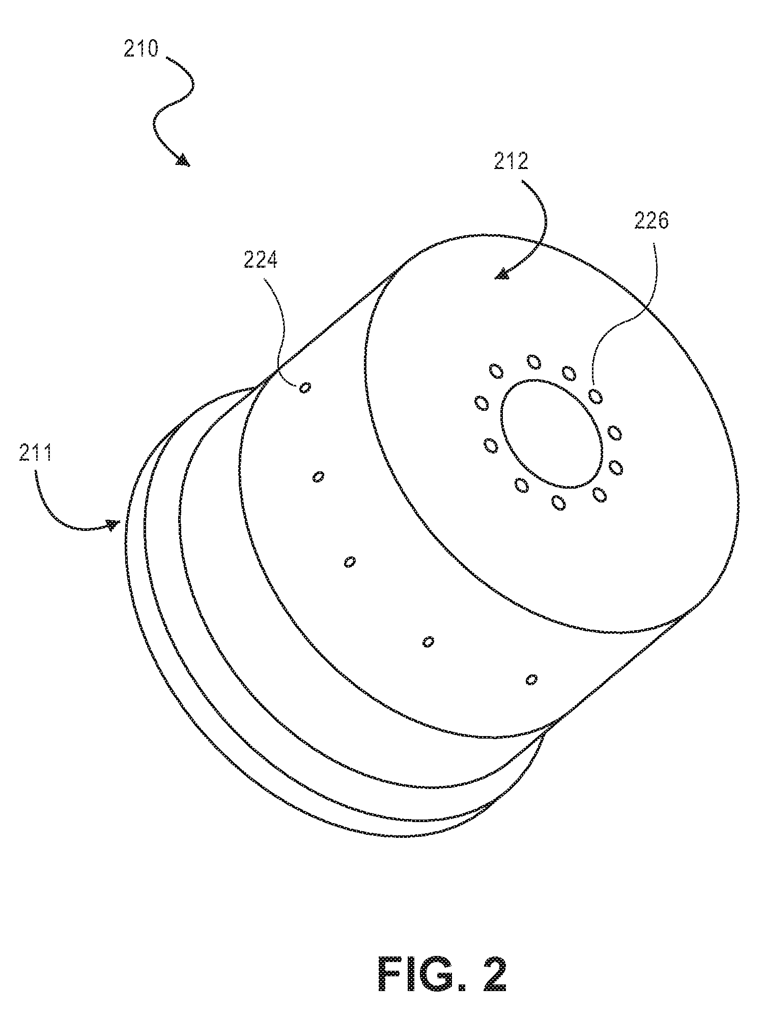
[0024] FIG. 2 illustrates an isometric view of a downstream side 212 of a gas nozzle 210, in accordance with an embodiment of the present invention. As shown, gas enters the nozzle 210 via the upstream side 211. In this particular embodiment, some portion of gas exits from the nozzle 210 via side holes 224, while the remainder exits through bottom holes 226 formed in the downstream side 212. While the exemplary embodiment illustrated in FIG. 2 includes both side holes 224 and bottom holes 226 to provide for enhanced tuning of a plasma process, any nozzle or showerhead configuration which includes exits holes in the downstream side 212 (with or without side holes 224) can suffer from a net accumulation of chamber coating 115.
[0025] In one embodiment the chamber coating 115 is an inorganic layer. In the exemplary conductor etch embodiment, the chamber coating 115 includes SiO.sub.x. A SiO.sub.x-based chamber coating is particularly advantageous for conductor etch applications, such as gate polysilicon or gate metal alloy etch operations because these etch processes generally have high selectivity to SiO, and the presence of SiO.sub.x on the chamber can reduce contamination of the workpiece by the chamber materials. However, it should be noted that the chamber coating 115 may include other constituents, such as Cl in a SiO.sub.xCl.sub.y coating formed where a SiCl.sub.4 source gas is employed to deposit the chamber coating 115. The chamber coating 115 may also be inorganic films other than the exemplary SiO, embodiment, for example the coating may be predominantly SiN. In still other embodiments, the chamber coating 115 is an organic coating, although such coatings generally lack the advantages of SiO.sub.x in a conductor etch applications.
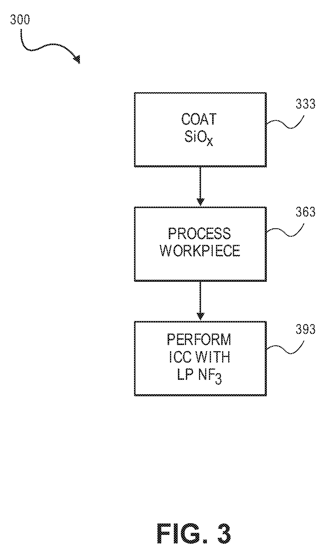
[0026] FIG. 3 is a flow diagram illustrating a chamber coat and clean process, in accordance with an embodiment of the present invention. Method 300 may be performed with a plasma processing system and more particular with a plasma etch system, such as that depicted in FIG. 5, during a fabrication process. At operation 333, an in-situ plasma chamber coating process is performed to deposit a chamber coating 115 in preparation for processing of a workpiece. In the exemplary embodiment, an SiO.sub.x-based coating is formed at operation 333. In one such embodiment, a silicon-containing source gas, such as but not limited to SiCl.sub.4, is employed with an oxidizing source gas, such as but not limited to O.sub.2 and N.sub.2O. Process pressures may be anywhere between 3 mT and 300 mT. Higher coating process pressures may reduce build up of coating material in the nozzle exit holes. However, in embodiments, the process pressure utilized in the coating operation 333 is to be less than the process pressure utilized in processing of the workpiece at operation 363 in an effort to ensure regions of the chamber which interact with the process plasma of operation 363 are not left uncoated by operation 333. Silicon source to oxidizer flow ratios between anywhere between 4:1 and 1:4 with 2:1 being an exemplary process for a SiCl.sub.4:O.sub.2 coating process. Coat process duration may be anywhere between about 10 and 60 seconds.
[0027] With the chamber coated, method 300 proceeds to operation 363 with processing of a workpiece. Generally, a workpiece may be any substrate conventionally employed in the fields of microelectronic, nanotechnology, photovoltaics, or the like. As one exemplary embodiment, the workpiece is a semiconductor wafer, such as, but not limited to silicon, germanium, or a commonly known III-V compound semiconductor material. As another embodiment, workpiece is a glass or sapphire material. In general, any plasma process commonly employed in the art may be performed at operation 363. In certain embodiments, a plasma etching of a workpiece is performed at operation 363 with the exemplary embodiment being a conductor etch process. Many conductor etch processes are known in the art and any etch applicable to polysilicon or any metal alloy in use for gate electrodes may be performed at operation 363. In a particular embodiment, the bulk of plasma etching at operation 363 is performed with a process having a selectivity of over 10:1 to the SiO.sub.x chamber coating and preferably over 20:1.
[0028] At operation 393, a low pressure ICC is performed to reset the state of the process chamber in preparation for processing of another workpiece. In the exemplary conductor etch embodiment, operation 393 is performed after the workpiece processed at operation 363 is unloaded from the chamber. In one such embodiment, the low pressure ICC operation 393 is performed without any dummy workpiece (e.g., waferless).
[0029] In an embodiment a low pressure ICC utilizes a first process gas including fluorine and a relatively low process pressure. Fluorine-based process gases are well-suited for etching most inorganic chamber coatings, particularly the exemplary SiO.sub.x-based coatings. While any of a number of known fluorine-based process gases, such as, but not limited to SF.sub.6 and CF.sub.4 may be used, in the exemplary embodiment NF.sub.3 is utilized. NF.sub.3 may offer an advantage of longer reactive species than does CF.sub.4, for example. In embodiments, a plasma of the first process gas is generated at a process pressure less than that utilized in processing of the workpiece. In certain embodiments, a plasma of the first process gas is generated at a process pressure no greater than 30 mT. This low pressure enhances the removal of coatings, such as SiOx-based coatings formed in gas nozzle exit holes. Generally, decreasing pressure below 30 mT will monotonically increase the mean free path, so pressures less than 10 mT are advantageous with pressures between 3 mT and 6 mT even more efficient at removing coatings formed in gas nozzle exit holes. In the exemplary conductor etch application where a SiO.sub.x coating is formed at operation 333, the SiO.sub.x-based coating is etched with a first process gas consisting only of NF.sub.3 at a pressure of 6 mT or less. A mixing of other source gases may be avoided for the benefit of lowest process pressure. However, in other embodiment, inerts such as He, Ar, or N.sub.2, etc, may be added in small amounts for benefit of plasma stability. Similarly, other reactive species such as Cl.sub.2 (or BCl.sub.3 where no oxidizer is present) may be added to the first process as long as the advantageous low process pressure is maintained. RF source power of between 1000 W and 4000 W may be utilized to energize the low pressure plasma with at least 2000 W offering an advantage of stability. RF bias power may be minimal to avoid damage to the chuck with the exemplary embodiment having an RF bias power of 0 W.
[0030] In an embodiment, the ICC operation 393 further includes a high pressure plasma clean utilizing a second process gas at a process pressure no less than 100 mT. In particular embodiments the high pressure plasma clean is performed at a pressure between 200 mT and 500 mT. In certain conductor etch embodiments, the second process gas includes at least NF.sub.3 at a pressure between 200 mT and 300 mT. In the exemplary conductor etch embodiment the second process gas includes NF.sub.3 along with at least one other reactive species, such as Cl.sub.2 and/or an oxidizer, such as O.sub.2, NO, CO, and COS. Addition of chlorine-based source gases may be useful for cleaning the chamber after a conductor etch involving an etching of a titanium alloy, such as TiN. Chlorine-containing source gas may also help to remove of AlF.sub.3 which may form on the chuck during operation 363. Addition of the oxidizer is useful for cleaning polymers which may be deposited on the chamber walls during the workpiece etch operation 363. For certain embodiments where an oxidizer is utilized, the high pressure clean is performed until an endpoint criteria is achieved indicating the carbonaceous polymers have been removed from the chamber. Inerts such as He, Ar, or N.sub.2, etc, may also be added to the high pressure clean. RF source power of between 1000 W and 4000 W may be utilized to energize the low pressure plasma with at least 1500 W offering an advantage of stability. RF bias power may be minimal to avoid damage to the chuck with the exemplary embodiment having an RF bias power of 0 W.
[0031] In particular embodiment, the high pressure clean of operation 393 is performed prior to the low pressure clean of operation 393. A high pressure clean performed first removes material deposited onto the chamber coating 115 during the etch operation 363 and may also remove a considerable amount of the chamber coating 115. The low pressure clean then cleans up any remainder of the chamber coating 115 and as such, may be a timed process performed for a predetermined duration of 5 to 30 seconds, for example. In further embodiments, a plasma is maintained during the transition from the high pressure clean to the low pressure clean to avoid striking the low pressure plasma.
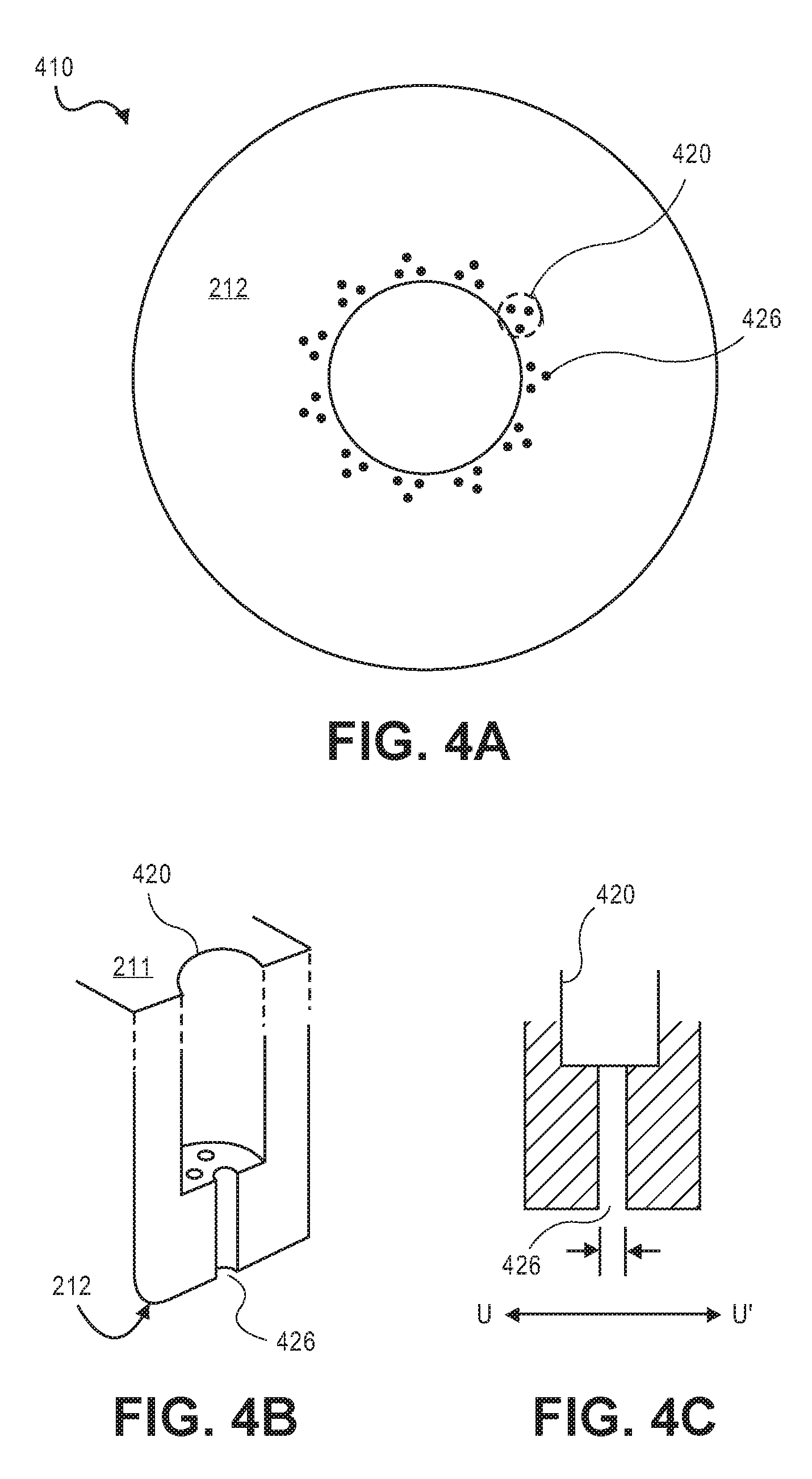
[0032] In an embodiment gas nozzle exit holes are constructed to reduce build up on chamber coatings, such as the exemplary SiO.sub.x coating. FIG. 4A illustrates a plan view of a downstream side 212 of a ytteria (Y.sub.2O.sub.3) gas nozzle 410, in accordance with an embodiment of the present invention. As shown, bottom exit holes 426 are dimensioned to be smaller than at least one entrance hole 420 having a first diameter recessed into an upstream side of the gas nozzle. In the exemplary embodiment, a plurality of bottom exit holes 426 are joined with a single entrance hole 420. For example, in the embodiment depicted in FIG. 4A, a bottom exit holes are arranged into subsets (e.g., twelve for depicted embodiment) with each subset including three bottom exit holes 426. Each of the exit holes in a subset has a diameter dimensioned so that each subset of exit holes occupies an area on the downstream side 212 that is no greater than an area the entrance hole 420 occupies on the upstream side of the gas nozzle.
[0033] FIG. 4B illustrates an isometric sectional view of a blend between the entrance hole 420 and subset of bottom exit holes 426 in the gas nozzle 410, in accordance with an embodiment. FIG. 4C illustrates a cross-sectional view of one bottom exit hole 426 while FIG. 4D illustrates plan view of on exit hole subset for the gas nozzle 410, in accordance with an embodiment of the present invention. As shown in FIG. 4C, the bottom exit hole 426 has a diameter D.sub.1. Generally, D.sub.1 is dimensioned to reduce formation of coatings, such as SiO.sub.x, on the inner surface of the bottom exit hole 426. In an embodiment, D.sub.1 is 800 .mu.m or less with little SiO.sub.x deposition observed for exit holes of 500 .mu.m and no SiO.sub.x deposits observed for exemplary embodiments with D.sub.1 of 300 .mu.m and less. With SiO.sub.x deposition found on larger diameter exit holes, hole diameter was found to decrease with chamber use, potentially adversely impacting a process plasma. As such, the low pressure cleans described elsewhere herein become more important for embodiments where diameters are greater than 800 .mu.m.
[0034] The position of the blend between entrance hole 420 and bottom exit hole 426 within the bulk of the nozzle 410 is varied based on conduction and uniformity requirements of the process with SiO.sub.x deposition reduced as a function of depth into the exit hole. Generally, the bottom exit hole 426 should have a recess depth of between 1 and 10 times D.sub.1, or about 250 .mu.m and 4000 .mu.m with the exemplary embodiment having a recess depth of at least five times D.sub.1. As shown in FIG. 4D, three bottom exit holes 426 are separated by a 120.degree. arc with G.sub.1 being between 250 and 300 .mu.m to arrive at a suitable minimum wall thickness for machining, 0.015'' for example. Reductions in D.sub.1 therefore permit a greater number of exit holes within a given area of the downstream side 412, with FIG. 4E illustrating a plan view of exit hole groups for gas nozzles in accordance with an alternate embodiment employing four bottom holes 426 separated by 90.degree. arcs with D.sub.1 of 250 .mu.m and maintaining 0.015'' wall thicknesses. Of course, other exit hole arrangements are possible without deviating from the advantageous dimensional properties illustrated by these exemplary embodiments.
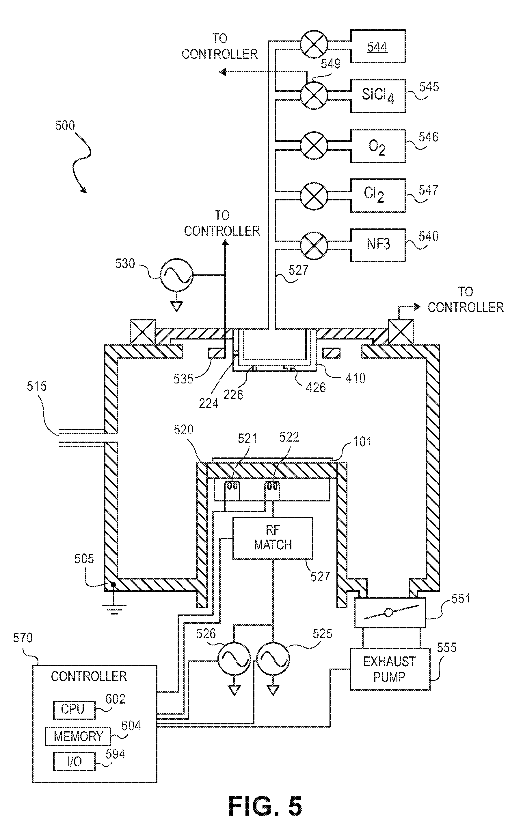
[0035] FIG. 5 is a schematic of a plasma etch system configured to perform the chamber coat and clean process, in accordance with an embodiment of the present invention. Exemplary embodiments of the plasma chamber coat and clean methods described herein may be performed with a plasma etch apparatus, such as the DPS AdvantEdge etch chamber manufactured by Applied Materials, Inc. of CA, USA. In another embodiment, all the plasma etch processes of method 200 are performed in the DPS AdvantEdge etch chamber, or alternate etch chamber designs, such as the , Enabler.TM., MxP.RTM., MxP+.TM., Super-ETM or E-MAX.RTM. chamber also manufactured by Applied Materials, Inc. of CA, USA. Other types of high performance etch chambers known in the art may also be used.
[0036] A cross-sectional view of an exemplary etch system 500 is shown in FIG. 5. System 500 includes a grounded chamber 505. A workpiece 101 is loaded through an opening 515 and clamped to a temperature controlled chuck 520. In particular embodiments, temperature controlled chuck 520 include a plurality of zones, each zone independently controllable to a temperature setpoint, such as with a first thermal zone 522 proximate a center of substrate 510 and a second thermal zone 521 proximate to a periphery of workpiece 101. Process gases, are supplied from gas sources 544, 545, 546, 547 and 548 through respective mass flow controllers 549 to the interior of the chamber 505. In certain embodiments, a gas nozzle 410 provides for distribution of process gases, such as a conductor etchant gas mixture 544. The gas nozzle 410 may include conventionally dimensioned bottom holes 226 or bottom exit holes 426, dimensioned as described elsewhere herein, for various embodiments. The gas nozzle 410 may further include side holes 224, as described elsewhere herein. As shown, the bottom exit holes 226 or 426 are disposed directly above the workpiece 101 with a downstream side of the gas nozzle 410 substantially parallel to the temperature controlled chuck 520.
[0037] In embodiments, periodic chamber coating is performed with SiCl.sub.4 source gas 545 and O.sub.2 source gas 546. In further embodiments, periodic chamber cleaning with NF.sub.3 source gas 540 is performed at a low pressure. Other chamber clean embodiments include addition cleaning with Cl.sub.2 source gas 547 and/or O.sub.2 source gas 546. During at least the low pressure NF.sub.3 chamber clean, the chamber 505 is evacuated to between 5 mTorr and 30 mTorr via an exhaust valve 551 connected to a high capacity vacuum pump stack 555 including a turbo molecular pump.
[0038] When RF power is applied processing of a workpiece or a chamber coat or ICC process described herein, a plasma is formed in chamber processing region over workpiece 101. Bias power RF generator 525 is coupled to the temperature controlled chuck 520. Bias power RF generator 525 provides bias power, if desired, to energize the plasma. Bias power RF generator 525 may have a low frequency between about 2 MHz to 60 MHz for example, and in a particular embodiment, is in the 13.56 MHz band. In certain embodiments, the plasma etch system 500 includes a third bias power RF generator 526 at a frequency at about the 2 MHz band which is connected to the same RF match 527 as bias power RF generator 525. Source power RF generator 530 is coupled through a match (not depicted) to a plasma generating element 535 to provide a source power to energize the plasma. Source RF generator 530 may have a frequency between 100 and 180 MHz, for example, and in a particular embodiment, is in the 162 MHz band. Because substrate diameters have progressed over time, from 150 mm, 200 mm, 300 mm, etc., it is common in the art to normalize the source and bias power of a plasma etch system to the substrate area.
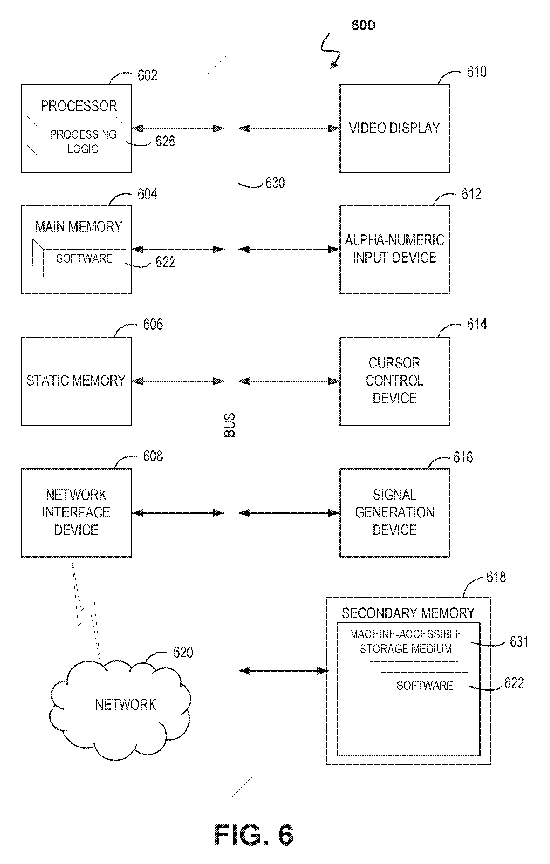
[0039] FIG. 6 illustrates a diagrammatic representation of a machine in the exemplary form of a computer system 600 which may be utilized to perform the ICC operations described herein. In one embodiment, the computer system 600 may be provisioned as the controller 570 in the plasma etch system 500. In alternative embodiments, the machine may be connected (e.g., networked) to other machines in a Local Area Network (LAN), an intranet, an extranet, or the Internet. The machine may operate in the capacity of a server or a client machine in a client-server network environment, or as a peer machine in a peer-to-peer (or distributed) network environment. The machine may be a personal computer (PC), a server, a network router, switch or bridge, or any machine capable of executing a set of instructions (sequential or otherwise) that specify actions to be taken by that machine (e.g., via commands set through I/O 594). Further, while only a single machine is illustrated, the term "machine" shall also be taken to include any collection of machines (e.g., computers) that individually or jointly execute a set (or multiple sets) of instructions to perform any one or more of the methodologies discussed herein.
[0040] The exemplary computer system 600 includes a processor 602, a main memory 604 (e.g., read-only memory (ROM), flash memory, dynamic random access memory (DRAM) such as synchronous DRAM (SDRAM) or Rambus DRAM (RDRAM), etc.), a static memory 606 (e.g., flash memory, static random access memory (SRAM), etc.), and a secondary memory 618 (e.g., a data storage device), which communicate with each other via a bus 630.
[0041] The processor 602 represents one or more general-purpose processing devices such as a microprocessor, central processing unit, or the like. The processor 602 may a general purpose device or a special-purpose processing device such as an application specific integrated circuit (ASIC), a field programmable gate array (FPGA), a digital signal processor (DSP), network processor, or the like. The processor 602 is configured to execute the processing logic 626 for performing the ICC operations discussed elsewhere herein.
[0042] The computer system 600 may further include a network interface device 608. The computer system 600 also may include a video display unit 610 (e.g., a liquid crystal display (LCD) or a cathode ray tube (CRT)), an alphanumeric input device 612 (e.g., a keyboard), a cursor control device 614 (e.g., a mouse), and a signal generation device 616 (e.g., a speaker).
[0043] The secondary memory 618 may include a machine-accessible storage medium (or more specifically a computer-readable storage medium) 631 on which is stored one or more sets of instructions (e.g., software 622) embodying any one or more of the ICC algorithms described herein. The software 622 may also reside, completely or at least partially, within the main memory 604 and/or within the processor 602 during execution thereof by the computer system 600, the main memory 604 and the processor 602 also constituting machine-readable storage media. The software 622 may further be transmitted or received over a network 620 via the network interface device 608.
[0044] The machine-accessible storage medium 631 may further be used to store a set of instructions for execution by a processing system and that cause the system to perform any one or more of the chucking and/or dechucking algorithms described herein. Embodiments of the present invention may further be provided as a computer program product, or software, that may include a machine-readable medium having stored thereon instructions, which may be used to program a computer system (or other electronic devices) to control a substrate chucking and dechucking temperatures according to the present invention as described elsewhere herein. A machine-readable medium includes any mechanism for storing \information in a form readable by a machine (e.g., a computer). For example, a machine-readable (e.g., computer-readable) medium includes a machine (e.g., a computer) readable storage medium (e.g., read only memory ("ROM"), random access memory ("RAM"), magnetic disk storage media, optical storage media, flash memory devices, and other non-transitory storage media.
[0045] Although the present invention has been described in language specific to structural features and/or methodological acts, it is to be understood that the invention defined in the appended claims is not necessarily limited to the specific features and embodiments described.
* * * * *
D00000
D00001
D00002
D00003
D00004
D00005
D00006
D00007
XML
uspto.report is an independent third-party trademark research tool that is not affiliated, endorsed, or sponsored by the United States Patent and Trademark Office (USPTO) or any other governmental organization. The information provided by uspto.report is based on publicly available data at the time of writing and is intended for informational purposes only.
While we strive to provide accurate and up-to-date information, we do not guarantee the accuracy, completeness, reliability, or suitability of the information displayed on this site. The use of this site is at your own risk. Any reliance you place on such information is therefore strictly at your own risk.
All official trademark data, including owner information, should be verified by visiting the official USPTO website at www.uspto.gov. This site is not intended to replace professional legal advice and should not be used as a substitute for consulting with a legal professional who is knowledgeable about trademark law.