Methods For Forming A Silicon Germanium Tin Layer And Related Semiconductor Device Structures
Bhargava; Nupur ; et al.
U.S. patent application number 15/985261 was filed with the patent office on 2019-01-10 for methods for forming a silicon germanium tin layer and related semiconductor device structures. The applicant listed for this patent is ASM IP Holding B.V.. Invention is credited to Nupur Bhargava, Joe Margetis, John Tolle.
| Application Number | 20190013199 15/985261 |
| Document ID | / |
| Family ID | 64903411 |
| Filed Date | 2019-01-10 |


| United States Patent Application | 20190013199 |
| Kind Code | A1 |
| Bhargava; Nupur ; et al. | January 10, 2019 |
METHODS FOR FORMING A SILICON GERMANIUM TIN LAYER AND RELATED SEMICONDUCTOR DEVICE STRUCTURES
Abstract
A method for forming a forming a silicon germanium tin (SiGeSn) layer is disclosed. The method may include, providing a substrate within a reaction chamber, exposing the substrate to a pre-deposition precursor pulse, which comprises tin tetrachloride (SnCl.sub.4), exposing the substrate to a deposition precursor gas mixture comprising a hydrogenated silicon source, germane (GeH.sub.4), and tin tetrachloride (SnCl.sub.4), and depositing the silicon germanium tin (SiGeSn) layer over a surface of the substrate. Semiconductor device structures including a silicon germanium tin (SiGeSn) layer formed by the methods of the disclosure are also provided.
| Inventors: | Bhargava; Nupur; (Phoenix, AZ) ; Margetis; Joe; (Gilbert, AZ) ; Tolle; John; (Gilbert, AZ) | ||||||||||
| Applicant: |
|
||||||||||
|---|---|---|---|---|---|---|---|---|---|---|---|
| Family ID: | 64903411 | ||||||||||
| Appl. No.: | 15/985261 | ||||||||||
| Filed: | May 21, 2018 |
Related U.S. Patent Documents
| Application Number | Filing Date | Patent Number | ||
|---|---|---|---|---|
| 62528818 | Jul 5, 2017 | |||
| Current U.S. Class: | 1/1 |
| Current CPC Class: | C23C 16/407 20130101; C23C 16/28 20130101; H01L 21/0262 20130101; C23C 16/401 20130101; H01L 21/02532 20130101; H01L 21/02381 20130101; H01L 21/02452 20130101; C23C 16/24 20130101; C23C 16/45523 20130101; H01L 21/02658 20130101; C23C 16/0272 20130101; C23C 16/14 20130101; H01L 21/02271 20130101; H01L 21/02535 20130101 |
| International Class: | H01L 21/02 20060101 H01L021/02; C23C 16/40 20060101 C23C016/40 |
Claims
1. A method for forming a silicon germanium tin (SiGeSn) layer, the method comprising: providing a substrate within a reaction chamber; exposing the substrate to a pre-deposition precursor pulse which comprises tin tetrachloride (SnCl.sub.4); exposing the substrate to a deposition precursor gas mixture comprising: a hydrogenated silicon source, germane (GeH.sub.4), and tin tetrachloride (SnCl.sub.4); and depositing the silicon germanium tin (SiGeSn) layer over a surface of the substrate.
2. The method of claim 1, wherein providing a substrate within the reaction chamber further comprises selecting the substrate to comprise a growth surface comprise at least one of silicon, germanium and silicon germanium (SiGe).
3. The method of claim 1, wherein exposing the substrate to the pre-deposition precursor pulse may further comprise forming a catalytic growth surface on the substrate.
4. The method of claim 1, wherein exposing the substrate to tin tetrachloride (SnCl.sub.4) further comprises exposing the substrate to tin tetrachloride (SnCl.sub.4) for time a period of between approximately 3 seconds to approximately 20 seconds.
5. The method of claim 1, wherein exposing the substrate to tin tetrachloride (SnCl.sub.4) further comprises exposing the substrate to germane (GeH.sub.4) and a forming a GeSn seed layer.
6. The method of claim 1, wherein forming a GeSn seed layer further comprises forming the GeSn seed layer with a thickness of between approximately 50 Angstroms and approximately 100 Angstroms.
7. The method of claim 1, further comprising selecting the hydrogenated silicon source to comprise at least one of: disilane (Si.sub.2H.sub.6), trisilane (Si.sub.3H.sub.8), or tetrasilane (Si.sub.4H.sub.10).
8. The method of claim 1, wherein the silicon germanium tin (SiGeSn) layer comprises an atomic percentage of silicon of greater than 2 at-%.
9. The method of claim 1, wherein the silicon germanium tin (SiGeSn) layer comprises an atomic percentage of germanium of greater than 80 at-%.
10. The method of claim 1, wherein the silicon germanium tin (SiGeSn) layer comprises an atomic percentage of tin of greater than 2 at-%.
11. The method of claim 1, wherein the silicon germanium tin (SiGeSn) layer comprises an epitaxial layer.
12. The method of claim 1, further comprising heating the substrate to a temperature of approximately less than 450.degree. C.
13. The method of claim 1, wherein depositing the silicon germanium tin (SiGeSn) layer over a surface of the substrate further comprises depositing the silicon germanium (SiGeSn) layer utilizing chemical vapor deposition.
14. A semiconductor device structure comprising the silicon germanium tin (SiGeSn) layer formed by the method of claim 1.
Description
CROSS-REFERENCE TO RELATED PATENT APPLICATION
[0001] The present disclosure claims the benefit of U.S. Provisional Patent Application No. 62/528,818, filed on Jul. 5, 2017 and entitled "METHODS FOR FORMING A SILICON GERMANIUM TIN LAYER AND RELATED SEMICONDUCTOR DEVICE STRUCTURES," which is incorporated herein by reference.
FIELD OF INVENTION
[0002] The present disclosure generally relates to methods for forming silicon germanium tin (SiGeSn) layers and related device structures containing a silicon germanium tin (SiGeSn) layer(s). The present disclosure also generally relates to chemical vapor deposition methods for depositing silicon germanium tin (SiGeSn) epitaxial layers.
BACKGROUND OF THE DISCLOSURE
[0003] There is a growing interest in tin-containing semiconductor materials like germanium tin (GeSn) and silicon germanium tin (SiGeSn) for many applications, such as, high mobility channel and strain engineering for advanced microelectronic devices, direct bandgap Group IV materials for photonic devices, or SiGeSn alloys for photovoltaic devices.
[0004] It has been found that the deposition of silicon germanium tin (SiGeSn) on certain substrate surfaces may be extremely difficult. As a non-limiting example, the formation of silicon germanium tin (SiGeSn) on the surface of a silicon substrate or on the surface of a germanium substrate may be extremely difficult and may be highly dependent on a number of factors, including, but not limited to, on the reactant precursors utilized for the deposition process. Accordingly, methods are desired for forming, e.g., depositing, silicon germanium tin (SiGeSn) layers utilizing optimized chemical precursors and conditions.
SUMMARY OF THE DISCLOSURE
[0005] In accordance with at least one embodiment of the disclosure, a method for forming a silicon germanium tin (SiGeSn) layer is disclosed. The method may comprise: providing a substrate within a reaction chamber, exposing the substrate to a pre-deposition precursor pulse which comprises tin tetrachloride (SnCl.sub.4), exposing the substrate to a deposition precursor gas mixture comprising a hydrogenated silicon source, germane (GeH.sub.4), and tin tetrachloride (SnCl.sub.4), and depositing the silicon germanium tin (SiGeSn) layer over a surface of the substrate. The embodiments of the disclosure may also include semiconductor device structures which may comprise a silicon germanium tin (SiGeSn) layer formed by the methods of the disclosure.
[0006] For purposes of summarizing the invention and the advantages achieved over the prior art, certain objects and advantages of the invention have been described herein above. Of course, it is to be understood that not necessarily all such objects or advantages may be achieved in accordance with any particular embodiment of the invention. Thus, for example, those skilled in the art will recognize that the invention may be embodied or carried out in a manner that achieves or optimizes one advantage or group of advantages as taught or suggested herein without necessarily achieving other objects or advantages as may be taught or suggested herein.
[0007] All of these embodiments are intended to be within the scope of the invention herein disclosed. These and other embodiments will become readily apparent to those skilled in the art from the following detailed description of certain embodiments having reference to the attached figures, the invention not being limited to any particular embodiment(s) disclosed.
BRIEF DESCRIPTION OF THE DRAWING FIGURES
[0008] While the specification concludes with claims particularly pointing out and distinctly claiming what are regarded as embodiments of the invention, the advantages of embodiments of the disclosure may be more readily ascertained from the description of certain examples of the embodiments of the disclosure when read in conjunction with the accompanying drawing, in which:
[0009] FIG. 1 illustrates a process flow diagram illustrating an exemplary deposition method in accordance with embodiments of the disclosure;
[0010] FIG. 2 illustrates two (2) theta x-ray diffraction (XRD) scans of example silicon germanium tin layers formed by the embodiments of the disclosure;
[0011] FIG. 3 illustrates a semiconductor device structure including a silicon germanium tin layer formed by the embodiments of the disclosure;
[0012] FIG. 4 illustrates a further semiconductor device structure including a silicon germanium tin layer formed by the embodiments of the disclosure; and
[0013] FIG. 5 illustrates a secondary ion mass spectroscopy (SIMS) depth profile scan of silicon germanium tin layers formed according to the embodiments of the disclosure.
[0014] It will be appreciated that elements in the figures are illustrated for simplicity and clarity and have not necessarily been drawn to scale. For example, the dimensions of some of the elements in the figures may be exaggerated relative to other elements to help improve understanding of illustrated embodiments of the present disclosure.
DETAILED DESCRIPTION OF EXEMPLARY EMBODIMENTS
[0015] Although certain embodiments and examples are disclosed below, it will be understood by those in the art that the invention extends beyond the specifically disclosed embodiments and/or uses of the invention and obvious modifications and equivalents thereof. Thus, it is intended that the scope of the invention disclosed should not be limited by the particular disclosed embodiments described below.
[0016] As used herein, the term "substrate" may refer to any underlying material or materials that may be used, or upon which, a device, a circuit or a film may be formed.
[0017] As used herein, the term "epitaxial layer" may refer to a substantially single crystalline layer upon an underlying substantially single crystalline substrate.
[0018] As used herein, the term "hydrogenated silicon source" may refer to a source of silicon having hydrogen incorporated therein.
[0019] As used herein, the term "chemical vapor deposition" may refer to any process wherein a substrate is exposed to one or more volatile precursors, which react and/or decompose on a substrate surface to produce a desired deposition.
[0020] As used herein, the term "silicon germanium tin" may refer to a material comprising silicon, germanium, and tin and may be represented as Si.sub.xGe.sub.1-xSn.sub.y wherein 1.gtoreq.x.gtoreq.0 and wherein 1.gtoreq.y.gtoreq.0.
[0021] The embodiments of the disclosure may include methods for forming silicon germanium tin (SiGeSn) layers and particularly for depositing silicon germanium tin (SiGeSn) layers by chemical vapor deposition. As a non-limiting example of the embodiments of the disclosure, the methods may include depositing a silicon germanium tin (SiGeSn) layer with a deposition precursor gas mixture comprising germane (GeH.sub.4) as the germanium source (or germanium precursor). The methods of chemical vapor deposition of silicon germanium tin (SiGeSn) layers as described herein therefore avoid the disadvantages associated with utilizing digermane (Ge.sub.2H.sub.6) as the germanium source, the disadvantages including, more complex packaging of the volatile source, increased costs, and limitations related to the selectivity of the chemical vapor deposition process utilizing digermane (Ge.sub.2H.sub.6).
[0022] In addition, a higher order silane may be utilized as the silicon source when forming silicon germanium tin (SiGeSn). For example, it is known to deposit silicon germanium tin (SiGeSn) utilizing silane (SiH.sub.4) as the silicon source, digermane (Ge.sub.2H.sub.6) as the germanium source, and tin tetrachloride as the source of tin. However, the deposition of silicon germanium tin (SiGeSn) preferably takes places at reduced substrate temperatures, for example, at a substrate temperature of less than 450.degree. C., and at such low temperatures, the disilane may not be sufficiently decomposed to produce enough reactive silicon species, thereby limiting the silicon atomic percentage that may be incorporated into the silicon germanium tin (SiGeSn) layer. In addition, the use of digermane (Ge.sub.2H.sub.6) is not ideal due to the volatile nature of the precursor, the cost of the precursor, and the lack of selectivity that can be achieved utilizing digermane (Ge.sub.2H.sub.6). Therefore, the embodiments of the disclosure provide methods for depositing silicon germanium tin (SiGeSn) that utilize alternative precursors, such as higher order silanes as the silicon source and germane (GeH.sub.4) as the germanium source.
[0023] However, the deposition of silicon germanium tin (SiGeSn) utilizing alternative precursors, such as higher order silanes and germane, is not straight forward and requires novel processing stages to enable high quality deposition. For example, utilizing a deposition method that comprises exposing a heated substrate to disilane (Si.sub.2H.sub.6) as the silicon source, germane (GeH.sub.4) as the germanium source, and tin tetrachloride (SnCl.sub.4) may result in little to no deposition and/or a delayed deposition of silicon germanium tin (SiGeSn) on the surface of the substrate with the possible additional formation of an interlayer of germanium (Ge) between the substrate and the deposited silicon germanium tin (SiGeSn).
[0024] Therefore, in particular embodiments of the disclosure, the methods of the disclosure may comprise exposing a substrate to a pre-deposition precursor pulse which may comprise tin tetrachloride (SnCl.sub.4) or alternatively may comprise both tin tetrachloride (SnCl.sub.4) and germane (GeH.sub.4). The utilization of the pre-deposition precursor pulse substantially reduces or even removes the delay in silicon germanium tin (SiGeSn) deposition and substantially reduces, or even eliminates, any formation of an interlayer of germanium (Ge) between the substrate and the deposited silicon germanium tin (SiGeSn) allowing for the deposition of silicon germanium tin (SiGeSn) over a number of substrate surfaces, including, but not limited to, silicon substrate surfaces and germanium substrate surfaces.
[0025] The methods of the disclosure may be understood with reference to FIG. 1 which illustrates a non-limiting example embodiment of a method for forming a silicon germanium tin (SiGeSn) layer. For example, FIG. 1 may illustrate a method 100 for forming a silicon germanium tin (SiGeSn) layer, which may comprise a process block 110 wherein a substrate may be provided into a reaction chamber and the substrate may be heated to process temperature within the reaction chamber. As a non-limiting example, the reaction chamber may comprise a reaction chamber of a chemical vapor deposition system. Embodiments of the present disclosure may be performed in a chemical vapor deposition system available from ASM International N.V. under the name Intrepid.TM. XP or Epsilon.RTM.. However, it is also contemplated that other reaction chambers and alternative chemical vapor deposition systems from other manufacturers may also be utilized to perform the embodiments of the present disclosure.
[0026] In some embodiments of the disclosure, the substrate may comprise a planar substrate or a patterned substrate. Patterned substrates may comprise substrates that may include semiconductor device structures formed into or onto a surface of the substrate, for example, the patterned substrates may comprise partially fabricated semiconductor device structures such as transistors and memory elements. The substrate may contain monocrystalline surfaces and/or one or more secondary surfaces that may comprise a non-monocrystalline surface, such as a polycrystalline surface and an amorphous surface. Monocrystalline surfaces may comprise, for example, one or more of silicon (Si), silicon germanium (SiGe), germanium tin (GeSn), or germanium (Ge). Polycrystalline or amorphous surfaces may include dielectric materials, such as oxides, oxynitrides or nitrides, such as, for example, silicon oxides and silicon nitrides.
[0027] In some embodiments of the disclosure, the substrate may comprise a "virtual substrate," in which a virtual substrate may comprise two or more materials disposed upon one another. For example, a germanium virtual substrate may comprise an upper most exposed germanium growth surface, wherein the virtual substrate may comprise a layer of germanium deposited on another material, e.g., a silicon substrate.
[0028] With continued reference to FIG. 1, the method 100 may continue by heating the substrate to a desired process temperature within a reaction chamber. In some embodiments of the disclosure, the method 100 may comprise heating the substrate to a temperature of less than approximately 450.degree. C., or to a temperature of less than approximately 400.degree. C., or to a temperature of less than approximately 350.degree. C., or to a temperature of less than approximately 300.degree. C., or even to a temperature of less than approximately 250.degree. C. In some embodiments of the disclosure, it may be desired to maintain the substrate at a reduced deposition temperature as the silicon germanium tin (SiGeSn) layer is unstable at higher deposition temperatures and such higher deposition temperatures may result in a phase separated silicon germanium tin (SiGeSn) layer of low quality, i.e., highly defective SiGeSn material.
[0029] Once the substrate is heated to the desired process temperature, the method 100 may continue by exposing the substrate to a pre-deposition pulse, as illustrated by a process block 120 of FIG. 1. In some embodiments of the disclosure, exposing the substrate to a pre-deposition pulse may comprise, exposing the substrate to a pre-deposition pulse which may comprise tin tetrachloride (SnCl.sub.4). As a non-limiting example embodiment of the disclosure, the substrate may be exposed to tin tetrachloride (SnCl.sub.4) for a time period of approximately greater than 3 seconds, or greater than 5 seconds, or even greater than 7 seconds. In some embodiments of the disclosure, during the pre-deposition pulse, the reaction chamber may be set to a pressure of less than or equal to approximately 760 mTorr, or less than approximately 400 mTorr, or even less than approximately 100 mTorr. In some embodiments of the disclosure, during the pre-deposition pulse the substrate temperature may be maintained at a temperature of approximately less than approximately 450.degree. C., or less than approximately 400.degree. C., or less than approximately 350.degree. C., or less than approximately 300.degree. C. or even less than approximately 250.degree. C. In some embodiments of the disclosure, during the pre-deposition pulse the flow rate of the tin tetrachloride is greater than approximately 3 mg/minute, or greater than approximately 5 mg/minute or even greater than approximately 10 mg/minute.
[0030] Not to be bound by theory, but it is believed that the pre-deposition precursor pulse may alter the surface energy of the substrate within the reaction chamber and thereby enable deposition on the surface of the substrate. It has been found that the embodiments of the disclosure alter the surface energy of the substrate such that silicon germanium tin (SiGeSn) deposition can be subsequently performed utilizing higher order silanes as the silicon source, germane as the germanium source, and tin tetrachloride (SnCl.sub.4) as the tin source.
[0031] In alternative embodiments of the disclosure, exposing the substrate to a pre-deposition precursor pulse may comprise, exposing the substrate to a pre-deposition precursor pulse that comprises both tin tetrachloride (SnCl.sub.4) and germane (GeH.sub.4). In such embodiments of the disclosure, the methods may comprise forming a germanium tin (GeSn) seed layer on the surface of the substrate, the germanium tin (GeSn) seed layer being formed by the reaction between the tin tetrachloride (SnCl.sub.4) and the germane (GeH.sub.4) utilized in the pre-deposition precursor pulse.
[0032] In some embodiments of the disclosure, exposing the substrate to a pre-deposition pulse may comprise, exposing the substrate to a pre-deposition pulse which may comprise both tin tetrachloride (SnCl.sub.4) and germane (GeH.sub.4). As a non-limiting example embodiment of the disclosure the substrate may be exposed to both tin tetrachloride (SnCl.sub.4) and germane (GeH.sub.4) for a time period of approximately great than 5 second, or greater than 10 seconds, or even greater than 15 seconds. In some embodiments of the disclosure, during the pre-deposition pulse the reaction chamber may be set to a pressure of less than or equal to approximately 760 mTorr, or less than approximately 400 mTorr, or even less than approximately 100 mTorr. In some embodiments of the disclosure, during the pre-deposition pulse the substrate temperature may be maintained at a temperature of approximately less than 450.degree. C., or less than 400.degree. C., or less than 350.degree. C., or less than 300.degree. C., or even less than 250.degree. C. In some embodiments of the disclosure, during the pre-deposition pulse, the flow rate of the tin tetrachloride may be approximately greater than approximately 3 mg/minute, or greater than approximately 5 mg/minute, or even greater than approximately 10 mg/minute. In some embodiments of the disclosure, during the pre-deposition pulse, the flow rate of the germane may be approximately greater than 10 sccm, or greater than approximately 200 sccm, or even greater than approximately 300 sccm.
[0033] Again, not to be bound by theory, but it is believed that the formation of the germanium tin (GeSn) seed layer changes the surface energy of the substrate and thereby allows subsequent deposition of a silicon germanium tin (SiGeSn) layer over the germanium tin (GeSn) seed layer. Therefore, in some embodiments of the disclosure exposing the substrate to the pre-deposition precursor pulse may further comprise forming a catalytic growth surface on the substrate. In some embodiments of the disclosure, the methods may comprise, forming a germanium tin (GeSn) seed layer with a thickness of between approximately 50 Angstroms and approximately 100 Angstroms.
[0034] Once the substrate has been exposed to the pre-deposition precursor pulse, the substrate may be further exposed to a deposition gas mixture for depositing a layer of silicon germanium tin (SiGeSn) over a surface of the substrate. As illustrated by a process block 130 of FIG. 1, exposing the substrate to a deposition precursor gas mixture may comprise, selecting the deposition precursor gas mixture to comprise a hydrogenated silicon source, germane (GeH.sub.4) and tin tetrachloride (SnCl.sub.4). For example, the method 100 and particularly the process block 130 may comprise, selecting the hydrogenated silicon source to comprise at least one of: disilane (Si.sub.2H.sub.6), trisilane (Si.sub.3H.sub.8), or tetrasilane (Si.sub.4H.sub.10). In addition, the hydrogenated silicon source may comprise higher silanes with the general empirical formula Si.sub.xH.sub.(2x+2).
[0035] In some embodiments of the disclosure, exposing the substrate to a deposition precursor gas mixture further comprises, maintaining the reaction chamber to a pressure of less than or equal to approximately 760 mTorr, or less than approximately 400 mTorr, or even less than approximately 100 mTorr. In some embodiments of the disclosure, during the exposure of the substrate to the deposition precursor gas mixture the substrate temperature may be maintained at a temperature of approximately less than 450.degree. C., or less than 400.degree. C., or less than 350.degree. C., or less than 300.degree. C., or even less than 250.degree. C. In some embodiments of the disclosure, during the exposure of the substrate to the deposition precursor gas mixture the flow rate of the tin tetrachloride may be approximately greater than approximately 3 mg/minute, or greater than approximately 5 mg/minute, or even greater than approximately 10 mg/minute. In some embodiments of the disclosure, during the exposure of the substrate to a deposition precursor gas mixture the flow rate of the germane may be approximately greater than 100 sccm, or greater than approximately 200 sccm, or even greater than approximately 400 sccm. In some embodiments of the disclosure, during the exposure of the substrate to a deposition precursor gas mixture the flow rate of the hydrogenated silicon source (e.g., disilane) may be approximately greater than 3 sccm, or greater than approximately 10 sccm, or even greater than approximately 20 sccm.
[0036] In exposing the substrate to the deposition precursor gas mixture, the method 100 may comprise a process block 140 wherein the method further comprises depositing a silicon germanium tin (SiGeSn) layer over the substrate. In some embodiments of the disclosure, the silicon germanium tin (SiGeSn) layer may be deposited to a thickness of greater than approximately 100 Angstroms, or greater than approximately 500 Angstroms, or even greater than approximately 1000 Angstroms. In some embodiments of the disclosure, the growth rate of the silicon germanium tin (SiGeSn) utilizing the methods of the disclosure may be greater than approximately 10 Angstroms/minute, or greater than approximately 25 Angstroms/minute, or even greater than approximately 50 Angstroms/minute.
[0037] In some embodiments of the disclosure, the silicon germanium tin (SiGeSn) layer may comprise an atomic percentage (at-%) of silicon of greater than approximately 2 at-%, or greater than approximately 10 at-%, or even greater than approximately 30 at-%. In some embodiments of the disclosure, the silicon germanium tin (SiGeSn) layer may comprise an atomic percentage of germanium of greater than approximately 80 at-%, or greater than approximately 90 at-%, or even greater than 95 at-%. In further embodiments of the disclosure, the silicon germanium tin (SiGeSn) layer may comprise an atomic percentage of tin of greater than approximately 2 at-%, or greater than approximately 10 at-%, or even greater than approximately 20 at-%.
[0038] In some embodiments a silicon germanium tin (SiGeSn) layer comprising silicon, germanium and tin may comprise less than about 20 at-%, or less than about 10 at-%, or less than about 7 at-%, or less than about 5 at-%, or less than about 3 at-%, or less than about 2 at-%, or less than about 1 at-% of impurities, that is, elements other than Si, Ge or Sn. In some embodiments the silicon germanium tin layer comprising silicon, germanium, and tin comprises less than about 20 at-%, or less than about 10 at-%, or less than about 5 at-%, or less than about 2 at-%, or less than about 1 at-% of hydrogen. In some embodiments the silicon germanium tin layer comprising silicon, germanium, and tin may comprise less than about 10 at-%, or less than about 5 at-%, or less than about 2 at-%, or less than about 1 at-%, or even less than about 0.5 at-% of carbon. In some embodiments the silicon germanium tin layer comprising silicon, germanium, and tin may comprise less than about 5 at-%, or less than about 2 at-%, or less than about 1 at-%, or less than about 0.5 at-%, or even less than about 0.2 at-% of nitrogen. In some embodiments the silicon germanium tin layer may comprise less than about 15 at-%, or less than about 10 at-%, or less than about 5 at-%, or less than about 3 at-%, or less than about 2 at-%, or even less than about 1 at-% of oxygen. In some embodiments the silicon germanium tin layer may comprise less than about 30 at-%, or less than about 20 at-%, or less than about 20 at-%, or less than about 5 at-%, or even less than about 3 at-% of oxygen on average at the surface, wherein the surface can be understood to be thickness of less than about 20 nm from the top most surface. In some embodiments the thin film comprising silicon, germanium, and tin may comprise more than about 80 at-%, or more than about 90 at-%, or more than about 93 at-%, or more than about 95 at-%, or more than about 97 at-%, or more than about 99 at-% silicon, germanium, and tin.
[0039] In some embodiments, the silicon germanium tin (SiGeSn) layer may be deposited on a three-dimensional structure. In some embodiments, the step coverage of the SiGeSn layer comprising silicon, germanium, and tin may be equal to or greater than about 50%, greater than about 80%, greater than about 90%, about 95%, about 98% or about 99% or greater in structures having aspect ratios (height/width) of more than about 2, more than about 5, more than about 10, more than about 25, more than about 50 or more than about 100. As used herein, the term "step coverage" is defined as percentage ratio of a thickness of the SiGeSn film on a sidewall of the substrate to the thickness of the SiGeSn film on a horizontal surface of the substrate.
[0040] FIG. 2 illustrates a graph 200 showing the 2 theta x-ray diffraction (XRD) scans of example silicon germanium tin layers formed by methods of the current disclosure. In this non-limiting example, the substrate comprises a virtual substrate further comprising a buffer layer of germanium deposited on an underlying silicon substrate. The XRD scan labelled as 202 illustrates the process of depositing silicon germanium tin (SiGeSn) without the utilization of the pre-deposition pulse. As illustrated by the XRD scan labelled 202, both the XRD peaks for the germanium buffer layer and the underlying silicon substrate are visible but there is no discernable XRD peak to indicate the deposition of any silicon germanium tin (SiGeSn). Therefore the XRD scan labelled 202 illustrates that without utilizing the pre-deposition pulse, little to no silicon germanium tin (SiGeSn) is deposited on the substrate. In contrast, the XRD scan labelled as 204 illustrates a deposition according to the embodiments of the current disclosure which includes a pre-deposition pulse. Reviewing the XRD scan labelled 204, the XRD peaks for both the germanium buffer layer and the underlying substrate can be seen, however, there is an additional XRD shoulder labelled 206 which indicates the presence of silicon germanium tin on the surface of the substrate. Therefore, the graph 200 in FIG. 2 illustrates that deposition of silicon germanium tin (SiGeSn) on a germanium virtual substrate may require a pre-deposition pulse process prior to silicon germanium tin deposition to ensure successful deposition of the silicon germanium tin (SiGeSn) layer.
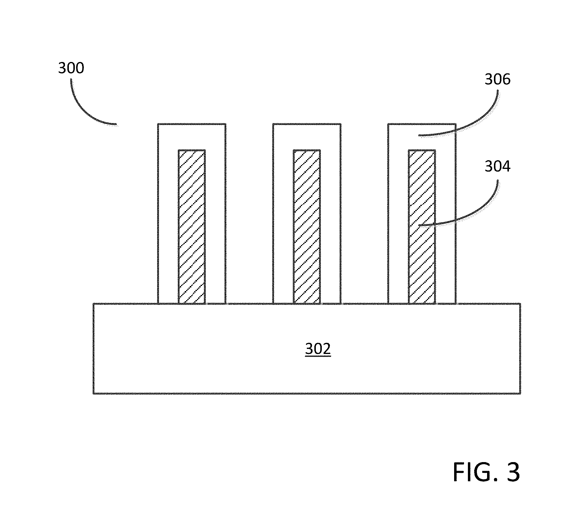
[0041] The embodiments of the disclosure may also provide semiconductor device structures comprising one or more silicon germanium tin (SiGeSn) layers formed by the methods described herein. For example, FIG. 3 illustrates a non-limiting example of a semiconductor device structure 300, wherein the semiconductor device structure comprises a partially fabricated double gate MOSFET, commonly referred to as a FinFET. The semiconductor device structure 300 may comprise a substrate 302, an initial Fin structure 304, and a secondary Fin layer 306 formed by the embodiments of the current disclosure. In some embodiments of the disclosure, the secondary Fin layer 306 may comprise a silicon germanium tin (SiGeSn) layer and the initial Fin structure 304 may comprise germanium (Ge). As a non-limiting example, the deposition of the silicon germanium tin (SiGeSn) layer 306 on the germanium (Ge) initial Fin structure 304 may comprise an initial pre-deposition pulse of tin tetrachloride (SnCl.sub.4) to enable substantial direct deposition of the silicon germanium tin (SiGeSn) layer 306 without the formation of an intermediate germanium layer, as may occur without the use of the pre-deposition pulse process. The device performance of the FinFET device 300 is dependent on the critical dimensions of the device, particularly the critical dimensions of the initial Fin structure 304, therefore the embodiments of the disclosure enable the direct deposition of silicon germanium tin (SiGeSn) on the initial germanium Fin structure 304 without the deposition of an undesirable germanium layer which could alter the critical dimensions of the FinFET device structure 300.
[0042] As a further non-limiting semiconductor device structure example, FIG. 4 illustrates the partially fabricated optoelectronic device 400 including a silicon germanium tin (SiGeSn) layer 408. The semiconductor device structure 400 includes a substrate 402 which may comprise a silicon substrate and a buffer layer 404 which may comprise a germanium buffer layer disposed over the silicon substrate 402. The semiconductor device structure 400 may also comprise an active region 412, disposed over the germanium buffer layer, the active region comprising cladding layer 406 and cladding layer 410 with a quantum well layer 408 disposed between the two cladding layers. In some embodiments of the disclosure the cladding layers 406 and 410 may comprise germanium tin (GeSn) with a tin composition of approximately 5 at-% and the quantum well layer 408 may comprise a silicon germanium tin (SiGeSn) layer with a tin composition of between approximately 10-15 at-%.
[0043] The quality of the interfaces 414 and 416 between the cladding layers 406 and 410 and the quantum well layer 408 may have a direct influence on the quality of the optoelectronic device structure fabricated from semiconductor device structure 400. Therefore the methods of the current disclosure ensure that prior to the deposition of the silicon germanium tin (SiGeSn) quantum well layer 408, the upper surface of the lower cladding layer 406 is subjected to a pre-deposition pulse, e.g., a pulse of tin tetrachloride, such that the interface between the lower cladding layer 406 and the quantum well layer 408 may be smooth, well defined and substantially free of an intermediate germanium layer which may occur without the methods of the current disclosure.
[0044] FIG. 5 illustrates a secondary ion mass spectroscopy (SIMS) depth profile scan of silicon germanium tin layers formed according to the embodiments of the disclosure. The data labelled as 502 illustrates the atomic percentage of germanium and the data labelled as 504 illustrates the atomic percentage of tin. The region of the SIMS depth profile scan labelled as 506 (the region between approximately 40 nanometers and approximately 60 nanometers depth) illustrates the change in the concentration of germanium and tin during the attempted deposition of a silicon germanium tin layer without the use of a pre-deposition pulse. In contrast, the region of the SIMS depth profile scan labelled as 508 (the region between approximately 110 nanometers and approximately 130 nanometers depth) illustrates the change in the concentration of germanium and tin during the deposition of a silicon germanium tin layer utilizing the pre-deposition pulse process. In SIMS depth profile analysis the thickness of a particular feature may be determined by the integration of the area of the "dip" in the profile scan. As can be observed from FIG. 5 the "dip" in the concentration of germanium is far more pronounced in region 506 when compared with region 508. Therefore the data in FIG. 5 illustrates that the embodiments the disclosure result in a much thinner undesirable germanium layer when utilizing the pre-deposition pulse if compared with results obtained without the pre-deposition pulse.
[0045] The example embodiments of the disclosure described above do not limit the scope of the invention, since these embodiments are merely examples of the embodiments of the invention, which is defined by the appended claims and their legal equivalents. Any equivalent embodiments are intended to be within the scope of this invention. Indeed, various modifications of the disclosure, in addition to those shown and described herein, such as alternative useful combination of the elements described, may become apparent to those skilled in the art from the description. Such modifications and embodiments are also intended to fall within the scope of the appended claims.
* * * * *
D00000
D00001
D00002
D00003
D00004
D00005
XML
uspto.report is an independent third-party trademark research tool that is not affiliated, endorsed, or sponsored by the United States Patent and Trademark Office (USPTO) or any other governmental organization. The information provided by uspto.report is based on publicly available data at the time of writing and is intended for informational purposes only.
While we strive to provide accurate and up-to-date information, we do not guarantee the accuracy, completeness, reliability, or suitability of the information displayed on this site. The use of this site is at your own risk. Any reliance you place on such information is therefore strictly at your own risk.
All official trademark data, including owner information, should be verified by visiting the official USPTO website at www.uspto.gov. This site is not intended to replace professional legal advice and should not be used as a substitute for consulting with a legal professional who is knowledgeable about trademark law.