Pitch Reduction Technology Using Alternating Spacer Depositions During the Formation of a Semiconductor Device and Systems Including Same
Zhou; Baosuo ; et al.
U.S. patent application number 15/681066 was filed with the patent office on 2017-12-28 for pitch reduction technology using alternating spacer depositions during the formation of a semiconductor device and systems including same. This patent application is currently assigned to Micron Technology, Inc.. The applicant listed for this patent is Micron Technology, Inc.. Invention is credited to Mirzafer K. Abatchev, Brian J. Coppa, Joseph Neil Greeley, Shuang Meng, Paul A. Morgan, Ardavan Niroomand, Baosuo Zhou.
| Application Number | 20170372913 15/681066 |
| Document ID | / |
| Family ID | 38919499 |
| Filed Date | 2017-12-28 |


View All Diagrams
| United States Patent Application | 20170372913 |
| Kind Code | A1 |
| Zhou; Baosuo ; et al. | December 28, 2017 |
Pitch Reduction Technology Using Alternating Spacer Depositions During the Formation of a Semiconductor Device and Systems Including Same
Abstract
A method for patterning a layer increases the density of features formed over an initial patterning layer using a series of self-aligned spacers. A layer to be etched is provided, then an initial sacrificial patterning layer, for example formed using optical lithography, is formed over the layer to be etched. Depending on the embodiment, the patterning layer may be trimmed, then a series of spacer layers formed and etched. The number of spacer layers and their target dimensions depends on the desired increase in feature density. An in-process semiconductor device and electronic system is also described.
| Inventors: | Zhou; Baosuo; (Boise, ID) ; Abatchev; Mirzafer K.; (Fremont, CA) ; Niroomand; Ardavan; (Boise, ID) ; Morgan; Paul A.; (Kuna, ID) ; Meng; Shuang; (Austin, TX) ; Greeley; Joseph Neil; (Boise, ID) ; Coppa; Brian J.; (Tempe, AZ) | ||||||||||
| Applicant: |
|
||||||||||
|---|---|---|---|---|---|---|---|---|---|---|---|
| Assignee: | Micron Technology, Inc. Boise ID |
||||||||||
| Family ID: | 38919499 | ||||||||||
| Appl. No.: | 15/681066 | ||||||||||
| Filed: | August 18, 2017 |
Related U.S. Patent Documents
| Application Number | Filing Date | Patent Number | ||
|---|---|---|---|---|
| 15076474 | Mar 21, 2016 | 9761457 | ||
| 15681066 | ||||
| 14507507 | Oct 6, 2014 | 9305782 | ||
| 15076474 | ||||
| 11484271 | Jul 10, 2006 | 8852851 | ||
| 14507507 | ||||
| Current U.S. Class: | 1/1 |
| Current CPC Class: | H01L 23/564 20130101; H01L 21/3088 20130101; H01L 21/30625 20130101; H01L 21/30604 20130101; H01L 21/0338 20130101; H01L 21/0335 20130101; H01L 2924/0002 20130101; H01L 21/0337 20130101; H01L 21/3086 20130101; H01L 2924/0002 20130101; H01L 2924/00 20130101 |
| International Class: | H01L 21/306 20060101 H01L021/306; H01L 23/00 20060101 H01L023/00; H01L 21/033 20060101 H01L021/033; H01L 21/308 20060101 H01L021/308 |
Claims
1-29 (canceled)
30. A method used during fabrication of a semiconductor device, the method comprising: forming a pair of sacrificial pedestals on a layer to be etched; forming a spacer layer over at least the pair of sacrificial pedestals; removing the pair of sacrificial pedestals and a portion of the spacer layer to form pairs of sacrificial spacers, each of the pairs of sacrificial spacers having one spacer closest to another spacer of the other pair and defining a space between the one and the other spacer; and filling the space between the one and the other sacrificial spacer to form a spacer used during etching of the layer to be etched.
31. The method of claim 30 wherein the spacer comprises silicon nitride.
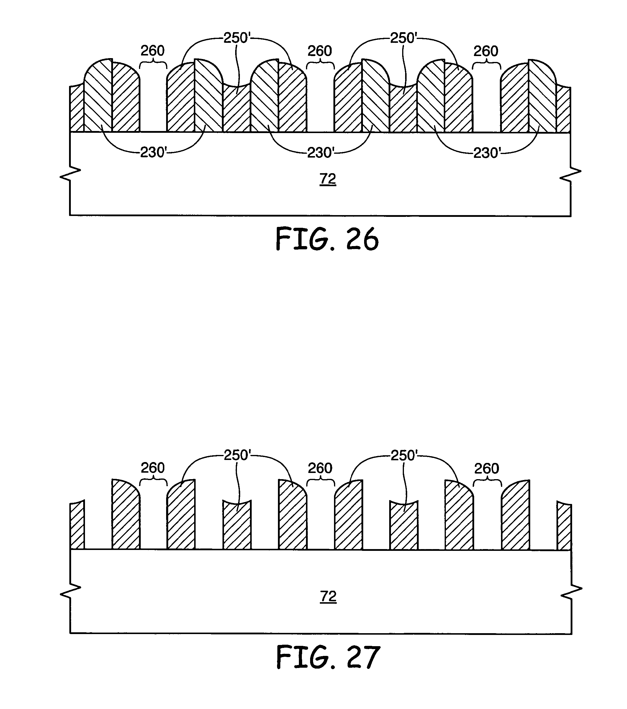
32. The method of claim 30 wherein each of the sacrificial spacers are formed from one of two different types of materials.
33. The method of claim 30 further comprising when filling the space, forming second spacers along the sides of the sacrificial spacers.
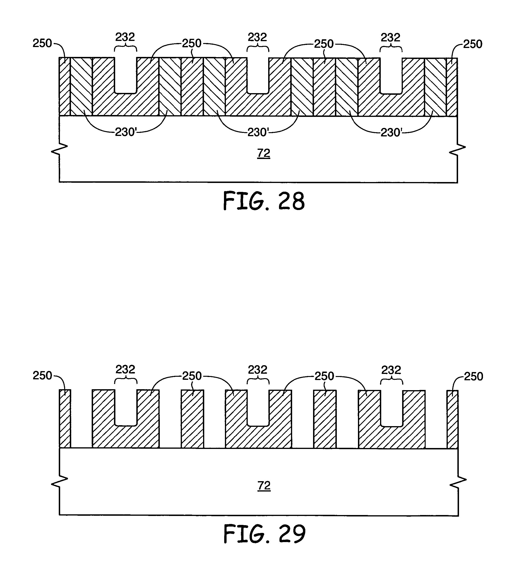
34. The method of claim 30 further comprising removing the sacrificial spacers prior to etching the layer to be etched.
35. A method used during fabrication of a semiconductor device, the method comprising: forming a pair of sacrificial pedestals on a layer to be etched; forming a spacer layer over at least the pair of sacrificial pedestals; removing the pair of sacrificial pedestals and a portion of the spacer layer to form pairs of sacrificial spacers; and filling the space previously occupied by the sacrificial pedestals with spacer material, the spacer material extending to the walls of the sacrificial spacers and the layer to be etched between the sacrificial spacers.
36. The method of claim 35 wherein the spacer material comprises silicon nitride.
37. The method of claim 35 further comprising planarizing the sacrificial spacers and the spacer material.
38. The method of claim 37 further comprising removing the sacrificial spacers.
39. The method of claim 38 further comprising etching the layer to be etched, the etching removing at least a portion of the spacer material.
40. The method of claim 35 wherein the spacer material is formed into a U-shape between the sacrificial spacers.
Description
FIELD OF THE INVENTION
[0001] This invention relates to the field of semiconductor manufacture and, more particularly, to a method for forming features at a starting feature density with a lithography mask, and resulting in a final density which is n times of the first density, where n is an integer greater than 1, through the use of various conformal layers and selective etches.
BACKGROUND OF THE INVENTION
[0002] During the formation of a semiconductor device, many features such as word lines, digit lines, contacts, and other features are commonly formed over a semiconductor wafer. A goal of semiconductor device engineers is to form as many of these features in a given area as possible to increase yields, decrease manufacturing costs, and to miniaturize devices. The formation of these structures on a semiconductor wafer typically requires the use of lithography. Optical lithography, the lithographic method most used in leading-edge wafer processing, comprises projecting coherent light of a given wavelength, typically 248 nanometers (nm) or 193 nm, from an illumination source (illuminator) through a quartz photomask or reticle having a chrome pattern representative of features to be formed, and imaging that pattern onto a wafer coated with photoresist. The light chemically alters the photoresist and enables the exposed photoresist (if positive resist is used) or the unexposed photoresist (if negative resist is used) to be rinsed away using a developer.
[0003] With decreasing feature sizes, the limits of optical lithography are continually being tested. Improvements in feature density are made through process advances, enhanced lithographic methods referred to as resolution enhancement techniques, and improved equipment and materials.
[0004] One such process advance, depicted in FIGS. 1-6, uses a mask having repeating features of a given pitch (i.e. a given distance from the beginning of one repeating feature to the beginning of the next feature) along with the formation of various layers and selective etches to double the density of the features formed from the lithography mask. FIG. 1 depicts a semiconductor wafer substrate assembly 10 comprising a semiconductor wafer, a layer to be etched 12, for example a silicon nitride layer, a support layer 14, for example formed from carbon using chemical vapor deposition (CVD) or a spin-on technique, and a patterned masking layer 16, such as a photoresist layer formed using an optical lithographic process or a hard mask layer formed using optical lithography and an etch process. The patterned masking layer 16 may be formed at the feature size limits allowed by the lithographic process, and comprises three individual features (three periods/pitches) formed over a given distance 18.
[0005] After forming the structure of FIG. 1, an etch of the support layer 14 is performed using mask 16 as a pattern. This etch is typically an anisotropic dry etch which etches the support layer 14 selective to the layer to be etched 12 (i.e. which removes the support layer 14 with little or no etching of the layer to be etched 12). After etching the support layer 14, the patterned masking layer 16 is removed and a conformal hard mask layer 20, for example silicon dioxide, is formed to result in the structure of FIG. 2.
[0006] Subsequently, a spacer etch of the FIG. 2 structure is performed to result in the structure of FIG. 3 having spacers 20' from the hard mask layer along sidewalls of the support layer 14. Subsequently, the support layer 14 is etched to result in the structure of FIG. 4.
[0007] Next, spacers 20' formed from the hard mask layer are used as a pattern to etch the layer to be etched 12, which results in the structure of FIG. 5. Finally, spacers 20' are etched selective to the layer to be etched 12 to result in the structure of FIG. 6.
[0008] The process of FIGS. 1-6 has the advantage of using optical lithography to form the masking layer 16 having three features in a given distance 18, while the completed structure depicted in FIG. 6 has six features 12 (six periods/pitches) in the original distance 18. Thus the number of features within the distance is approximately doubled without requiring an additional lithography mask.
[0009] Various techniques to increase feature density are described in U.S. Pat. No. 5,328,810 by Tyler A. Lowrey, et al. and U.S. Pat. No. 5,254,218 by Ceredig Roberts et al., both of which are assigned to Micron Technology, Inc. and incorporated herein as if set forth in their entirety.
[0010] A method for forming a semiconductor device using an optical lithography mask with a first pitch and resulting in features having a second pitch equal to 1/n, where n is an integer greater than 1 and without limitation of feature size reduction or spacing to one-half of that attainable using lithography, would be desirable.
BRIEF DESCRIPTION OF THE DRAWINGS
[0011] FIGS. 1-6 are cross sections depicting a conventional process for doubling the number of mask features, for example formed using photolithography;
[0012] FIGS. 7-15 are cross sections of an in-process semiconductor device depicting an embodiment of the inventive method which increases the number of features in a given area by four times;
[0013] FIGS. 16-22 are cross sections depicting an embodiment of the inventive method which increases the number of features in a given area by six times;
[0014] FIGS. 23-31 are cross sections depicting another embodiment and variations of the inventive method which increases the number of features in a given area by three times;
[0015] FIGS. 32-38 are cross sections depicting another embodiment of the invention which increases the number of features in a given area by five times;
[0016] FIG. 39 is an isometric depiction of various components which may be manufactured using devices formed with an embodiment of the present invention; and
[0017] FIG. 40 is a block diagram of an exemplary use of the invention to form part of a memory device having a storage transistor array.
[0018] It should be emphasized that the drawings herein may not be to exact scale and are schematic representations. The drawings are not intended to portray the specific parameters, materials, particular uses, or the structural details of the invention, which may be determined by one of skill in the art by examination of the information herein.
DETAILED DESCRIPTION OF THE ILLUSTRATED EMBODIMENTS
[0019] The term "wafer" is to be understood as a semiconductor-based material including silicon, silicon-on-insulator (SOI) or silicon-on-sapphire (SOS) technology, doped and undoped semiconductors, epitaxial layers of silicon supported by a base semiconductor foundation, and other semiconductor structures. Furthermore, when reference is made to a "wafer" in the following description, previous process steps may have been utilized to form regions or junctions in or over the base semiconductor structure or foundation. Additionally, when reference is made to a "substrate assembly" in the following description, the substrate assembly may include a wafer with layers including dielectrics and conductors, and features such as transistors, formed thereover, depending on the particular stage of processing. In addition, the semiconductor need not be silicon-based, but may be based on silicon-germanium, silicon-on-insulator, silicon-on-sapphire, germanium, or gallium arsenide, among others. Further, in the discussion and claims herein, the term "on" used with respect to two layers, one "on" the other, means at least some contact between the layers, while "over" means the layers are in close proximity, but possibly with one or more additional intervening layers such that contact is possible but not required. Neither "on" nor "over" implies any directionality as used herein. The term "about" indicates that the value listed may be somewhat altered, as long as the alteration does not result in nonconformance of the process or structure in question to the present invention. A "spacer" indicates a layer, typically dielectric, formed as a conformal layer over uneven topography then anisotropically etched to remove horizontal portions of the layer and leave taller, vertical portions of the layer.
[0020] Various embodiments of the present invention use alternating spacer deposition (ASD) for pitch reduction to achieve variable critical dimension (CD) reduction ratios. The pitch reduction process achieves a CD which is smaller than that defined by a previously formed photolithography mask. The various process embodiments described herein comprise the use of a first type of spacer material used as a sacrificial layer and removed with high selectivity to a second spacer material which is used to pattern an underlying layer. Depending upon the trim ratio, the number of spacer depositions, and the thickness of each deposition, a CD which is 1/n of the original value defined by prior photolithography may be achieved, where n is an odd or even integer greater than 1. In other words, the process multiplies the pattern density by n times. Particularly, by repeating the ASD process followed by a corresponding spacer etch m times, a CD may be achieved which is either 1/2 m or 1/(2 m-1) of the starting CD, depending upon which of two methodologies is performed.
[0021] A first embodiment of an inventive method for forming a semiconductor device is depicted in FIGS. 7-14. This process embodiment results in a CD which is reduced to 1/2 m of its original value. The value of m may be determined by totaling the number of spacer layers formed during the ASD process.
[0022] FIG. 7 depicts a sacrificial photolithographic pattern 70, for example comprising segmented sections of photoresist having cross sectional sidewalls, overlying a layer to be etched 72. The layer to be etched 72 may be a semiconductor wafer, a semiconductor wafer substrate assembly comprising one or more layers overlying a semiconductor wafer or wafer section, or one or more other layers which are to be subjected to a patterning etch. In this embodiment, the photolithographic features 70 are formed at the lithographic limits, with the width of each feature 70 and the spacing 14 between the features 70 all being about equal. Layer 70 may comprise a patterned material other than photoresist.
[0023] After forming the FIG. 7, structure a trim is performed on the photoresist using an isotropic etch to result in the structure of FIG. 8. When using photoresist as layer 70, the trim may be performed by exposing mask 70 to an oxygen-based plasma such as an O.sub.2/Cl.sub.2 plasma or an O.sub.2/HBr plasma. In this embodiment, the trim of the photoresist layer 70 is targeted to narrow the width of each feature 70 by 0.25 (25%). That is, after trimming, the width of each feature is narrowed by about 25% from the width of the pretrimmed feature. In an alternative to performing a trim for this and other embodiments specifying a trim process, the photoresist features 70 may be instead printed directly according to the dimensions of FIG. 8 if the lithographic process is sufficiently relaxed to allow the patterning directly without a trim. The completed mask is targeted to have four times the density of the original pattern, with the original pattern being the untrimmed photoresist layer 70 at FIG. 7. As the target is to form a pattern density which is four times the original pattern (i.e. to have a pitch which is 1/4 of the original), the number of required spacer layers indicated by 1/2 m is 2.
[0024] Next, a first spacer layer 90, such as silicon dioxide, is deposited over the surface of the FIG. 8 structure to result in the structure of FIG. 9. The thickness of first spacer layer 90 is targeted to be 0.25 times the width of original pattern 70 of FIG. 7. With FIG. 9, distance 92 is the same as the width of each trimmed photoresist feature 70. A spacer etch is performed on first spacer layer 90 of FIG. 9 using conventional technology to result in the FIG. 10 structure having first spacers 90'.
[0025] After the spacer etch of first spacer layer 90 to form spacers 90', the photoresist layer 70 is removed, for example using an ashing process followed by a wafer clean to result in the FIG. 11 structure. As this process removes very little or none of the first spacers 90', the spacing at 110 and at 92 does not change significantly.
[0026] Next, a second spacer layer 120 is formed over the FIG. 11 structure to result in the FIG. 12 structure. The material of second spacer layer 120 is selected such that first spacers 90' may be removed selective to layer 120 (i.e. spacer layer 90' may be removed with little or no etching of layer 120). In this embodiment, second spacer layer 120 comprises silicon nitride. This layer 120 is also targeted to a thickness equal to 0.25 times the thickness of the original untrimmed photoresist features. As spacing 110 and 92 of FIG. 11 are about equal, spacing 122 and 124 of FIG. 12 are also about equal.
[0027] After forming the FIG. 12 structure, an etch such as a spacer (anisotropic) etch is performed on the second spacer layer 120 to result in the structure of FIG. 13 having second spacers 120'. First spacers 90' are then removed selective to second spacers 120' to result in the FIG. 14 structure. Silicon dioxide may be removed selective to silicon nitride using a wet process such as buffered hydrofluoric acid (HF) or a dry etch process known in the art. In this embodiment, the pattern formed by remaining second spacers 120' has a density which is four times that of the original layer 70 at FIG. 7 (i.e. the pitch is 0.25 times that of the pitch of the features of FIG. 7). The particular etch used to remove first spacers 90' selective to second spacers 120' depends on the material used for each layer, and may be any suitable etch known in the art. Finally, the layer to be etched 72 is etched using the spacers 120' as a pattern to form features from the layer to be etched 72. Any etchant may be used which removes layer 72 with reasonable selectivity to spacers 120' and results in a completed structure similar to that of FIG. 15.
[0028] For this embodiment, the sizes of various elements related to the pattern formed may be described in mathematical terms. Referring to FIG. 7, each sacrificial photoresist feature 70 is formed to an arbitrary width of 1, with the distance 14 between each feature 70 also being 1; thus, the pitch is 2. Each photoresist feature 70 is trimmed by X to result in the structure of FIG. 8. Thus each feature 70 has a width of 1-X, and the distance 14 between each feature is 1+X. In this embodiment, where each feature 70 has a width of 1, X is equal to 0.25 (i.e. 25% of the width of feature 70). Next, the first spacer layer 90 is formed to have a thickness of "a," so that distance 92 equals 1+X-2 am, where m is the number of spacer layers formed thus far in the process (i.e. 1). In this embodiment, and in other embodiments which reduce the CD to 1/2 m of the starting CD, "a" (the thickness of first spacer layer 90) is targeted to be equal to X (the width trimmed from each feature 70). The etch of first spacer layer 90 to result in the FIG. 10 structure does not change the relationship between elements 70 or 90. The removal of photoresist features 70 to result in FIG. 11 forms opening 110 having a width of 1-X (0.75), which was the post-trimmed width of photoresist feature 70, and a distance 92 of 1+X-2 am. (Since "a" equals X and m equals 1 at this point, 1-X=1+X-2 am so the two distances 110 and 92 are equal, not counting any process-induced variations.) At FIG. 12, the second spacer layer 120 is formed to have a thickness of "a" (again, with this embodiment, "a" is equal to X). Thus distance 122 is equal to 1-X-2 a(m-1) where m is the number of spacer layers formed thus far (i.e. 2). Next, the second spacer layer 120 is etched to result in the FIG. 13 structure, and the first spacer layer 90 is removed to result in the structure of FIG. 14.
[0029] With the original (pretrimmed) width of photoresist 70 at FIG. 7 being equal to 1, the distance between each feature in FIG. 14 is equal to 0.25. As described in the paragraph above, distance 122 is equal to 1-X-2 a(m-1) where, for this embodiment, X=a=0.25 and m=2 (the number of spacer layers). Thus it may be determined that distance 122 is equal to 1-0.25-2(2-1)0.25=0.25. Further, distance 124 is equal to 1+X-2 am, thus it may be determined that distance 124 is equal to 1+0.25-2(0.25)(2)=0.25. In general terms, "a", the first and second spacer layer thickness, is equal to X (the amount of trim), and also equal to 1/2 m (the final CD, where "m" equals the number of spacer layers).
[0030] It is contemplated that the process described above may be modified for higher values of m in the expression 1/2 m, which will increase the feature density by multiples of 2. A process where m=3 is depicted in FIGS. 7 and 16-22, which decreases the feature pitch by 1/6 (i.e. the feature density is increased by six times). Again, for simplicity of explanation, the width of the photoresist is initially targeted to an arbitrary thickness of 1, with a distance between the photoresist of 1. The photoresist features, therefore, have a pitch of 2, which is depicted in FIG. 7. After forming the FIG. 7 structure, each photoresist feature 70 is trimmed by 1/6 of its width (i.e. X=1/6). Thus the distance between photoresist features 70 increases to 7/6.
[0031] Next, a blanket first spacer layer 160, for example silicon nitride, is formed over the trimmed photoresist as depicted in FIG. 16. The thickness of the first spacer layer 160 is targeted to a thickness of 1/6. In FIG. 16, photoresist 70 has a width 162 of 5/6, and distance 164 is also equal to 5/6. The first spacer layer 160 is spacer etched to result in the first spacers 160' as depicted in FIG. 17. The base width of each spacer 160' is targeted to remain at 1/6. Spacer layer 160 represents m=1, being the first spacer layer.
[0032] After forming the FIG. 17 structure, the photoresist 70 is removed and a blanket second spacer layer 180 is formed over the first spacers 160' as depicted in FIG. 18. Spacer layer 180 represents m=2, being the second spacer layer. The second spacer layer 180 is formed from a material which may be etched selective to first spacers 160', for example silicon dioxide. The second spacer layer 180 is targeted to a thickness of 1/6, thus distance 182 is equal to 3/6 (i.e. X/2). The FIG. 18 structure is subjected to a spacer etch of layer 180 to form second spacers 180' as depicted in FIG. 19, then a blanket third spacer layer 190 is formed as depicted. The third spacer layer 190 may be formed from the same material as the first spacer layer, for example silicon nitride, and is targeted for a thickness of 1/6. Thus distance 192 is 1/6. Spacer layer 190 represents m=3, the final spacer layer in 1/2 m where m=3.
[0033] A spacer etch of layer 190 is performed to result in the structure of FIG. 20 comprising spacers 160', 180', and 190', then the second spacers 180' are etched and removed selective to the first spacers 160' and to the third spacers 190'. After the etch of the silicon dioxide second spacers 180' selective to silicon nitride spacers 160' and 190', the structure of FIG. 21 remains. The spacers 160', 190' provide a mask having a density which is six times the density of the photoresist layer 70 of FIG. 7. Finally, the layer to be etched 72 is etched using spacers 160', 190' as a mask to result in the structure of FIG. 22.
[0034] This process may be modified from the description herein for any value of m. The practical limit to the maximum value of m depends on the processing technology and the starting dimensions of X (the width of the photoresist and the distance between the photoresist) at FIG. 7.
[0035] For a total spacer deposition of m times, the spacers obtained from (m-1)th, (m-3)th, (m-5)th, etc. depositions are sacrificial and may be selectively removed. For the embodiment of FIGS. 16-22 where m=3, the m-1 spacers, i.e. the second spacers 180', are sacrificial and are removed. For this disclosure, the term "sacrificial" refers to spacers or other layers used in patterning (such as layer 70) which may be removed prior to patterning the layer to be etched.
[0036] With the embodiment above providing a CD reduction of 1/2 m where m is the number of spacer layers formed, the decrease in pitch is a multiple of 2 (i.e. 1/2, 1/4, 1/6, etc.). The embodiment described below provides a CD reduction of 1/(2 m-1) where m.gtoreq.2, thus the reduction may be 1/3, 1/5, 1/7, etc. of the original pattern.
[0037] In this embodiment, the structure of FIG. 7 is formed according to techniques known in the art, and comprises a layer to be etched 72 and a photolithographic pattern comprising photoresist 70 overlying the layer to be etched 72. The layer to be etched may be a semiconductor wafer, one or more layers overlying a semiconductor layer, or one or more other layers which are to be subjected to a patterning etch. In this embodiment, the photolithographic features 70 are formed at the lithographic limits, with the width of each feature 70 and the spacing 14 between the features 70 all being about equal. Layer 70 may comprise a patterned material other than photoresist.
[0038] After forming the FIG. 7 structure, a first spacer layer 230, such as silicon dioxide, is deposited over the surface of the FIG. 7 structure to result in the structure of FIG. 23. The thickness of first spacer layer 230 is targeted to be 1/3 times the width of photoresist 70. A spacer etch is performed on first spacer layer 230 of FIG. 23, then the photoresist layer 70 is removed, which results in the FIG. 24 structure having spacers 230'. As the spacer etch and photoresist etch removes very little or none of the vertical portions of the first spacer layer 230, the spacing at 232 and 240 does not change significantly. Spacing 240 equals the width of the photoresist layer 70 depicted in FIG. 23.
[0039] Next, a second spacer layer 250 is formed over the FIG. 24 structure to result in the FIG. 25 structure. The material of second spacer layer 250 is selected such that first spacers 230' may be removed selective to layer 250. In this embodiment, second spacer layer 250 comprises silicon nitride. This layer 250 is also targeted to a thickness equal to 1/3 times the thickness of photoresist layer 70 depicted in FIG. 23. The process thus far results in spacing 232 being about 1/3 the width of photoresist layer 70 depicted in FIG. 23. Because layer 250 is formed to have a thickness (equal 1/3) which is more than 1/2 the distance of 232 (equal to 1/3), layer 250 bridges across the openings at 232, but does not bridge across the openings at 240.
[0040] After forming the FIG. 25 structure, an etch such as a spacer etch is performed on the second spacer layer 250 to result in the structure of FIG. 26 comprising spacers 230' and 250'. This etch exposes the layer to be etched 72, but only at locations 260 over which photoresist layer 70 was originally formed. Further, locations 260 are each only about 1/3 the width of the photoresist layer 70 at FIG. 23.
[0041] After forming the FIG. 26 structure, the first spacers 230' are etched selective to the second spacers 250' to result in the structure of FIG. 27. In this embodiment, the pattern formed by remaining second spacer layer 250 has a density which is three times that of layer 70 at FIG. 23 (i.e. the pitch is 1/3 times that of the pitch of features 70 at FIG. 23). The particular etch used to remove the first spacers 230' selective to the second spacers 250' depends on the material used for each layer, and may be any suitable etch known in the art. Finally, layer to be etched 72 is etched using any etchant which removes layer 72 (removal not depicted) with reasonable selectivity to spacers 250'.
[0042] Instead of performing a spacer etch on the FIG. 25 structure to result in the FIG. 26 structure, a planarization process such as CMP process may be performed on the FIG. 25 structure to result in the structure of FIG. 28. Spacers 230' are then removed to leave the pattern of FIG. 29, then an etch back (spacer etch) of spacer layer 250 is performed to result in the FIG. 30 structure comprising spacers 250'. Finally, layer 72 is etched to result in the structure of FIG. 31. This CMP process may result in spacers 250' comprising a more uniform height than using a spacer etch, which may be advantageous to subsequent processing. As a spacer etch is performed on the FIG. 29 structure to clear the horizontal portions of layer 250 which connect adjacent spacers, all of features 250' depicted by FIG. 30 are spacers, and comprise planarized, coplanar tops.
[0043] In an alternate embodiment to the previous paragraph, an etch back of layer 250 of FIG. 28 may be performed first, then spacers 230' may be removed.
[0044] The process of FIGS. 23-27 provides a CD reduction of 1/(2 m-1) where m=2 (comprising spacer layers 230 and 250); thus the pitch reduction is 1/3 (three times the feature density). This process may be modified for any practical value of m, thus the reduction may be 1/3, 1/5, 1/7, etc. of the original pattern. A process is depicted below where m=3, thus the pitch will be 1/5 of the original mask (i.e. five times the feature density). Again, for simplicity of explanation, the width of the photoresist is initially targeted to an arbitrary thickness of 1, with a distance between the photoresist of 1. The photoresist features, therefore, have a pitch of 2, which is depicted in FIG. 7. As with the embodiment of FIGS. 23-27, the photoresist is not trimmed in this embodiment.
[0045] For this embodiment, a blanket spacer layer, for example silicon nitride, is formed over the FIG. 7 structure. The blanket spacer layer is targeted to have a thickness of 1/5 the width of each photoresist feature 70. A spacer etch is performed on the first spacer layer to leave the structure of FIG. 32 having first spacers 320, photoresist 70, and the layer to be etched 72. At this point, m=1, with spacers 320 being formed from the first spacer layer.
[0046] Photoresist layer 70 is removed and a second spacer layer 330 is formed over the first spacers 320 as depicted in FIG. 33. Layer 330 comprises a material which may be etched selective to the material of spacers 320, for example silicon dioxide. Layer 330 is targeted to a thickness of 1/5, thus the spacing at 332 is 3/5 and the spacing at 334 is 1/5. A spacer etch is performed to result in the structure of FIG. 34 having first spacers 320 and second spacers 330'; thus m=2 at this point in the process, with spacers 330' being formed from the second spacer layer 320.
[0047] Next, a third spacer layer 350 is formed. Third spacer layer 350 may comprise the same material of the first spacer layer, in this embodiment silicon nitride, or a different material which will withstand an etch of the second spacer layer. The third spacer layer is targeted to a thickness of 1/5. Because the target thickness of the third spacer layer 350 is more than half the spacing at 334, layer 350 bridges across opening 334, but forms conformally at spacing 332, which has a distance of 3/5. As there have been three spacer layers used to this point in the process, m=3.
[0048] After completing the FIG. 35 structure, a spacer etch is performed on the third spacer layer 350 to result in the structure of FIG. 36 having third spacers 350'.
[0049] Subsequently, the second spacers 330' are etched selective to first spacers 320 and third spacers 350' to result in the FIG. 37 structure. The remaining spacers 320, 350 are then used as a mask to etch the layer to be etched 72 to result in the structure of FIG. 38. Finally, spacers 320, 350' may be removed.
[0050] In the alternative to using spacer etches, a planarization, for example CMP, may be performed on structures of the various embodiments. This CMP process may result in each of the spacers having a uniform height, which may be advantageous to subsequent processing. Using a planarizing process rather than a spacer etch to remove a portion of the spacer layer may be advantageous when using higher values of m. Rather than having the profile of FIG. 38 which is formed using spacer etches, a structure formed using a planarizing process will have a profile similar to FIG. 31. It is also contemplated that one or more spacer etches may be combined with one or more planarizing processes.
[0051] As with the embodiments depicted in FIGS. 7-22, the sizes of various elements related to the pattern formed by the embodiments of FIGS. 23-38 may be described in mathematical terms. The CD is reduced to 1/(2 m-1) of its original value, where the original value of the CD is the width of photoresist feature 70 at FIGS. 23 and 32, and m is the number of spacer layers which are formed, where m.gtoreq.2. The equation 1+X+2 ma=-a may be used to determine the number of spacer layers required for a given reduction in CD, where m.gtoreq.2 and "a" is the thickness of the spacer layers divided by the width of the original photoresist layer. In this embodiment, X=0 as there is no trim.
[0052] While the original mask layer 70 is trimmed in the embodiments of FIGS. 7-22 and untrimmed in the embodiments of FIGS. 23-38, the two processes have similarities. For example, it is possible (but not required) to form all the spacers from only two different types of materials. The m, m-2, m-4, etc. spacer layers may all be formed from the same material, while the m-1, m-3, m-5, etc. layers may also be formed from the same material (but different than, and etchable selective to, the m, m-2, m-4, etc. layers). Each spacer layer is formed from a different material than the preceding spacer. Further, the original masking layer, layer 70 in both embodiments, is removed prior to forming the second spacer layer. Also, with either embodiment the m-1, m-3, m-5, etc. spacer layers may be removed, while the m, m-2, m-4, etc. spacer layers may be used as a pattern.
[0053] The embodiments of FIGS. 7-22 provide a feature density multiplier which is an even number, while the embodiments of FIGS. 23-38 provide a feature density multiplier which is an odd number. The embodiments of FIGS. 7-22 have no bridging of the spacer layers, while the embodiments of FIGS. 23-38 both have an instance of bridging of a spacer layer (at 232 of FIG. 25 and at 334 of FIG. 35).
[0054] In yet another embodiment, the structure of FIG. 14 is formed, and layer 120 is used in place of photoresist layer 70 of FIG. 7. Thus layer 120 is trimmed, and a spacer layer is formed and spacer etched, then layer 120 is removed, as is done in FIGS. 8-11. The process continues with the second spacer layer of FIGS. 12 and 13.
[0055] In another embodiment, the structure of FIG. 27 is formed, and layer 250 is used in place of photoresist layer 70 of FIG. 7. Thus a spacer layer is formed over layer 250, then layer 250 is removed as is done to layer 70 in FIG. 24 and this final spacer layer is used as a mask to etch layer 10. A similar process may be performed with other embodiments disclosed herein.
[0056] As depicted in FIG. 39, a semiconductor device 390 formed in accordance with the invention may be attached along with other devices such as a microprocessor 392 to a printed circuit board 394, for example to a computer motherboard or as a part of a memory module used in a personal computer, a minicomputer, or a mainframe 396. The microprocessor and/or memory devices may be formed with (or otherwise comprise) an embodiment of the present invention. FIG. 39 may also represent use of device 390 in other electronic devices comprising a housing 396, for example devices comprising a microprocessor 392, related to telecommunications, the automobile industry, semiconductor test and manufacturing equipment, consumer electronics, or virtually any piece of consumer or industrial electronic equipment.
[0057] The processes and structures described herein may be used to manufacture a number of different structures comprising a patterned layer formed according to the inventive process. FIG. 40, for example, is a simplified block diagram of a memory device such as a dynamic random access memory having container capacitors, transistor gates, and other features which may be formed using an embodiment of the present invention. The general operation of such a device is known to one skilled in the art. FIG. 40 depicts a processor 392 coupled to a memory device 390, and further depicts the following basic sections of a memory integrated circuit: control circuitry 400; row address buffer 402; column address buffer 404; row decoder 406; column decoder 408; sense amplifier 410; memory array 412; and data input/output 414.
[0058] While this invention has been described with reference to illustrative embodiments, this description is not meant to be construed in a limiting sense. Various modifications of the illustrative embodiments, as well as additional embodiments of the invention, will be apparent to persons skilled in the art upon reference to this description. For example, the structures described as being formed from photoresist may be formed from other materials such as amorphous carbon (AC), transparent carbon (TC), multilayer resist (MLR), or bilayer resist (BLR). A dry development etch may be performed to transfer a pattern from a photoresist layer to a dielectric anti-reflective coating (DARC), or to a bottom anti-reflective coating (BARC), then to amorphous carbon, transparent carbon, an underlying multilayer resist, or to an underlayer of multilayer resist or bilayer resist. Further, a trim, if employed, may be performed on photoresist prior to the dry development etch or on an underlying layer after the dry development etch.
[0059] The spacer thickness in various embodiments is assumed to be equal to the target CD. The result is that the lines and spaces have equal widths. However, the spacer thickness of the two types of spacer materials may be different so that a final pattern with various duty cycles may be formed, as long as the sum of the two spacer thickness is equal to the final pitch. For example, during the pitch triple reduction process, a thick first spacer may be used with a thin second spacer. After the first spacer is selectively removed, the final pattern of relaxed pitch (i.e. the line smaller than the spacer) is formed with a density of three times the original density. This may be preferred in some embodiments, for example when used with a shallow trench isolation process. It is, therefore, contemplated that the appended claims will cover any such modifications or embodiments as fall within the true scope of the invention.
* * * * *
D00000
D00001
D00002
D00003
D00004
D00005
D00006
D00007
D00008
D00009
D00010
D00011
D00012
D00013

D00014

D00015

D00016

D00017

D00018

XML
uspto.report is an independent third-party trademark research tool that is not affiliated, endorsed, or sponsored by the United States Patent and Trademark Office (USPTO) or any other governmental organization. The information provided by uspto.report is based on publicly available data at the time of writing and is intended for informational purposes only.
While we strive to provide accurate and up-to-date information, we do not guarantee the accuracy, completeness, reliability, or suitability of the information displayed on this site. The use of this site is at your own risk. Any reliance you place on such information is therefore strictly at your own risk.
All official trademark data, including owner information, should be verified by visiting the official USPTO website at www.uspto.gov. This site is not intended to replace professional legal advice and should not be used as a substitute for consulting with a legal professional who is knowledgeable about trademark law.