Process To Make High-k Transistor Dielectrics
Yao; Liang-Gi ; et al.
U.S. patent application number 13/224059 was filed with the patent office on 2011-12-29 for process to make high-k transistor dielectrics. This patent application is currently assigned to TAIWAN SEMICONDUCTOR MANUFACTURING COMPANY, LTD.. Invention is credited to Shih-Chang Chen, Mong-Song Liang, Ming-Fang Wang, Liang-Gi Yao.
| Application Number | 20110318915 13/224059 |
| Document ID | / |
| Family ID | 36758544 |
| Filed Date | 2011-12-29 |

| United States Patent Application | 20110318915 |
| Kind Code | A1 |
| Yao; Liang-Gi ; et al. | December 29, 2011 |
PROCESS TO MAKE HIGH-K TRANSISTOR DIELECTRICS
Abstract
A method of reducing impurities in a high-k dielectric layer comprising the following steps. A substrate is provided. A high-k dielectric layer having impurities is formed over the substrate. The high-k dielectric layer being formed by an MOCVD or an ALCVD process. The high-k dielectric layer is annealed to reduce the impurities within the high-k dielectric layer.
| Inventors: | Yao; Liang-Gi; (Hsin-Chu, TW) ; Wang; Ming-Fang; (Taichung, TW) ; Chen; Shih-Chang; (Taoyuan, TW) ; Liang; Mong-Song; (Hsin-Chu, TW) |
| Assignee: | TAIWAN SEMICONDUCTOR MANUFACTURING
COMPANY, LTD. Hsin-Chu TW |
| Family ID: | 36758544 |
| Appl. No.: | 13/224059 |
| Filed: | September 1, 2011 |
Related U.S. Patent Documents
| Application Number | Filing Date | Patent Number | ||
|---|---|---|---|---|
| 11454596 | Jun 16, 2006 | 8012824 | ||
| 13224059 | ||||
| 10125216 | Apr 18, 2002 | 7087480 | ||
| 11454596 | ||||
| Current U.S. Class: | 438/591 ; 257/E21.19; 438/585; 977/755 |
| Current CPC Class: | H01L 21/31645 20130101; C23C 16/56 20130101; H01L 21/02145 20130101; H01L 21/02189 20130101; H01L 21/31616 20130101; H01L 21/31641 20130101; H01L 21/02159 20130101; H01L 21/02337 20130101; H01L 21/3141 20130101; H01L 21/28194 20130101; H01L 21/02181 20130101; H01L 21/02153 20130101; H01L 21/31691 20130101; H01L 21/0228 20130101; H01L 29/4966 20130101; H01L 21/02186 20130101; H01L 21/02178 20130101; H01L 29/517 20130101; H01L 21/28185 20130101; H01L 21/31604 20130101 |
| Class at Publication: | 438/591 ; 438/585; 977/755; 257/E21.19 |
| International Class: | H01L 21/28 20060101 H01L021/28 |
Claims
1-18. (canceled)
19. A method of reducing impurities in a high-k dielectric layer, comprising the steps of: providing a substrate; forming a high-k dielectric layer having impurities therein; the high-k dielectric layer being formed by a process that introduces the impurities into the high-k dielectric layer; annealing the high-k dielectric layer to reduce the impurities within the high-k dielectric layer; and forming a gate layer upon the annealed high-k dielectric layer.
20. The method of claim 19, wherein the substrate is a silicon substrate; wherein the high-k dielectric layer is a metal oxide or a metal silicate; wherein the process is an MOCVD process; and wherein the impurities in the high-k dielectric layer include carbon impurities.
21. The method of claim 19, wherein the high-k dielectric layer is comprised of a material selected from the group consisting of HfO.sub.2, ZrO.sub.2, La.sub.2O.sub.3, Y.sub.2O.sub.3, Al.sub.2O.sub.3, TiO.sub.2, HfSi.sub.xO.sub.y, ZrSi.sub.xO.sub.y, LaSi.sub.xO.sub.y, YSi.sub.xO.sub.y, AlSi.sub.xO.sub.y, and TiSi.sub.xO.sub.y.
22. The method of claim 19, wherein the high-k dielectric layer is comprised of a material selected from the group consisting of HfO.sub.2, ZrO.sub.2, Al.sub.2O.sub.3, HfSi.sub.xO.sub.y and ZrSi.sub.xO.sub.y.
23. The method of claim 19, wherein the high-k dielectric layer anneal is a rapid thermal anneal conducted at a temperature of from about 280 to 820.degree. C. for from about 0.5 to 300 seconds.
24. The method of claim 19, wherein the high-k dielectric layer anneal is a rapid thermal anneal conducted at a temperature of from about 300 to 800.degree. C. for from about 2 to 100 seconds.
25. The method of claim 19, wherein the high-k dielectric layer anneal is a furnace anneal process conducted at a temperature of from about 300 to 800.degree. C. for from about 5 to 300 minutes.
26. The method of claim 19, wherein the high-k dielectric layer anneal is conducted using either rapid thermal processing or a furnace anneal process.
27. The method of claim 19, wherein the high-k dielectric layer anneal is conducted using either a rapid thermal processing or a furnace anneal process using an ambient selected from the group consisting of H.sub.2, N.sub.2, H.sub.2/N.sub.2, H.sub.2/O.sub.2, O.sub.2/N.sub.2, He and Ar.
28. The method of claim 19, wherein the high-k dielectric layer anneal is conducted using either a rapid thermal processing or a furnace anneal process using an ambient selected from the group consisting of H.sub.2/N.sub.2 and O.sub.2/N.sub.2.
29. The method of claim 19, wherein the high-k dielectric layer anneal is conducted using either a rapid thermal processing or a furnace anneal process under conditions avoiding additional oxidation of the high-k dielectric layer.
30. The method of claim 19, wherein the high-k dielectric layer anneal is conducted at a temperature of from about 280 to 820.degree. C. using either rapid thermal processing or a furnace anneal process with an ambient selected from the group consisting of H.sub.2, N.sub.2, H.sub.2/N.sub.2, H.sub.2/O.sub.2, O.sub.2/N.sub.2, He and Ar so as to avoid additional oxidation of the high-k dielectric layer.
31. The method of claim 19, wherein the high-k dielectric layer anneal is conducted at a temperature of from about 300 to 800.degree. C. using either rapid thermal processing or a furnace anneal process with an ambient selected from the group consisting of H.sub.2/N.sub.2 and O.sub.2/N.sub.2 so as to avoid additional oxidation of the high-k dielectric layer.
32. The method of claim 19, wherein the high-k dielectric layer has a thickness of from about 5 to 200 .ANG..
33. The method of claim 19, wherein the high-k dielectric layer has a thickness of from about 20 to 100 .ANG..
34. The method of claim 19, wherein the gate layer comprised of a material selected from the group consisting of polysilicon, TaN/W, TiN/W, TaN/Al and TiN/Al.
35. The method of claim 19, wherein the gate layer is comprised of polysilicon.
36. The method of claim 19, wherein the gate layer has a thickness of from about 100 to 3000 .ANG..
37. The method of claim 19, wherein the gate layer has a thickness of from about 500 to 2000 .ANG..
38-56. (canceled)
57. The method of claim 19, wherein the process is an ALCVD process; and wherein the impurities in the high-k dielectric layer include chlorine impurities.
Description
FIELD OF THE INVENTION
[0001] The present invention relates generally to semiconductor fabrication and more specifically to processes of fabricating high-k dielectric layers.
BACKGROUND OF THE INVENTION
[0002] Current high-k gate dielectric processes developed to meet the future transistor performance requirements in the 0.10 .mu.m generation and beyond consist of generally two types: atomic layer chemical vapor deposition (ALCVD) and metal organic chemical vapor deposition (MOCVD). These processes permit formation of the necessary high-k film thickness and thickness uniformity.
[0003] However, MOCVD processes introduce undesired carbon (C)-containing impurities and the more mature ALCVD processes which use chlorine (Cl)-containing precursors create a sufficiently high chlorine content in the high-k films that degrades the electric performance of the devices using those high-k films.
[0004] For example, while an MOCVD process may use Zr(OC.sub.2H.sub.5).sub.4 to form an ZrO.sub.2 film, carbon impurities (and hydrogen impurities) are formed in the high-k ZrO.sub.2 dielectric layer.
[0005] In another example, in an ALCVD process H.sub.2O is pulsed, then purged and then an HfCl.sub.4 precursor is pulsed then purged to form an HfO.sub.2 film. However, chlorine (Cl) impurities are formed in the high-k HfO.sub.2 film, especially proximate the interface between the HfO film and the substrate over which it is formed. ALCVD processes generally have a low process temperature of from about 250 to 350.degree. C.
[0006] U.S. Pat. No. 6,271,094 B1 to Boyd et al. describes a method of making MOSFET with a high dielectric constant (k) gate insulator and minimum overlap capacitance.
[0007] U.S. Pat. No. 6,153,477 to Gardner et al. describes a process of forming an ultra-short transistor channel length using a gate dielectric having a relatively high dielectric constant.
[0008] U.S. Pat. No. 6,114,228 to Gardner et al. describes a method of making a semiconductor device with a composite gate dielectric layer and gate barrier layer.
[0009] U.S. Pat. No. 6,090,723 to Thakur et al. describes conditioning processes including annealing or high-k dielectrics.
[0010] U.S. Pat. No. 6,008,095 to Gardner et al. describes a process for the formation of isolation trenches with high-k gate dielectrics.
SUMMARY OF THE INVENTION
[0011] Accordingly, it is an object of one or more embodiments of the present invention to provide a improved process of forming high-k dielectric layers.
[0012] It is another object of one or more embodiments of the present invention to provide an improved annealing process for repairing defects at silicon/high-k dielectric layer interfaces.
[0013] Other objects will appear hereinafter.
[0014] It has now been discovered that the above and other objects of the present invention may be accomplished in the following manner. Specifically, a substrate is provided. A high-k dielectric layer having impurities is formed over the substrate. The high-k dielectric layer being formed by an MOCVD or an ALCVD process. The high-k dielectric layer is annealed to reduce the impurities within the high-k dielectric layer.
BRIEF DESCRIPTION OF THE DRAWINGS
[0015] The present invention will be more clearly understood from the following description taken in conjunction with the accompanying drawings in which like reference numerals designate similar or corresponding elements, regions and portions and in which:
[0016] FIGS. 1 to 4 schematically illustrate a preferred embodiment of the present invention.
DETAILED DESCRIPTION OF THE PREFERRED EMBODIMENT
[0017] Unless otherwise specified, all structures, layers, steps, methods, etc. may be formed or accomplished by conventional steps or methods known in the prior art.
Initial Structure
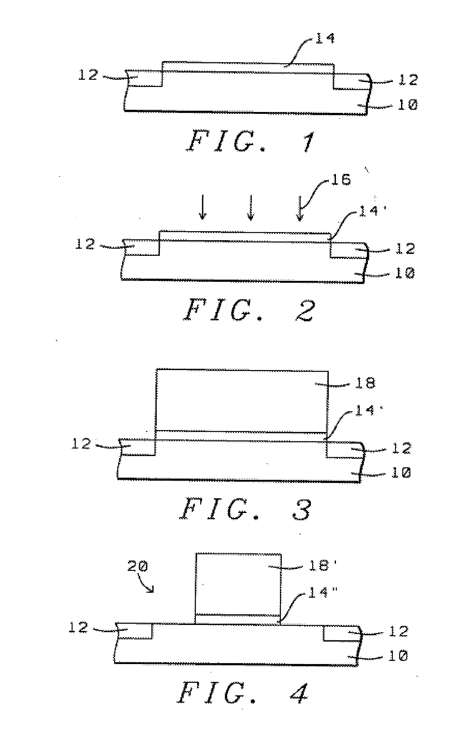
[0018] As shown in FIG. 1, structure 10 includes shallow trench isolation (STI) structures 12 formed therein. Structure 10 is preferably a silicon substrate and is understood to possibly include a semiconductor wafer or substrate. STIs 12 are comprised of thermal oxide, SACVD oxide or HDP-CVD oxide and are more preferably HDP-CVD oxide.
[0019] A high-k dielectric layer 14 is formed over silicon substrate 10 generally between STIs 12 to a thickness of preferably from about 5 to 200 .ANG. and more preferably from about 20 to 100 .ANG. . High-k dielectric layer 14 is preferably comprised of a metal oxide or a metal silicate formed by either an MOCVD process which introduces carbon (and hydrogen) impurities or an ALCVD process which introduces chlorine impurities, and does not decompose under the annealing 16 conditions of the present invention.
[0020] High-k dielectric layer 14 is preferably: (1) a metal oxide such as HfO.sub.2, ZrO.sub.2, La.sub.2O.sub.3, Y.sub.2O.sub.3, Al.sub.2O.sub.3 or TiO.sub.2 and more preferably HfO.sub.2, ZrO.sub.2 or Al.sub.2O.sub.3; or (2) a metal silicate such as HfSi.sub.xO.sub.y, ZrSi.sub.xO.sub.y, LaSi.sub.xO.sub.y, YSi.sub.xO.sub.y, AlSi.sub.xO.sub.y or TiSi.sub.xO.sub.y and more preferably HfSi.sub.xO.sub.y or ZrSi.sub.xO.sub.y.
Anneal of Deposited High-k Dielectric Layer 14--One Key Step of the Invention
[0021] In one key step of the invention and as illustrated in FIG. 2, the deposited high-k dielectric layer 14 is annealed 16 at a temperature of preferably from about 280 to 820.degree. C., more preferably from about 300 to 800.degree. C. and most preferably from about 300 to 700.degree. C. for preferably from about 0.5 to 300 seconds, more preferably from about 2 to 100 seconds for rapid thermal anneal (RTA) process and from about 5 to 300 minutes for furnace annealing processes to drive out the chlorine; and carbon and hydrogen impurities to form an impurity-free high-k dielectric layer 14'. That is the chlorine, carbon and/or hydrogen impurities are reduced to preferably less than about 20% to 2 times which improves the electrical performance of the subsequently formed transistors/devices incorporating impurity-free high-k dielectric layer 14'.
[0022] The anneal 16 is preferably by rapid thermal processing (RTP) or by a furnace anneal and is conducted so as to minimize recrystallization of the high-k dielectric layerl4. The anneal 16 is carried out in the presence of ambients that are preferably H.sub.2, N.sub.2, H.sub.2/N.sub.2, H.sub.2/O.sub.2, O.sub.2/N.sub.2, He or Ar and are more preferably H.sub.2/N.sub.2 or O.sub.2/N.sub.2. The presence of oxygen (O.sub.2) is kept low to avoid additional oxidation of the high-k dielectric layer 14.
Formation of Gate Layer 18
[0023] As shown in FIG. 3, a gate layer 18 is formed over impurity-free high-k dielectric layer 14' to a thickness of preferably from about 100 to 3000 .ANG. and more preferably from about 500 to 2000 .ANG.. Gate layer 18 is preferably comprised of polysilicon (poly) or a metal (metal gate) such as TaN/W, TiN/W, TaN/Al or TiN/Al and is more preferably polysilicon.
Further Processing
[0024] Further processing may then proceed. For example, as shown in FIG. 4, gate layer 18 and impurity-free high-k dielectric layer 14' are patterned to form gate electrode 20 comprised of patterned gate layer 18' and impurity-free high-k dielectric layer 14''.
[0025] Additional processing may continue thereafter. For example, silicide formation, LDD implants, gate sidewall spacer formation, HDD implants, etc. to complete formation of a transistor or device incorporating gate electrode 20.
Advantages of the Present Invention
[0026] The advantages of one or more embodiments of the present invention include:
[0027] 1.improved transistor/device electrical performance; and
[0028] 2.improved process for high-k film quality.
[0029] While particular embodiments of the present invention have been illustrated and described, it is not intended to limit the invention, except as defined by the following claims.
* * * * *
D00000
D00001
XML
uspto.report is an independent third-party trademark research tool that is not affiliated, endorsed, or sponsored by the United States Patent and Trademark Office (USPTO) or any other governmental organization. The information provided by uspto.report is based on publicly available data at the time of writing and is intended for informational purposes only.
While we strive to provide accurate and up-to-date information, we do not guarantee the accuracy, completeness, reliability, or suitability of the information displayed on this site. The use of this site is at your own risk. Any reliance you place on such information is therefore strictly at your own risk.
All official trademark data, including owner information, should be verified by visiting the official USPTO website at www.uspto.gov. This site is not intended to replace professional legal advice and should not be used as a substitute for consulting with a legal professional who is knowledgeable about trademark law.