Semiconductor device
Majima , et al. November 3, 2
U.S. patent number D900,759 [Application Number D/689,348] was granted by the patent office on 2020-11-03 for semiconductor device. This patent grant is currently assigned to ROHM CO., LTD.. The grantee listed for this patent is ROHM CO., LTD.. Invention is credited to Ryota Majima, Koshun Saito.


| United States Patent | D900,759 |
| Majima , et al. | November 3, 2020 |
Semiconductor device
Claims
CLAIM The ornamental design for a semiconductor device, as shown and described.
| Inventors: | Majima; Ryota (Kyoto, JP), Saito; Koshun (Kyoto, JP) | ||||||||||
|---|---|---|---|---|---|---|---|---|---|---|---|
| Applicant: |
|
||||||||||
| Assignee: | ROHM CO., LTD. (Kyoto,
JP) |
||||||||||
| Appl. No.: | D/689,348 | ||||||||||
| Filed: | April 29, 2019 |
Foreign Application Priority Data
| Nov 7, 2018 [JP] | 2018-024474 | |||
| Current U.S. Class: | D13/182 |
| Current International Class: | 1303 |
| Field of Search: | ;D10/80,103 ;D13/110,133,139,154,173,182 ;D14/217,432,433 |
References Cited [Referenced By]
U.S. Patent Documents
| D523403 | June 2006 | Mizukoshi |
| D648290 | November 2011 | Mori |
| D674760 | January 2013 | Mochizuki |
| D717254 | November 2014 | Jo |
| D729250 | May 2015 | Han |
| D777124 | January 2017 | Hasegawa |
| D783550 | April 2017 | Hasegawa |
| D796978 | September 2017 | Kawashima |
| D839220 | January 2019 | Domon |
| D845921 | April 2019 | Saito |
| D859334 | September 2019 | Yokoyama |
| D864884 | October 2019 | Yoneyama |
| 10510626 | December 2019 | Braun |
| D873227 | January 2020 | Yoneyama |
| 10546825 | January 2020 | Hsu |
| 10553559 | February 2020 | Besshi |
| 10557191 | February 2020 | Nishida |
| 10600744 | March 2020 | Chikamatsu |
| 10600789 | March 2020 | Ha |
| 10605828 | March 2020 | Kung |
| 10636703 | April 2020 | Jeong |
| 10644115 | May 2020 | Oshima |
| 10651050 | May 2020 | Nakano |
| 10672878 | June 2020 | Ohoka |
| 1162634 | Jan 2003 | JP | |||
| 1163101 | Jan 2003 | JP | |||
| 1563812 | Nov 2016 | JP | |||
Other References
|
Office Action issued for Japanese Patent Application No. 2018-024474, dated Mar. 1, 2019, 3 pages including abridged English translation. cited by applicant . "Integrated circuit device," Toshiba Semiconductor Company, Japan, JPO Publicly Known Design No. HC2000747100, date of making available to the public: Jun. 11, 2008, 5 pages including English translation of bibliographic data. cited by applicant. |
Primary Examiner: Hattan; Susan Bennett
Assistant Examiner: Tisdell; Suzanne E
Attorney, Agent or Firm: Hamre, Schumann, Mueller & Larson, P.C.
Description
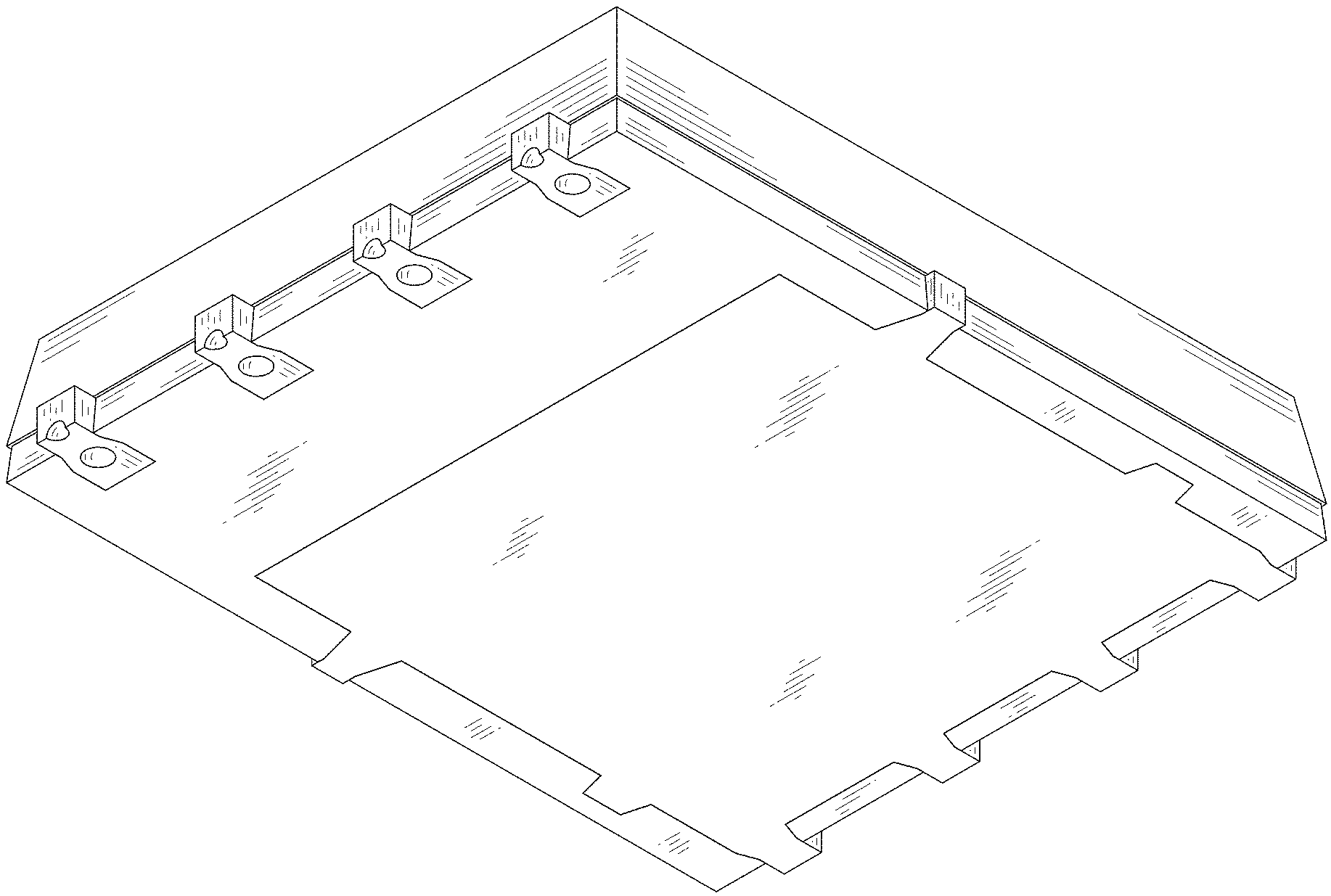
FIG. 1 is a front, bottom and right side perspective view of a semiconductor device showing our new design;
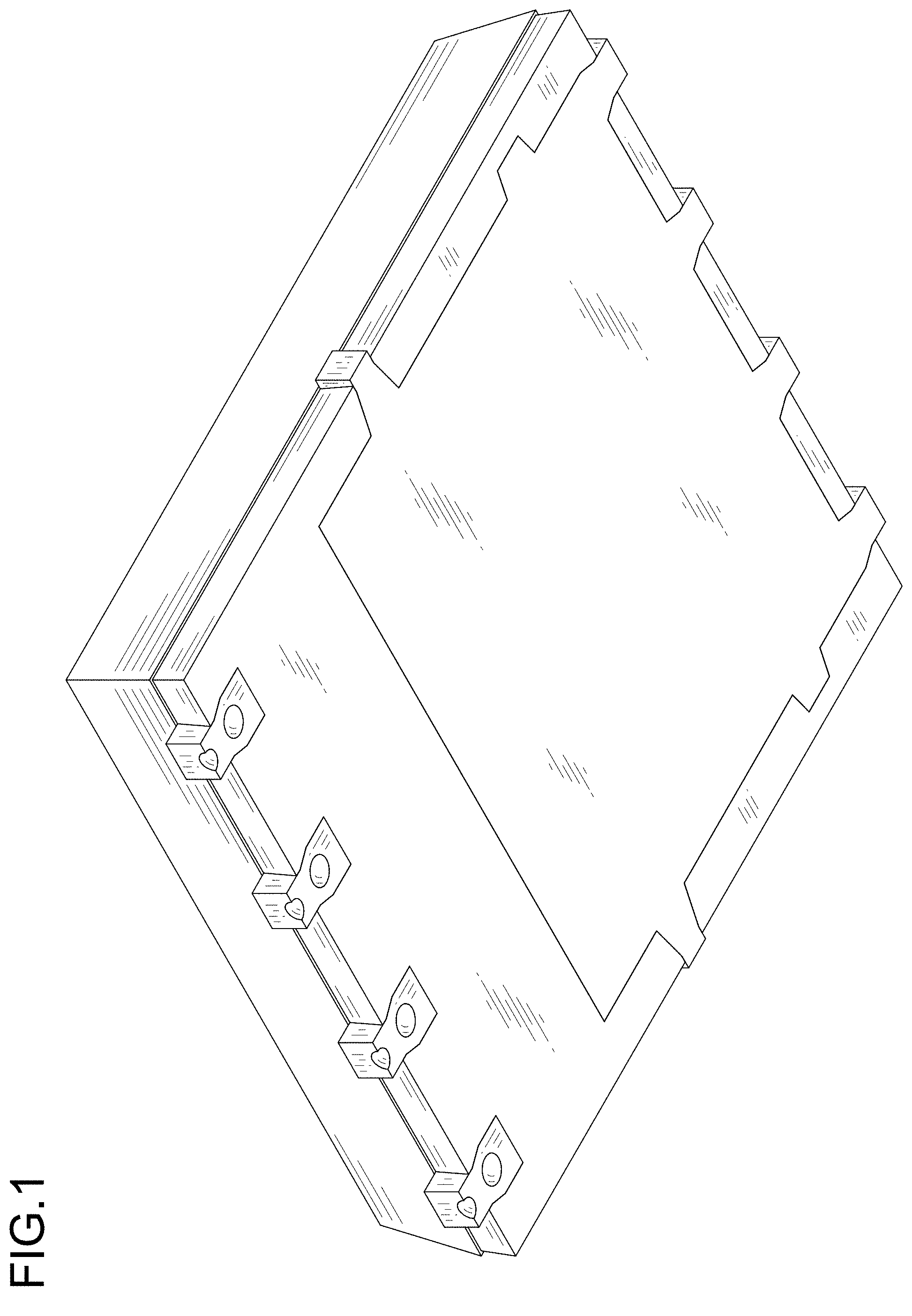
FIG. 2 is a front view thereof;
FIG. 3 is a rear view thereof;
FIG. 4 is a top plan view thereof;
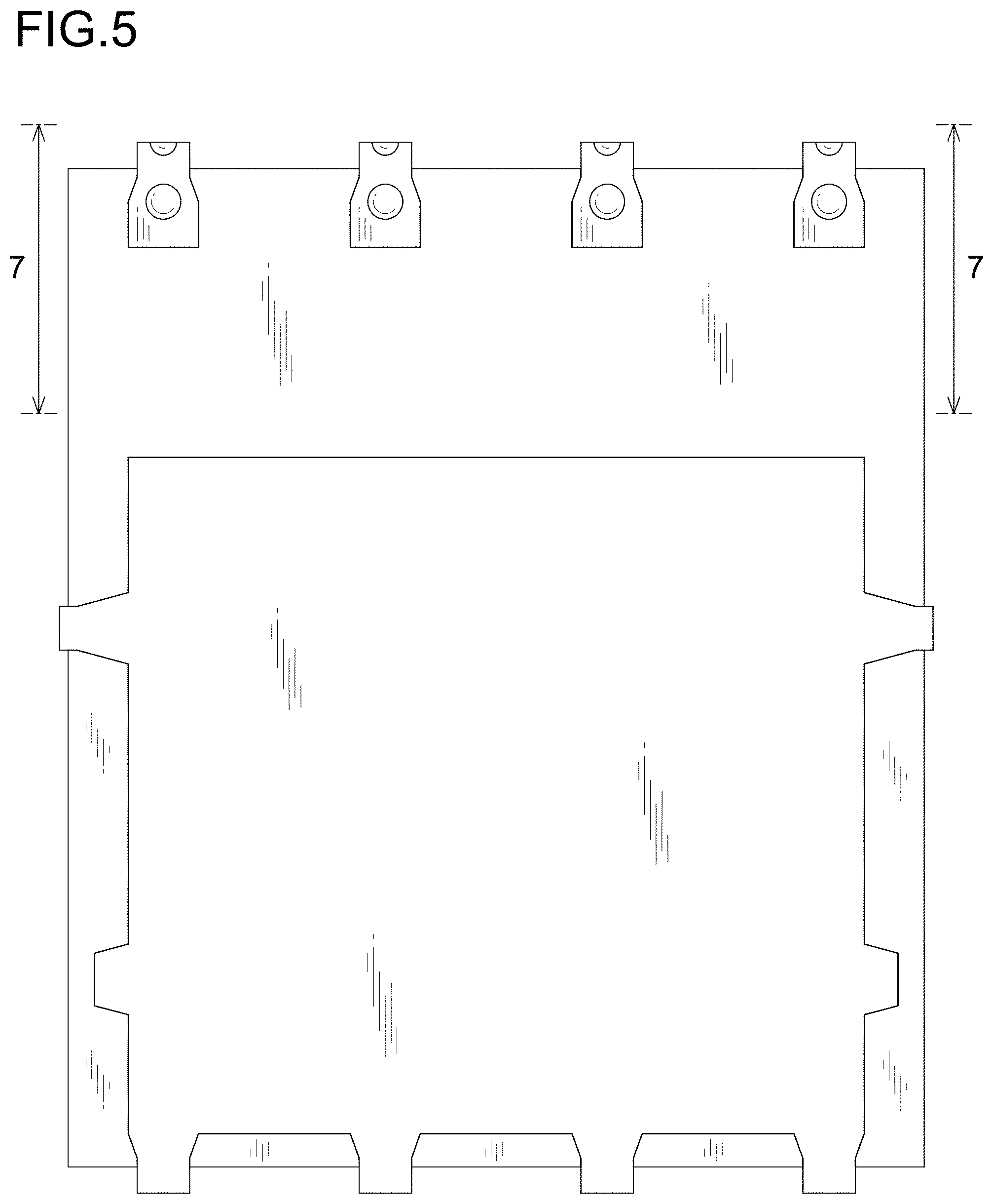
FIG. 5 is a bottom plan view thereof;
FIG. 6 is a right side view thereof, the left side view being a mirror image of FIG. 6; and,
FIG. 7 is an enlarged cross-sectional view taken along line 7-7 in FIG. 2 showing a portion indicated by lines 7-7 in FIG. 5.
* * * * *
D00000
D00001
D00002
D00003
D00004
D00005
D00006
XML
uspto.report is an independent third-party trademark research tool that is not affiliated, endorsed, or sponsored by the United States Patent and Trademark Office (USPTO) or any other governmental organization. The information provided by uspto.report is based on publicly available data at the time of writing and is intended for informational purposes only.
While we strive to provide accurate and up-to-date information, we do not guarantee the accuracy, completeness, reliability, or suitability of the information displayed on this site. The use of this site is at your own risk. Any reliance you place on such information is therefore strictly at your own risk.
All official trademark data, including owner information, should be verified by visiting the official USPTO website at www.uspto.gov. This site is not intended to replace professional legal advice and should not be used as a substitute for consulting with a legal professional who is knowledgeable about trademark law.