Semiconductor package
Itakura , et al.
U.S. patent number D877,707 [Application Number D/614,124] was granted by the patent office on 2020-03-10 for semiconductor package. This patent grant is currently assigned to Mitsubishi Electric Corporation. The grantee listed for this patent is Mitsubishi Electric Corporation. Invention is credited to Yoshihiro Akeboshi, Hiroshi Itakura, Keitaro Yamagishi.

| United States Patent | D877,707 |
| Itakura , et al. | March 10, 2020 |
Semiconductor package
Claims
CLAIM The ornamental design for a semiconductor package, as shown and described.
| Inventors: | Itakura; Hiroshi (Tokyo, JP), Yamagishi; Keitaro (Tokyo, JP), Akeboshi; Yoshihiro (Tokyo, JP) | ||||||||||
|---|---|---|---|---|---|---|---|---|---|---|---|
| Applicant: |
|
||||||||||
| Assignee: | Mitsubishi Electric Corporation
(Tokyo, JP) |
||||||||||
| Appl. No.: | D/614,124 | ||||||||||
| Filed: | August 16, 2017 |
Foreign Application Priority Data
| Mar 30, 2017 [JP] | 2017-006616 | |||
| Mar 30, 2017 [JP] | 2017-006617 | |||
| Mar 30, 2017 [JP] | 2017-006618 | |||
| Mar 30, 2017 [JP] | 2017-006619 | |||
| Mar 30, 2017 [JP] | 2017-006620 | |||
| Current U.S. Class: | D13/182 |
| Current International Class: | 1303 |
| Field of Search: | ;D13/182 ;257/678,684,690,691 ;361/679.01,713,728,736,760,761,772,775,783,820 ;174/250,253 ;438/15,25,26,51,55,63,64,106 |
References Cited [Referenced By]
U.S. Patent Documents
| 3458779 | July 1969 | Blank |
| 3562609 | February 1971 | Addamiano |
| 4267559 | May 1981 | Johnson |
| D277955 | March 1985 | Takahashi |
| D278048 | March 1985 | Takahashi |
| D278049 | March 1985 | Takahashi |
| D280812 | October 1985 | Takahashi |
| 5266817 | November 1993 | Lin |
| 5459350 | October 1995 | Date |
| 5512784 | April 1996 | Fried |
| 5564819 | October 1996 | Yamaguchi |
| D420983 | February 2000 | Choi |
| 6147367 | November 2000 | Yang |
| 6404065 | June 2002 | Choi |
| D476296 | June 2003 | Koizumi |
| D482666 | November 2003 | Kamada |
| D489695 | May 2004 | Komoto |
| D515520 | February 2006 | Komoto |
| D623546 | September 2010 | Nishikawa |
| D623547 | September 2010 | Nishikawa |
| D623548 | September 2010 | Nishikawa |
Attorney, Agent or Firm: Studebaker & Brackett PC
Description
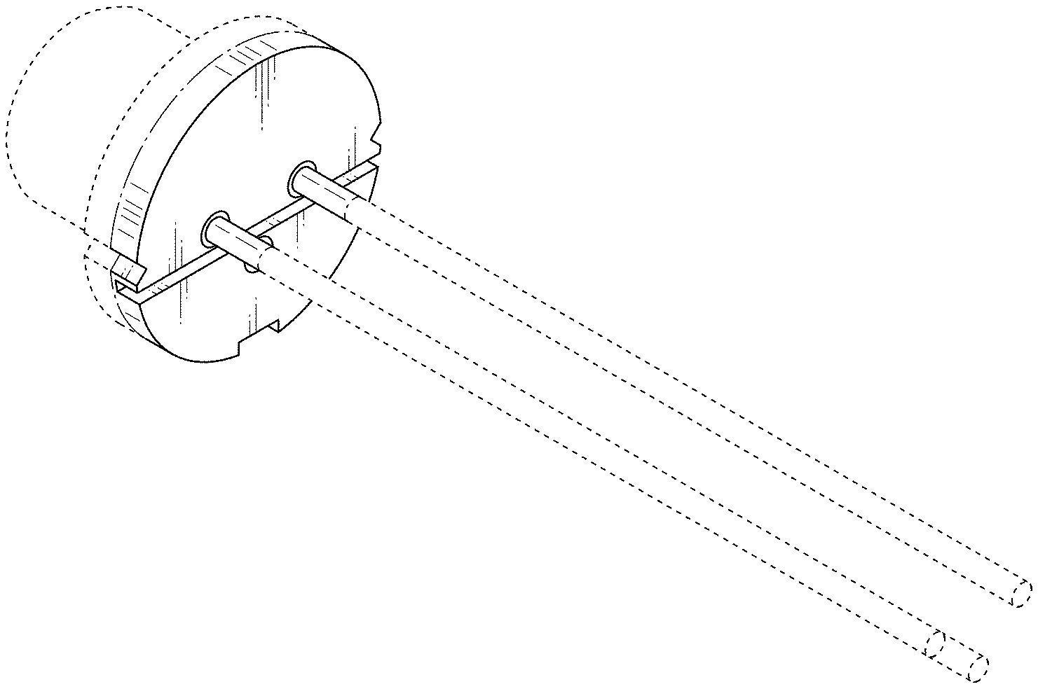
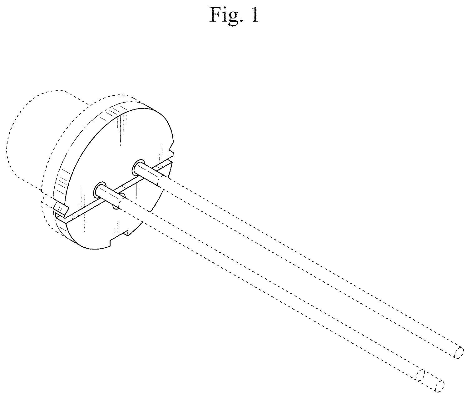
FIG. 1 is a front, top and left side perspective view of a semiconductor package showing our new design;
FIG. 2 is a front view thereof;
FIG. 3 is a rear view thereof;
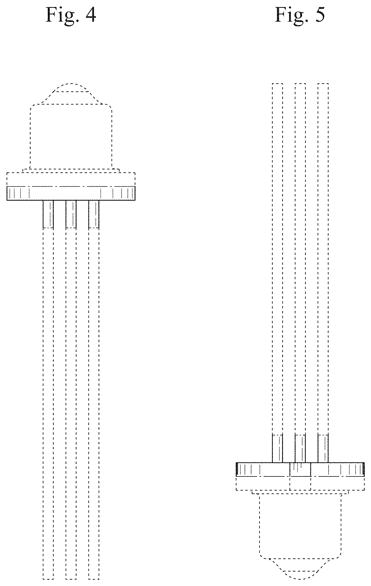
FIG. 4 is a top view thereof;
FIG. 5 is a bottom view thereof;
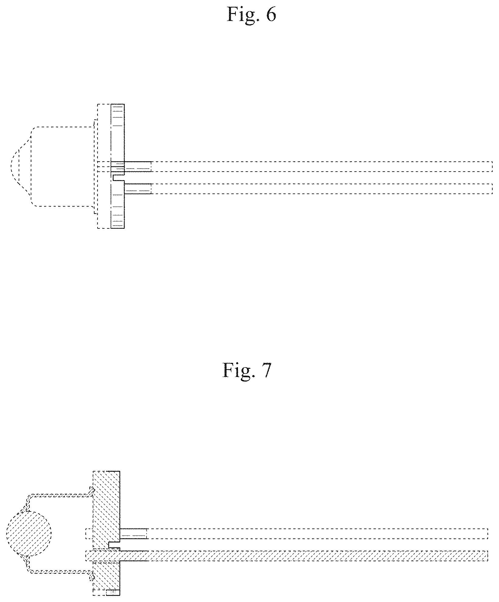
FIG. 6 is a left side view thereof; the right side view being a mirror image thereof;
FIG. 7 is a cross sectional view taken along line 7-7 of FIG. 2, with the internal system omitted; and,
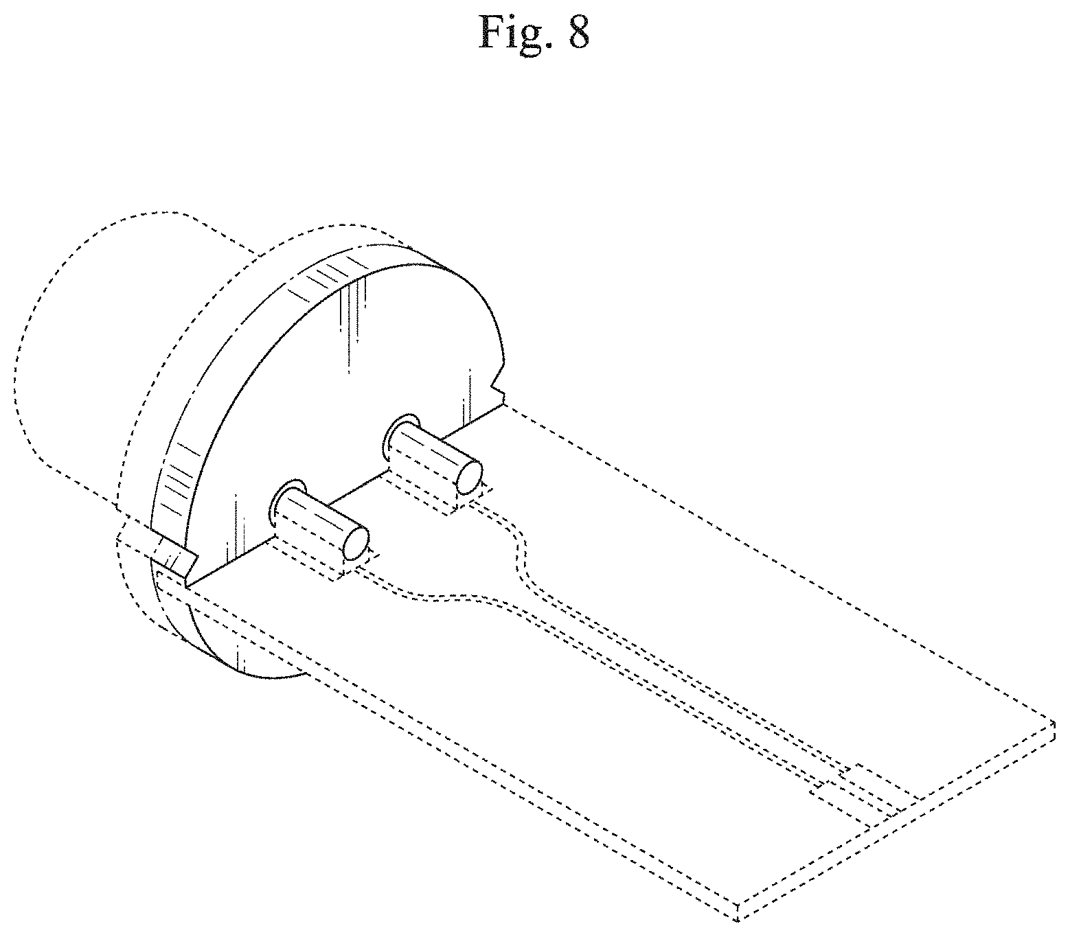
FIG. 8 is another perspective view thereof, showing the state in use.
The parts shown in even dashed broken lines do not form part of the claimed design.
* * * * *
D00000
D00001
D00002
D00003
D00004
D00005
XML
uspto.report is an independent third-party trademark research tool that is not affiliated, endorsed, or sponsored by the United States Patent and Trademark Office (USPTO) or any other governmental organization. The information provided by uspto.report is based on publicly available data at the time of writing and is intended for informational purposes only.
While we strive to provide accurate and up-to-date information, we do not guarantee the accuracy, completeness, reliability, or suitability of the information displayed on this site. The use of this site is at your own risk. Any reliance you place on such information is therefore strictly at your own risk.
All official trademark data, including owner information, should be verified by visiting the official USPTO website at www.uspto.gov. This site is not intended to replace professional legal advice and should not be used as a substitute for consulting with a legal professional who is knowledgeable about trademark law.