Acoustic resonator formed on a pedestal
Ruby December 30, 2
U.S. patent number 8,922,302 [Application Number 13/216,633] was granted by the patent office on 2014-12-30 for acoustic resonator formed on a pedestal. This patent grant is currently assigned to Avago Technologies General IP (Singapore) Pte. Ltd.. The grantee listed for this patent is Richard C. Ruby. Invention is credited to Richard C. Ruby.


View All Diagrams
| United States Patent | 8,922,302 |
| Ruby | December 30, 2014 |
Acoustic resonator formed on a pedestal
Abstract
An acoustic resonator structure comprises a substrate having a trench, a conductive pattern formed in the trench, a pillar formed within the trench, and an acoustic resonator supported at a central location by the pillar and suspended over the trench.
| Inventors: | Ruby; Richard C. (Menlo Park, CA) | ||||||||||
|---|---|---|---|---|---|---|---|---|---|---|---|
| Applicant: |
|
||||||||||
| Assignee: | Avago Technologies General IP
(Singapore) Pte. Ltd. (Singapore, SG) |
||||||||||
| Family ID: | 47017142 | ||||||||||
| Appl. No.: | 13/216,633 | ||||||||||
| Filed: | August 24, 2011 |
Prior Publication Data
| Document Identifier | Publication Date | |
|---|---|---|
| US 20130049888 A1 | Feb 28, 2013 | |
| Current U.S. Class: | 333/187; 29/594; 310/348; 29/25.35; 310/352 |
| Current CPC Class: | H03H 9/172 (20130101); H03H 3/04 (20130101); H03H 9/02133 (20130101); H03H 9/02102 (20130101); H03H 9/02047 (20130101); H03H 9/0514 (20130101); Y10T 29/4908 (20150115); Y10T 29/49005 (20150115); Y10T 29/42 (20150115) |
| Current International Class: | H03H 9/05 (20060101); H03H 9/08 (20060101); H03H 3/02 (20060101) |
| Field of Search: | ;333/187-189,133 ;310/322,334,348,349,352 ;29/25.35,594 |
References Cited [Referenced By]
U.S. Patent Documents
| 3174122 | March 1965 | Fowler et al. |
| 3189851 | June 1965 | Fowler |
| 3321648 | May 1967 | Kolm |
| 3422371 | January 1969 | Poirier et al. |
| 3568108 | March 1971 | Poirier et al. |
| 3582839 | June 1971 | Pim et al. |
| 3590287 | June 1971 | Berlincourt et al. |
| 3610969 | October 1971 | Clawson et al. |
| 3826931 | July 1974 | Hammond |
| 3845402 | October 1974 | Nupp |
| 4084217 | April 1978 | Brandli et al. |
| 4172277 | October 1979 | Pinson |
| 4272742 | June 1981 | Lewis |
| 4281299 | July 1981 | Newbold |
| 4320365 | March 1982 | Black et al. |
| 4344004 | August 1982 | Okubo |
| 4355408 | October 1982 | Scarrott |
| 4456850 | June 1984 | Inoue et al. |
| 4529904 | July 1985 | Hattersley |
| 4608541 | August 1986 | Moriwaki et al. |
| 4625138 | November 1986 | Ballato |
| 4640756 | February 1987 | Wang et al. |
| 4719383 | January 1988 | Wang et al. |
| 4769272 | September 1988 | Byrne et al. |
| 4798990 | January 1989 | Henoch |
| 4819215 | April 1989 | Yokoyama et al. |
| 4836882 | June 1989 | Ballato |
| 4841429 | June 1989 | McClanahan et al. |
| 4906840 | March 1990 | Zdeblick et al. |
| 5048036 | September 1991 | Scifres et al. |
| 5048038 | September 1991 | Brennan et al. |
| 5066925 | November 1991 | Freitag |
| 5075641 | December 1991 | Weber et al. |
| 5111157 | May 1992 | Komiak |
| 5118982 | June 1992 | Inoue et al. |
| 5129132 | July 1992 | Zdeblick et al. |
| 5162691 | November 1992 | Mariani et al. |
| 5166646 | November 1992 | Avanic et al. |
| 5185589 | February 1993 | Krishnaswamy et al. |
| 5214392 | May 1993 | Kobayashi et al. |
| 5233259 | August 1993 | Krishnaswamy et al. |
| 5241209 | August 1993 | Sasaki |
| 5241456 | August 1993 | Marcinkiewicz et al. |
| 5260596 | November 1993 | Dunn et al. |
| 5262347 | November 1993 | Sands |
| 5270492 | December 1993 | Fukui |
| 5294898 | March 1994 | Dworsky et al. |
| 5361077 | November 1994 | Weber |
| 5382930 | January 1995 | Stokes et al. |
| 5384808 | January 1995 | Van Brunt et al. |
| 5448014 | September 1995 | Kong et al. |
| 5465725 | November 1995 | Seyed-Bolorforosh |
| 5475351 | December 1995 | Uematsu et al. |
| 5548189 | August 1996 | Williams |
| 5587620 | December 1996 | Ruby et al. |
| 5589858 | December 1996 | Kadowaki et al. |
| 5594705 | January 1997 | Connor et al. |
| 5603324 | February 1997 | Oppelt et al. |
| 5633574 | May 1997 | Sage |
| 5671242 | September 1997 | Takiguchi et al. |
| 5692279 | December 1997 | Mang et al. |
| 5704037 | December 1997 | Chen |
| 5705877 | January 1998 | Shimada |
| 5714917 | February 1998 | Ella |
| 5729008 | March 1998 | Blalock et al. |
| 5789845 | August 1998 | Wadaka et al. |
| 5835142 | November 1998 | Nakamura et al. |
| 5853601 | December 1998 | Krishaswamy et al. |
| 5864261 | January 1999 | Weber |
| 5866969 | February 1999 | Shimada et al. |
| 5872493 | February 1999 | Ella |
| 5873153 | February 1999 | Ruby et al. |
| 5873154 | February 1999 | Ylilammi et al. |
| 5894184 | April 1999 | Furuhashi et al. |
| 5894647 | April 1999 | Lakin |
| 5910756 | June 1999 | Ella |
| 5917272 | June 1999 | Clark et al. |
| 5932953 | August 1999 | Drees et al. |
| 5936150 | August 1999 | Kobrin et al. |
| 5953479 | September 1999 | Zhou et al. |
| 5955926 | September 1999 | Uda et al. |
| 5962787 | October 1999 | Okada et al. |
| 5969463 | October 1999 | Tomita et al. |
| 5977840 | November 1999 | Connell et al. |
| 5982297 | November 1999 | Welle |
| 6001664 | December 1999 | Swirhun et al. |
| 6016052 | January 2000 | Vaughn |
| 6040962 | March 2000 | Kanazawa et al. |
| 6051907 | April 2000 | Ylilammi |
| 6060818 | May 2000 | Ruby et al. |
| 6087198 | July 2000 | Panasik |
| 6090687 | July 2000 | Merchant et al. |
| 6107721 | August 2000 | Lakin |
| 6111338 | August 2000 | Otsuchi et al. |
| 6111341 | August 2000 | Hirama |
| 6111480 | August 2000 | Iyama et al. |
| 6118181 | September 2000 | Merchant et al. |
| 6124678 | September 2000 | Bishop et al. |
| 6124756 | September 2000 | Yaklin et al. |
| 6131256 | October 2000 | Dydyk |
| 6150703 | November 2000 | Cushman et al. |
| 6187513 | February 2001 | Katakura |
| 6196059 | March 2001 | Koesslinger |
| 6198208 | March 2001 | Yano et al. |
| 6215375 | April 2001 | Larson, III et al. |
| 6219032 | April 2001 | Rosenberg et al. |
| 6219263 | April 2001 | Wuidart |
| 6228675 | May 2001 | Ruby et al. |
| 6229247 | May 2001 | Bishop |
| 6252229 | June 2001 | Hays et al. |
| 6262600 | July 2001 | Haigh et al. |
| 6262637 | July 2001 | Bradley et al. |
| 6263735 | July 2001 | Nakatani et al. |
| 6265246 | July 2001 | Ruby et al. |
| 6278342 | August 2001 | Ella |
| 6292336 | September 2001 | Horng et al. |
| 6307447 | October 2001 | Barber et al. |
| 6307761 | October 2001 | Nakagawa |
| 6335548 | January 2002 | Roberts et al. |
| 6355498 | March 2002 | Chan et al. |
| 6366006 | April 2002 | Boyd |
| 6376280 | April 2002 | Ruby et al. |
| 6377137 | April 2002 | Ruby |
| 6384679 | May 2002 | Lorenz |
| 6384697 | May 2002 | Ruby |
| 6396200 | May 2002 | Misu et al. |
| 6407649 | June 2002 | Tikka et al. |
| 6414569 | July 2002 | Nakafuku |
| 6420820 | July 2002 | Larson, III |
| 6424237 | July 2002 | Ruby et al. |
| 6429511 | August 2002 | Ruby et al. |
| 6434030 | August 2002 | Rehm et al. |
| 6437482 | August 2002 | Shibata |
| 6437484 | August 2002 | Nishimura et al. |
| 6441539 | August 2002 | Kitamura et al. |
| 6441702 | August 2002 | Ella et al. |
| 6462631 | October 2002 | Bradley et al. |
| 6466105 | October 2002 | Lobl et al. |
| 6466418 | October 2002 | Horng et al. |
| 6469597 | October 2002 | Ruby et al. |
| 6469909 | October 2002 | Simmons |
| 6472954 | October 2002 | Ruby et al. |
| 6476536 | November 2002 | Pensala |
| 6479320 | November 2002 | Gooch |
| 6483229 | November 2002 | Larson, III et al. |
| 6486751 | November 2002 | Barber et al. |
| 6489688 | December 2002 | Baumann et al. |
| 6492883 | December 2002 | Liang et al. |
| 6496085 | December 2002 | Ella et al. |
| 6498604 | December 2002 | Jensen |
| 6507983 | January 2003 | Ruby et al. |
| 6509813 | January 2003 | Ella et al. |
| 6515558 | February 2003 | Ylilammi |
| 6518860 | February 2003 | Ella et al. |
| 6525996 | February 2003 | Miyazawa |
| 6528344 | March 2003 | Kang |
| 6530515 | March 2003 | Glenn et al. |
| 6534900 | March 2003 | Aigner et al. |
| 6542054 | April 2003 | Aigner et al. |
| 6542055 | April 2003 | Frank et al. |
| 6548942 | April 2003 | Panasik |
| 6548943 | April 2003 | Kaitila et al. |
| 6549394 | April 2003 | Williams |
| 6550664 | April 2003 | Bradley et al. |
| 6559487 | May 2003 | Kang et al. |
| 6559530 | May 2003 | Hinzel et al. |
| 6564448 | May 2003 | Oura et al. |
| 6566956 | May 2003 | Ohnishi et al. |
| 6566979 | May 2003 | Larson, III et al. |
| 6580159 | June 2003 | Fusaro et al. |
| 6583374 | June 2003 | Knieser et al. |
| 6583688 | June 2003 | Klee et al. |
| 6593870 | July 2003 | Dummermuth et al. |
| 6594165 | July 2003 | Duerbaum et al. |
| 6600390 | July 2003 | Frank |
| 6601276 | August 2003 | Barber |
| 6603182 | August 2003 | Low et al. |
| 6617249 | September 2003 | Ruby et al. |
| 6617750 | September 2003 | Dummermuth et al. |
| 6617751 | September 2003 | Sunwoo et al. |
| 6621137 | September 2003 | Ma et al. |
| 6630753 | October 2003 | Malik et al. |
| 6635509 | October 2003 | Ouellet |
| 6635519 | October 2003 | Barber et al. |
| 6639872 | October 2003 | Rein |
| 6650205 | November 2003 | Goetz et al. |
| 6651488 | November 2003 | Larson, III et al. |
| 6657363 | December 2003 | Aigner |
| 6668618 | December 2003 | Larson, III et al. |
| 6670866 | December 2003 | Ella et al. |
| 6693500 | February 2004 | Yang et al. |
| 6710508 | March 2004 | Ruby et al. |
| 6710681 | March 2004 | Figueredo et al. |
| 6713314 | March 2004 | Wong et al. |
| 6714102 | March 2004 | Ruby et al. |
| 6720844 | April 2004 | Lakin |
| 6720846 | April 2004 | Iwashita et al. |
| 6724266 | April 2004 | Piazza et al. |
| 6738267 | May 2004 | Navas Sabater et al. |
| 6762471 | July 2004 | Kim |
| 6774746 | August 2004 | Whatmore et al. |
| 6777263 | August 2004 | Gan et al. |
| 6787048 | September 2004 | Bradley et al. |
| 6787897 | September 2004 | Geefay et al. |
| 6788170 | September 2004 | Kaitila et al. |
| 6803835 | October 2004 | Frank |
| 6812619 | November 2004 | Kaitila et al. |
| 6828713 | December 2004 | Bradley et al. |
| 6842088 | January 2005 | Yamada et al. |
| 6842089 | January 2005 | Lee |
| 6853534 | February 2005 | Williams |
| 6861920 | March 2005 | Ishikawa et al. |
| 6873065 | March 2005 | Haigh et al. |
| 6873529 | March 2005 | Ikuta et al. |
| 6874211 | April 2005 | Bradley et al. |
| 6874212 | April 2005 | Larson, III |
| 6888424 | May 2005 | Takeuchi et al. |
| 6894360 | May 2005 | Bradley |
| 6894588 | May 2005 | Detlefsen |
| 6900705 | May 2005 | Nakamura et al. |
| 6903452 | June 2005 | Ma et al. |
| 6906451 | June 2005 | Yamada et al. |
| 6911708 | June 2005 | Park |
| 6917261 | July 2005 | Unterberger |
| 6919222 | July 2005 | Geefay |
| 6924583 | August 2005 | Lin et al. |
| 6924717 | August 2005 | Ginsburg et al. |
| 6927651 | August 2005 | Larson, III et al. |
| 6933809 | August 2005 | Kyoung et al. |
| 6936928 | August 2005 | Hedler et al. |
| 6936954 | August 2005 | Peczalski |
| 6943647 | September 2005 | Aigner |
| 6943648 | September 2005 | Maiz et al. |
| 6946928 | September 2005 | Larson, III et al. |
| 6954121 | October 2005 | Bradley et al. |
| 6963257 | November 2005 | Ella et al. |
| 6970365 | November 2005 | Turchi |
| 6975183 | December 2005 | Aigner et al. |
| 6977563 | December 2005 | Komuro et al. |
| 6979597 | December 2005 | Geefay et al. |
| 6985052 | January 2006 | Tikka |
| 6987433 | January 2006 | Larson, III et al. |
| 6989723 | January 2006 | Komuro et al. |
| 6998940 | February 2006 | Metzger |
| 7002437 | February 2006 | Takeuchi et al. |
| 7019604 | March 2006 | Gotoh et al. |
| 7019605 | March 2006 | Larson, III |
| 7026876 | April 2006 | Esfandiari et al. |
| 7053456 | May 2006 | Matsuo |
| 7057476 | June 2006 | Hwu |
| 7057478 | June 2006 | Korden et al. |
| 7064606 | June 2006 | Louis |
| 7084553 | August 2006 | Ludwiczak |
| 7091649 | August 2006 | Larson, III et al. |
| 7098758 | August 2006 | Wang et al. |
| 7102460 | September 2006 | Schmidhammer et al. |
| 7128941 | October 2006 | Lee |
| 7129806 | October 2006 | Sato |
| 7138889 | November 2006 | Lakin |
| 7161283 | January 2007 | Geefay |
| 7161448 | January 2007 | Feng et al. |
| 7170215 | January 2007 | Namba et al. |
| 7173504 | February 2007 | Larson, III et al. |
| 7187254 | March 2007 | Su et al. |
| 7209374 | April 2007 | Noro |
| 7212083 | May 2007 | Inoue et al. |
| 7212085 | May 2007 | Wu |
| 7221242 | May 2007 | Asai |
| 7230509 | June 2007 | Stoemmer |
| 7230511 | June 2007 | Onishi et al. |
| 7235462 | June 2007 | Letertre et al. |
| 7242270 | July 2007 | Larson, III et al. |
| 7259498 | August 2007 | Nakatsuka et al. |
| 7268647 | September 2007 | Sano et al. |
| 7275292 | October 2007 | Ruby et al. |
| 7276994 | October 2007 | Takeuchi et al. |
| 7280007 | October 2007 | Feng et al. |
| 7281304 | October 2007 | Kim et al. |
| 7294919 | November 2007 | Bai |
| 7301258 | November 2007 | Tanaka |
| 7310861 | December 2007 | Aigner et al. |
| 7312675 | December 2007 | Ruby et al. |
| 7332985 | February 2008 | Larson, III et al. |
| 7345409 | March 2008 | Leidl et al. |
| 7345410 | March 2008 | Grannen et al. |
| 7358831 | April 2008 | Larson et al. |
| 7367095 | May 2008 | Larson, III et al. |
| 7368857 | May 2008 | Tanaka |
| 7369013 | May 2008 | Fazzio et al. |
| 7382078 | June 2008 | Bradley |
| 7385467 | June 2008 | Stoemmer et al. |
| 7388318 | June 2008 | Yamada et al. |
| 7388454 | June 2008 | Ruby et al. |
| 7388455 | June 2008 | Larson, III |
| 7408428 | August 2008 | Larson, III |
| 7414349 | August 2008 | Sasaki |
| 7414495 | August 2008 | Iwasaki et al. |
| 7423503 | September 2008 | Larson, III et al. |
| 7425787 | September 2008 | Larson, III |
| 7439824 | October 2008 | Aigner |
| 7563475 | July 2009 | Ruby et al. |
| 7619493 | November 2009 | Uno et al. |
| 7623007 | November 2009 | Nakatsuka et al. |
| 7629865 | December 2009 | Ruby |
| 7714684 | May 2010 | Ruby et al. |
| 7791434 | September 2010 | Fazzio et al. |
| 7889024 | February 2011 | Bradley et al. |
| 7986075 | July 2011 | Asai et al. |
| 8188810 | May 2012 | Fazzio et al. |
| 8248185 | August 2012 | Choy et al. |
| 2001/0028285 | October 2001 | Klee et al. |
| 2002/0000646 | January 2002 | Gooch et al. |
| 2002/0030424 | March 2002 | Iwata |
| 2002/0063497 | May 2002 | Panasik |
| 2002/0070463 | June 2002 | Chang et al. |
| 2002/0109565 | August 2002 | Ella et al. |
| 2002/0121944 | September 2002 | Larson, III et al. |
| 2002/0121945 | September 2002 | Ruby et al. |
| 2002/0126517 | September 2002 | Matsukawa et al. |
| 2002/0140520 | October 2002 | Hikita et al. |
| 2002/0152803 | October 2002 | Larson, III et al. |
| 2002/0158702 | October 2002 | Tikka et al. |
| 2002/0158714 | October 2002 | Kaitila |
| 2002/0190814 | December 2002 | Yamada et al. |
| 2003/0001251 | January 2003 | Cheever et al. |
| 2003/0006502 | January 2003 | Karpman |
| 2003/0011285 | January 2003 | Ossmann |
| 2003/0011446 | January 2003 | Bradley |
| 2003/0051550 | March 2003 | Nguyen et al. |
| 2003/0087469 | May 2003 | Ma |
| 2003/0102776 | June 2003 | Takeda et al. |
| 2003/0111439 | June 2003 | Fetter et al. |
| 2003/0128081 | July 2003 | Ella et al. |
| 2003/0132493 | July 2003 | Kang et al. |
| 2003/0132809 | July 2003 | Senthilkumar et al. |
| 2003/0141946 | July 2003 | Ruby et al. |
| 2003/0179053 | September 2003 | Aigner et al. |
| 2003/0205948 | November 2003 | Lin et al. |
| 2003/0213964 | November 2003 | Flynn et al. |
| 2004/0016995 | January 2004 | Kuo et al. |
| 2004/0017130 | January 2004 | Wang et al. |
| 2004/0056735 | March 2004 | Nomura et al. |
| 2004/0092234 | May 2004 | Pohjonen |
| 2004/0099898 | May 2004 | Grivna et al. |
| 2004/0124952 | July 2004 | Tikka |
| 2004/0129079 | July 2004 | Kato et al. |
| 2004/0150293 | August 2004 | Unterberger |
| 2004/0150296 | August 2004 | Park et al. |
| 2004/0166603 | August 2004 | Carley |
| 2004/0188241 | September 2004 | Rich et al. |
| 2004/0195937 | October 2004 | Matsubara et al. |
| 2004/0212458 | October 2004 | Lee |
| 2004/0257171 | December 2004 | Park et al. |
| 2004/0257172 | December 2004 | Schmidhammer et al. |
| 2004/0263287 | December 2004 | Ginsburg et al. |
| 2005/0012570 | January 2005 | Korden et al. |
| 2005/0012571 | January 2005 | Song et al. |
| 2005/0012716 | January 2005 | Mikulin et al. |
| 2005/0023931 | February 2005 | Bouche et al. |
| 2005/0023932 | February 2005 | Inoue et al. |
| 2005/0030126 | February 2005 | Inoue et al. |
| 2005/0036604 | February 2005 | Scott et al. |
| 2005/0057117 | March 2005 | Nakatsuka et al. |
| 2005/0057324 | March 2005 | Onishi et al. |
| 2005/0068124 | March 2005 | Stoemmer |
| 2005/0093396 | May 2005 | Larson, III et al. |
| 2005/0093399 | May 2005 | Inoue |
| 2005/0093653 | May 2005 | Larson, III |
| 2005/0093654 | May 2005 | Larson, III et al. |
| 2005/0093655 | May 2005 | Larson, III et al. |
| 2005/0093657 | May 2005 | Larson, III et al. |
| 2005/0093658 | May 2005 | Larson, III et al. |
| 2005/0093659 | May 2005 | Larson, III et al. |
| 2005/0104690 | May 2005 | Larson, III et al. |
| 2005/0110598 | May 2005 | Larson, III |
| 2005/0128030 | June 2005 | Larson, III et al. |
| 2005/0140466 | June 2005 | Larson, III et al. |
| 2005/0167795 | August 2005 | Higashi |
| 2005/0193507 | September 2005 | Ludwiczak |
| 2005/0206271 | September 2005 | Higuchi et al. |
| 2005/0206483 | September 2005 | Pashby et al. |
| 2005/0218488 | October 2005 | Matsuo |
| 2005/0269904 | December 2005 | Oka |
| 2005/0275486 | December 2005 | Feng |
| 2006/0017352 | January 2006 | Tanielian |
| 2006/0071736 | April 2006 | Ruby et al. |
| 2006/0081048 | April 2006 | Mikado et al. |
| 2006/0087199 | April 2006 | Larson, III et al. |
| 2006/0103492 | May 2006 | Feng et al. |
| 2006/0119453 | June 2006 | Fattinger et al. |
| 2006/0125489 | June 2006 | Feucht et al. |
| 2006/0132262 | June 2006 | Fazzio et al. |
| 2006/0164183 | July 2006 | Tikka et al. |
| 2006/0185139 | August 2006 | Larson, III et al. |
| 2006/0197411 | September 2006 | Hoen et al. |
| 2006/0238070 | October 2006 | Costa et al. |
| 2006/0284707 | December 2006 | Larson, III et al. |
| 2006/0290446 | December 2006 | Aigner et al. |
| 2007/0035214 | February 2007 | Kasahara |
| 2007/0037311 | February 2007 | Izumi et al. |
| 2007/0040473 | February 2007 | Ballandras et al. |
| 2007/0069225 | March 2007 | Krames et al. |
| 2007/0069606 | March 2007 | Matsumoto et al. |
| 2007/0080759 | April 2007 | Jamneala et al. |
| 2007/0085447 | April 2007 | Larson, III |
| 2007/0085631 | April 2007 | Larson, III et al. |
| 2007/0085632 | April 2007 | Larson, III et al. |
| 2007/0086080 | April 2007 | Larson, III et al. |
| 2007/0086274 | April 2007 | Nishimura et al. |
| 2007/0090892 | April 2007 | Larson, III |
| 2007/0170815 | July 2007 | Unkrich |
| 2007/0171002 | July 2007 | Unkrich |
| 2007/0176710 | August 2007 | Jamneala et al. |
| 2007/0205850 | September 2007 | Jamneala et al. |
| 2007/0228876 | October 2007 | Sung |
| 2007/0266548 | November 2007 | Fattinger |
| 2007/0279153 | December 2007 | Ruby |
| 2008/0055020 | March 2008 | Handtmann et al. |
| 2008/0111651 | May 2008 | Isobe et al. |
| 2008/0258842 | October 2008 | Ruby et al. |
| 2008/0283944 | November 2008 | Geefay |
| 2008/0297279 | December 2008 | Thalhammer et al. |
| 2008/0297280 | December 2008 | Thalhammer et al. |
| 2008/0309432 | December 2008 | Fattinger et al. |
| 2009/0267457 | October 2009 | Barber et al. |
| 2010/0111808 | May 2010 | Pimputkar et al. |
| 2010/0176899 | July 2010 | Schaufele et al. |
| 2010/0187948 | July 2010 | Sinha et al. |
| 2010/0327697 | December 2010 | Choy et al. |
| 2010/0327994 | December 2010 | Choy et al. |
| 2011/0180391 | July 2011 | Larson et al. |
| 2012/0177816 | July 2012 | Larson et al. |
| 2012/0326807 | December 2012 | Choy et al. |
| 2013/0049888 | February 2013 | Ruby |
| 2013/0194057 | August 2013 | Ruby |
| 10160617 | Jun 2003 | DE | |||
| 231892 | Aug 1987 | EP | |||
| 0637875 | Feb 1995 | EP | |||
| 689254 | Dec 1995 | EP | |||
| 0865157 | Sep 1998 | EP | |||
| 880227 | Nov 1998 | EP | |||
| 1047189 | Oct 2000 | EP | |||
| 1096259 | May 2001 | EP | |||
| 1100196 | May 2001 | EP | |||
| 1180494 | Feb 2002 | EP | |||
| 1249932 | Oct 2002 | EP | |||
| 1258989 | Nov 2002 | EP | |||
| 1258990 | Nov 2002 | EP | |||
| 1517443 | Mar 2005 | EP | |||
| 1517444 | Mar 2005 | EP | |||
| 1528674 | May 2005 | EP | |||
| 1528675 | May 2005 | EP | |||
| 1528676 | May 2005 | EP | |||
| 1528677 | May 2005 | EP | |||
| 1542362 | Jun 2005 | EP | |||
| 1557945 | Jul 2005 | EP | |||
| 1575165 | Sep 2005 | EP | |||
| 0973256 | Sep 2006 | EP | |||
| 2299593 | Mar 2011 | EP | |||
| 1207974 | Oct 1970 | GB | |||
| 2013343 | Aug 1979 | GB | |||
| 2411239 | Aug 2005 | GB | |||
| 2418791 | Apr 2006 | GB | |||
| 2427773 | Jan 2007 | GB | |||
| 61054686 | Mar 1986 | JP | |||
| 62-200813 | Sep 1987 | JP | |||
| 1-295512 | Nov 1989 | JP | |||
| 2-10907 | Jan 1990 | JP | |||
| 06005944 | Jan 1994 | JP | |||
| 8-330878 | Dec 1996 | JP | |||
| 9-83029 | Mar 1997 | JP | |||
| 10-32456 | Feb 1998 | JP | |||
| 2000-31552 | Jan 2000 | JP | |||
| 2000-232334 | Aug 2000 | JP | |||
| 2001-102901 | Apr 2001 | JP | |||
| 2001-508630 | Jun 2001 | JP | |||
| 2002/217676 | Aug 2002 | JP | |||
| 2003/124779 | Apr 2003 | JP | |||
| WO-98/16957 | Apr 1998 | WO | |||
| WO-98/56049 | Dec 1998 | WO | |||
| WO-01/06646 | Jan 2001 | WO | |||
| WO-01/06647 | Jan 2001 | WO | |||
| WO-0199276 | Dec 2001 | WO | |||
| WO-02/103900 | Dec 2002 | WO | |||
| WO-03/030358 | Apr 2003 | WO | |||
| WO-03/043188 | May 2003 | WO | |||
| WO-03/050950 | Jun 2003 | WO | |||
| WO-03/058809 | Jul 2003 | WO | |||
| WO-2004/034579 | Apr 2004 | WO | |||
| WO-2004/051744 | Jun 2004 | WO | |||
| WO-2004/102688 | Nov 2004 | WO | |||
| WO-2005/043752 | May 2005 | WO | |||
| WO-2005/043753 | May 2005 | WO | |||
| WO-2005/043756 | May 2005 | WO | |||
| WO-2006/018788 | Feb 2006 | WO | |||
Other References
|
Co-pending U.S. Appl. No. 12/891,039, filed Sep. 27, 2010. cited by applicant . Co-pending U.S. Appl. No. 13/162,883, filed Jun. 17, 2011. cited by applicant . U.S. Appl. No. 10/971,169, filed Oct. 22, 2004, Larson III, John D., et al. cited by applicant . Al-Ahmad, M. et al., "Piezoelectric-Based Tunable Microstrip Shunt Resonator", Proceedings of Asia-Pacific Microwave Conference 2006. cited by applicant . Ambacher, , "Growth and Applications of Group III-Nitrides", J. Phys. D: Appl. Phys. 31 1998, 2653-2710. cited by applicant . Aoyama, Takayuki at al., "Diffusion of Boron, Phosphorous, Arsenic and Antimony in Thermally Grown SiliconDioxide", Journal of the Electrochemical Society, vol. 146, No. 5 1999, 1879-1883. cited by applicant . Auld, B. A. , "Acoustic Resonators", Acoustic Fields and Waves in Solids, Second Edition, vol. II 1990, 250-259. cited by applicant . Bauer, L. O. et al., "Properties of Silicon Implanted with Boron Ions through Thermal Silicon Dioxide", Solid State Electronics, vol. 16, No. 3 Mar. 1973, 289-300. cited by applicant . Choi, Sungjin et al., "Design of Half-Bridge Piezo-Transformer Converters in the AC Adapter Applications", APEC 2005, IEEE Mar. 2005, 244-248. cited by applicant . Coombs, Clyde F., "Electronic Instrument Handbook", Second Edition, McGraw-Hill, Inc. 1995, pp. 5.1 to 5.29. cited by applicant . Dalmau, R. et al., "A1N Bulk Crystals Grown on CiC seeds", Journal of Crystal Growth 281 2005, 68-74. cited by applicant . Fattinger, G. G. et al., "Coupled Bulk Acoustic Wave Resonator Filters: Key technology for single-to-balanced RF filters", 0-7803-8331-1/4/W20.00; IEEE MTT-S Digest 2004, 927-929. cited by applicant . Hadimioglu, B. et al., "Polymer Films As Acoustic Matching Layers"., 1990 IEEE Ultrasonics Symposium Proceedings, vol. 3 pp. [Previously submitted as "Polymer Files As Acoustic Matching Layers, 1990 IEEE Ultrasonics Symposium Proceeding. vol. 4 pp. 1227-1340, Dec. 1990". Considered by Examiner on Mar. 20, 2007 Dec. 1990, 1337-1340. cited by applicant . Hara, K. , "Surface Treatment of Quartz Oscillator Plate by Ion Implantation", Oyo Buturi, vol. 47, No. Feb. 2, 1978 , 145-146. cited by applicant . Holzlohner, Ronald et al., "Accurate Calculation of Eye Diagrams and Bit Error Rates in Optical Transmission Systems Using Linearization", Journal of Lightwave Technology, vol. 20, No. 3, Mar. 2002, pp. 389-400. cited by applicant . Ivensky, Gregory et al., "A Comparison of Piezoelectric Transformer AC/DC Converters with Current Doubler and voltage Doubler Rectifiers", IEEE Transactions on Power Electronics, vol. 19, No. 6. Nov. 2004. cited by applicant . Jiang, Yimin et al., "A Novel Single-Phase Power Factor Correction Scheme", IEEE 1993 , 287-292. cited by applicant . Jung, Jun-Phil et al., "Experimental and Theoretical Investigation on the Relationship Between AIN Properties and AIN-Based FBAR Characteristics", 2003 IEEE International. Frequency Control Symposium and PDA Exhibition Jointly with the 17th European Frequency and Time Forum Sep. 3, 2003 , 779-784. cited by applicant . Kazinczi, R. et al., "Reliability Issues on MEMS Resonators", Delft University of Technology, DIMES; Faculty of Information Technology and Systems; Department of Electrical Engineering; Laboratory of Electronic Instrumentation, Mekelweg 4, 2628 CD Delft, the Netherlands. cited by applicant . Krishnaswamy, S.V. et al., "Film Bulk Acoustic Wave Resonator Technology", May 29, 1990, 529-536. cited by applicant . Lakin, K.M. , "Bulk Acoustic Wave Coupled Resonator Filters", 2002 IEEE International Frequency Control Symposium and PDA Exhibition May 2002, 8-14. cited by applicant . Lakin, K.M. , "Coupled Resonator Filters", 2002 IEEE Ultrasonics Symposium Mar. 2, 2002, 901-908. cited by applicant . Lakin, K.M. et al., "High Performance Stacked Crystal Filters for GPS and Wide Bandwidth Applications", 2001 IEEE Ultrasonics Symposium Jan. 1, 2001, 833-838. cited by applicant . Lakin, K. M. et al., "Temperature Compensated Bulk Acoustic Thin Film Resonators", IEEE Ultrasonics Symposium, San Juan, Puerto Rico Oct. 2000, 855-858. cited by applicant . Lakin, K.M. , "Thin Film BAW Filters for Wide Bandwidth and High Performance Applications", IEEE Microwave Symposium Digest; vol. 2 Jun. 6-11, 2004, 923-926. cited by applicant . Lakin, K. M., "Thin Film Resonators and Filters", IEEE Untrasonics Symposium, Caesar's Tahoe, NV Oct. 1999, 895-906. cited by applicant . Lakin, et al., "Wide Bandwidth Thin Film BAW Filters", 2004 IEEE Ultrasonics Symposium, vol. 1, Aug. 2004, 407-410. cited by applicant . Larson III, John D. et al., "Measurement of Effective Kt2,Q,Rp,Rs vs. Temperature for Mo/AIN FBAR Resonators", IEEE Ultrasonics Symposium 2002, 939-943. cited by applicant . Li, Yunxiu et al., "AC-DC Converter with Worldwide Range Input Voltage by Series and Parallel Piezoelectric Transformer Connection", 35th Annual IEEE.Power Electronics Specialists Conference 2004. cited by applicant . Lobl, H.P. et al., "Piezoelectric Materials for BAW Resonators and Filters", 2001 IEEE Ultrasonics Symposium Jan. 1, 2001, 807-811. cited by applicant . Martin, Steven J. et al., "Development of a Low Dielectric Constant Polymer for the Fabrication of Integrated Circuit Interconnect", 12 Advanced Materials Dec. 23, 2000, 1769-1778. cited by applicant . Murphy, M.J. et al., "Normal and Inverted Algan/Gan Based Piezoelectric Field Effect Transistors Grown by Plasma Induced Molecular Beam Epitaxy", MRS Internet J. Nitride Semicond. Res. 4S1, G8.4 1999. cited by applicant . Navas, J. et al., "Miniaturised Battery Charger using Piezoelectric Transformers", IEEE 2001, 492-496. cited by applicant . Ng, J. et al., "The Diffusion Ion-Implanted Boron in Silicon Dioxide", AIP Conf. Proceedings, No. 122 1984, 20-33. cited by applicant . Ohta, S. et al., "Temperature Characteristics of Solidly Mounted Piezoelectric Thin Film Resonators", IEEE Ultrasonics Symposium, Honolulu, HI Oct. 2003, 2011-2015. cited by applicant . Pang, W. et al., "High Q Single-Mode High-Tone Bulk Acoustic Resonator Integrated With Surface-Machined FBAR Filter", Microwave Symposium Digest, IEEE MTT-S International 2005 , 413-416. cited by applicant . Paranjpe, et at., "Atomic Layer Deposition of A1Ox for Thin Film Head Gap Applications", Journal of the Electrochemical Society 148 2001, G465-G471. cited by applicant . Parker, T. E. et al., "Temperature-Compensated Surface Acoustic-Wave Devices with SiO2 Film Overlays", J. Appl. Physics, vol. 50 1360-1369, Mar. 1979. cited by applicant . Pensala, et al., "Spurious resonance supression in gigahertz-range ZnO thin-film bulk acoustic wave resonators by the boundary frame method: modeling and experiment", IEEE Transactions on Ultrasonics, Ferroelectrics, and Frequency Control, vol. 56, No. 8 Aug. 2009, 1731-1744. cited by applicant . Pensala, "Thin film bulk acoustic wave devices: performance optimization and modeling", http://www.vtt.fi/inf/pdf/publications/2011/P756.pdf. cited by applicant . Picosun, "Atomic Layer Deposition--The basic principles, film materials, and applications", date unknown. cited by applicant . Puurunen, "Preparation by Atomic Layer Deposition and Characterisation of Catalyst Supports Surfaced with Aluminum Nitride", Dissertation for the Degree ofDoctor of Science in Technology, Helsinki University of Technology, Espoo, Finland. Oct. 25, 2002. cited by applicant . Reinhardt, Alexandre at al., "Design of Coupled Resonator Filters Using Admittance and Scattering Matrices", 2003 IEEE Ultrasonics Symposium May 3, 2003, 1428-1431. cited by applicant . Ruby, R. C., "MicroMachined Thin Film Bulk Acoustic Resonators", IEEE International Frequency Control Symposium 1994, 135-138. cited by applicant . Ruby, R. et al., "The Effect of Perimeter Geometry on FBAR Resonator Electrical Performance", Microwave Symposium Digest, 2005 IEEE MTT-S International Jun. 12, 2005, 217-221. cited by applicant . Sanchez, A.M. et al., "Mixed Analytical and Numerical Design Method for Piezoelectric Transformers", IEEE Xplore 2003 , 841-846. cited by applicant . Schuessler, Hans H. , "Ceramic Filters and Resonators", Reprinted from IEEE Trans. Sonics Ultrason., vol. SU-21 Oct. 1974, 257-268. cited by applicant . Spangenberg, B. et al., "Dependence of the Layer Resistance of Boron Implantation in Silicon and the Annealing Conditions", Comptus Rendus de I'Academic Bulgare des Sciences, vol. 33, No. 3 1980, 325-327. cited by applicant . Stutzman, M. et al., "Playing with Polarity", Phys. Stat. Sol. (b) 228, No. 2. 2001, 505-512. cited by applicant . Tiersten, H. F. et al., "An Analysis of Thickness-Extensional Trapped Energy Resonant Device Structures with Rectangular Electrodes in the Piezoelectric Thin Film on Silicon Configuration", J. Appl. Phys. 54 (10) Oct. 1983, 5893-5910. cited by applicant . Topich, J. A. et al., "Effects of Ion Implanted Fluorine in Silicon Dioxide", Nuclear Instr. and Methods, Cecon Rec, Cleveland, OH May 1978, 70-73. cited by applicant . Tsubbouchi, K. et al., "Zero Temperature coefficient Surface Acoustic Wave Devices using Epitaxial AIN Films", IEEE Ultrasonic symposium, San Diego, CA, 1082 1982, 240-245. cited by applicant . Vasic, D et al., "A New Method to Design Piezoelectric Transformer Used in MOSFET & IGBT Drive Circuits", IEEE 34th Annual Power Electronics Specialists Conference, 2003 vol. 1 Jun. 15-19, 2003, 307-312. cited by applicant . Vasic, D et al., "A New MOSFET & IGBT Gate Drive Insulated by a Piezoelectric Transformer", IEEE 32 nd Annual Power Electronics Specialists Conference, 2001 vol. 3 2001, 1479-1484. cited by applicant . Yang, C.M. et al., "Highly C Axis Oriented AIN Film Using MOCVD for 5GHx Band FBAR Filter", 2003 IEEE Ultrasonics Symposium Oct. 5, 2003, pp. 170-173. cited by applicant . Co-pending U.S. Appl. No. 13/662,460, filed Oct. 27, 2012. cited by applicant . Unkrich, "FBAR Resonator Mechanical Stress Relief", IP.com No. IPCOM000214956D, IP.com Electronic Publication, Feb. 15, 2012. cited by applicant . Jha, et al., "Thermal Isolation Of Encapsulated MEMS Resonators", Journal Of Microelectromechanical Systems, vol. 17, No. 1, Feb. 2008, 175-184. cited by applicant . Ruby, "Micromachined Cellular Filters", Hewlett-Packard Laboratories, Hewlett-Packard, Palo Alto, CA 94304, 1996 IEEE MTT-S Digest, 1149-1152. cited by applicant . Vig, "Introduction To Quartz Frequency Standards", Research And Development Technical Report SLCET-TR-92-1 (Rev. 1), Distribution Statement, Army Research Laboratory, Electronics And Power Sources Directorate, Fort Monmouth, NY 07703-5601, U.S.A., Oct. 1992, 56 pages. cited by applicant. |
Primary Examiner: Summons; Barbara
Claims
The invention claimed is:
1. An acoustic resonator structure, comprising: a substrate comprising a trench; a conductive pattern disposed in the trench; a pillar disposed within the trench; and an acoustic resonator supported by the pillar and suspended over the trench, the acoustic resonator comprising: a lower electrode electrically connected to a first part of the conductive pattern; an upper electrode connected to a second part of the conductive pattern through a via located above the pillar; and a piezoelectric layer located between the lower electrode and the upper electrode.
2. The acoustic resonator structure of claim 1, further comprising a spacer disposed between the piezoelectric layer and the upper electrode, wherein the spacer comprises non-etchable borosilicate glass (NEBSG) or an air gap.
3. The acoustic resonator structure of claim 1, wherein the acoustic resonator comprises a film bulk acoustic resonator (FBAR).
4. The acoustic resonator structure of claim 1, wherein the acoustic resonator has an annular shape arranged around the pillar.
5. The acoustic resonator structure of claim 4, wherein the annular shape comprises an overlap of the upper electrode and the lower electrode that does not overlap the pillar.
6. The acoustic resonator structure of claim 1, wherein the acoustic resonator is supported by the pillar at a center of the acoustic resonator, or the acoustic resonator is supported by the pillar at a location offset relative to the center of the acoustic resonator.
7. The acoustic resonator structure of claim 1, wherein the acoustic resonator has an active region that is suspended entirely over the trench.
8. The acoustic resonator structure of claim 1, further comprising a tether connecting an edge of the acoustic resonator to a portion of the substrate.
9. The acoustic resonator structure of claim 8, wherein the tether is connected to an electrical trace on the substrate.
10. The acoustic resonator structure of claim 8, wherein the tether becomes an electrical connection to a trace on the substrate.
11. The acoustic resonator structure of claim 1, further comprising an integrated circuit coupled to the acoustic resonator.
12. The acoustic resonator structure of claim 1, further comprising a silicon microcap disposed over the substrate and covering the acoustic resonator.
13. The acoustic resonator structure of claim 1, wherein the lower electrode is in direct contact with the first part of the conductive pattern and is electrically isolated from the second part of the conductive pattern.
14. The acoustic resonator structure of claim 1, wherein the conductive pattern comprises tungsten or molybdenum, and the lower and upper electrodes each comprise tungsten or molybdenum.
15. The acoustic resonator structure of claim 1, wherein the substrate comprises silicon, and the pillar is formed integral to the substrate.
16. The acoustic resonator structure of claim 1, wherein the pillar comprises a thermally resistant oxide.
17. A method of fabricating an acoustic resonator structure, comprising: forming a trench in a substrate; forming a pillar in a central portion of the trench; forming a conductive pattern in the trench; forming an acoustic resonator supported by the pillar, and an active region formed around the pillar and suspended over the trench, the forming the active region comprising: forming a sacrificial layer in the trench; forming a lower electrode on the sacrificial layer and connected to a first part of the conductive pattern; forming a piezoelectric layer on the lower electrode; forming an upper electrode on the piezoelectric layer; forming an electrical connection from the upper electrode to a second part of the conductive pattern by depositing a conductive material in a via formed above the pillar; and removing the sacrificial layer from the trench.
18. The method of claim 17, wherein the pillar is formed integral to the substrate, and forming the pillar comprises etching the substrate in a region defining the trench such that the pillar remains in a central portion of the trench.
19. The method of claim 18, wherein the acoustic resonator is a film bulk acoustic resonator (FBAR).
20. The method of claim 17, further comprising: forming a tether to connect an edge of the acoustic resonator to a portion of the substrate at an edge of the trench.
21. The method of claim 20, further comprising forming a spacer between the piezoelectric layer and the upper electrode, wherein the spacer comprises a non-etchable borosilicate glass (NEBSG) or an air gap.
22. An acoustic resonator structure, comprising: a substrate comprising a trench; a pillar disposed within the trench, the pillar comprising a material that is substantially electrically non-conductive; a conductive pattern disposed over the trench, the conductive pattern comprising: a first contact disposed over a first side of the trench and over a first side of the pillar; and a second contact disposed over a second side of the trench and over a second side of the pillar, wherein the first contact is electrically isolated from the second contact; and an acoustic resonator supported by the pillar and suspended over the trench.
23. The acoustic resonator structure of claim 22, wherein the acoustic resonator comprises a film bulk acoustic resonator (FBAR).
24. The acoustic resonator structure of claim 23, wherein the acoustic resonator has an annular shape arranged around the pillar.
25. The acoustic resonator structure of claim 24, wherein the annular shape comprises an overlap of the upper electrode and the lower electrode that does not overlap the pillar.
26. The acoustic resonator structure of claim 23, wherein the acoustic resonator is either supported by the pillar at a center of the acoustic resonator or at a location that is offset relative to the center of the acoustic resonator.
27. The acoustic resonator structure of claim 23, further comprising a tether connecting an edge of the acoustic resonator to a portion of the substrate.
28. The acoustic resonator structure of claim 27, wherein the tether is connected to an electrical trace on the substrate.
29. The acoustic resonator structure of claim 23, further comprising an integrated circuit coupled to the acoustic resonator.
30. The acoustic resonator structure of claim 23, further comprising a silicon microcap disposed over the substrate and covering the acoustic resonator.
31. The acoustic resonator structure of claim 23, wherein the substrate comprises silicon, and the pillar is formed integral to the substrate.
32. The acoustic resonator structure of claim 23, wherein the pillar comprises a thermally resistant oxide.
33. The acoustic resonator of claim 22, wherein the acoustic resonator comprises: a first electrode that is electrically connected to the first contact; and a second electrode that is electrically connected to the second contact.
Description
BACKGROUND
Acoustic resonators are used to filter electrical signals in various electronic applications. For example, acoustic resonators are used as bandpass filters in cellular phones, global positioning system (GPS) devices, and imaging applications, to name but a few.
An acoustic resonator can be characterized generally by a center frequency and bandwidth. However, due to a variety of intrinsic and extrinsic influences, the center frequency and bandwidth can drift over time--a process referred to as frequency drift, or more generally "aging."
One cause of aging in acoustic resonators is physical stress. Physical stress can be caused, for example, by forces transmitted to the acoustic resonator through adjacent components. As an example, an acoustic resonator can be mounted on a printed circuit board (PCB) comprising metal and laminate components. As the PCB is heated or cooled, the PCB may expand or contract unevenly because the metal and laminate components have different temperature coefficients of expansion. This uneven expansion or contraction can cause the PCB to change shape in a "potato chip" fashion. As the PCB changes shape, the PCB can transfer forces to the acoustic resonator through various intervening components, such as an epoxy bonding material or a silicon microcap. As these forces are transferred to the acoustic resonator, they will change the center frequency of the acoustic resonator. Although the frequency change is relatively small, it is significant in terms of other sources of aging such as the electrode metal relaxation effect associated with quartz crystal aging.
FIG. 1A is a diagram illustrating forces applied to a conventional acoustic resonator structure 100. For explanation purposes, it will be assumed that acoustic resonator structure 100 is located in a chip scale package mounted on a PCB. Forces are applied to the package from the PCB, and from the package to acoustic resonator structure 100 as indicated by arrows in FIG. 1A.
The forces shown in FIG. 1A can originate from various sources. For example, forces can originate from a PCB that has been warped in response to temperature changes, as described above. Alternatively, forces could originate from a PCB that has been bent when clamped to a chassis or another motherboard, or from the soldering of the package onto a PCB.
Referring to FIG. 1A, acoustic resonator structure 100 comprises a silicon substrate 105 located within the package, and a film bulk acoustic resonator (FBAR) 115 formed on substrate 105. An air gap 110 is formed between substrate 105 and FBAR 115 so that FBAR 115 can resonate freely.
Curved lines 120 represent the interface of the mounted resonator shown with other structures such as a printed circuit (pc) board, packaging, etc. Forces created by, or presented to these structures can be present. These forces can be transferred from the package to substrate 105 through various intervening features, such as an epoxy bonding or microcap structure (not shown). The transferred forces create stresses 125 on substrate 105. Stresses 125 propagate through substrate 105 and other features to create stresses 130 where FBAR 115 is connected to substrate 105. Stresses on 130 exert torque on FBAR 115, which can change the center frequency on the FBAR 115.
FIG. 1B is a diagram illustrating a simulation of forces transferred from substrate 105 to FBAR 115. As illustrated in FIG. 2, the forces on substrate 105 cause stress at an edge of FBAR 115. The stress is transmitted horizontally through FBAR 115, which can affect the resonance of the FBAR 115, as explained above.
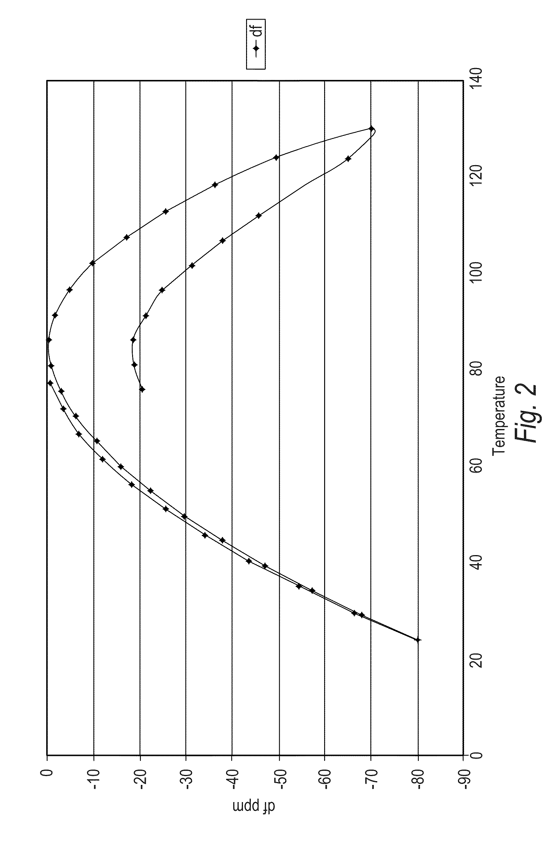
FIG. 2 is a graph illustrating changes of the center frequency of a conventional acoustic resonator structure as a function of temperature. These changes are caused by stresses on the acoustic resonator due to the changing temperature. The graph of FIG. 2 was generated with a so-called zero drift resonator (ZDR) mounted on a PCB in laboratory conditions. A resonator under real-life conditions may experience even more frequency drift than that illustrated in FIG. 2.
Referring to FIG. 2, the ZDR was heated from an initial temperature of approximately 70.degree. C. to a temperature of approximately 130.degree. C. The resonator was then cooled to approximately 25.degree. C. and heated back to approximately 70.degree. C. The center frequency of the acoustic resonator changed by approximately -50 ppm when the temperature was raised from 70.degree. C. to 130.degree. C. Then, as the temperature was cooled back to 70.degree. C., the center frequency passed through a point at 0 ppm, which is offset from the original center frequency by approximately 20 ppm. As illustrated by the different center frequencies exhibited at 70.degree. C., the center frequency of the acoustic resonator exhibits both temperature dependence as well as temperature based hysteresis. The parabolic temperature dependence is a property of the stiffness of the materials present in the acoustic stack of the ZDR and can be compensated elsewhere in the circuit. But, the hysteresis is created by variations in applied forces to the substrate. One cause for the change in force is that the epoxy (a hydrophilic material) outgases moisture and as the epoxy becomes more desiccated, it shrinks and thus applies a different force to the mounted ZDR.
The frequency changes shown in FIG. 2 may be too large for certain high accuracy electronic applications. For example, GPS devices can only tolerate aging-related frequency changes on the order of +/-0.5 ppm. Similarly, wireless applications, such as low power radios used in WiFi or Bluetooth can only tolerate aging-related frequency changes on the order of +/-10 ppm.
What is needed, therefore, are techniques for reducing frequency drift due to physical stresses in acoustic resonator structures.
BRIEF DESCRIPTION OF THE DRAWINGS
The described embodiments are best understood from the following detailed description when read with the accompanying drawing figures. It is emphasized that the various features are not necessarily drawn to scale. In fact, the dimensions may be arbitrarily increased or decreased for clarity of discussion. Wherever applicable and practical, like reference numerals refer to like elements.
FIG. 1A is a diagram illustrating forces applied to a known acoustic resonator structure.
FIG. 1B is a diagram illustrating a simulation of forces transferred from a substrate to an FBAR in the acoustic resonator structure of FIG. 1A.
FIG. 2 is a graph illustrating changes of the center frequency of a conventional acoustic resonator structure as a function of temperature.
FIG. 3 is a diagram illustrating an acoustic resonator structure according to a representative embodiment.
FIG. 4A is a diagram illustrating an acoustic resonator structure according to a representative embodiment.
FIG. 4B is a diagram illustrating an acoustic resonator structure according to a representative embodiment.
FIG. 4C is a diagram illustrating an acoustic resonator structure according to a representative embodiment.
FIG. 4D is a diagram illustrating an acoustic resonator structure according to a representative embodiment.
FIG. 5 is a diagram illustrating a simulation of forces transferred from a substrate to an acoustic resonator in the acoustic resonator structure of FIG. 4A.
FIG. 6A is a diagram illustrating stress applied to an acoustic resonator and a pedestal according to a representative embodiment.
FIG. 6B is a graph illustrating stress in the structure of FIG. 6A as a function of a z-coordinate.
FIGS. 7A through 7K are diagrams illustrating a method of fabricating an acoustic resonator structure in accordance with a representative embodiment.
FIG. 8 is a flowchart illustrating a method of fabricating an acoustic resonator structure according to a representative embodiment.
DETAILED DESCRIPTION
In the following detailed description, for purposes of explanation and not limitation, representative embodiments disclosing specific details are set forth in order to provide a thorough understanding of the present teachings. However, it will be apparent to one having ordinary skill in the art having had the benefit of the present disclosure that other embodiments according to the present teachings that depart from the specific details disclosed herein remain within the scope of the appended claims. Moreover, descriptions of well-known apparatuses and methods may be omitted so as to not obscure the description of the example embodiments. Such methods and apparatuses are clearly within the scope of the present teachings.
The terminology used herein is for purposes of describing particular embodiments only, and is not intended to be limiting. The defined terms are in addition to the technical and scientific meanings of the defined terms as commonly understood and accepted in the technical field of the present teachings. In addition, unless expressly so defined herein, terms are not to be interpreted in an overly idealized fashion. For example, the terms "isolation" or "separation" are not to be interpreted to require a complete lack of interaction between the described features.
As used in the specification and appended claims, the terms `a`, `an` and `the` include both singular and plural referents, unless the context clearly dictates otherwise. Thus, for example, `a device` includes one device and plural devices.
As used in the specification and appended claims, and in addition to their ordinary meanings, the terms `substantial` or `substantially` mean to within acceptable limits or degree.
As used in the specification and the appended claims and in addition to its ordinary meaning, the term `approximately` means to within an acceptable limit or amount to one having ordinary skill in the art. For example, `approximately the same` means that one of ordinary skill in the art would consider the items being compared to be the same. The present teachings relate generally to bulk acoustic wave (BAW) resonator structures. These resonator structures can include various types of acoustic resonators, such as, for example, FBARs, ZDRs, double bulk acoustic resonators (DBARs), and coupled resonator filters (CRFs). In certain embodiments, the BAW resonator structures can be used to provide electrical filters (e.g., ladder filters). In addition, in certain embodiments one or more acoustic resonators can be coupled to a circuit in an "FMOS" configuration, for example as described in commonly owned U.S. patent application Ser. No. 12/891,039, entitled "Packaged Device with Acoustic Resonator and Electronic Circuitry and Method of Making the Same" filed on Sep. 27, 2010, to Ruby, et al.; and Ser. No. 13/162,883 entitled "Capacitance Detector for Accelerometer and Gyroscope and Accelerometer and Gyroscope with Capacitance Detector" filed on Jun. 17, 2011 to Ruby, et al. The disclosures of these patent applications are specifically incorporated herein by reference as if set forth herein.
Certain details of BAW resonators, BAW resonator filters, related materials, and methods of fabrication may be found in one or more of the following commonly owned U.S. Patents and Patent Application Publications: U.S. Pat. No. 6,107,721, to Lakin; U.S. Pat. Nos. 5,587,620, 5,873,153, 6,060,818 and 6,507,983 to Ruby, et al.; U.S. Pat. No. 7,629,865 to Ruby, et al.: U.S. Pat. No. 7,280,007 to Feng, et al.; U.S. Patent Application Publication No. 20070205850 to Jamneala, et al.: U.S. Patent Application Publication No. 20060071736 to Ruby, et al; U.S. Patent Application Publication No. 20100327697 to Choy, et al.; and U.S. Patent Application Publication No. 20100327994 to Choy, et al. Examples of stacked bulk acoustic resonators, as well as their materials and methods of fabrication, may be found in U.S. Pat. No. 7,889,024 to Bradley et al. The disclosures of these patents and patent applications are specifically incorporated herein by reference as if set forth herein. It is emphasized that the components, materials and method of fabrication described in these patents and patent applications are representative and other methods of fabrication and materials within the purview of one of ordinary skill in the art are contemplated.
Certain embodiments described below relate to an acoustic resonator structure comprising an acoustic resonator formed on a pedestal. The pedestal supports the acoustic resonator such that forces transmitted to the pedestal produce minimal physical stress on the acoustic resonator. In other words, the pedestal mechanically isolates the acoustic resonator to prevent the acoustic resonator from being influenced by surrounding forces. In this manner, the pedestal reduces the amount of frequency drift in the acoustic resonator due to physical stress.
Certain embodiments described below can be used in electronic applications such as low power radios for wireless applications, GPS devices, and imaging devices, to name but a few. Some embodiments are particularly relevant to high accuracy devices requiring filters with minimal frequency drift. For example, some embodiments can be used to displace existing technologies such as existing Quartz based oscillators used in GPS devices. In addition, some embodiments also provide thermal isolation by forming the pedestal of a material having low thermal conductivity, which can allow the resonators to be used in thermally dynamic environments.
FIG. 3 is a diagram illustrating an acoustic resonator structure 300 according to a representative embodiment.
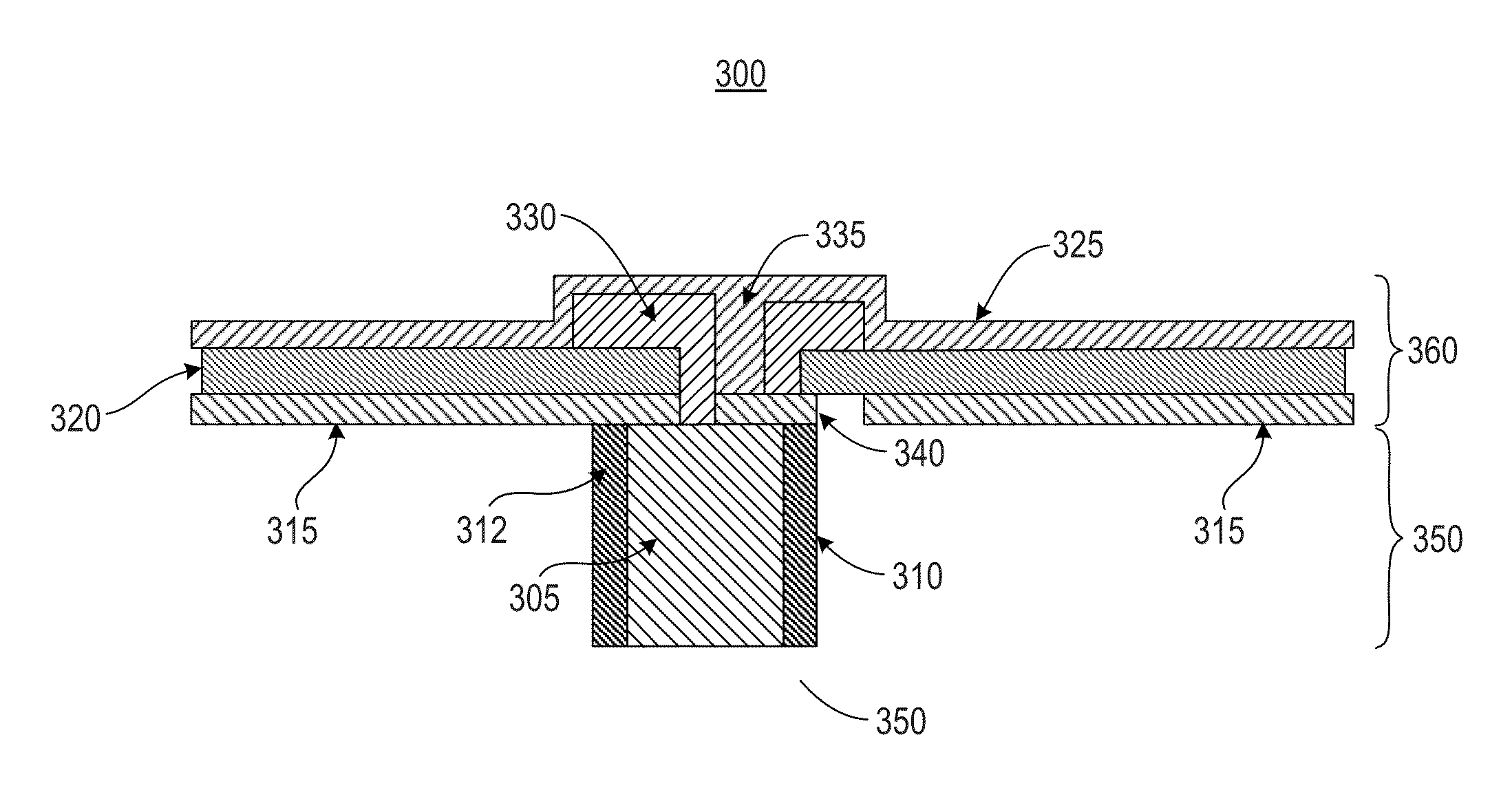
Referring to FIG. 3, acoustic resonator structure 300 comprises a pedestal 350, and an acoustic resonator 360 attached to pedestal 350 at a central location. Acoustic resonator 360 is formed in an annular shape around pedestal 350.
Pedestal 350 comprises a pillar 305, a first contact 310 and a second contact 312. First and second contacts 310 and 312 are typically formed of an electrically conductive material such as tungsten or molybdenum. First and second contacts 310, 312 are electrically isolated from each other so that first contact 310 forms a first conductive path connected to acoustic resonator 360, and second contact 312 forms a second conductive path connected to acoustic resonator 360.
Pillar 305 is illustratively silicon and typically forms part of an etched silicon wafer, as illustrated for example in FIG. 4. In some embodiments, pillar 305 can be replaced with a pillar formed of a material having lower thermal conductivity than silicon, such as a non-conductive oxide. This replacement of pillar 305 can provide improved thermal insulation for acoustic resonator 360. Illustrative examples of such a non-conductive oxide include but are not limited to silicon dioxide, which has much greater thermal resistance than pure silicon, or non-etchable boro-silica glass (NEBSG). Other materials within the purview of one of ordinary skill in the art having the benefit of the present disclosure are also contemplated for use as the materials of the pillar 305.
Acoustic resonator 360 comprises a lower electrode 315, a piezoelectric layer 320, and an upper electrode 325. At the same time that the lower electrode 315 is deposited and patterned, an `island` electrode 340 is formed covering a portion of the pedestal 350. As depicted in FIG. 3, the island electrode 340 is electrically isolated from lower electrode 315, and provides a conductive path between the upper electrode 325 and first contact 310. Lower and upper electrodes 315 and 325 and island electrode 340 are typically formed of a conductive material such as molybdenum or tungsten, or other materials described in certain referenced U.S. Patents, U.S. Patent Application Publications, and U.S. Patent Applications referenced above. Piezoelectric layer 320 can comprise, for example, aluminum nitride (AlN), zinc oxide (ZnO), or lead zirconium titanate (PZT). The piezoelectric layer 320 comprises a highly-textured c-axis piezoelectric material. Notably, in a highly textured c-axis piezoelectric material, the c-axis orientations of the crystals of the piezoelectric material are well-collimated, and as such are parallel with one another and perpendicular to the plane of the electrodes (e.g., lower and upper electrodes 315, 325).
Lower electrode 315 is electrically connected to second contact 312 on the left side of pedestal 350, and upper electrode 325 is electrically connected to first contact 310 on the right side of pedestal 350 through the island electrode 340. More specifically, lower electrode 315 is in direct contact with second contact 312, while upper electrode 325 is connected to first contact 310 through island electrode 340. Although lower electrode 315 is shown as two discontinuous sections with pedestal 350 therebetween, these sections are electrically connected and represent a single annulus.
Illustratively, the electrical connection between upper electrode 325 and first contact 310 is formed by a via 335 that connects to the island electrode 340 formed on pedestal 350 to a top portion of acoustic resonator 360. Island electrode 340 is typically formed of the same layer as lower electrode 315, but is electrically isolated from lower electrode 315. In other words, island electrode 340 can be viewed as a conductive island formed by removing a surrounding portion of lower electrode 315.
A spacer 330 is formed in a cavity between via 335 and piezoelectric layer 320. In some embodiments, spacer 330 is formed of a suitable dielectric material such as non-etchable borosilicate glass (NEBSG). In other embodiments, spacer 330 comprises an air cavity. Among other functions, spacer 330 functions to substantially prevent resonances from being generated above pedestal 350. The spacer 330 also has an annular shape and ensures that the upper electrode 325 does not form a parasitic resonance with the portion of the lower electrode 315 disposed beneath the spacer 330. Notably, the active area of the acoustic resonator 360 includes only the region where the lower and upper electrodes 315, 325 and piezoelectric layer 320 overlap and are in intimate contact with one another. As such, spacer 330 substantially prevents spurious modes from being generated between an area of lower electrode 315 directly above second contact 312, and a portion of metal connecting via 335 to the left side of upper electrode 325.
Acoustic resonator 360 has an active region defined by an overlap between lower electrode 315, the piezoelectric layer 320 and the upper electrode 325. As illustrated in FIG. 3, spacer 330 extends laterally so that no portion of upper electrode 325 is formed above pedestal 350. This allows the acoustic resonator 360 to resonate freely (i.e., substantially undamped) so that minimal energy is absorbed by pedestal 350.
During typical operation, an electrical input signal is applied between the lower electrode 315 and the upper electrode 325, causing piezoelectric layer 320 to mechanically expand and contract. As described in U.S. Patents, U.S. Patent Application Publications, and U.S. Patent Applications referenced above, longitudinal bulk acoustic waves (also referred to as longitudinal modes or thickness extensional modes) propagate through piezoelectric layer 320 and generate a corresponding electrical output signal on upper electrode 325. Notably, known structures and methods to improve the performance of the acoustic resonator 360 are contemplated by the present teachings. For example, lower and upper electrodes 315 and 325 may be apodized, and frame elements may be provided in the structure. Certain known structures and methods useful in improving the performance of the acoustic resonator are described, for example, in U.S. Patents, U.S. Patent Application Publications, and U.S. Patent Applications referenced above.
FIG. 4A is a diagram illustrating an acoustic resonator structure 400 according to a representative embodiment. In FIG. 4, a force field is shown to illustrate how a pedestal beneficially mechanically isolates the acoustic resonator structure 400 from surrounding features.
Referring to FIG. 4A, acoustic resonator structure 400 comprises a substrate 405. Substrate 405 can be formed of various types of semiconductor materials compatible with semiconductor processes, such as silicon, gallium arsenide, indium phosphide, or the like, which is useful for integrating connections and electronics, thus reducing size and cost.
A pair of trenches 420 is formed in substrate 405, and a pillar 410 (e.g., silicon or other material used for the substrate 405) is formed between trenches 420. Due to their shape, trenches 420 may be referred to alternatively as a "swimming pool" structure by those of ordinary skill in the art.
First and second electrical contacts 415 and 418 are provided within trenches 420, and an acoustic resonator 425 is formed above trenches 420 and pillar 410. Acoustic resonator 425 can be any type of bulk acoustic resonator. For example, acoustic resonator 425 can be an FBAR, DBAR, CRF, or ZDR. For explanation purposes however, acoustic resonator 425 is illustratively an FBAR. In addition, although not depicted in detail in FIG. 4A, acoustic resonator 425 comprises a lower electrode connected to a first contact on the pillar 410 that is connected to the first electrical contact 415, an upper electrode connected to a second contact on the pillar 410 that is connected to the second electrical contact 418, and a piezoelectric layer between the lower and upper electrodes. These electrodes can be connected to first and second electrical contacts 415 and 418 in a manner similar to the connection between first and second contacts 310 and 312 and lower and upper electrodes 315 and 325 in FIG. 3.
First and second electrical contacts 415 and 418, as well as the lower and upper electrodes of acoustic resonator 425, can be formed of various conductive materials, such as metals compatible with semiconductor processes, including tungsten, molybdenum, aluminum, platinum, ruthenium, niobium, or hafnium, for example. These features can also be formed with conductive sub-layers or in combination with other types of layers, such as temperature compensating layers. In addition, they can be formed of the same material, or they can be formed of different materials.
The upper electrode of acoustic resonator 425 can further comprise a passivation layer (not shown), which can be formed of various types of materials, including aluminum nitride, silicon carbide, BSG, SiO.sub.2, SiN, polysilicon, and the like. The thickness of the passivation layer should generally be sufficient to insulate the layers of acoustic resonator 425 from the environment, including protection from moisture, corrosives, contaminants, and debris.
A force field from intrinsic and/or extrinsic stimuli creates forces 430 on substrate 405. These stimuli can be caused by various factors, such as thermal expansion or contraction of a PCB connected to acoustic resonator structure 400, or attachment of a package containing acoustic resonator structure 400 to the PCB.
Forces 430 are transmitted through silicon substrate to create forces 435 on pillar 410. However, because acoustic resonator 425 is connected to pillar 410 at a single central location, forces 435 are unable to exert any appreciable torque on acoustic resonator 425. Consequently, forces 435 have minimal impact on the frequency of acoustic resonator 425. In other words, forces 435 have much less influence on the center frequency of acoustic resonator 425 compared with forces 130 of FIG. 1A.
FIG. 4B is a diagram illustrating a modified version of acoustic resonator structure 400 according to another representative embodiment. The structure shown in FIG. 4B is essentially identical to that illustrated in FIG. 4A, except that the structure of FIG. 4B further comprises tethers 440. Tethers 440 can be used to provide increased structural stability for acoustic resonator 425. Tethers 440 can be attached between first and second electrical contacts 415 and 418 and outer edges of acoustic resonator 425. Alternatively, the tethers 440 can be electrically isolated from the first and second electrical contacts 415 and 418. Moreover, tethers 440 can be connected to or formed by electrical traces (not shown) provided over the substrate 405 enabling selective electrical connections to be made to the acoustic resonator 425 suspended over the trench 420.
Although not shown in FIGS. 4A and 4B, acoustic resonator structure 400 is typically covered by a microcap structure bonded to substrate 405. The microcap structure can be formed of etched silicon or another material and enables hermetic sealing of the acoustic resonator 425. Additional details of methods, materials and assembly of a microcap structure to a base substrate may be found, for example in one or more of commonly owned U.S. Pat. Nos. 6,228,675; 6,265,246; 6,429,511; 6,787,897; 6,919,222; 6,979,597; and 7,161,283, the disclosures of which are hereby incorporated by reference as if set forth herein. In some embodiments, however, the microcap structure can be omitted.
In the embodiments depicted in and described in connection with FIGS. 4A and 4B, the pillar 410 is "centered" between trenches 420. As such, the acoustic resonator 425 is disposed symmetrically about a line 436 bisecting the pillar 410. In other embodiments contemplated by the present teachings, the pillar 410 is "offset" and the acoustic resonator 425 is not disposed symmetrically about line 436 bisecting the pillar. FIGS. 4C and 4D depict such representative embodiments. Off-setting the pillar is a form of `apodization`, where no two path lengths for lateral modes are the same. This causes a `smearing` of the lateral modes. Notably, many details of the acoustic resonator structure 400 described in connection with FIGS. 4A and 4B are common to the representative embodiments described in connection with FIGS. 4C and 4D. These common details are often not repeated in the description of the representative embodiments described in connection with FIGS. 4C and 4D.
Referring to FIG. 4C, acoustic resonator structure 400 comprises substrate 405. A first trench 441 and a second trench 442 are formed in substrate 405, and pillar 410 is formed between first and second trenches 441,442.
First and second electrical contacts 415 and 418 are provided within first and second trenches 441, 442, and acoustic resonator 425 is formed above first and second trenches 441, 442 and pillar 410. Acoustic resonator 425 can be any type of bulk acoustic resonator. For example, acoustic resonator 425 can be an FBAR, DBAR, CRF, or ZDR. For explanation purposes however, acoustic resonator 425 is illustratively an FBAR. In addition, although not depicted in detail in FIG. 4C, acoustic resonator 425 comprises a lower electrode connected to a first contact on the pillar 410 that is connected to the first electrical contact 415, an upper electrode connected to a second contact on the pillar 410 that is connected to the second electrical contact 418, and a piezoelectric layer between the lower and upper electrodes. These electrodes can be connected to first and second electrical contacts 415 and 418 in a manner similar to the connection between first and second contacts 310 and 312 and lower and upper electrodes 315 and 325 in FIG. 3.
A force field from intrinsic and/or extrinsic stimuli creates forces 430 on substrate 405. These stimuli can be caused by various factors, such as thermal expansion or contraction of a PCB connected to acoustic resonator structure 400, or attachment of a package containing acoustic resonator structure 400 to the PCB.
Forces 430 are transmitted through silicon substrate to create forces 435 on pillar 410. However, because acoustic resonator 425 is connected to pillar 410 at a single location, forces 435 are unable to exert any appreciable torque on acoustic resonator 425. Consequently, forces 435 have minimal impact on the frequency of acoustic resonator 425. In other words, forces 435 have much less influence on the center frequency of acoustic resonator 425 compared with forces 130 of FIG. 1A.
As can be appreciated from a review of FIG. 4C, acoustic resonator 425 is not symmetrically disposed over the pillar 410. As such, the pillar 410 is offset relative to a center of the acoustic resonator 425. In the present embodiment, this is achieved by offsetting the pillar 410 so that a greater portion of the acoustic resonator 425 overhangs the second trench 442 than the first trench 441. As depicted in FIG. 4C, an overhang 443 from an exterior edge of the pillar 410 to the outer edge of the acoustic resonator 425 is less than an overhang 444 from the opposing exterior edge of the pillar 410 to the outer edge of the acoustic resonator 425. Stated somewhat differently, the acoustic resonator 425 is not disposed symmetrically about line 436, which bisects the pillar 410.
As depicted in FIG. 4C, one way of offsetting of the pillar 410 is effected by forming first trench 441 to be narrower than second trench 442. However, this is not essential as width of the first trench 441 could be the same as or even greater than the width of the second trench 442, as long as the overhang of the acoustic resonator on either side of the pillar 410 is not the same (e.g., overhang 443 is less than overhang 444).
Offsetting the pillar 410 and thereby providing an unequal overhang of the acoustic resonator 425 beneficially reduce spurious modes between the inner portion of the acoustic resonator 425 and the outer portion of the acoustic resonator 425. To this end, by offsetting the center of the acoustic resonator 425 (by offsetting the pillar 410 so that the overhangs 443,444 are not equal) no single eigenmode dominates. Rather, a plurality of orthogonal eigenmodes (e.g., cylindrical Bessel functions in the annular geometry of acoustic resonator 425) is supported. Ultimately, this results in a reduction of spurious modes in the acoustic resonator 425. This is a similar phenomenon to that realized by apodizing opposing sides of the electrodes of an acoustic resonator as is known to one of ordinary skill in the art.
FIG. 4D is a diagram illustrating a modified version of acoustic resonator structure 400 according to another representative embodiment. The structure shown in FIG. 4D is essentially identical to that illustrated in FIG. 4C, except that the structure of FIG. 4D further comprises tethers 440. Tethers 440 can be used to provide increased structural stability for acoustic resonator 425. Tethers 440 can be attached between first and second electrical contacts 415 and 418 and outer edges of acoustic resonator 425. Alternatively, the tethers 440 can be electrically isolated from the first and second electrical contacts 415 and 418. Moreover, tethers 440 can be connected to or formed by electrical traces (not shown) provided over the substrate 405 enabling selective electrical connections to be made to the acoustic resonator 425 suspended over the trench 420.
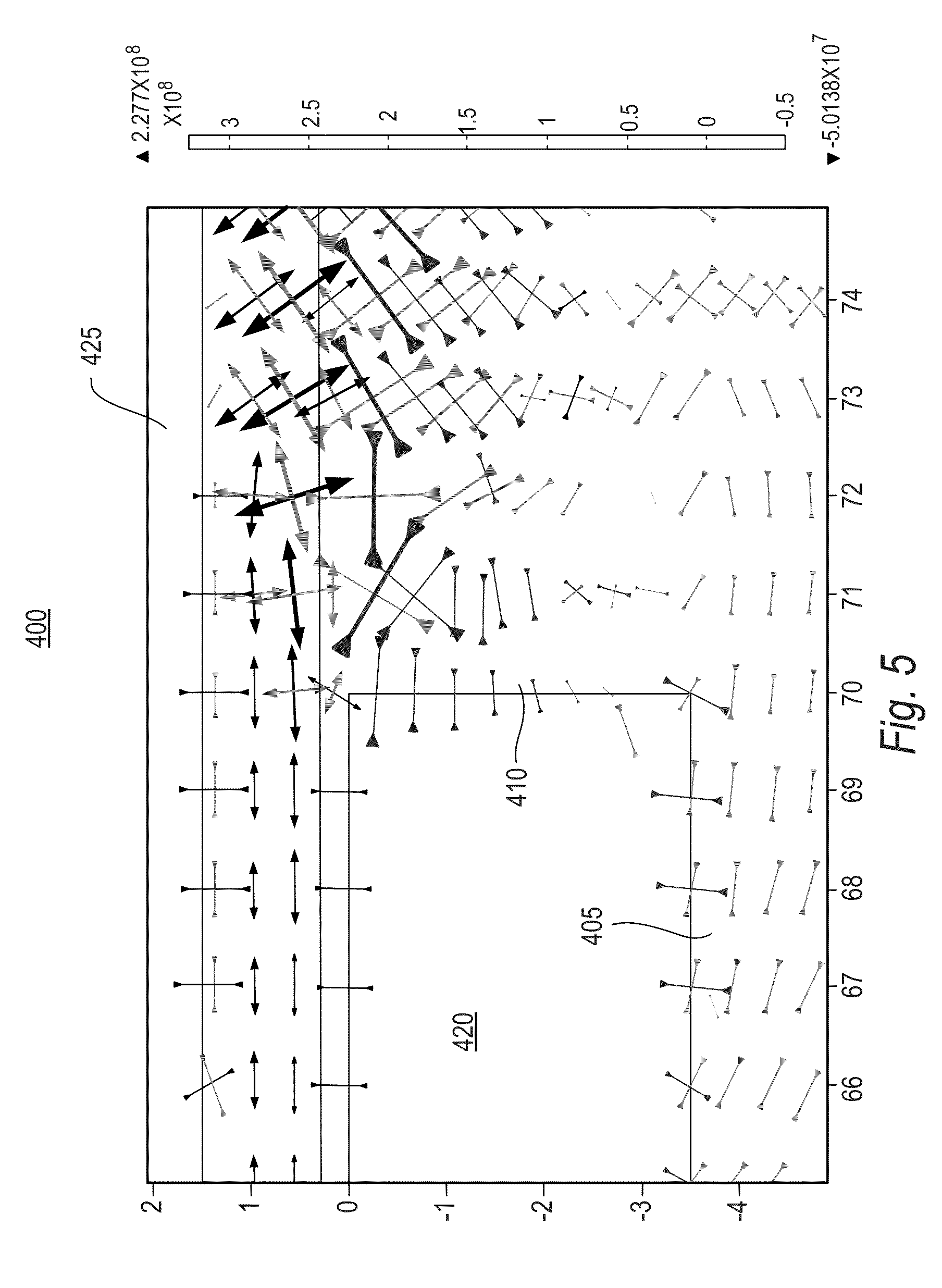
FIG. 5 is a diagram illustrating a simulation of forces transferred from substrate 405 to acoustic resonator 425 in the acoustic resonator structure of FIG. 4A.
Referring to FIG. 5, forces applied to substrate 405 are transmitted upward through pillar 410. However, because pillar 410 is located at a point of zero lever moment with respect to acoustic resonator 425, substantially none of the forces are transmitted through acoustic resonator 425.
FIG. 6A is a diagram illustrating stresses applied to an acoustic resonator and a pedestal according to a representative embodiment. The stresses are indicated generally by shading, as shown in the embedded legend. In addition, two lines 605 and 610 are included in order to highlight stresses at specific cross-sectional locations of the resonator and pedestal, as explained with reference to FIG. 6B. Notably, the diagram depicted in FIG. 6A was realized using three-dimensional finite element simulations using known software, such as finite element simulation software commercially available from Comsol, Inc. USA.
FIG. 6B is a graph illustrating stresses along lines 605 and 610 in the structure of FIG. 6A. These stresses are plotted as a function of a z-coordinate. In other words, the stresses are plotted as a function of position along lines 605 and 610.
Referring to FIG. 6B, a first curve 615 illustrates stresses on the acoustic resonator of FIG. 6A as a function of z-coordinate along line 605. A second curve 620 illustrates stresses on the pedestal of FIG. 6A as a function of z-coordinate along line 610.
As indicated by FIG. 6B, the resonator experiences horizontal stresses of approximately -20 mega pascals (MPa) to approximately +15 MPa throughout its thickness. Meanwhile, the pedestal experiences horizontal stresses of up to approximately 55 MPa. Accordingly, the stresses along line 605 in the acoustic resonator are significantly weaker than the stresses along line 610 of the pedestal. This reduction of stress in the acoustic resonator can significantly reduce the amount of aging and related frequency drift in the resonator.
FIGS. 7A through 7K are diagrams illustrating a method of fabricating an acoustic resonator structure in accordance with a representative embodiment. FIG. 7A is a top view of a substrate 705 that forms the base of the acoustic resonator structure, and FIGS. 7B through 7J are cross-sectional views showing the formation of various features of the acoustic resonator structure on substrate 705. The method can be used to fabricate an acoustic resonator structure such as that illustrated in FIGS. 3 and 4. Notably, many of the materials, processing techniques and design considerations used in the presently described method of fabricating the acoustic resonator structure are disclosed in the U.S. Patents, U.S. Patent Application Publications, and U.S. Patent Applications incorporated by reference above.
Referring to FIGS. 7A and 7B, the method begins by etching substrate 705 to form a trench 715 having a pillar 710. Illustratively, substrate 705 and pillar 710 comprise silicon or other suitable (e.g., semiconductor) material. Trench 715 forms an annulus around pillar 710 so that an acoustic resonator having an annular shape can be formed above trench 715 and over the pillar 710. Although trench 715 depicted has a substantially circular shape, this is merely illustrative, and the trench 715 it can also take other forms, such as by way of example, an elliptical shape, a square shape, a rectangular shape or an irregular shape. Illustratively, pillar 710 has a rectangular cross-sectional shape with a size (1.times.w) on the order of 16 .mu.m.times.32 .mu.m. As can be appreciated the pillar 710 has a height that is approximately equal to the depth of the trench 715
Referring to FIG. 7C, an electrically conductive layer 720 is formed in trench 715 and on substrate 705. Electrically conductive layer 720 is typically divided into two portions to provide separate conductive paths to respective lower and upper electrodes of an acoustic resonator. This can be accomplished, for example, by etching electrically conductive layer 720. In some embodiments, electrically conductive layer 720 comprises tungsten or molybdenum with a thickness of approximately 1 .mu.m to approximately 2 .mu.m. Electrically conductive layer 720 provides electrical connections (e.g., first and second electrical contacts 415, 418) between an acoustic resonator disposed on the pillar 710 (e.g., acoustic resonator 425) and circuitry (e.g., an integrated circuit not shown) on the substrate 705. In some embodiments, as illustrated in FIG. 7D, an etch stop layer 725 for chemical mechanical polishing (CMP) is formed in trench 715 and on substrate 705 before electrically conductive layer 720 is formed. Etch stop layer 725 can be formed of a suitable etch stop material such as AlN or silicon carbide.
Referring to FIG. 7E, CMP is performed to remove electrically conductive layer 720 to the upper surface of substrate 705, but not from the trench 715 or sides of the pillar 710. Then, a sacrificial layer 730 of is provided in the trench 715 and over substrate 705, and CMP is again performed to remove portions of sacrificial layer 730 above substrate 705. As such, the sacrificial layer is substantially flush with the upper surface of the substrate. The sacrificial layer 730 is illustratively phosphosilicate glass (PSG) or other material such as described in one or more of the U.S. Patents, U.S. Patent Application Publications and U.S. Patent Applications incorporated by reference above.
Referring to FIG. 7F, a seed layer (not shown) is deposited on sacrificial layer 730. Next, an electrically conductive layer 735 (e.g., molybdenum) is deposited on the seed layer. Electrically conductive layer 735 is used to form a lower electrode for the acoustic resonator. The seed layer provides a barrier to oxygen migration from the sacrificial layer 730 (e.g., PSG) through the lower electrode (formed from electrically conductive layer 735) and contaminating the piezoelectric layer during its deposition. Then, optionally, a temperature compensation layer (not shown) is formed on electrically conductive layer 735. The temperature compensation layer typically comprises borosilicate glass (BSG) or undoped silicate glass (USG). For simplicity of description, because the temperature compensation layer is located away from the pillar 710 and the outer edge of the acoustic resonator, it is not depicted.
Referring to FIG. 7G, electrically conductive layer 735 is patterned at specific locations to define the lower electrode of the acoustic resonator, and to create a conductive path for connecting electrically conductive layer 720 to a upper electrode of the acoustic resonator (e.g., as depicted in FIG. 3). Although not shown in FIG. 7G, a temperature compensation layer typically remains on the structure shown.
Referring to FIG. 7H, a piezoelectric layer 750 is deposited over electrically conductive layer 735. Piezoelectric layer 750 typically comprises a highly-textured c-axis piezoelectric material such as AIN or ZnO and provides the piezoelectric layer of the acoustic resonator of the representative embodiment.
Referring to FIG. 7I, a layer of PSG or NEBSG is deposited on piezoelectric layer 750. The layer of PSG or NEBSG is then patterned to form spacer elements 755. In addition, a via (not shown) is formed to expose a portion of electrically conductive layer 735. The exposed portion of electrically conductive layer 735 can take the form of an island similar to island electrode 340 depicted in FIG. 3. The via can be used to form an electrical connection between the electrically conductive layer 720 and an upper electrode of the acoustic resonator.
Referring to FIG. 7J, an electrically conductive layer (e.g., Mo) 760 is formed on piezoelectric layer 750 and over spacer elements 755. Electrically conductive layer 760 is used to form the upper electrode for the acoustic resonator. In addition, electrically conductive layer 760 fills the via to connect the upper electrode to electrically conductive layer 720. A passivation layer (not shown) is formed on the electrically conductive layer 760, and the passivation layer is patterned to form a passivation mask. Then, electrically conductive layer 760 is patterned using the passivation mask. This patterning defines the upper electrode of the acoustic resonator. Once the upper electrode is formed, the acoustic resonator has an active region defined by an overlap between the upper electrode, the lower electrode, and piezoelectric layer 750. Electrical contact pads 765 are then formed on electrically conductive layer 760. These electrical contact pads 765 are typically formed of a conductive material such as gold.
As depicted in FIG. 7K, sacrificial layer 730 is removed using a known method so that the acoustic resonator is suspended over the trench 715 and supported by pillar 710. This provides mechanical isolation for the acoustic resonator as described above, for example in connection with FIGS. 3 and 4, in order to substantially prevent the acoustic resonator from experiencing frequency drift due to stresses from external forces.
FIG. 8 is a flowchart illustrating a method of fabricating an acoustic resonator structure according to a representative embodiment. The method of FIG. 8 is similar to the method described with reference to FIGS. 7A through 7J, and it will be described with occasional reference to those figures. In the description of FIG. 8, example method steps are indicated by parentheses (SXXX) to distinguish them from example apparatus features.
Referring to FIG. 8, the method begins by forming a trench having a pillar in a silicon substrate (S805). Next, the method forms a conductive pattern in the trench (S810). The conductive pattern comprises a first part used to provide an electrical connection to a lower electrode of the acoustic resonator structure, and a second part used to provide an electrical connection to an upper electrode of the acoustic resonator structure. The conductive pattern can be formed, for example, by depositing a layer of tungsten in the trench and the removing portions of the tungsten layer from upper surfaces of the silicon substrate.
Next, a sacrificial layer (e.g., PSG) layer is formed in the trench (S815), and the sacrificial layer is planarized to the top surface of the silicon substrate. The sacrificial layer is typically removed subsequently to form an air gap in the acoustic resonator structure. In addition, the sacrificial layer serves to support other features during fabrication.
A lower electrode is formed on the silicon substrate and in contact with the conductive pattern (S820). The contact between the lower electrode and the conductive pattern can be made, for example, like the contact in FIG. 3 between lower electrode 315 and second contact 312.
Next, a piezoelectric layer is formed over the lower electrode (S825), and the piezoelectric layer is patterned to create a via extending to the second part of the conductive pattern. Then, an upper electrode is formed over the piezoelectric layer (S830). The upper electrode is electrically connected to the second part of the conductive pattern through the via, and the PSG layer is removed so that the acoustic resonator comprising the lower electrode, the piezoelectric layer, and the upper electrode is suspended over an air gap located in the trench.
While example embodiments are disclosed herein, one of ordinary skill in the art will appreciate that many variations that are in accordance with the present teachings are possible and remain within the scope of the appended claims. The invention therefore is not to be restricted except within the scope of the appended claims.
* * * * *
References
D00000
D00001
D00002
D00003
D00004
D00005
D00006
D00007
D00008
D00009
D00010
D00011
D00012

D00013

D00014

D00015
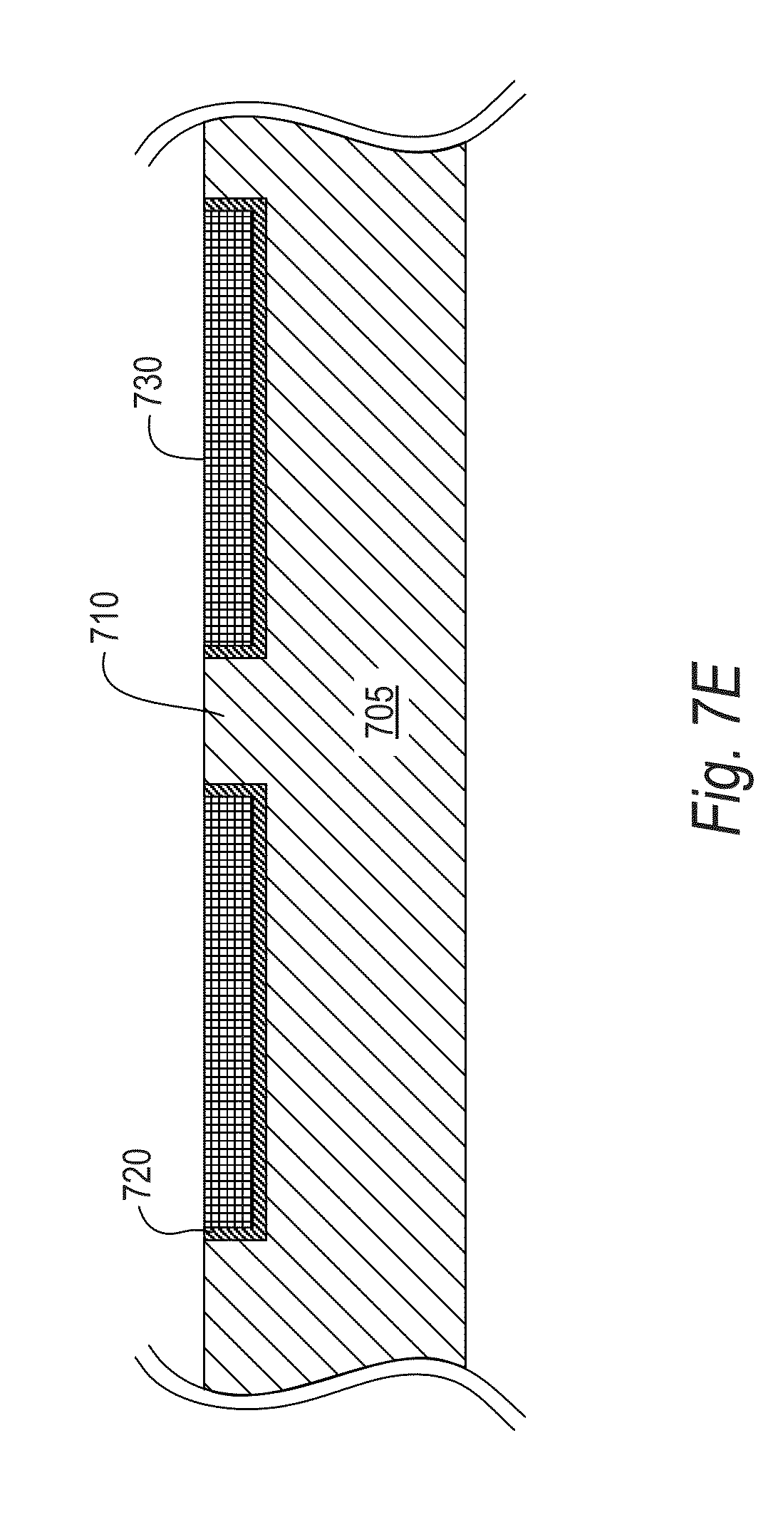
D00016

D00017

D00018

D00019

D00020

D00021
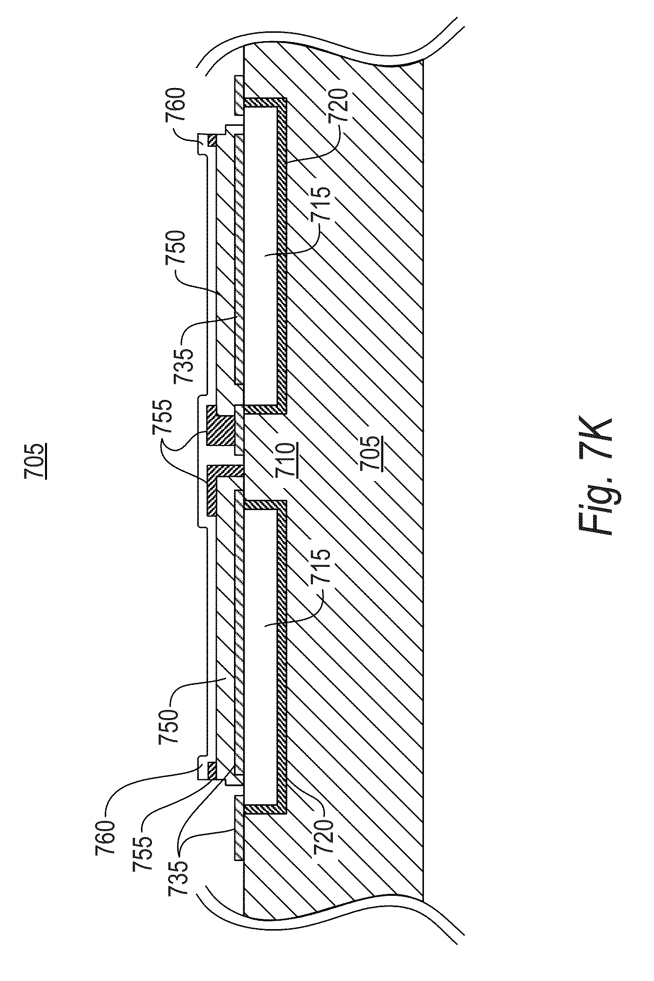
D00022

XML
uspto.report is an independent third-party trademark research tool that is not affiliated, endorsed, or sponsored by the United States Patent and Trademark Office (USPTO) or any other governmental organization. The information provided by uspto.report is based on publicly available data at the time of writing and is intended for informational purposes only.
While we strive to provide accurate and up-to-date information, we do not guarantee the accuracy, completeness, reliability, or suitability of the information displayed on this site. The use of this site is at your own risk. Any reliance you place on such information is therefore strictly at your own risk.
All official trademark data, including owner information, should be verified by visiting the official USPTO website at www.uspto.gov. This site is not intended to replace professional legal advice and should not be used as a substitute for consulting with a legal professional who is knowledgeable about trademark law.