Display panel and display device
Zhu April 5, 2
U.S. patent number 11,294,248 [Application Number 16/769,330] was granted by the patent office on 2022-04-05 for display panel and display device. This patent grant is currently assigned to SHENZHEN CHINA STAR OPTOELECTRONICS SEMICONDUCTOR DISPLAY TECHNOLOGY CO., LTD.. The grantee listed for this patent is SHENZHEN CHINA STAR OPTOELECTRONICS SEMICONDUCTOR DISPLAY TECHNOLOGY CO., LTD.. Invention is credited to Jing Zhu.


| United States Patent | 11,294,248 |
| Zhu | April 5, 2022 |
Display panel and display device
Abstract
A display panel and a display device are provided. The display panel includes a capacitive electrode layer and pixel electrode layer which form a storage capacitor. An orthographic projection of first capacitor units of the capacitive electrode layer on the pixel electrode layer is located within a first trunk electrode or/and a second trunk electrode. Due to the orthographic projection of the capacitive electrode layer on the pixel electrode layer is located within a trunk electrode, a display aperture ratio is increased.
| Inventors: | Zhu; Jing (Guangdong, CN) | ||||||||||
|---|---|---|---|---|---|---|---|---|---|---|---|
| Applicant: |
|
||||||||||
| Assignee: | SHENZHEN CHINA STAR OPTOELECTRONICS
SEMICONDUCTOR DISPLAY TECHNOLOGY CO., LTD. (Shenzhen,
CN) |
||||||||||
| Family ID: | 1000006218962 | ||||||||||
| Appl. No.: | 16/769,330 | ||||||||||
| Filed: | April 14, 2020 | ||||||||||
| PCT Filed: | April 14, 2020 | ||||||||||
| PCT No.: | PCT/CN2020/084690 | ||||||||||
| 371(c)(1),(2),(4) Date: | June 03, 2020 | ||||||||||
| PCT Pub. No.: | WO2021/196276 | ||||||||||
| PCT Pub. Date: | October 07, 2021 |
Prior Publication Data
| Document Identifier | Publication Date | |
|---|---|---|
| US 20210302794 A1 | Sep 30, 2021 | |
Foreign Application Priority Data
| Mar 31, 2020 [CN] | 202010241619.7 | |||
| Current U.S. Class: | 1/1 |
| Current CPC Class: | G02F 1/134309 (20130101); G02F 1/136213 (20130101); G02F 2201/40 (20130101); G02F 1/1368 (20130101); G02F 2201/123 (20130101); G02F 1/136209 (20130101) |
| Current International Class: | G02F 1/1362 (20060101); G02F 1/1343 (20060101); G02F 1/1368 (20060101) |
References Cited [Referenced By]
U.S. Patent Documents
| 9841641 | December 2017 | Hirosawa |
| 2013/0293799 | November 2013 | Lee et al. |
| 2016/0131951 | May 2016 | Lee et al. |
| 2016/0195788 | July 2016 | Bae |
| 2018/0329241 | November 2018 | Wang |
| 2020/0050065 | February 2020 | Zang et al. |
| 2020/0241340 | July 2020 | Chen |
| 103389599 | Nov 2013 | CN | |||
| 105572996 | May 2016 | CN | |||
| 105589270 | May 2016 | CN | |||
| 107238990 | Oct 2017 | CN | |||
| 107316873 | Nov 2017 | CN | |||
| 110491886 | Nov 2019 | CN | |||
Attorney, Agent or Firm: The Roy Gross Law Firm, LLC Gross; Roy
Claims
What is claimed is:
1. A display panel, comprising a first substrate, a driving circuit layer disposed on the first substrate, and a pixel electrode layer disposed on the driving circuit layer, wherein the pixel electrode layer comprises at least one first trunk electrode and at least one second trunk electrode; wherein the display panel further comprises a capacitive electrode layer arranged in the same layer as the driving circuit layer, and the capacitive electrode layer and a portion of the pixel electrode layer together form a storage capacitor; wherein the capacitive electrode layer at least comprises a plurality of first capacitor units, an orthographic projection of one of the first capacitor units on the pixel electrode layer is located within the first trunk electrode or/and the second trunk electrode, and the first trunk electrode is arranged vertically to the second trunk electrode; wherein the capacitive electrode layer further comprises a plurality of second capacitor units; the first capacitor units and the second capacitor units are connected in parallel; the first capacitor units and a source/drain layer of the driving circuit layer are arranged in the same layer; the orthographic projection of one of the first capacitor units on the pixel electrode layer is located within the first trunk electrode; the second capacitor units and any one of a light-shielding layer of the driving circuit layer or a semiconductor layer of the driving circuit layer are arranged in the same layer; and another orthographic projection of one of the second capacitor units on the pixel electrode layer is located within the first trunk electrode.
2. The display panel as claimed in claim 1, wherein the first capacitor units and a gate layer of the driving circuit layer are arranged in the same layer; and the orthographic projection of one of the first capacitor units on the pixel electrode layer is located within the second trunk electrode.
3. The display panel as claimed in claim 1, wherein the first capacitor units and a light-shielding layer of the driving circuit layer are arranged in the same layer.
4. The display panel as claimed in claim 1, wherein the first capacitor units and a semiconductor layer of the driving circuit layer are arranged in the same layer.
5. The display panel as claimed in claim 1, wherein the capacitive electrode layer further comprises a plurality of third capacitor units; the third capacitor units are formed in a pixel light-transmitting area of the display panel; and the third capacitor units are made of a transparent material.
6. The display panel as claimed in claim 5, wherein the third capacitor units and the first capacitor units are connected in parallel.
7. The display panel as claimed in claim 6, wherein the third capacitor units and the source/drain layer of the driving circuit layer are arranged in the same layer; and the first capacitor units are parallel to the third capacitor units.
8. A display device, comprising a display panel, a polarizer layer, and a cover plate layer, wherein the polarizer layer and the cover plate layer are disposed on the display panel; wherein the display panel comprises a first substrate, a driving circuit layer disposed on the first substrate, and a pixel electrode layer disposed on the driving circuit layer, wherein the pixel electrode layer comprises at least one first trunk electrode and at least one second trunk electrode; wherein the display panel further comprises a capacitive electrode layer arranged in the same layer as the driving circuit layer, and the capacitive electrode layer and a portion of the pixel electrode layer together form a storage capacitor; wherein the capacitive electrode layer at least comprises a plurality of first capacitor units, an orthographic projection of one of the first capacitor units on the pixel electrode layer is located within the first trunk electrode or/and the second trunk electrode, and the first trunk electrode is arranged vertically to the second trunk electrode; wherein the capacitive electrode layer further comprises a plurality of second capacitor units; the first capacitor units and the second capacitor units are connected in parallel; the first capacitor units and a source/drain layer of the driving circuit layer are arranged in the same layer; the orthographic projection of one of the first capacitor units on the pixel electrode layer is located within the first trunk electrode; the second capacitor units and any one of a light-shielding layer of the driving circuit layer or a semiconductor layer of the driving circuit layer are arranged in the same layer; and another orthographic projection of one of the second capacitor units on the pixel electrode layer is located within the first trunk electrode.
9. The display device as claimed in claim 8, wherein the first capacitor units and a gate layer of the driving circuit layer are arranged in the same layer; and the orthographic projection of one of the first capacitor units on the pixel electrode layer is located within the second trunk electrode.
10. The display device as claimed in claim 8, wherein the first capacitor units and a light-shielding layer of the driving circuit layer are arranged in the same layer.
11. The display device as claimed in claim 8, wherein the first capacitor units and a semiconductor layer of the driving circuit layer are arranged in the same layer.
12. The display device as claimed in claim 8, wherein the capacitive electrode layer further comprises a plurality of third capacitor units; the third capacitor units are formed in a pixel light-transmitting area of the display panel; and the third capacitor units are made of a transparent material.
13. The display device as claimed in claim 12, wherein the third capacitor units and the first capacitor units are connected in parallel.
14. The display device as claimed in claim 13, wherein the third capacitor units and the source/drain layer of the driving circuit layer are arranged in the same layer; and the first capacitor units are parallel to the third capacitor units.
Description
FIELD OF DISCLOSURE
The present disclosure relates to the field of displays, in particular to the field of display technologies, and in particular to a display panel and a display device.
BACKGROUND
With an improvement of living standards, people's demand for large-size and high-resolution display screens is increasing.
In the prior art, a storage capacitor of a large-size and high-resolution display screen is composed of a common electrode and a pixel electrode, where the opaque common electrode causes a display aperture ratio of the display screen to be low.
Therefore, a display panel and a display device are necessary to solve the above technical problems.
SUMMARY OF DISCLOSURE
In the prior art, a storage capacitor of a large-size and high-resolution display screen is composed of a common electrode and a pixel electrode, where the opaque common electrode causes a display aperture ratio of the display screen to be low. The present disclosure provides a display panel and a display device to solve the above technical problems.
To solve the above problems, technical solutions provided by the present disclosure are as follows.
A display panel includes a first substrate, a driving circuit layer disposed on the first substrate, and a pixel electrode layer disposed on the driving circuit layer, where the pixel electrode layer includes at least one first trunk electrode and at least one second trunk electrode.
The display panel further includes a capacitive electrode layer arranged in the same layer as the driving circuit layer, and the capacitive electrode layer and a portion of the pixel electrode layer together form a storage capacitor.
The capacitive electrode layer at least includes a plurality of first capacitor units, an orthographic projection of one of the first capacitor units on the pixel electrode layer is located within the first trunk electrode or/and the second trunk electrode, and the first trunk electrode is arranged vertically to the second trunk electrode.
In the display panel of the present disclosure, the first capacitor units and a source/drain layer of the driving circuit layer are arranged in the same layer.
The orthographic projection of one of the first capacitor units on the pixel electrode layer is located within the first trunk electrode.
In the display panel of the present disclosure, the first capacitor units and a gate layer of the driving circuit layer are arranged in the same layer.
The orthographic projection of one of the first capacitor units on the pixel electrode layer is located within the second trunk electrode.
In the display panel of the present disclosure, the first capacitor units and a light-shielding layer of the driving circuit layer are arranged in the same layer.
In the display panel of the present disclosure, the first capacitor units and a semiconductor layer of the driving circuit layer are arranged in the same layer.
In the display panel of the present disclosure, the capacitive electrode layer further includes a plurality of second capacitor units.
The first capacitor units and the second capacitor units are connected in parallel.
The first capacitor units and a source/drain layer of the driving circuit layer are arranged in the same layer.
The orthographic projection of one of the first capacitor units on the pixel electrode layer is located within the first trunk electrode.
The second capacitor units and any one of a light-shielding layer of the driving circuit layer or a semiconductor layer of the driving circuit layer are arranged in the same layer.
Another orthographic projection of one of the second capacitor units on the pixel electrode layer is located within the first trunk electrode.
In the display panel of the present disclosure, the capacitive electrode layer further includes a plurality of third capacitor units.
The third capacitor units are formed in a pixel light-transmitting area of the display panel.
The third capacitor units are made of a transparent material.
In the display panel of the present disclosure, the third capacitor units and the first capacitor units are connected in parallel.
The first capacitor units and a source/drain layer of the driving circuit layer are arranged in the same layer.
The orthographic projection of one of the first capacitor units on the pixel electrode layer is located with the first trunk electrode.
In the display panel of the present disclosure, the third capacitor units and the source/drain layer of the driving circuit layer are arranged in the same layer.
The first capacitor units are parallel to the third capacitor units.
In the display panel of the present disclosure, the capacitive electrode layer further includes a plurality of second capacitor units.
The second capacitor units and the first capacitor units are connected in parallel.
The second capacitor units and any one of a light-shielding layer of the driving circuit layer or a semiconductor layer of the driving circuit layer are arranged in the same layer.
Another orthographic projection of one of the second capacitor units on the pixel electrode layer is located within the first trunk electrode.
A display device includes a display panel, a polarizer layer, and a cover plate layer, where the polarizer layer and the cover plate layer are disposed on the display panel;
The display panel includes a first substrate, a driving circuit layer disposed on the first substrate, and a pixel electrode layer disposed on the driving circuit layer, where the pixel electrode layer includes at least one first trunk electrode and at least one second trunk electrode.
The display panel further includes a capacitive electrode layer arranged in the same layer as the driving circuit layer, and the capacitive electrode layer and a portion of the pixel electrode layer together form a storage capacitor.
The capacitive electrode layer at least includes a plurality of first capacitor units, an orthographic projection of one of the first capacitor units on the pixel electrode layer is located within the first trunk electrode or/and the second trunk electrode, and the first trunk electrode is arranged vertically to the second trunk electrode.
In the display device of the present disclosure, the first capacitor units and a source/drain layer of the driving circuit layer are arranged in the same layer.
The orthographic projection of one of the first capacitor units on the pixel electrode layer is located within the first trunk electrode.
In the display device of the present disclosure, the first capacitor units and a gate layer of the driving circuit layer are arranged in the same layer.
The orthographic projection of one of the first capacitor units on the pixel electrode layer is located within the second trunk electrode.
In the display device of the present disclosure, the first capacitor units and a light-shielding layer of the driving circuit layer are arranged in the same layer.
In the display device of the present disclosure, the first capacitor units and a semiconductor layer of the driving circuit layer are arranged in the same layer.
In the display device of the present disclosure, the capacitive electrode layer further includes a plurality of second capacitor units.
The first capacitor units and the second capacitor units are connected in parallel.
The first capacitor units and a source/drain layer of the driving circuit layer are arranged in the same layer.
The orthographic projection of one of the first capacitor units on the pixel electrode layer is located within the first trunk electrode.
The second capacitor units and any one of a light-shielding layer of the driving circuit layer or a semiconductor layer of the driving circuit layer are arranged in the same layer.
Another orthographic projection of one of the second capacitor units on the pixel electrode layer is located within the first trunk electrode.
In the display device of the present disclosure, the capacitive electrode layer further includes a plurality of third capacitor units.
The third capacitor units are formed in a pixel light-transmitting area of the display panel.
The third capacitor units are made of a transparent material.
In the display device of the present disclosure, the third capacitor units and the first capacitor units are connected in parallel.
The first capacitor units and a source/drain layer of the driving circuit layer are arranged in the same layer.
The orthographic projection of one of the first capacitor units on the pixel electrode layer is located with the first trunk electrode.
In the display device of the present disclosure, the third capacitor units and the source/drain layer of the driving circuit layer are arranged in the same layer.
The first capacitor units are parallel to the third capacitor units.
In the display device of the present disclosure, the capacitive electrode layer further includes a plurality of second capacitor units.
The second capacitor units and the first capacitor units are connected in parallel.
The second capacitor units and any one of a light-shielding layer of the driving circuit layer or a semiconductor layer of the driving circuit layer are arranged in the same layer.
Another orthographic projection of one of the second capacitor units on the pixel electrode layer is located within the first trunk electrode.
In the present disclosure, due to the orthographic projection of the capacitive electrode layer on the pixel electrode layer is located within a trunk electrode, a display aperture ratio is increased.
BRIEF DESCRIPTION OF DRAWINGS
FIG. 1 is a top view of a first structure of a display panel of the present disclosure.
FIG. 2 is a schematic diagram of the first structure of the display panel of the present disclosure.
FIG. 3 is a schematic diagram of a second structure of a display panel of the present disclosure.
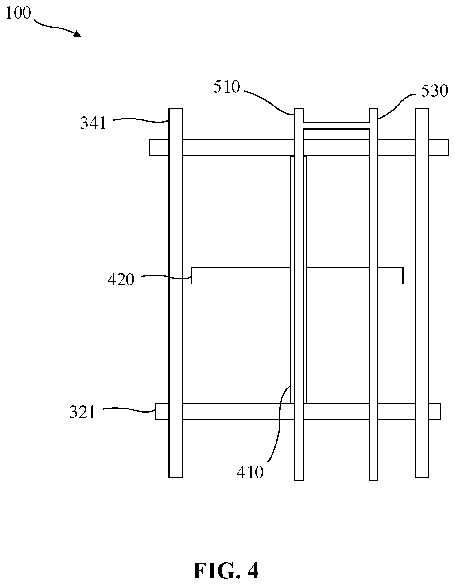
FIG. 4 is a top view of a third structure of a display panel of the present disclosure.
FIG. 5 is a schematic diagram of a display device of the present disclosure.
DETAILED DESCRIPTION
The present disclosure provides a display panel and a display device. In order to more clearly describe the technical solutions of the embodiments of the present disclosure, accompanying drawings to be used in the detailed description of the disclosure will be briefly described hereinbelow. It should be understood that the specific embodiments described herein are only used to explain the present disclosure, and are not used to limit the present disclosure.
Please refer to FIG. 1 to FIG. 4, the present disclosure discloses a display panel 100. The display panel 100 includes a first substrate 200, a driving circuit layer 300 disposed on the first substrate 200, and a pixel electrode layer 400 disposed on the driving circuit layer 300. The pixel electrode layer 400 includes at least one first trunk electrode 410 and at least one second trunk electrode 420.
The display panel 100 further includes a capacitive electrode layer arranged in the same layer as the driving circuit layer 300. The capacitive electrode layer and a portion of the pixel electrode layer 400 together form a storage capacitor.
The capacitive electrode layer at least includes a plurality of first capacitor units 510. An orthographic projection of one of the first capacitor units 510 on the pixel electrode layer 400 is located within the first trunk electrode 410 or/and the second trunk electrode 420. The first trunk electrode 410 and the second trunk electrode 420 are arranged vertically.
In the present disclosure, due to the orthographic projection of the capacitive electrode layer on the pixel electrode layer is located within a trunk electrode, a display aperture ratio is increased.
The technical solutions of the present disclosure will now be described with reference to specific embodiments.
Please refer to FIG. 1 to FIG. 4, the display panel 100 includes the first substrate 200, a driving circuit layer 300 disposed on the first substrate 200, and the pixel electrode layer 400 disposed on the driving circuit layer 300. The pixel electrode layer 400 includes at least one first trunk electrode 410 and at least one second trunk electrode 420. The display panel 100 further includes the capacitive electrode layer arranged in the same layer as the driving circuit layer 300. The capacitive electrode layer and a portion of the pixel electrode layer 400 together form the storage capacitor.
For ease of understanding, the following embodiments use a color filter on array (COA) substrate as an example for description, and do not limit the display panel 100.
In this embodiment, the driving circuit layer 300 includes a gate layer 320, a gate insulating layer 330 disposed on the gate layer 320, and a source/drain layer 340 disposed on the gate insulating layer 330. For details, please refer to FIG. 2 and FIG. 3.
In this embodiment, the gate layer 320 includes a plurality of gate lines 321 arranged in parallel. The gate line 321 is arranged along a second direction. The second direction is parallel to the second trunk electrode, please refer to FIG. 1 and FIG. 4 for details.
In this embodiment, the source/drain layer 340 includes a plurality of data lines 341 arranged in parallel. The data line 341 and the gate line 321 are vertically arranged. The data line 341 is arranged along a first direction. The first direction is parallel to the first trunk electrode, please refer to FIG. 1 and FIG. 4 for details.
In this embodiment, the driving circuit layer 300 further includes a semiconductor layer. The semiconductor layer is an active layer. The semiconductor layer may be disposed on the source/drain layer 340. Alternatively, the semiconductor layer may be disposed on the gate insulating layer 330. Alternatively, the gate layer 320 is disposed on the semiconductor layer, and the semiconductor layer is disposed on the first substrate 200. The specific position of the semiconductor layer is not limited here.
In this embodiment, the display panel 100 further includes a color film layer and a liquid crystal layer disposed on the pixel electrode layer 400.
In this embodiment, the pixel electrode layer 400 includes a plurality of pixel electrodes, and the capacitive electrode layer may form a storage capacitor with the corresponding pixel electrode.
In this embodiment, the capacitive electrode layer at least includes a plurality of first capacitor units 510. An orthographic projection of one of the first capacitor units 510 on the pixel electrode layer 400 is located within the first trunk electrode 410 or/and the second trunk electrode 420. The first trunk electrode 410 and the second trunk electrode 420 are vertically arranged, please refer to FIG. 1 for details. The first trunk electrode 410 and the second trunk electrode 420 do not emit light, forming a shielding area. By setting the first capacitor units 510 under the trunk electrode, the first capacitor units 510 are shielded by dark lines of the trunk electrode, thereby reducing a border of the display screen, increasing a display aperture ratio of the display panel 100, and improving a display performance.
In this embodiment, the first capacitor units 510 and the source/drain layer 340 of the driving circuit layer 300 are arranged in the same layer. The orthographic projection of one of the first capacitor units 510 on the pixel electrode layer 400 is located within the first trunk electrode 410, please refer to FIG. 2 for details. The source/drain layer 340 includes a plurality data lines 341. The data lines 341 are arranged along the first direction. In order to avoid contact between the first capacitor units 510 and the data lines 341 and cause a short circuit, when the first capacitor units 510 and the source/drain layer 340 of the driving circuit layer 300 are arranged in the same layer, the orthographic projection of one of the first capacitor units 510 on the electrode layer 400 is located within the first trunk electrode 410. A wiring space of the source/drain layer 340 can be better used, to avoid contact between the first capacitor units 510 and the data lines 341 to cause the short circuit, and also setting methods, such as jumper wires, is avoided, which simplifies the manufacturing process. When the first capacitor units 510 and the source/drain layer 340 of the driving circuit layer 300 are arranged in the same layer, the capacitive electrode layer and a portion of the pixel electrode layer 400 together form the storage capacitor. A spacing between the capacitive electrode layer and the portion of the pixel electrode layer 400 is small, that is, the spacing between two electrode plates of the storage capacitor is small. The storage capacitor can be provided with a larger capacitance, and a voltage difference between the two electrode plates is greater, the storage capacitor is charged faster, the charging efficiency is higher, and the display performance is better.
In this embodiment, the first capacitor units 510 and the gate layer 320 of the driving circuit layer 300 are arranged in the same layer. The orthographic projection of one of the first capacitor units 510 on the pixel electrode layer 400 is located within the second trunk electrode 420. The gate layer 320 includes a plurality of gate lines 321, and the gate lines 321 are arranged along the second direction. In order to avoid contact between the first capacitor units 510 and the gate lines 321 and cause a short circuit, when the first capacitor units 510 and the gate layer 320 of the driving circuit layer 300 are arranged in the same layer, the orthographic projection of one of the first capacitor units 510 on the pixel electrode layer 400 is located within the second trunk electrode 420. A wiring space of the gate layer 320 can be better used, to avoid contact between the first capacitor units 510 and the gate lines 321 to cause the short circuit, and also setting methods, such as jumper wires, is avoided, which simplifies the manufacturing process.
In this embodiment, the first capacitor units 510 and the light-shielding layer 310 of the driving circuit layer 300 are arranged in the same layer. When the first capacitor units 510 and the light-shielding layer 310 of the driving circuit layer 300 are arranged in the same layer, the orthographic projection of one of the first capacitor units 510 on the pixel electrode layer 400 is located within the first trunk electrode 410 or/and the second trunk electrode 420. The first capacitor may be shielded by the trunk electrode according to a specific pattern of the light-shielding layer 310. Using the dark lines of the trunk electrode to shield the first capacitor units 510, a border of the display screen is reduced, the display aperture ratio of the display panel 100 is increased, and the display performance is improved.
In this embodiment, the first capacitor units 510 and the semiconductor layer of the driving circuit layer 300 are arranged in the same layer. When the first capacitor units 510 and the semiconductor layer of the driving circuit layer 300 are arranged in the same layer, the orthographic projection of one of the first capacitor units 510 on the pixel electrode layer 400 is located within the first trunk electrode 410 or/and the second trunk electrode 420. The first capacitor may be shielded by the trunk electrode according to a specific pattern of the semiconductor layer. Using the dark lines of the trunk electrode to shield the first capacitor units 510, a border of the display screen is reduced, the display aperture ratio of the display panel 100 is increased, and the display performance is improved.
In this embodiment, the capacitive electrode layer further includes a plurality of second capacitor units 520. The first capacitor units 510 and the second capacitor units 520 are connected in parallel. The first capacitor units 510 and the source/drain layer 340 of the driving circuit layer 300 are arranged in the same layer. The orthographic projection of one of the first capacitor units 510 on the pixel electrode layer 400 is located within the first trunk electrode 410. The second capacitor units 520 and any one of the light-shielding layer 310 of the driving circuit layer 300 or the semiconductor layer of the driving circuit layer 300 are arranged in the same layer. An orthographic projection of one of the second capacitor units 520 on the pixel electrode layer 400 is located within the first trunk electrode 410. The first capacitor units 510 and the second capacitor units 520 may be connected in parallel through via holes. Taking the second capacitor units 520 and the light-shielding layer 310 as the same layer as an example, please refer to FIG. 3 for details. The orthographic projection of one of the first capacitor units 510 on the pixel electrode layer 400 is located within the first trunk electrode 410. To facilitate parallel connection of the second capacitor units 520 and the first capacitor units 510, the orthographic projection of one of the second capacitor units 520 on the pixel electrode layer 400 is located within the first trunk electrode 410. By connecting the first capacitor units 510 and the second capacitor units 520 in parallel, a resistance of the capacitive electrode layer is reduced, thereby reducing a voltage drop of the capacitive electrode layer and improving a display uniformity, so that the storage capacitor has a larger capacitance, a voltage difference between two electrode plates is greater, the storage capacitor charges faster, a charging efficiency is higher, and the display performance is better.
In this embodiment, the capacitive electrode layer further includes a plurality of third capacitor units 530. The third capacitor units 530 are disposed in a pixel light-transmitting area of the display panel 100. The third capacitor units 530 are made of a transparent material. The third capacitor units 530 of the transparent material may not be restricted by the aperture ratio and may be set in the pixel light-transmitting area, thereby reducing the complexity of the manufacturing process. The third capacitor units 530 work independently, and form a storage capacitor with a portion of the pixel electrode layer 400, so that the storage capacitor has a larger capacitance, the voltage difference between the two electrode plates is greater, the storage capacitor charges faster, the charging efficiency is higher, and the display performance is better.
In this embodiment, the third capacitor units 530 and the first capacitor units 510 are connected in parallel. The resistance of the capacitive electrode layer is reduced, thereby reducing the voltage drop of the capacitive electrode layer, improving the display uniformity, so that the storage capacitor has a larger capacitance, the voltage difference between the two electrode plates is greater, the storage capacitor charges faster, the charging efficiency is higher, and the display performance is better.
In this embodiment, the third capacitor units 530 and the second capacitor units 520 are connected in parallel. The resistance of the capacitive electrode layer is reduced, thereby reducing the voltage drop of the capacitive electrode layer, improving the display uniformity, so that the storage capacitor has a larger capacitance, the voltage difference between the two electrode plates is greater, the storage capacitor charges faster, the charging efficiency is higher, and the display performance is better.
In this embodiment, the third capacitor units 530 and the first capacitor units 510 are connected in parallel. The third capacitor units 530 and the second capacitor units 520 are connected in parallel. The second capacitor units 520 and the first capacitor units 510 are connected in parallel. The resistance of the capacitive electrode layer is reduced to the greatest extent possible, thereby reducing the voltage drop of the capacitive electrode layer and improving the display uniformity, so that the storage capacitor has a larger capacitance, the voltage difference between the two electrode plates is greater, the storage capacitor charges faster, the charging efficiency is higher, and the display performance is better.
In this embodiment, if the first capacitor units 510 and the third capacitor units 530 are arranged in different layers, they may be connected in parallel through via holes.
In this embodiment, if the second capacitor units 520 and the third capacitor units 530 are arranged in different layers, they may be connected in parallel through via holes.
In this embodiment, the third capacitor units 530 and the source/drain layer 340 of the driving circuit layer 300 are arranged in the same layer. The first capacitor units 510 are parallel to the third capacitor units 530, please refer to FIG. 4 for details. The wiring space of the source/drain layer 340 can be better utilized to avoid contact between the first capacitor units 510 and the data lined 341 to cause a short circuit, and also other setting methods, such as jumper wires and via holes, are avoided, which simplifies the manufacturing process. When the first capacitor units 510 and the third capacitor units 530 are all arranged in the same layer as the source/drain layer 340 of the driving circuit layer 300, the capacitive electrode layer and a portion of the pixel electrode layer 400 together form the storage capacitor. A spacing between the capacitive electrode layer and the portion of the pixel electrode layer 400 is small, that is, the spacing between the two electrode plates of the storage capacitor is small, which can provide the storage capacitor with a larger capacitance, and the voltage difference between the two electrode plates is larger, so that the storage capacitor charges faster, the charging efficiency is higher, and the display performance is better. Also, the first capacitor units 510 are parallel to the third capacitor units 530 to avoid the short circuit problem and avoid a complex process of jumper wires.
In this embodiment, materials of the first capacitor units, second capacitor units, and first capacitor units are all conductive materials.
In the present disclosure, due to the orthographic projection of the capacitive electrode layer on the pixel electrode layer is located within the trunk electrode, the display aperture ratio is increased.
Please refer to FIG. 1 to FIG. 5, the present disclosure also discloses a display device 10. The display device 10 includes any one of the above-mentioned display panel 100, a polarizer layer 20 and a cover plate layer 30 disposed on the display panel 100.
In the present disclosure, due to the orthographic projection of the capacitive electrode layer on the pixel electrode layer is located within the trunk electrode, the display aperture ratio is increased.
For the specific structure of the display device 10, please refer to the structure of the display panel 100, and details are omitted here.
In summary, the present disclosure provides the display panel and the display device. The display panel includes a first substrate, a driving circuit layer disposed on the first substrate, and a pixel electrode layer disposed on the driving circuit layer. The pixel electrode layer includes at least one first trunk electrode and at least one second trunk electrode. The display panel further includes a capacitive electrode layer arranged in the same layer as the driving circuit layer, and the capacitive electrode layer and a portion of the pixel electrode layer together form a storage capacitor. The capacitive electrode layer at least includes a first capacitor unit, an orthographic projection of the first capacitor unit on the pixel electrode layer is located within the first trunk electrode or/and the second trunk electrode, and the first trunk electrode is arranged vertically to the second trunk electrode. In the present disclosure, due to the orthographic projection of the capacitive electrode layer on the pixel electrode layer is located within the trunk electrode, the display aperture ratio is increased.
It can be understood that, for those of ordinary skill in the art, equivalent replacements or changes can be made according to the technical scheme of the present disclosure and its inventive concept. All these changes or replacements shall fall within the protection scope of the claims attached to the present disclosure.
* * * * *
D00000
D00001
D00002
D00003
D00004
XML
uspto.report is an independent third-party trademark research tool that is not affiliated, endorsed, or sponsored by the United States Patent and Trademark Office (USPTO) or any other governmental organization. The information provided by uspto.report is based on publicly available data at the time of writing and is intended for informational purposes only.
While we strive to provide accurate and up-to-date information, we do not guarantee the accuracy, completeness, reliability, or suitability of the information displayed on this site. The use of this site is at your own risk. Any reliance you place on such information is therefore strictly at your own risk.
All official trademark data, including owner information, should be verified by visiting the official USPTO website at www.uspto.gov. This site is not intended to replace professional legal advice and should not be used as a substitute for consulting with a legal professional who is knowledgeable about trademark law.