MEMS microphone and manufacturing method for making same
Loo , et al. March 16, 2
U.S. patent number 10,947,110 [Application Number 16/362,836] was granted by the patent office on 2021-03-16 for mems microphone and manufacturing method for making same. This patent grant is currently assigned to AAC Technologies Pte. Ltd.. The grantee listed for this patent is AAC Technologies Pte. Ltd.. Invention is credited to Kahkeen Lai, Lieng Loo, Shaoquan Wang, Xiaohui Zhong.
| United States Patent | 10,947,110 |
| Loo , et al. | March 16, 2021 |
MEMS microphone and manufacturing method for making same
Abstract
The present invention provides a manufacturing method for MEMS structure. The method includes steps of: S1: providing a substrate, including a structural layer and a silicon-based layer overlapped with the structural layer; S2: carrying out a main etching process for etching out a cavity hole from an end of the silicon-based layer, which is far away from the structural layer, in a direction toward the structural layer until the cavity hole contacts the structural layer; and S3: carrying out an over-etching process for deepening the cavity hole and control an included angle .alpha. between a side wall of the cavity hole and the structural layer to be larger than 10.degree. but smaller than 90.degree.. The invention also provides a MEMS structural and a MEMS microphone manufactured by the method.
| Inventors: | Loo; Lieng (Shenzhen, CN), Wang; Shaoquan (Shenzhen, CN), Zhong; Xiaohui (Shenzhen, CN), Lai; Kahkeen (Shenzhen, CN) | ||||||||||
|---|---|---|---|---|---|---|---|---|---|---|---|
| Applicant: |
|
||||||||||
| Assignee: | AAC Technologies Pte. Ltd.
(Singapore, SG) |
||||||||||
| Family ID: | 1000005423183 | ||||||||||
| Appl. No.: | 16/362,836 | ||||||||||
| Filed: | March 25, 2019 |
Prior Publication Data
| Document Identifier | Publication Date | |
|---|---|---|
| US 20200048080 A1 | Feb 13, 2020 | |
Foreign Application Priority Data
| Aug 7, 2018 [CN] | 201810893332.5 | |||
| Current U.S. Class: | 1/1 |
| Current CPC Class: | H04R 19/005 (20130101); B81C 1/00619 (20130101); H04R 19/04 (20130101); B81B 3/0078 (20130101); B81C 2201/0112 (20130101); H04R 2201/003 (20130101); B81C 2201/0142 (20130101); B81B 2201/0257 (20130101); B81B 2203/0315 (20130101) |
| Current International Class: | B81C 1/00 (20060101); H04R 19/00 (20060101); H04R 19/04 (20060101); B81B 3/00 (20060101) |
References Cited [Referenced By]
U.S. Patent Documents
| 6759340 | July 2004 | Nallan |
| 7351643 | April 2008 | Nagao |
| 9224615 | December 2015 | Chang |
| 9412566 | August 2016 | McNie |
| 10741490 | August 2020 | Chen |
| 2004/0097077 | May 2004 | Nallan |
| 2004/0232106 | November 2004 | Oka |
| 2005/0170607 | August 2005 | Hirohama |
| 2006/0231521 | October 2006 | Chilcott |
| 2007/0077727 | April 2007 | Huang |
| 2007/0098344 | May 2007 | Judong |
| 2008/0121042 | May 2008 | Miller |
| 2009/0180647 | July 2009 | Chen |
| 2009/0242512 | October 2009 | Beaudry |
| 2013/0313661 | November 2013 | Grille |
| 2015/0024605 | January 2015 | Minami |
| 2015/0341726 | November 2015 | Friza |
| 2016/0376147 | December 2016 | Gandelhman |
| 2018/0277395 | September 2018 | Masukawa |
| 105374737 | Mar 2016 | CN | |||
| 106206511 | Dec 2016 | CN | |||
Other References
|
1st Office Action dated Mar 4, 2020 by CNIPA in related Chinese Patent Application No. 201810893332.5 (7 Pages). cited by applicant. |
Primary Examiner: Tsang; Fan S
Assistant Examiner: McKinney; Angelica M
Attorney, Agent or Firm: IPro, PLLC Xu; Na
Claims
What is claimed is:
1. A manufacturing method for MEMS structure, comprising following steps: S1: providing a substrate, including a structural layer and a silicon-based layer overlapped with the structural layer; S2: carrying out a main etching process for etching out a cavity hole from an end of the silicon-based layer, which is far away from the structural layer, in a direction toward the structural layer until the cavity hole contacts the structural layer; and S3: carrying out an over-etching process for deepening the cavity hole and control an included angle .alpha. between a side wall of the cavity hole and the structural layer to be larger than 10.degree. but smaller than 90.degree.; the angle .alpha. is between a plane where the structural layer is and a tangent line of the side wall of an intersection of the structural layer and the cavity hole; the angle .alpha. faces the cavity hole and is right on a side of the plane close to the structure layer.
2. The manufacturing method for MEMS structure as described in claim 1, wherein the cavity hole is deeper than 100 .mu.m.
3. The manufacturing method for MEMS structure as described in claim 1, wherein both of S2 and S3 use Bosch process for etching.
Description
FIELD OF THE PRESENT DISCLOSURE
The invention relates to the technical field of the manufacturing of silicon microphones, particularly to a manufacturing method of MEMS structure, MEMS structure, and a silicon microphone.
DESCRIPTION OF RELATED ART
Bosch process is a deep silicon etching process which repeats isotropic etching cycles and then deposits a protection film. Generally, SF6 plasma etching silicon and a C4F8 plasma deposition protection layer are used. The Bosch process and the deposition protection layer are used. The wall of etched silicon generates a fan shape. For industry, the silicon etching rate is slow; thus, the volume is limited when deeply etch Si. To get a higher yield, the method is designed to try best to etch as fast as possible but doesn't concern the fan shape and size, however, the fan shape, particularly, the fan shape which contacts a structure layer influences the result of the test of a mechanical stability structure.
BRIEF DESCRIPTION OF THE DRAWINGS
Many aspects of the exemplary embodiments can be better understood with reference to the following drawings. The components in the drawing are not necessarily drawn to scale, the emphasis instead being placed upon clearly illustrating the principles of the present disclosure.
FIG. 1 is a flow chart of a method for manufacturing a MEMS microphone in accordance with an exemplary embodiment of the present invention.
FIG. 2 is an illustration of a substrate of the MEMS microphone in the exemplary embodiment.
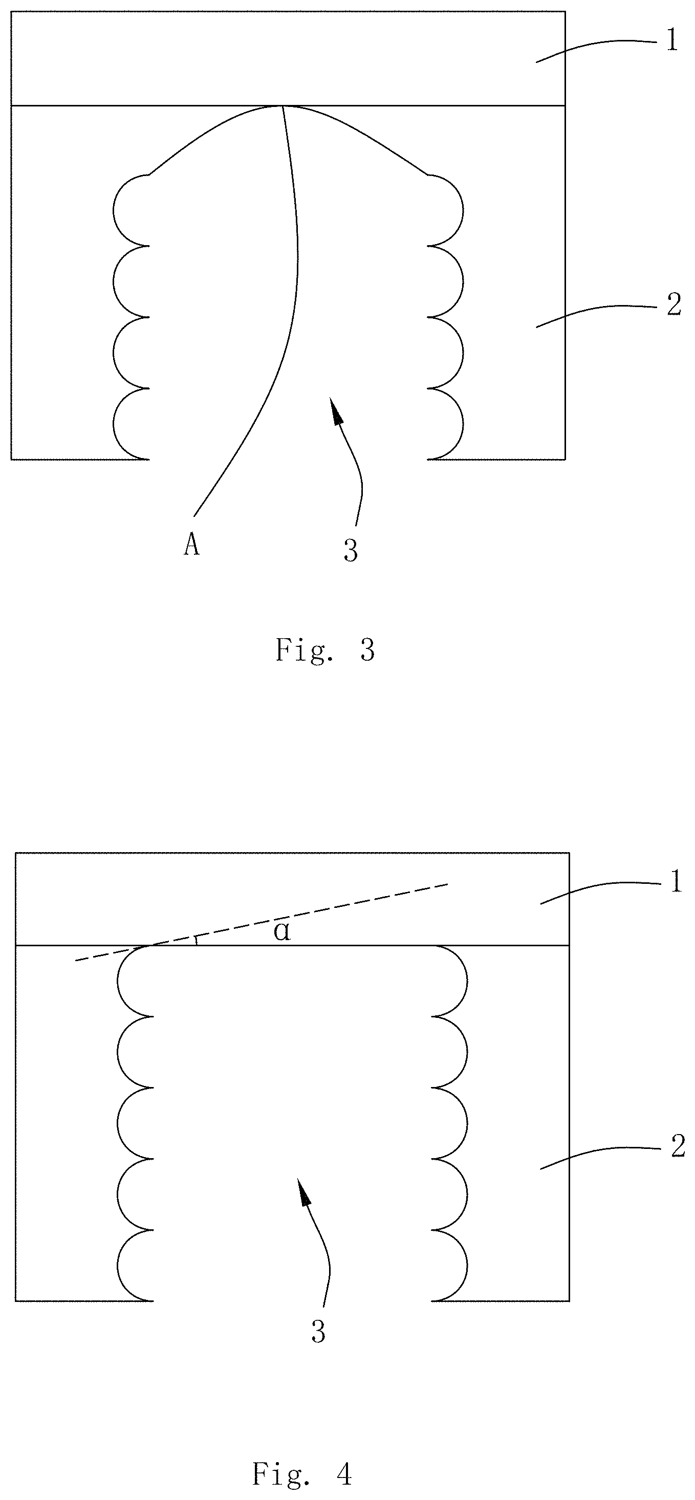
FIG. 3 is an illustration of the substrate after a main etching process.
FIG. 4 is an illustration of the substrate after an etching process.
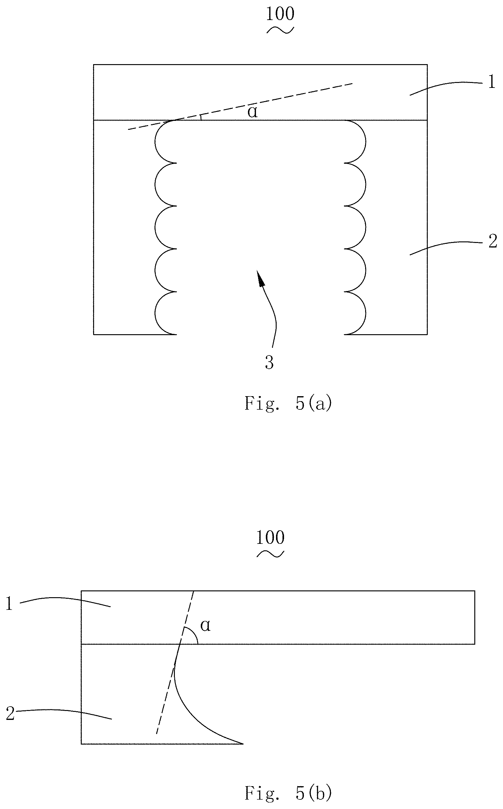
FIG. 5(a) is an illustration of a MEMS structure of the MEMS microphone.
FIG. 5(b) is another illustration of the MEMS structure of the MEMS microphone.
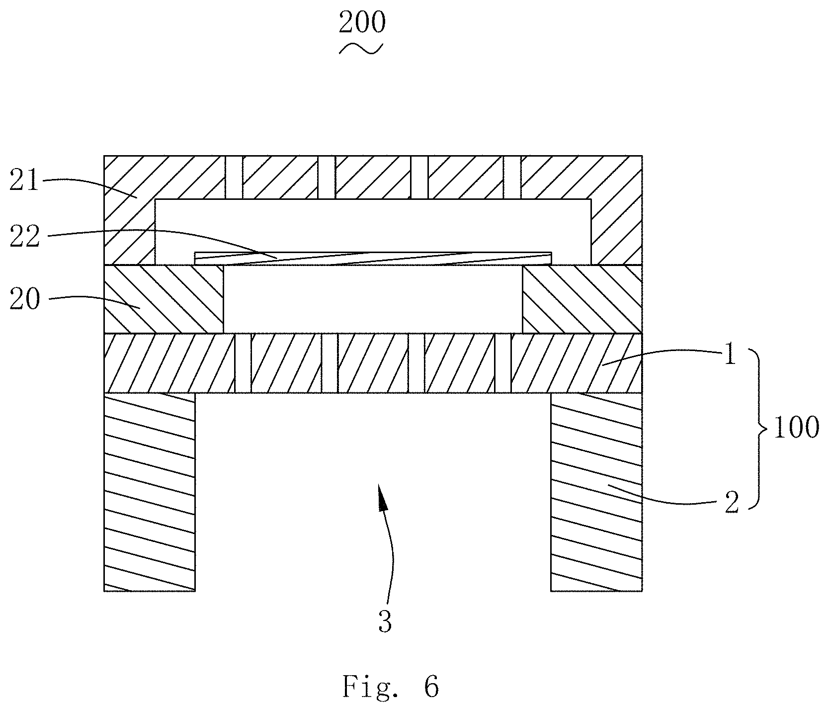
FIG. 6 is an illustration of the MEMS microphone.
DETAILED DESCRIPTION OF THE EXEMPLARY EMBODIMENTS
The present disclosure is hereinafter described in detail with reference to several exemplary embodiments. To make the technical problems to be solved, technical solutions and beneficial effects of the present disclosure more apparent, the present disclosure is described in further detail together with the figure and the embodiments. It should be understood the specific embodiments described hereby is only to explain the disclosure, not intended to limit the disclosure.
Referring to FIG. 1, an embodiment of the invention provides a manufacturing method for a MEMS structure, which comprises of the following steps:
S1. Provide a substrate, including a structural layer 1 and a silicon-based layer 2 overlapped with the structural layer 1 (as shown in FIG. 2).
Wherein, the structural layer 1 can be made from silicon, nitride, polysilicon and other materials.
S2. Carry out a main etching process. Etch out a cavity hole 3 from the end of the silicon-based layer 2, which is far away from the structural layer 1, in the direction to the structural layer 1 until the cavity hole 3 contacts the structural layer 1, as shown in FIG. 3.
Wherein, once the deepest part A of the cavity hole 3 contacts the structural layer 1, the main etching process ends.
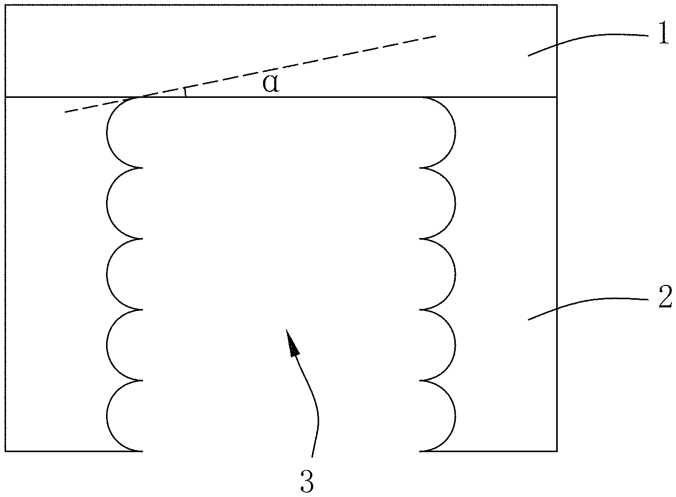
S3. Carry out an over-etching process. Deepen the cavity hole 3 and control an included angle .alpha. between a side wall of the cavity hole 3 and the structural layer 1 to be larger than 10.degree. but smaller than 90.degree., as shown in FIG. 4.
In the invention, the cavity hole 3 is deeper than 100 .mu.m.
The included angle .alpha. between the cavity hole 3 and the structural layer 1 can be controlled by controlling the etching rate, etc, in the over-etching process.
Both of S2 and S3 use Bosch process for etching. Of course, the Bosch process is not necessary. However, the Bosch process is preferred in the preferred embodiments of the invention so as to both get high verticality of the side wall and ensure the etching rate.
It should be noted that in S2, the main etching process includes the circulation operation of etching and deposition of a protection layer. In S3, the over-etching process also includes the circulation operation of etching and deposition of the protection layer.
As shown in FIG. 5, the invention also provides a MEMS structure 100 which comprises of a structural layer 1 and a silicon-based layer 2, wherein, the silicon-based layer 2 is provided with the cavity hole 3 which penetrates the silicon-based layer 2. The cavity hole 3 is deeper than 100 .mu.m. The included angle .alpha. between the cavity hole 3 and the structural layer 1 is larger than 10.degree. but smaller than 90.degree.. It has to explain that the cavity hole is a closed hole with a closed side wall, as shown in FIG. 5(a). The cavity hole 3 can also be a non-closed hole of which the side wall is not closed, as shown in FIG. 5(b). Wherein, FIG. 5(a) shows the specific structure of the MEMS structure 100 when the included angle is close to 10.degree., and FIG. 5(b) shows the specific structure of the MEMS structure 100 when the included angle is close to 90.degree.. When the included angle is between 10.degree. to 90.degree., the MEMS structure 100 has high reliability.
It has to explain that the included angle .alpha. above is the included angle between the plane where the structural layer 1 is and the tangent line of the side wall of the intersection of the structural layer 1 and the cavity hole 3.
Please refer to FIG. 6; the invention also provides a silicon microphone 200 which uses the MEMS structure 100. When the MEMS structure 100 is applied in the silicon microphone, the structural layer 1 can be used as a back plate or a diaphragm. In the specific embodiments provided by the invention, the structural layer 1 is used as a first back plate, the silicon microphone 200 also comprises of an insulation layer 20 arranged on the structural layer 1, a second back plate 21 arranged on the insulation layer 20 and a diaphragm 22 included between the second back plate 21 and the insulation layer 20.
Compared with the prior art, the manufacturing method of MEMS structure, the MEMS structure and the silicon microphone which are provided by the invention have the following advantage: the structural reliability of the microphone is effectively improved by controlling the included angle between the side wall of the cavity hole and the structural layer to be larger than 10.degree. but smaller than 90.degree..
One of ordinary skill in the art understands that the above embodiments are specific embodiments for the realization of the present invention, and in practical applications, various changes can be made to them in form and detail without deviating from the spirit and scope of the invention.
It is to be understood, however, that even though numerous characteristics and advantages of the present exemplary embodiments have been set forth in the foregoing description, together with details of the structures and functions of the embodiments, the disclosure is illustrative only, and changes may be made in detail, especially in matters of shape, size, and arrangement of parts within the principles of the invention to the full extent indicated by the broad general meaning of the terms where the appended claims are expressed.
* * * * *
D00000
D00001
D00002
D00003
D00004
XML
uspto.report is an independent third-party trademark research tool that is not affiliated, endorsed, or sponsored by the United States Patent and Trademark Office (USPTO) or any other governmental organization. The information provided by uspto.report is based on publicly available data at the time of writing and is intended for informational purposes only.
While we strive to provide accurate and up-to-date information, we do not guarantee the accuracy, completeness, reliability, or suitability of the information displayed on this site. The use of this site is at your own risk. Any reliance you place on such information is therefore strictly at your own risk.
All official trademark data, including owner information, should be verified by visiting the official USPTO website at www.uspto.gov. This site is not intended to replace professional legal advice and should not be used as a substitute for consulting with a legal professional who is knowledgeable about trademark law.