Card edge connector for an imaging sensor
Henley , et al. February 2, 2
U.S. patent number 10,911,649 [Application Number 16/140,125] was granted by the patent office on 2021-02-02 for card edge connector for an imaging sensor. This patent grant is currently assigned to DePuy Synthes Products, Inc.. The grantee listed for this patent is DePuy Synthes Products, Inc.. Invention is credited to Laurent Blanquart, Brian Dean, Jeremiah D. Henley.


| United States Patent | 10,911,649 |
| Henley , et al. | February 2, 2021 |
Card edge connector for an imaging sensor
Abstract
The disclosure extends to devices, systems and methods for connecting one or more sensors to one or more printed circuit boards (PCB) in the distal end or tip of a scope. The disclosure also extends to a connector assembly for an image sensor for protecting the sensor and conveying information from the sensor to the PCB.
| Inventors: | Henley; Jeremiah D. (Salt Lake City, UT), Blanquart; Laurent (Westlake Village, CA), Dean; Brian (Salt Lake City, UT) | ||||||||||
|---|---|---|---|---|---|---|---|---|---|---|---|
| Applicant: |
|
||||||||||
| Assignee: | DePuy Synthes Products, Inc.
(Raynham, MA) |
||||||||||
| Family ID: | 1000005338899 | ||||||||||
| Appl. No.: | 16/140,125 | ||||||||||
| Filed: | September 24, 2018 |
Prior Publication Data
| Document Identifier | Publication Date | |
|---|---|---|
| US 20190028621 A1 | Jan 24, 2019 | |
Related U.S. Patent Documents
| Application Number | Filing Date | Patent Number | Issue Date | ||
|---|---|---|---|---|---|
| 14666210 | Sep 25, 2018 | 10084944 | |||
| 61968959 | Mar 21, 2014 | ||||
| Current U.S. Class: | 1/1 |
| Current CPC Class: | A61B 1/051 (20130101); H04N 5/2253 (20130101); H04N 5/2256 (20130101); A61B 1/00124 (20130101); H04N 2005/2255 (20130101) |
| Current International Class: | H04N 5/225 (20060101); A61B 1/00 (20060101); A61B 1/05 (20060101) |
References Cited [Referenced By]
U.S. Patent Documents
| 3666885 | May 1972 | Hemsley et al. |
| 4011403 | March 1977 | Epstein et al. |
| 4363963 | December 1982 | Ando |
| 4433675 | February 1984 | Konoshima |
| 4436095 | March 1984 | Kruger |
| 4473839 | September 1984 | Noda |
| 4644403 | February 1987 | Sakai et al. |
| 4651226 | March 1987 | Motoori et al. |
| 4692606 | September 1987 | Sakai et al. |
| 4740837 | April 1988 | Yanagisawa et al. |
| 4741327 | May 1988 | Yabe |
| 4742388 | May 1988 | Cooper et al. |
| 4745471 | May 1988 | Takamura et al. |
| 4773396 | September 1988 | Okazaki |
| 4782386 | November 1988 | Ams et al. |
| 4786965 | November 1988 | Yabe |
| 4832003 | May 1989 | Yabe |
| 4845555 | July 1989 | Yabe et al. |
| 4853772 | August 1989 | Kikuchi |
| 4853773 | August 1989 | Hibino et al. |
| 4866526 | September 1989 | Ams et al. |
| 4884133 | November 1989 | Kanno et al. |
| 4884134 | November 1989 | Tsuji et al. |
| 4908701 | March 1990 | Udagawa |
| 4918521 | April 1990 | Yabe et al. |
| 4924856 | May 1990 | Noguchi |
| 4938205 | July 1990 | Nudelman |
| 4942473 | July 1990 | Zeevi et al. |
| 4947246 | August 1990 | Kikuchi |
| 4953539 | September 1990 | Nakamura et al. |
| 4959710 | September 1990 | Uehara et al. |
| 5001556 | March 1991 | Nakamura et al. |
| 5016975 | May 1991 | Sasaki et al. |
| 5021888 | June 1991 | Kondou et al. |
| 5047846 | September 1991 | Uchiyama et al. |
| RE33854 | March 1992 | Adair |
| 5103497 | April 1992 | Hicks |
| 5111804 | May 1992 | Funakoshi |
| 5133035 | July 1992 | Hicks |
| 5187572 | February 1993 | Nakamura et al. |
| 5188094 | February 1993 | Adair |
| 5196938 | March 1993 | Blessinger |
| 5200838 | April 1993 | Nudelman et al. |
| 5220198 | June 1993 | Tsuji |
| 5228430 | July 1993 | Sakamoto |
| 5233416 | August 1993 | Inoue |
| 5241170 | August 1993 | Field, Jr. et al. |
| 5255087 | October 1993 | Nakamura et al. |
| 5264925 | November 1993 | Shipp et al. |
| 5313306 | May 1994 | Kuban et al. |
| 5325847 | July 1994 | Matsuno |
| 5365268 | November 1994 | Minami |
| 5402768 | April 1995 | Adair |
| 5408268 | April 1995 | Shipp |
| 5411020 | May 1995 | Ito |
| 5427087 | June 1995 | Ito et al. |
| 5454366 | October 1995 | Ito et al. |
| 5494483 | February 1996 | Adair |
| 5523786 | June 1996 | Parulski |
| 5550595 | August 1996 | Hannah |
| 5594497 | January 1997 | Ahern et al. |
| 5665959 | September 1997 | Fossum et al. |
| 5704836 | January 1998 | Norton et al. |
| 5730702 | March 1998 | Tanaka et al. |
| 5734418 | March 1998 | Danna |
| 5748234 | May 1998 | Lippincott |
| 5749830 | May 1998 | Kaneko et al. |
| 5754313 | May 1998 | Pelchy et al. |
| 5783909 | July 1998 | Hochstein |
| 5784099 | July 1998 | Lippincott |
| 5857963 | January 1999 | Pelchy et al. |
| 5887049 | March 1999 | Fossum |
| 5929901 | July 1999 | Adair et al. |
| 5949483 | September 1999 | Fossum et al. |
| 5986693 | November 1999 | Adair et al. |
| 6023315 | February 2000 | Harrold et al. |
| 6038067 | March 2000 | George |
| 6043839 | March 2000 | Adair et al. |
| 6139489 | October 2000 | Wampler et al. |
| 6141505 | October 2000 | Miyata |
| 6142930 | November 2000 | Ito et al. |
| 6166768 | December 2000 | Fossum et al. |
| 6184922 | February 2001 | Saito et al. |
| 6184940 | February 2001 | Sano |
| 6215517 | March 2001 | Takahashi et al. |
| 6222175 | April 2001 | Krymski |
| 6239456 | May 2001 | Berezin et al. |
| 6272269 | August 2001 | Naum |
| 6275255 | August 2001 | Adair et al. |
| 6292220 | September 2001 | Ogawa et al. |
| 6294775 | September 2001 | Seibel et al. |
| 6310642 | October 2001 | Adair et al. |
| 6320331 | November 2001 | Iida et al. |
| 6331156 | December 2001 | Haefele et al. |
| 6389205 | May 2002 | Muckner et al. |
| 6416463 | July 2002 | Tsuzuki et al. |
| 6429953 | August 2002 | Feng |
| 6444970 | September 2002 | Barbato |
| 6445022 | September 2002 | Barna et al. |
| 6445139 | September 2002 | Marshall et al. |
| 6464633 | October 2002 | Hosoda et al. |
| 6466618 | October 2002 | Messing et al. |
| 6485414 | November 2002 | Neuberger |
| 6512280 | January 2003 | Chen et al. |
| 6567115 | May 2003 | Miyashita et al. |
| 6627474 | September 2003 | Barna et al. |
| 6631230 | October 2003 | Campbell |
| 6659940 | December 2003 | Adler |
| 6665013 | December 2003 | Fossum et al. |
| 6677992 | January 2004 | Matsumoto et al. |
| 6687534 | February 2004 | Tsujita |
| 6690466 | February 2004 | Miller et al. |
| 6692431 | February 2004 | Kazakevich |
| 6707499 | March 2004 | Kung et al. |
| 6772181 | August 2004 | Fu et al. |
| 6773392 | August 2004 | Kikuchi et al. |
| 6791739 | September 2004 | Ramanujan et al. |
| 6796939 | September 2004 | Hirata et al. |
| 6799065 | September 2004 | Niemeyer |
| 6809358 | October 2004 | Hsieh et al. |
| 6838653 | January 2005 | Campbell et al. |
| 6841947 | January 2005 | Berg-johansen |
| 6847399 | January 2005 | Ang |
| 6856712 | February 2005 | Fauver et al. |
| 6873363 | March 2005 | Barna et al. |
| 6879340 | April 2005 | Chevallier |
| 6899675 | May 2005 | Cline et al. |
| 6900829 | May 2005 | Orzawa et al. |
| 6906745 | June 2005 | Fossum et al. |
| 6921920 | July 2005 | Kazakevich |
| 6933974 | August 2005 | Lee |
| 6947090 | September 2005 | Komoro et al. |
| 6961461 | November 2005 | MacKinnon et al. |
| 6970195 | November 2005 | Bidermann et al. |
| 6977733 | December 2005 | Denk et al. |
| 6982740 | January 2006 | Adair et al. |
| 6998594 | February 2006 | Gaines et al. |
| 6999118 | February 2006 | Suzuki |
| 7009634 | March 2006 | Iddan et al. |
| 7009648 | March 2006 | Lauxtermann et al. |
| 7030904 | April 2006 | Adair et al. |
| 7037259 | May 2006 | Hakamata et al. |
| 7068878 | June 2006 | Crossman-Bosworth et al. |
| 7071979 | July 2006 | Ohtani et al. |
| 7079178 | July 2006 | Hynecek |
| 7102682 | September 2006 | Baer |
| 7105371 | September 2006 | Fossum et al. |
| 7106377 | September 2006 | Bean et al. |
| 7119839 | October 2006 | Mansoorian |
| 7151568 | December 2006 | Kawachi et al. |
| 7159782 | January 2007 | Johnston et al. |
| 7184084 | February 2007 | Glenn |
| 7189226 | March 2007 | Auld et al. |
| 7189961 | March 2007 | Johnston et al. |
| 7208983 | April 2007 | Imaizumi et al. |
| 7252236 | August 2007 | Johnston et al. |
| 7258663 | August 2007 | Doguchi et al. |
| 7261687 | August 2007 | Yang |
| 7280139 | October 2007 | Pahr et al. |
| 7298938 | November 2007 | Johnston |
| 7312879 | December 2007 | Johnston |
| 7319478 | January 2008 | Dolt et al. |
| 7355155 | April 2008 | Wang |
| 7356198 | April 2008 | Chauville et al. |
| 7365768 | April 2008 | Ono et al. |
| 7369140 | May 2008 | King et al. |
| 7369176 | May 2008 | Sonnenschein et al. |
| 7455638 | November 2008 | Ogawa et al. |
| 7470229 | December 2008 | Ogawa et al. |
| 7476197 | January 2009 | Wiklof et al. |
| 7532760 | May 2009 | Kaplinsky et al. |
| 7540645 | May 2009 | Choi |
| 7544163 | June 2009 | MacKinnon et al. |
| 7545434 | June 2009 | Bean et al. |
| 7564935 | July 2009 | Suzuki |
| 7567291 | July 2009 | Bechtel et al. |
| 7573516 | August 2009 | Krymski et al. |
| 7573519 | August 2009 | Phan et al. |
| 7583872 | September 2009 | Seibel et al. |
| 7616238 | November 2009 | Avni et al. |
| 7630008 | December 2009 | Sarwari |
| 7744528 | June 2010 | Wallace et al. |
| 7783133 | August 2010 | Dunki-Jacobs et al. |
| 7784697 | August 2010 | Johnston et al. |
| 7791009 | September 2010 | Johnston et al. |
| 7792378 | September 2010 | Liege et al. |
| 7794394 | September 2010 | Frangioni |
| 7813538 | October 2010 | Carroll et al. |
| 7901974 | March 2011 | Venezia et al. |
| 7914447 | March 2011 | Kanai |
| 7916193 | March 2011 | Fossum |
| 7935050 | May 2011 | Luanava et al. |
| 7944566 | May 2011 | Xie |
| 7952096 | May 2011 | Rhodes |
| 7969097 | June 2011 | Van De Ven |
| 7995123 | August 2011 | Lee et al. |
| 8040394 | October 2011 | Fossum et al. |
| 8054339 | November 2011 | Fossum et al. |
| 8059174 | November 2011 | Mann et al. |
| 8100826 | January 2012 | MacKinnon et al. |
| 8159584 | April 2012 | Iwabuchi et al. |
| 8193542 | June 2012 | Machara |
| 8212884 | July 2012 | Seibel et al. |
| 8231522 | July 2012 | Endo et al. |
| 8300111 | October 2012 | Iwane |
| 8372003 | February 2013 | St. George et al. |
| 8382662 | February 2013 | Soper et al. |
| 8396535 | March 2013 | Wang et al. |
| 8423110 | April 2013 | Barbato et al. |
| 8471938 | June 2013 | Altice, Jr. et al. |
| 8476575 | July 2013 | Mokhuatyuk |
| 8482823 | July 2013 | Cheng |
| 8493474 | July 2013 | Richardson |
| 8493564 | July 2013 | Brukilacchio et al. |
| 8523367 | September 2013 | Ogura |
| 8537203 | September 2013 | Seibel et al. |
| 8559743 | October 2013 | Liege et al. |
| 8582011 | November 2013 | Dosluoglu |
| 8602971 | December 2013 | Farr |
| 8605177 | December 2013 | Rossi et al. |
| 8610808 | December 2013 | Prescher et al. |
| 8614754 | December 2013 | Fossum |
| 8625016 | January 2014 | Fossum et al. |
| 8638847 | January 2014 | Wang |
| 8648287 | February 2014 | Fossum |
| 8649848 | February 2014 | Crane et al. |
| 8668339 | March 2014 | Kabuki et al. |
| 8675125 | March 2014 | Cossairt et al. |
| 8698887 | April 2014 | Makino et al. |
| 8836834 | September 2014 | Hashimoto et al. |
| 8848063 | September 2014 | Jo et al. |
| 8858425 | October 2014 | Farr et al. |
| 8885034 | November 2014 | Adair et al. |
| 9182337 | November 2015 | Kamee et al. |
| 9349764 | May 2016 | Lee et al. |
| 9509917 | November 2016 | Blanquart et al. |
| 9516239 | December 2016 | Blanquart et al. |
| 9634878 | April 2017 | Bench |
| 9762879 | September 2017 | Blanquart et al. |
| 9777913 | October 2017 | Talbert et al. |
| 10084944 | September 2018 | Henley et al. |
| 10251530 | April 2019 | Henley et al. |
| 10277875 | April 2019 | Blanquart et al. |
| 2001/0016064 | August 2001 | Tsuruoka et al. |
| 2001/0017649 | August 2001 | Yaron |
| 2001/0030744 | October 2001 | Chang |
| 2001/0055462 | December 2001 | Seibel |
| 2002/0054219 | May 2002 | Jaspers |
| 2002/0064341 | May 2002 | Fauver et al. |
| 2002/0080248 | June 2002 | Adair et al. |
| 2002/0080359 | June 2002 | Denk et al. |
| 2002/0140844 | October 2002 | Kurokawa et al. |
| 2002/0158976 | October 2002 | Vni et al. |
| 2002/0158986 | October 2002 | Baer |
| 2003/0007087 | January 2003 | Hakamata et al. |
| 2003/0007686 | January 2003 | Roever |
| 2003/0107664 | June 2003 | Suzuki |
| 2003/0189663 | October 2003 | Dolt et al. |
| 2003/0189705 | October 2003 | Pardo |
| 2004/0082833 | April 2004 | Adler et al. |
| 2004/0170712 | September 2004 | Sadek El Mogy |
| 2005/0009982 | January 2005 | Inagaki et al. |
| 2005/0027164 | February 2005 | Barbato et al. |
| 2005/0038322 | February 2005 | Banik |
| 2005/0041571 | February 2005 | Ichihara et al. |
| 2005/0113641 | May 2005 | Bala |
| 2005/0122530 | June 2005 | Denk et al. |
| 2005/0151866 | July 2005 | Ando et al. |
| 2005/0200291 | September 2005 | Naugler, Jr. et al. |
| 2005/0234302 | October 2005 | MacKinnon et al. |
| 2005/0237384 | October 2005 | Jess et al. |
| 2005/0261552 | November 2005 | Mori et al. |
| 2005/0267328 | December 2005 | Blumzvig |
| 2005/0267329 | December 2005 | Konstorum |
| 2005/0277808 | December 2005 | Sonnenschein |
| 2005/0288546 | December 2005 | Sonnenschein et al. |
| 2006/0038823 | February 2006 | Arcas |
| 2006/0069314 | March 2006 | Farr |
| 2006/0087841 | April 2006 | Chern et al. |
| 2006/0197664 | September 2006 | Zhang et al. |
| 2006/0202036 | September 2006 | Wang et al. |
| 2006/0221250 | October 2006 | Rossbach et al. |
| 2006/0226231 | October 2006 | Johnston et al. |
| 2006/0264734 | November 2006 | Kimoto et al. |
| 2006/0274335 | December 2006 | Wittenstein |
| 2007/0010712 | January 2007 | Negishi |
| 2007/0029629 | February 2007 | Yazdi |
| 2007/0041448 | February 2007 | Miller et al. |
| 2007/0083085 | April 2007 | Birnkrant et al. |
| 2007/0129601 | June 2007 | Johnston et al. |
| 2007/0147033 | June 2007 | Ogawa et al. |
| 2007/0182723 | August 2007 | Imai et al. |
| 2007/0182842 | August 2007 | Sonnenschein |
| 2007/0225560 | September 2007 | Avni et al. |
| 2007/0244364 | October 2007 | Luanava et al. |
| 2007/0244365 | October 2007 | Wiklof |
| 2007/0276187 | November 2007 | Wiklof et al. |
| 2007/0279486 | December 2007 | Bayer et al. |
| 2007/0285526 | December 2007 | Mann et al. |
| 2007/0293720 | December 2007 | Bayer |
| 2008/0045800 | February 2008 | Farr |
| 2008/0049132 | February 2008 | Suzuki |
| 2008/0088719 | April 2008 | Jacob et al. |
| 2008/0107333 | May 2008 | Mazinani et al. |
| 2008/0136953 | June 2008 | Barnea et al. |
| 2008/0158348 | July 2008 | Karpen et al. |
| 2008/0164550 | July 2008 | Chen et al. |
| 2008/0165360 | July 2008 | Johnston |
| 2008/0192131 | August 2008 | Kim et al. |
| 2008/0218598 | September 2008 | Harada et al. |
| 2008/0218615 | September 2008 | Huang et al. |
| 2008/0218824 | September 2008 | Johnston et al. |
| 2008/0249369 | October 2008 | Seibel et al. |
| 2009/0012361 | January 2009 | MacKinnon et al. |
| 2009/0012368 | January 2009 | Banik |
| 2009/0021588 | January 2009 | Border et al. |
| 2009/0021618 | January 2009 | Schwarz |
| 2009/0024000 | January 2009 | Chen |
| 2009/0028465 | January 2009 | Pan |
| 2009/0074265 | March 2009 | Huang |
| 2009/0091645 | April 2009 | Trimeche et al. |
| 2009/0137893 | May 2009 | Seibel et al. |
| 2009/0147077 | June 2009 | Tani et al. |
| 2009/0154886 | June 2009 | Lewis et al. |
| 2009/0160976 | June 2009 | Chen et al. |
| 2009/0189530 | July 2009 | Ashdown et al. |
| 2009/0208143 | August 2009 | Yoon et al. |
| 2009/0227847 | September 2009 | Tepper et al. |
| 2009/0232213 | September 2009 | Jia |
| 2009/0259102 | October 2009 | Koninckx et al. |
| 2009/0268063 | October 2009 | Ellis-Monaghan et al. |
| 2009/0274380 | November 2009 | Wedi |
| 2009/0292168 | November 2009 | Farr |
| 2009/0309500 | December 2009 | Reisch |
| 2009/0316116 | December 2009 | Melville et al. |
| 2009/0322912 | December 2009 | Blanquart |
| 2010/0026722 | February 2010 | Kondo |
| 2010/0049180 | February 2010 | Wells et al. |
| 2010/0069713 | March 2010 | Endo et al. |
| 2010/0102199 | April 2010 | Negley et al. |
| 2010/0121142 | May 2010 | OuYang et al. |
| 2010/0121143 | May 2010 | Sugimoto et al. |
| 2010/0123775 | May 2010 | Shibasaki |
| 2010/0134608 | June 2010 | Shibasaki |
| 2010/0134662 | June 2010 | Bub |
| 2010/0135398 | June 2010 | Wittmann et al. |
| 2010/0137684 | June 2010 | Shibasaki et al. |
| 2010/0149421 | June 2010 | Lin et al. |
| 2010/0157037 | June 2010 | Iketani et al. |
| 2010/0157039 | June 2010 | Sugai |
| 2010/0165087 | July 2010 | Corso et al. |
| 2010/0171429 | July 2010 | Garcia et al. |
| 2010/0182446 | July 2010 | Matsubayashi |
| 2010/0198009 | August 2010 | Farr et al. |
| 2010/0198134 | August 2010 | Eckhouse et al. |
| 2010/0201797 | August 2010 | Shizukuishi et al. |
| 2010/0208056 | August 2010 | Olsson |
| 2010/0228089 | September 2010 | Hoffman et al. |
| 2010/0261961 | October 2010 | Scoff et al. |
| 2010/0274082 | October 2010 | Iguchi et al. |
| 2010/0274090 | October 2010 | Ozaki et al. |
| 2010/0305406 | December 2010 | Braun et al. |
| 2010/0309333 | December 2010 | Smith et al. |
| 2011/0028790 | February 2011 | Farr et al. |
| 2011/0034769 | February 2011 | Adair et al. |
| 2011/0051390 | March 2011 | Lin et al. |
| 2011/0063483 | March 2011 | Rossi et al. |
| 2011/0122301 | May 2011 | Yamura et al. |
| 2011/0149358 | June 2011 | Cheng |
| 2011/0181709 | July 2011 | Wright et al. |
| 2011/0181840 | July 2011 | Cobb |
| 2011/0184239 | July 2011 | Wright et al. |
| 2011/0184243 | July 2011 | Wright et al. |
| 2011/0208004 | August 2011 | Feingold et al. |
| 2011/0212649 | September 2011 | Stokoe et al. |
| 2011/0237882 | September 2011 | Saito |
| 2011/0237884 | September 2011 | Saito |
| 2011/0245605 | October 2011 | Jacobsen et al. |
| 2011/0245616 | October 2011 | Kobayashi |
| 2011/0255844 | October 2011 | Wu et al. |
| 2011/0274175 | November 2011 | Sumitomo |
| 2011/0279679 | November 2011 | Samuel et al. |
| 2011/0288374 | November 2011 | Hadani et al. |
| 2011/0291564 | December 2011 | Huang |
| 2011/0292258 | December 2011 | Adler et al. |
| 2011/0295061 | December 2011 | Haramaty et al. |
| 2012/0004508 | January 2012 | McDowall et al. |
| 2012/0014563 | January 2012 | Bendall |
| 2012/0029279 | February 2012 | Kucklick |
| 2012/0033118 | February 2012 | Lee et al. |
| 2012/0041267 | February 2012 | Benning et al. |
| 2012/0041534 | February 2012 | Clerc et al. |
| 2012/0050592 | March 2012 | Oguma |
| 2012/0078052 | March 2012 | Cheng |
| 2012/0098933 | April 2012 | Robinson et al. |
| 2012/0104230 | May 2012 | Eismann et al. |
| 2012/0113506 | May 2012 | Gmitro et al. |
| 2012/0120282 | May 2012 | Goris |
| 2012/0140302 | June 2012 | Xie et al. |
| 2012/0155761 | June 2012 | Matsuoka |
| 2012/0157774 | June 2012 | Kaku |
| 2012/0172665 | July 2012 | Allyn |
| 2012/0194686 | August 2012 | Liu et al. |
| 2012/0197080 | August 2012 | Murayama |
| 2012/0200685 | August 2012 | Kawasaki et al. |
| 2012/0209071 | August 2012 | Bayer |
| 2012/0242975 | September 2012 | Min et al. |
| 2012/0262621 | October 2012 | Sato et al. |
| 2012/0281111 | November 2012 | Jo et al. |
| 2012/0319586 | December 2012 | Riesebosch |
| 2012/0327270 | December 2012 | Shirakawa et al. |
| 2013/0018256 | January 2013 | Kislev et al. |
| 2013/0035545 | February 2013 | Ono |
| 2013/0053642 | February 2013 | Mizuyoshi et al. |
| 2013/0070071 | March 2013 | Peltie et al. |
| 2013/0126708 | May 2013 | Blanquart |
| 2013/0127934 | May 2013 | Chiang |
| 2013/0135589 | May 2013 | Curtis et al. |
| 2013/0144120 | June 2013 | Yamazaki |
| 2013/0155215 | June 2013 | Shimada et al. |
| 2013/0155305 | June 2013 | Shintani |
| 2013/0158346 | June 2013 | Soper et al. |
| 2013/0184524 | July 2013 | Shimada et al. |
| 2013/0211217 | August 2013 | Yamaguchi et al. |
| 2013/0242069 | September 2013 | Kobayashi |
| 2013/0244453 | September 2013 | Sakamoto |
| 2013/0274597 | October 2013 | Byrne et al. |
| 2013/0292571 | November 2013 | Mukherjee et al. |
| 2013/0296652 | November 2013 | Farr |
| 2013/0300837 | November 2013 | DiCarlo et al. |
| 2013/0342690 | December 2013 | Williams et al. |
| 2014/0022365 | January 2014 | Yoshino |
| 2014/0031623 | January 2014 | Kagaya |
| 2014/0005532 | February 2014 | Choi et al. |
| 2014/0052004 | February 2014 | D'Alfonso et al. |
| 2014/0066711 | March 2014 | Farin |
| 2014/0073852 | March 2014 | Banik et al. |
| 2014/0073853 | March 2014 | Swisher et al. |
| 2014/0078278 | March 2014 | Lei |
| 2014/0088363 | March 2014 | Sakai et al. |
| 2014/0104466 | April 2014 | Fossum |
| 2014/0110485 | April 2014 | Toa |
| 2014/0142383 | May 2014 | Blunnenzweig; Ade |
| 2014/0160318 | June 2014 | Blanquart et al. |
| 2014/0163319 | June 2014 | Blanquart et al. |
| 2014/0198249 | July 2014 | Tanaka et al. |
| 2014/0203084 | July 2014 | Wang |
| 2014/0225215 | August 2014 | Chien |
| 2014/0267655 | September 2014 | Richardson et al. |
| 2014/0267851 | September 2014 | Rhoads |
| 2014/0267890 | September 2014 | Lelescu et al. |
| 2014/0268860 | September 2014 | Talbert et al. |
| 2014/0275764 | September 2014 | Shen et al. |
| 2014/0288365 | September 2014 | Henley et al. |
| 2014/0300698 | October 2014 | Wany |
| 2014/0316197 | October 2014 | St. George et al. |
| 2014/0316199 | October 2014 | Kucklick |
| 2014/0354788 | December 2014 | Yano |
| 2014/0364689 | December 2014 | Adair |
| 2015/0237245 | August 2015 | Renard |
| 2015/0271370 | September 2015 | Henley et al. |
| 2016/0183775 | June 2016 | Blanquart et al. |
| 2017/0085853 | March 2017 | Blanquart et al. |
| 2017/0230574 | August 2017 | Richardson et al. |
| 2019/0028621 | January 2019 | Henley et al. |
| 2019/0133416 | May 2019 | Henley et al. |
| 2019/0174058 | June 2019 | Richardson et al. |
| 2019/0253685 | August 2019 | Blanquart et al. |
| 1520696 | Aug 2004 | CN | |||
| 101079966 | Nov 2007 | CN | |||
| 201239130 | May 2009 | CN | |||
| 101449575 | Jun 2009 | CN | |||
| 101634749 | Jan 2010 | CN | |||
| 101755448 | Jun 2010 | CN | |||
| 102469932 | May 2012 | CN | |||
| 103185960 | Jul 2013 | CN | |||
| 0660616 | Jun 1995 | EP | |||
| 0904725 | Mar 1999 | EP | |||
| 1079255 | Feb 2001 | EP | |||
| 1116473 | Jul 2001 | EP | |||
| 1637062 | Mar 2006 | EP | |||
| 1712177 | Oct 2006 | EP | |||
| 1819151 | Aug 2007 | EP | |||
| 2359739 | Aug 2011 | EP | |||
| 2371268 | Aug 2011 | EP | |||
| 3459431 | Mar 2014 | EP | |||
| H04-039789 | Apr 1992 | JP | |||
| H07-240931 | Sep 1995 | JP | |||
| 1995-240931 | Mar 1997 | JP | |||
| 2000-051150 | Feb 2000 | JP | |||
| 2000-199863 | Jul 2000 | JP | |||
| 2000270230 | Sep 2000 | JP | |||
| 2001-308531 | Nov 2001 | JP | |||
| 2002-020816 | Jan 2002 | JP | |||
| 2002-028125 | Jan 2002 | JP | |||
| 2002-045329 | Feb 2002 | JP | |||
| 2002-112961 | Apr 2002 | JP | |||
| 2005-204741 | Aug 2005 | JP | |||
| 2007-029746 | Feb 2007 | JP | |||
| 2007143963 | Jun 2007 | JP | |||
| 2007-240931 | Sep 2007 | JP | |||
| 2008514304 | May 2008 | JP | |||
| 2008-153313 | Jul 2008 | JP | |||
| 2008264539 | Nov 2008 | JP | |||
| 2008295929 | Dec 2008 | JP | |||
| 2009-537283 | Oct 2009 | JP | |||
| 2010-17377 | Jan 2010 | JP | |||
| 2010-068992 | Apr 2010 | JP | |||
| 2010-125284 | Jun 2010 | JP | |||
| 2010-158415 | Jul 2010 | JP | |||
| 2011-055327 | Mar 2011 | JP | |||
| 2011514605 | May 2011 | JP | |||
| 2012-000160 | Jan 2012 | JP | |||
| 2012024450 | Feb 2012 | JP | |||
| 2013-27432 | Feb 2013 | JP | |||
| 2011-267098 | Jun 2013 | JP | |||
| 2014514782 | Jun 2014 | JP | |||
| 5682812 | Jan 2015 | JP | |||
| 2015525642 | Sep 2015 | JP | |||
| A61-62440 | Jun 2017 | JP | |||
| 2015001195 | Jan 2016 | MX | |||
| 346174 | Mar 2017 | MX | |||
| 1996005693 | Feb 1996 | WO | |||
| 2006037034 | Apr 2006 | WO | |||
| 2009018613 | Feb 2009 | WO | |||
| 2009115885 | Sep 2009 | WO | |||
| 2009120228 | Oct 2009 | WO | |||
| 2012043771 | Apr 2012 | WO | |||
| 2012137845 | Oct 2012 | WO | |||
Other References
|
Blumenfeld, et al. Three-dimensional image registration of MR proximal femur images for the analysis of trabecular bone parameters. Oct. 2008. [retrieved on Jul. 30, 2014] Retrieved from the internet: <URL: http://www.ncbi.nlm.nih.gov/pmc/articles/PMC2673590/>. cited by applicant . Jack, Keith "Video Demystified: A Handbook for the Digital Engineer," 2007 Fifth Edition. ISBN: 978-0-7506-8395-1, p. 21. cited by applicant. |
Primary Examiner: Rahman; Mohammad J
Attorney, Agent or Firm: Edwards; Terrence J. TechLaw Ventures, PLLC
Parent Case Text
CROSS-REFERENCE TO RELATED APPLICATIONS
This application is a continuation of U.S. application Ser. No. 14/666,210, filed Mar. 23, 2015 (now U.S. Pat. No. 10,084,944, issued Sep. 25, 2018) and claims the benefit of U.S. Provisional Application No. 61/968,959, filed Mar. 21, 2014, which are incorporated herein by reference in their entirety, including but not limited to those portions that specifically appear hereinafter, the incorporation by reference being made with the following exception: In the event that any portion of the above-referenced applications are inconsistent with this application, this application supersedes said above-referenced applications.
Claims
What is claimed is:
1. A surgical scope for providing an image in a light deficient environment comprising: a tubular member comprising a proximal portion and a distal portion; a printed circuit board; and an image sensor; a connector assembly that is located at the distal portion of the tubular member and comprising a first end that receives the image sensor, a second end having a recess for receiving the printed circuit board, and a plurality of electrical connectors between the first end and the second end for electrically connecting the printed circuit board to the image sensor; wherein the image sensor is connected to the connector assembly at the first end of said connector assembly, wherein the printed circuit board is connected to the connector assembly at the second end of said connector assembly, such that the connector assembly attaches the image sensor at the distal portion of the tubular member and electrically connects the image sensor to the printed circuit board via the plurality of electrical connectors, thereby providing electrical communication between the image sensor and the printed circuit board, and wherein the connector assembly attaches the image sensor and the printed circuit board within the tubular member such that the image sensor is disposed in an orientation that is substantially perpendicular to the printed circuit board.
2. The surgical scope of claim 1, wherein the printed circuit board is attached perpendicularly out of the center of and with respect to the image sensor.
3. The surgical scope of claim 1, wherein the printed circuit board is attached perpendicularly off of an edge of and with respect to the image sensor.
4. The surgical scope of claim 1, wherein the image sensor comprises a plurality of electrical pads that are electrically attached to the plurality of electrical connectors via wire bonds.
5. The surgical scope of claim 1, wherein the image sensor is electrically attached to one of the plurality of electrical connectors via an electrically conductive adhesive.
6. The surgical scope of claim 5, wherein the image sensor is electrically attached to the plurality of electrical connectors via wire bonds; wherein the image sensor comprises a silicon die; and wherein the electrically conductive adhesive is placed in controlled locations of the connector assembly to electrically connect a backside of the silicon die to a ground in the connector assembly.
7. The surgical scope of claim 1, wherein the image sensor is backside illuminated and comprises a plurality of electrical pads that are soldered to the plurality of electrical connectors of the connector assembly to thereby electrically attach the image sensor to the connector assembly.
8. The surgical scope of claim 1, wherein the image sensor is located above a plane of the electrical connectors at the first end of the connector assembly, such that the electrical connectors are located underneath the image sensor.
9. The surgical scope of claim 1, wherein the connector assembly comprises a cavity comprising a sidewall at the first end, wherein the image sensor is located within the cavity such that the sidewall of said cavity surrounds at least a portion of the image sensor, thereby protecting the image sensor and electrical connectors.
10. The surgical scope of claim 9, wherein the image sensor comprises a pixel array that is located above a plane of the electrical connectors at the first end of the connector assembly.
11. The surgical scope of claim 9, wherein the image sensor comprises a pixel array that is located on the same plane as the electrical connectors at the first end of the connector assembly.
12. The surgical scope of claim 9, wherein the image sensor comprises a pixel array that is located beneath a plane of the electrical connectors at the first end of the connector assembly.
13. The surgical scope of claim 1, wherein the recess comprises a slot for receiving the printed circuit board therein; and wherein the printed circuit board is held in the slot via a bias force.
14. The surgical scope of claim 13, wherein the plurality of electrical connectors extend into the slot, such that when the printed circuit board is located within the slot the electrical connectors of the connector assembly are in electrical communication with corresponding electrical connectors on the printed circuit board.
15. A system for providing an image in a light deficient environment, the system comprising: a surgical scope comprising a tubular member comprising a proximal portion and a distal portion; a light source; a camera control unit; and a display; wherein the surgical scope comprises: a printed circuit board; and an image sensor; a connector assembly that is located at the distal portion of the tubular member and comprising a first end that receives the image sensor, a second end having a recess for receiving the printed circuit board, and a plurality of electrical connectors between the first end and the second end for electrically connecting the printed circuit board to the image sensor; wherein the image sensor is connected to the connector assembly at the second end of said connector assembly, wherein the printed circuit board is connected to the connector assembly at the first end of said connector assembly, such that the connector assembly attaches the image sensor at the distal portion of the tubular member and electrically connects the image sensor to the printed circuit board via the plurality of electrical connectors, thereby providing electrical communication between the image sensor and the printed circuit board, and wherein the connector assembly attaches the image sensor and the printed circuit board within the tubular member such that the image sensor is disposed in an orientation that is substantially perpendicular to the printed circuit board.
16. The system of claim 15, wherein the printed circuit board is attached perpendicularly out of the center of and with respect to the image sensor.
17. The system of claim 15, wherein the printed circuit board is attached perpendicularly off of an edge of and with respect to the image sensor.
18. The system of claim 15, wherein the image sensor comprises a plurality of electrical pads that are electrically attached to the plurality of electrical connectors via wire bonds.
19. The system of claim 15, wherein the image sensor is electrically attached to one of the plurality of electrical connectors via an electrically conductive adhesive.
20. The system of claim 19, wherein the image sensor is electrically attached to the plurality of electrical connectors via wire bonds; wherein the image sensor comprises a silicon die; and wherein the electrically conductive adhesive is placed in controlled locations of the connector assembly to electrically connect a backside of the silicon die to a ground in the connector assembly.
21. The system of claim 15, wherein the image sensor is backside illuminated and comprises a plurality of electrical pads that are soldered to the plurality of electrical connectors of the connector assembly to thereby electrically attach the image sensor to the connector assembly.
22. The system of claim 15, wherein the image sensor is located above a plane of the electrical connectors at the first end of the connector assembly, such that the electrical connectors are located underneath the image sensor.
23. The system of claim 15, wherein the connector assembly comprises a cavity comprising a sidewall at the first end, wherein the image sensor is located within the cavity such that the sidewall of said cavity surrounds at least a portion of the image sensor, thereby protecting the image sensor and electrical connectors.
24. The system of claim 23, wherein the image sensor comprises a pixel array that is located above a plane of the electrical connectors at the first end of the connector assembly.
25. The system of claim 23, wherein the image sensor comprises a pixel array that is located on the same plane as the electrical connectors at the first end of the connector assembly.
26. The system of claim 23, wherein the image sensor comprises a pixel array that is located beneath a plane of the electrical connectors at the first end of the connector assembly.
27. The system of claim 15, wherein the recess comprises a slot for receiving the printed circuit board therein; and wherein the printed circuit board is held in the slot via a bias force.
28. The system of claim 27, wherein the plurality of electrical connectors extend into the slot, such that when the printed circuit board is located within the slot the electrical connectors of the connector assembly are in electrical communication with corresponding electrical connectors on the printed circuit board.
Description
STATEMENT REGARDING FEDERALLY SPONSORED RESEARCH OR DEVELOPMENT
Not Applicable.
BACKGROUND
The disclosure relates generally to card edge connectors and more specifically, but not entirely, to card edge connectors for sensors, such as an image sensor. Advances in technology have provided advances in imaging capabilities for medical use. One area that has enjoyed some of the most beneficial advances is that of endoscopic surgical procedures because of the advances in the components that make up an endoscope.
Conventional, digital video systems used for laparoscopy, arthroscopy, ENT, gynecology and urology are based upon conventional, rigid endoscopes, which are optically and mechanically coupled to a separate hand-piece unit, which contains one or more image sensor(s). Image information is optically transmitted along the length of the endoscope, after which it is focused upon the sensor via an optical coupler.
However, due to advances in technology sensors are now being located in the distal end or distal tip of medical or other type of scopes. With such advancements come difficulties and problems associated with mechanically and electrically connecting the sensor to a printed circuit board (PCB) in such scopes. Accordingly, devices, systems and methods for connecting sensors to PCBs in the distal end or tip of a scope are needed. As will be seen, the disclosure provides such devices, systems and methods for connecting sensors to PCBs in the distal end or tip of a scope in an effective and elegant manner.
The features and advantages of the disclosure will be set forth in the description which follows, and in part will be apparent from the description, or may be learned by the practice of the disclosure without undue experimentation. The features and advantages of the disclosure may be realized and obtained by means of the instruments and combinations particularly pointed out in the appended claims.
BRIEF DESCRIPTION OF THE DRAWINGS
Non-limiting and non-exhaustive implementations of the disclosure are described with reference to the following figures, wherein like reference numerals refer to like parts throughout the various views unless otherwise specified. Advantages of the disclosure will become better understood with regard to the following description and accompanying drawings where:
FIGS. 1A-1G illustrate various embodiments of an endoscopic system in accordance with the principles and teachings of the disclosure;
FIGS. 2A-2D illustrate front, side cross-sectional, rear, and bottom cross-sectional views, respectively, of an endoscopic device in accordance with the principles and teachings of the disclosure;
FIGS. 3A-3D illustrate front, side cross-sectional, rear, and bottom cross-sectional views, respectively, of a card edge connector device in accordance with the principles and teachings of the disclosure;
FIGS. 4A-4C illustrate front, side cross-sectional and bottom cross-sectional views, respectively, of a card edge connector device with a sensor loaded therein in accordance with the principles and teachings of the disclosure;
FIGS. 5A-5C illustrate front, side cross-sectional, and bottom cross-sectional views, respectively, of a card edge connector device with a sensor loaded therein with wire bonds connecting the sensor to electrical connectors, such as pins or pads, of the connector in accordance with the principles and teachings of the disclosure;
FIGS. 6A-6C illustrate a front perspective view of a card edge connector device, a rear perspective view of the card edge connector device, and a front perspective view of the card edge connector device with a sensor loaded therein, respectively, in accordance with the principles and teachings of the disclosure;
FIGS. 7A-7C illustrate front, side cross-sectional and bottom cross-sectional views, respectively, of a card edge connector device with a sensor loaded proud of a plane of the connector in accordance with the principles and teachings of the disclosure;
FIGS. 8A-8B illustrate perspective views of a card edge connector device for use with a backside illuminated sensor loaded proud of a plane of the connector in accordance with the principles and teachings of the disclosure;
FIGS. 9A-9C illustrate front, side cross-sectional and bottom cross-sectional views, respectively, of a card edge connector device with a sensor loaded proud of a plane of the connector in accordance with the principles and teachings of the disclosure; and
FIGS. 10A and 10B illustrate a front view and a side cross-sectional view, respectively, of a conventional, prior art packaged imaging sensor device.
DETAILED DESCRIPTION
The disclosure extends to devices, systems and methods for connecting one or more sensors to one or more printed circuit boards (PCB) in the distal end or tip of a scope where lateral space may be limited. The disclosure also extends to a card edge connector for an image sensor for protecting the sensor and conveying information from the sensor to the PCB, wherein the image sensor may be connected at one end of the card edge connector and the PCB may be connected at the opposite end of the card edge connector. The disclosure also extends to a card edge connector for an image sensor for protecting the sensor and conveying information from the sensor to the PCB, wherein the image sensor may be connected at one end of the card edge connector and the PCB may be connected at the opposite end of the card edge connector in a vertical and substantially perpendicular orientation with respect to the printed circuit board. A portion of a PCB may comprise traces leading to the edge of the board that are intended to plug into a matching card edge connector socket. The card edge connector may only require a female connector where the male connector may be formed out of the edge of the PCB.
In the following description of the disclosure, reference is made to the accompanying drawings, which form a part hereof, and in which is shown by way of illustration specific implementations in which the disclosure may be practiced. It is understood that other implementations may be utilized and structural changes may be made without departing from the scope of the disclosure.
In describing and claiming the subject matter of the disclosure, the following terminology will be used in accordance with the definitions set out below.
It must be noted that, as used in this specification and the appended claims, the singular forms "a," "an," and "the" include plural referents unless the context clearly dictates otherwise.
As used herein, the terms "comprising," "including," "containing," "characterized by," and grammatical equivalents thereof are inclusive or open-ended terms that do not exclude additional, unrecited elements or method steps.
As used herein, the term "proximal" shall refer broadly to the concept of a portion nearest an origin.
As used herein, the term "distal" shall generally refer to the opposite of proximal, and thus to the concept of a portion farther from an origin, or a furthest portion, depending upon the context.
Referring now to FIG. 1, there is illustrated various embodiments of an endoscopic system 100. It will be appreciated that the system 100 may comprise many different configurations. One example is shown in FIG. 1A, which illustrates an endoscopic system 100 comprising a rigid angled scope 102, an optical coupler 104, a handpiece 106, an image sensor 108, which may be located within the handpiece 106 or distally at a tip of the endoscope 102 as illustrated in dashed lines, an electronic cable 110, a light cable 112, such as a fiber optic cable, a light source 114, a control unit 116, such as a camera control unit (CCU), a video cable 118 and a display 120.
The system configuration shown in FIG. 1B illustrates an endoscopic system 100 comprising a rigid angled scope 102, an optical coupler 104, a handpiece 106, an image sensor 108, which may be located within the handpiece 106 or distally at a tip of the endoscope 102 as illustrated in dashed lines, an electronic cable 110, a light cable 112, such as a fiber optic cable, a control unit 116, such as a camera control unit (CCU), with an integrated light source 114, a video cable 118, and a display 120.
The system configuration shown in FIG. 1C illustrates an endoscopic system 100 comprising an articulating scope 102, an optical coupler 104, a handpiece 106, an image sensor 108, which may be located within the handpiece 106 or distally at a tip of the endoscope 102 as illustrated in dashed lines, an electronic cable 110, a light cable 112, such as a fiber optic cable, a light source 114, a control unit 116, such as a camera control unit (CCU), a video cable 118 and a display 120.
The system configuration shown in FIG. 1D illustrates an endoscopic system 100 comprising a handpiece 106 with an integrated rigid 0 degree scope 102, an image sensor 108, which may be located within the handpiece 106 or distally at a tip of the scope 102 as illustrated in dashed lines, a combined electronic and light cable 110, a control unit 116, such as a camera control unit (CCU) with an integrated light source 114, a video cable 118 and a display 120.
The system configuration shown in FIG. 1E illustrates an endoscopic system 100 comprising a handpiece 106 with an integrated rigid angled scope 102 and rotation post 105, an image sensor 108, which may be located within the handpiece 106 or distally at a tip of the scope 102 as illustrated in dashed lines, a combined electronic and light cable 110, a control unit 116, such as a camera control unit (CCU) with an integrated light source 114, a video cable 118 and a display 120.
The system configuration shown in FIG. 1F illustrates an endoscopic system 100 comprising a handpiece 106 with an integrated articulating scope 102, an image sensor 108, which may be located within the handpiece 106 or distally at a tip of the scope 102 as illustrated in dashed lines, a combined electronic and light cable 110, a control unit 116, such as a camera control unit (CCU) with an integrated light source 114, a video cable 118 and a display 120.
The system configuration shown in FIG. 1G illustrates an endoscopic system 100 comprising a handpiece 106 with an integrated flexible scope 102, an image sensor 108, which may be located within the handpiece 106 or distally at a tip of the scope 102 as illustrated in dashed lines, a combined electronic and light cable 110, a control unit 116, such as a camera control unit (CCU) with an integrated light source 114, a video cable 118 and a display 120.
It will be appreciated that any of the above-identified configurations for an endoscopic system shown in FIGS. 1A-1G, any combination of the above elements in a different configuration, and any other configuration used for Minimally Invasive Surgery, are intended to fall within the scope of this disclosure.
In an implementation of the system 100 for providing an image in a light deficient environment, the system may comprise a surgical scope, which itself may comprise a tubular member having a proximal portion and a distal portion. The system 100 may further comprise a light source, a camera control unit (CCU), and a display. As described more fully herein below, the surgical scope may comprise a connector assembly that may be located at the distal portion of the tubular member and may have a first end, a second end, and a plurality of electrical connectors. The connector assembly may also receive therein a printed circuit board and an image sensor. In such an implementation, the image sensor may be connected to the connector assembly at the first end of and the printed circuit board may be connected to the connector assembly at the second end, such that the connector assembly attaches the image sensor at the distal portion of the tubular member and electrically connects the image sensor to the printed circuit board via the plurality of electrical connectors, thereby providing electrical communication between the image sensor and the printed circuit board.
Referring now to FIGS. 2A-2D, an endoscopic device 200 is illustrated. The endoscopic device 200 may comprise a tubular member, such as an outer scope tube 202, a lens assembly 204, a connector or card edge connector 206, an image sensor 208, a card edge PCBA 210, and a plurality of wires and/or a wire harness and/or other communication components 212. It will be appreciated that the connector 206 may sometimes be referred to herein as a connector assembly 206 because a connector may comprise sub-components that when assembled form a complete connector.
The endoscopic device is illustrated in FIGS. 2A-2D with the imaging sensor 208 located at a distal portion 203, or at a tip, of the outer scope tube 202. It will be appreciated that the endoscopic device 200 may comprise: an outer scope tube 202, a lens assembly 204 complete with various optical elements that may be used in conventional endoscopic devices, which are not shown for purposes of clarity, a card edge connector 206 for housing or securing an image sensor 208 at a first end, which may be a distal end or distal portion 206a of the connector 206 as illustrated, connecting to a card edge PCBA 210 at a second or proximal end 206b, and wires and/or a wire harness and/or other communication components 212 to convey a signal from the card edge PCBA 210 to the image processor (not illustrated), which may be located remotely with respect to the image sensor, for example, in the handpiece of an imaging device or camera, or in the camera control unit (CCU), or further up the length of a lumen.
The image sensor 208 may include an image sensor silicon die, a pixel array 209, and a plurality of sensor pads for electrically communicating with corresponding electrical connectors, such as pins or pads. The image sensor 208 may include a plurality of bonds 221, such as wire bonds, which connect the plurality of sensor pads 220 to a corresponding plurality of electrical connectors 222, such as pins or pads, which may be part of the connector 206.
It will be appreciated that the card edge connector 206 may be used as a package to house the sensor 208. Additionally, it should be understood that structures of the card edge connector 206 may aid in the manufacture and transport of the sensor as part of sensor packaging. One purpose for the card edge connector or package 206 is to simplify the process of connecting the imaging sensor 208 to the wiring harness 212. The card edge connector or package 206 may facilitate sensor connection to a wiring harness 212.
It will be appreciated that FIGS. 2A-2D illustrate the PCBA 210 being connected to the connector assembly 206 at the second end 206b of the connector assembly 206. Conversely, the image sensor 208 is illustrated as being connected to the connector assembly 206 at the first end 206a, such that the connector assembly 206 attaches the image sensor 208 at the distal portion 203 of the tubular member 202 and electrically connects the image sensor 208 to the PCBA 210 via the plurality of electrical connectors 222, thereby providing electrical communication between the image sensor 208 and the PCBA 210. It will be appreciated by those skilled in the art that the connector assembly 206 may be used in conjunction with any elongated configuration in addition to a generally tubular configuration and such elongated configurations are intended to fall within the scope of this disclosure.
The connector assembly 206 may operate to attach the image sensor 208 within the distal portion 203 of the tubular member 202 in a vertical and substantially perpendicular orientation (as illustrated best in FIG. 2D) with respect to the PCBA 210. In an implementation, the PCBA 210 may be attached perpendicularly out of the center of and with respect to the image sensor 208. In an implementation, the PCBA 210 may be attached perpendicularly off of an edge of and with respect to the image sensor 208. As illustrated, the image sensor 208 may be located substantially beneath a plane (illustrated by dashed line P in FIG. 2D) of the electrical connectors 222 at the first end 206a of the connector assembly 206, such that the plane of the electrical connectors 222 at the first end 206a of the connector assembly 206 is located substantially above the image sensor 208. In this configuration, the pixel array 209 of the image sensor 208 is located beneath the plane (illustrated by dashed line P in FIG. 2D) of the electrical connectors 222 at the first end 206a of the connector assembly 206.
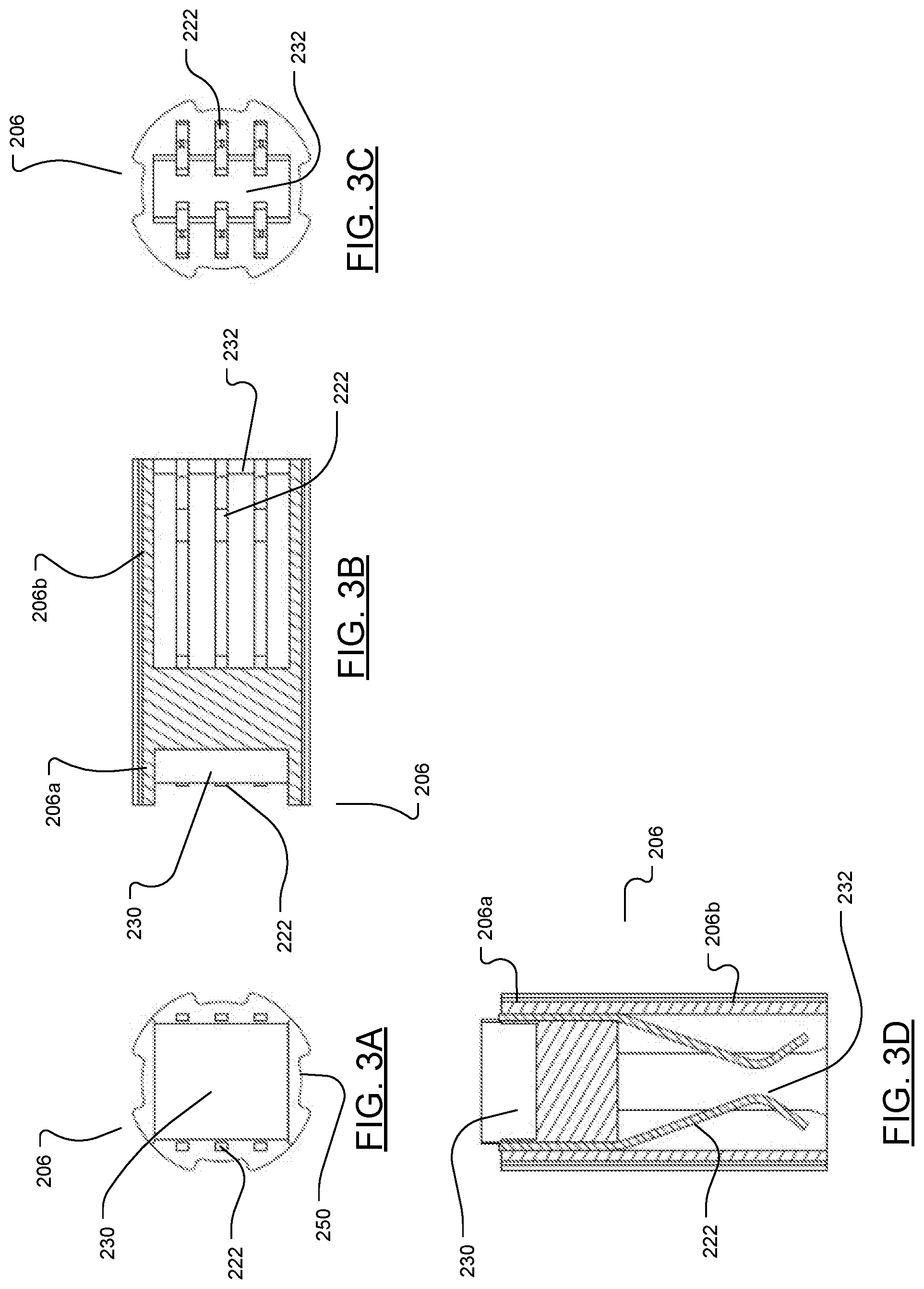
Referring now to FIGS. 3A-3D, the figures illustrate a front, side cross-sectional, rear, and bottom cross-sectional views, respectively, of the card edge connector device 206 in accordance with the principles and teachings of the disclosure. The card edge connector 206 of FIGS. 3A-3D is illustrated without the scope or endoscopic device, including the outer scope tube 202, for purposes of clarity and simplicity in discussing the details of the connector 206.
It will be appreciated that the card edge connector 206 may be configured, dimensioned and built to help minimize the overall size of the package, for example, in the x-dimension (width) and the y-dimension (height). Accordingly, one end 206a of the connector 206, which may be a first end or at the distal end or distal portion, may be optimized for placement of the sensor 208 in order to protect the wire-bonds that may connect the sensor 208 to the plurality of electrical connectors 222, such as pins or pads, of the connector 206, and to provide overall protection of the sensor 208.
To facilitate the above, the card edge connector 206 may comprise a cavity or recess 230 for receiving therein the sensor 208 and silicon die. The other end 206b, which may be a second end or a proximal end, of the connector 206 may be optimized to accept the edge card PCBA 210 (illustrated best in FIGS. 2B and 2D). At this end 206b, a first slot, socket or receptacle 232 (as illustrated best in FIGS. 3B-3D) may be provided to accept or receive therein the edge card PCBA 210. It will be appreciated that the PCBA 210 may be held in the first slot, socket or receptacle 232 via a bias force. The plurality of electrical connectors 222 may extend into the first slot, socket or receptacle 232, such that when the PCBA 210 is located within the first slot 232 the electrical connectors 222 of the connector assembly 206 may be in electrical communication with corresponding electrical connectors on the PCBA 210. The connector 206 may further comprise a vertical slot or channel 250 for receiving fiber optic cable strands therein.
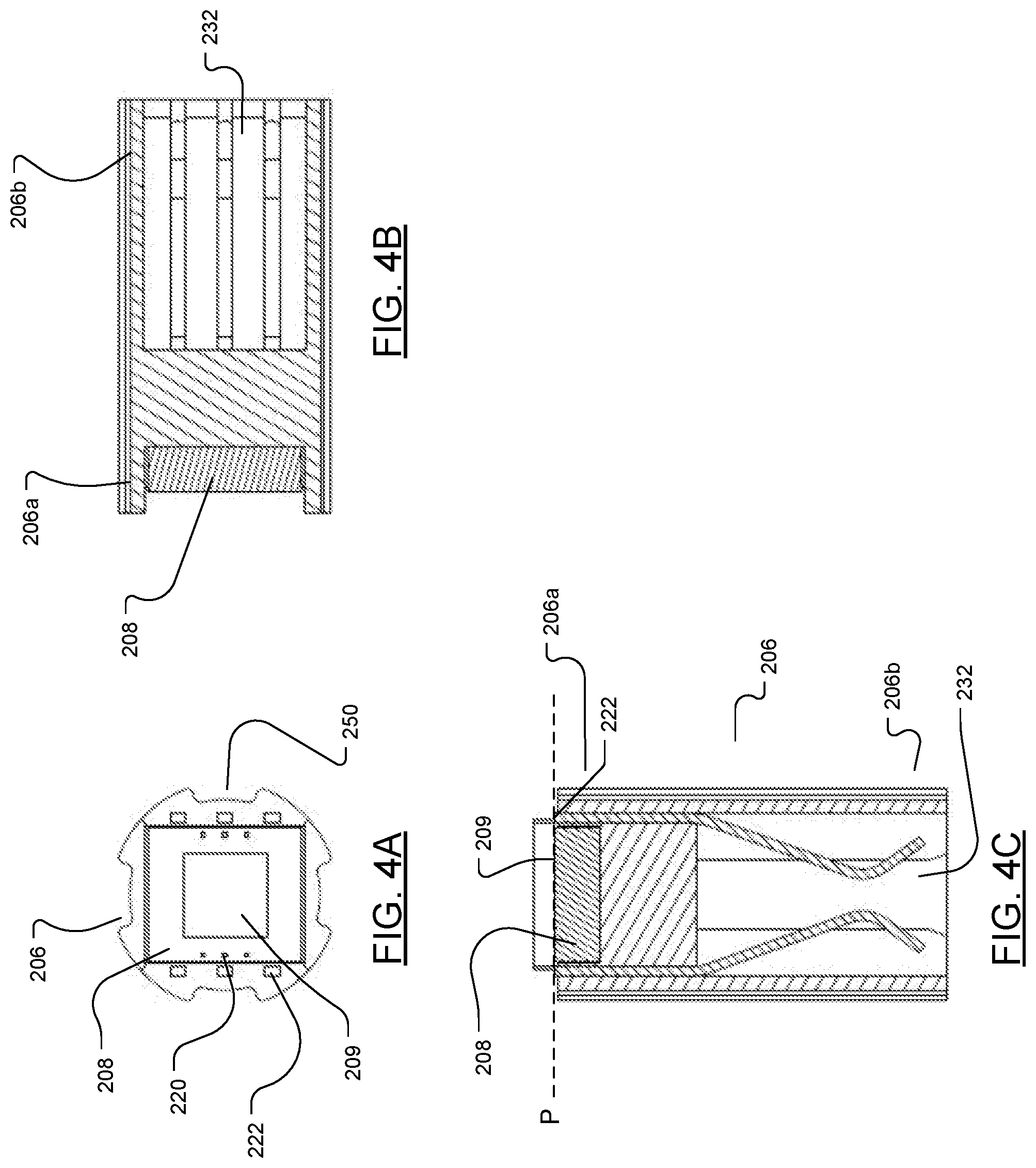
FIGS. 4A-4C illustrate a front, side cross-sectional, and bottom cross-sectional views, respectively, of the card edge connector device 206 with a sensor 208 loaded therein in accordance with the principles and teachings of the disclosure. It will be appreciated that the sensor 208 may be loaded in the cavity 230 as discussed above in connection with FIGS. 3A-3D. It will be appreciated that the imaging sensor 208 and silicon die may be attached or otherwise connected to the connector 206 using any mechanical mechanism and/or an adhesive or other bond. For example, the imaging sensor 208 may comprise a plurality of sensor pads or electrical connectors 220 that may be bonded or otherwise connected to the electrical connectors 222 of the card edge connector 206 with a plurality of bonds 221, such as wire bonds.
In the configuration illustrated in FIGS. 4A-4C, the pixel array 209 of the image sensor 208 is located on the same plane or substantially the same plane (illustrated by dashed line P in FIG. 4C) as the electrical connectors 222 at the first end 206a of the connector assembly 206.
In an implementation of the disclosure illustrated best in FIGS. 7A-7C, adhesive may be used to attach the sensor 208 to the connector 206. The adhesive may be electrically conductive adhesive, and may be, for example, gold or silver filled adhesive or other metallic filled adhesive. The adhesive may be placed in controlled locations of the connector 206 to electrically connect the silicon die to a specific pin of the connector 206, such as the ground pin. As illustrated best in FIG. 7C, the controlled location may be an individual cavity or other receptacle 224 to receive the electrically conductive adhesive therein. As illustrated in 7C, a ground pin 222a is shown as being electrically connected to the sensor pad 220 by a wire bond 221 to the ground pin 222a. In other words, the ground pin 222a may be electrically connected to the silicon die of the sensor by an electrically conductive adhesive to provide an improved electrical ground path for the sensor. As illustrated, the wire bond 221 may be run on the outside of the sensor to the one or more electrical connectors 222, such as pins. It will be appreciated that the attachment of the electrically conductive adhesive to the ground pin 222a may reduce the amount of noise in the sensor 208 and may increase signal integrity as compared to a sensor attached to a ground pin without any epoxy or electrically conductive adhesive.
FIGS. 5A-5C illustrate front, side cross-sectional, and bottom cross-sectional views, respectively, of the card edge connector device 206 with a sensor 208 loaded therein with wire bonds 221 connecting the sensor 208 to electrical connectors 222, such as pins or pads, of the connector 206 in accordance with the principles and teachings of the disclosure. As illustrated best in FIG. 5B, the connector 206 may comprise the cavity 230 that may be defined by a sidewall 209. In various implementations, the sidewall 209 may comprise a height, such that the sidewall 209 extends above and beyond the sensor 208. In various implementations, the connector assembly 206 may comprise the cavity 230 or a partial cavity that may comprise a sidewall 209 and that is located at the first end 206a of the connector 206. It will be appreciated that the image sensor 208 may be located within the cavity 230 or partial cavity, such that the sidewall 209 surrounds at least a portion of the image sensor 208, thereby protecting the image sensor 208 and electrical connectors 221, 222 from damage. In an implementation, the image sensor 208 may be completely surrounded by the sidewall 209. In an implementation, the image sensor 208 may be partially surrounded by the sidewall 209. In an implementation, the image sensor 208 may not be surrounded by the sidewall 209, but may instead sit proud of and with respect to the connector 206.
In the configuration illustrated in FIGS. 5A-5C, the pixel array 209 of the image sensor 208 is located on the same plane or substantially the same plane (illustrated by dashed line P in FIG. 5C) as the electrical connectors 222 at the first end 206a of the connector assembly 206.
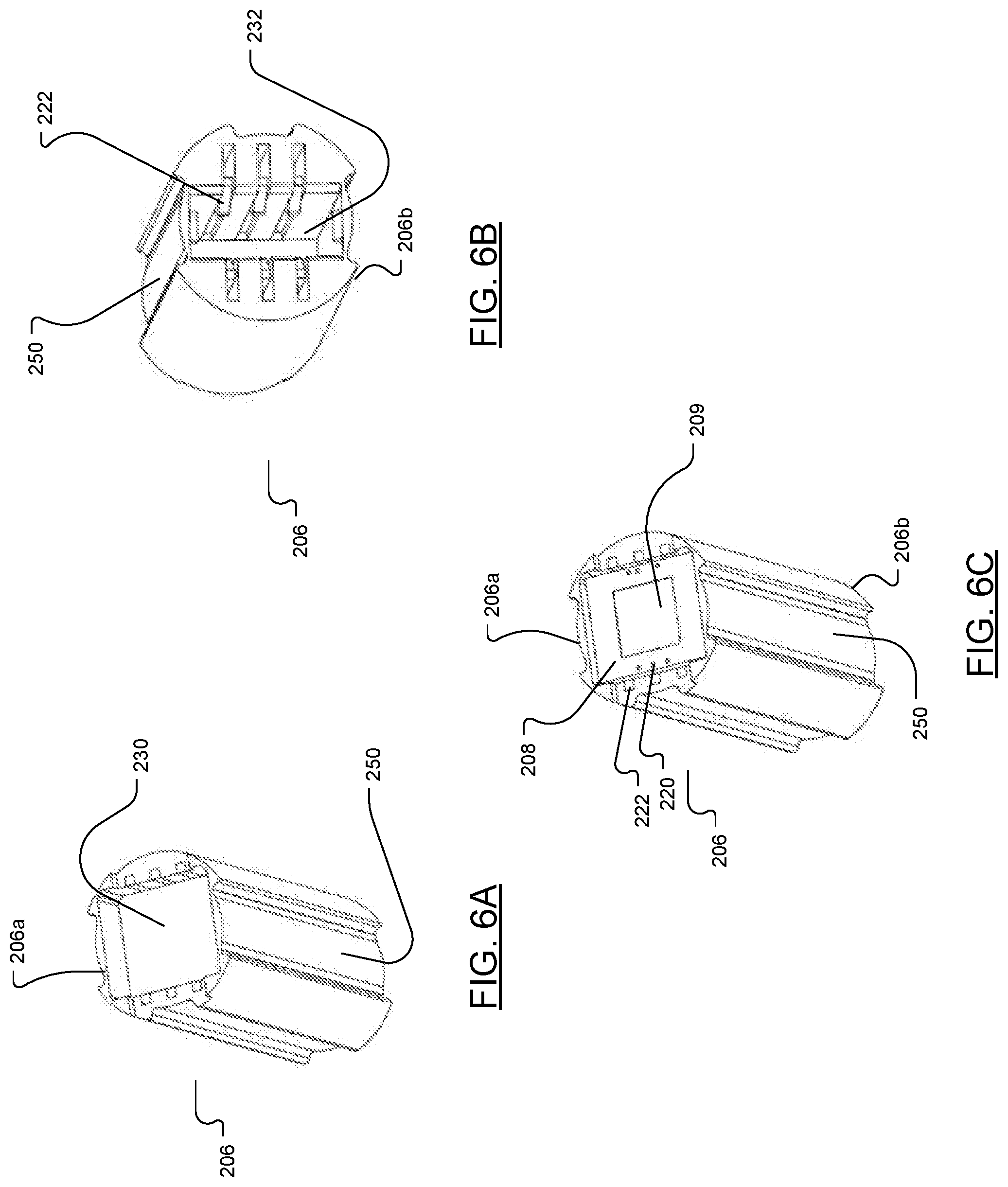
FIGS. 6A-6C illustrate a front, three-dimensional view of the card edge connector device 206, a rear, three-dimensional view of the card edge connector device 206, and a front, three-dimensional view of the card edge connector device 206 with a sensor 208 loaded therein, respectively, in accordance with the principles and teachings of the disclosure. The three images illustrated in FIGS. 6A-6C, illustrate the concept disclosed herein for the card edge connector 206. In an implementation, the housing of the connector 206 may comprise 3.5 mm housing outer diameter. In an implementation, the connector 206 may comprise six contacts or electrical connectors 222. In an implementation, the connector 206 may comprise a fine pitch (e.g., about 0.5 mm to about 0.6 mm) In an implementation, the connector 206 may comprise a first end or distal end 206a comprising the cavity or recess 230 to hold and receive the sensor die therein. In an implementation, the connector 206 may comprise a second end or proximal end 206b comprising a socket or receptacle 232 to accept or receive a micro edge card or PCBA therein. In an implementation, the PCBA may comprise a rigid PCB and features to connect a wire harness as is known in the art. In an implementation, the PCBA may comprise a flat flexible PCB.
FIGS. 7A-7C illustrate front, side cross-sectional and bottom cross-sectional views, respectively, of a card edge connector device 206 with a sensor 208 loaded proud of a plane of the connector in accordance with the principles and teachings of the disclosure. The figures illustrate an implementation in which the sensor 208 may sit proud above the plane (represented by dashed line P) of the electrical connectors 222, such as pins or pads, at the first end 206a of the connector assembly 206 as illustrated best in FIG. 7C. In this configuration, the pixel array 209 of the image sensor 208 is located above a plane (represented by dashed line P) of the electrical connectors 222 at the first end 206a of the connector assembly 206. This configuration may allow the electrical connectors 222, such as pins or pads, of the connector assembly 206 to sit under the sensor 208 rather than being positioned on either side of the sensor 208 as in other implementations disclosed herein. This configuration may enable a smaller overall housing diameter and an overall smaller housing package or assembly for use with tubular members having small diameters, such as an endoscope having a diameter of 5 mm or less.
In an implementation of the disclosure illustrated best in FIGS. 7A-7C, adhesive may be placed in controlled locations of the connector 206 to electrically connect the silicon die of the image sensor 208 to a specific pin of the connector 206, such as the ground pin. As illustrated best in FIG. 7C, the controlled location may be an individual cavity or other receptacle 224 to receive the electrically conductive adhesive therein. As illustrated in 7C, a ground pin 222a is shown as being electrically connected to the sensor pad 220 by a wire bond 221 to the ground pin 222a. In other words, the ground pin 222a may be electrically connected to the silicon die of the sensor by an electrically conductive adhesive to provide an improved electrical ground path for the sensor. As illustrated, the wire bond 221 may be run on the outside of the sensor to the one or more electrical connectors 222, such as pins. This configuration allows for an overall smaller housing for use with tubular members having small diameters, such as an endoscope having a diameter of 5 mm or less. It will be appreciated that the attachment of the electrically conductive adhesive to the ground pin 222a may reduce the amount of noise in the sensor 208 and may increase signal integrity as compared to a sensor attached to a ground pin without any epoxy or electrically conductive adhesive.
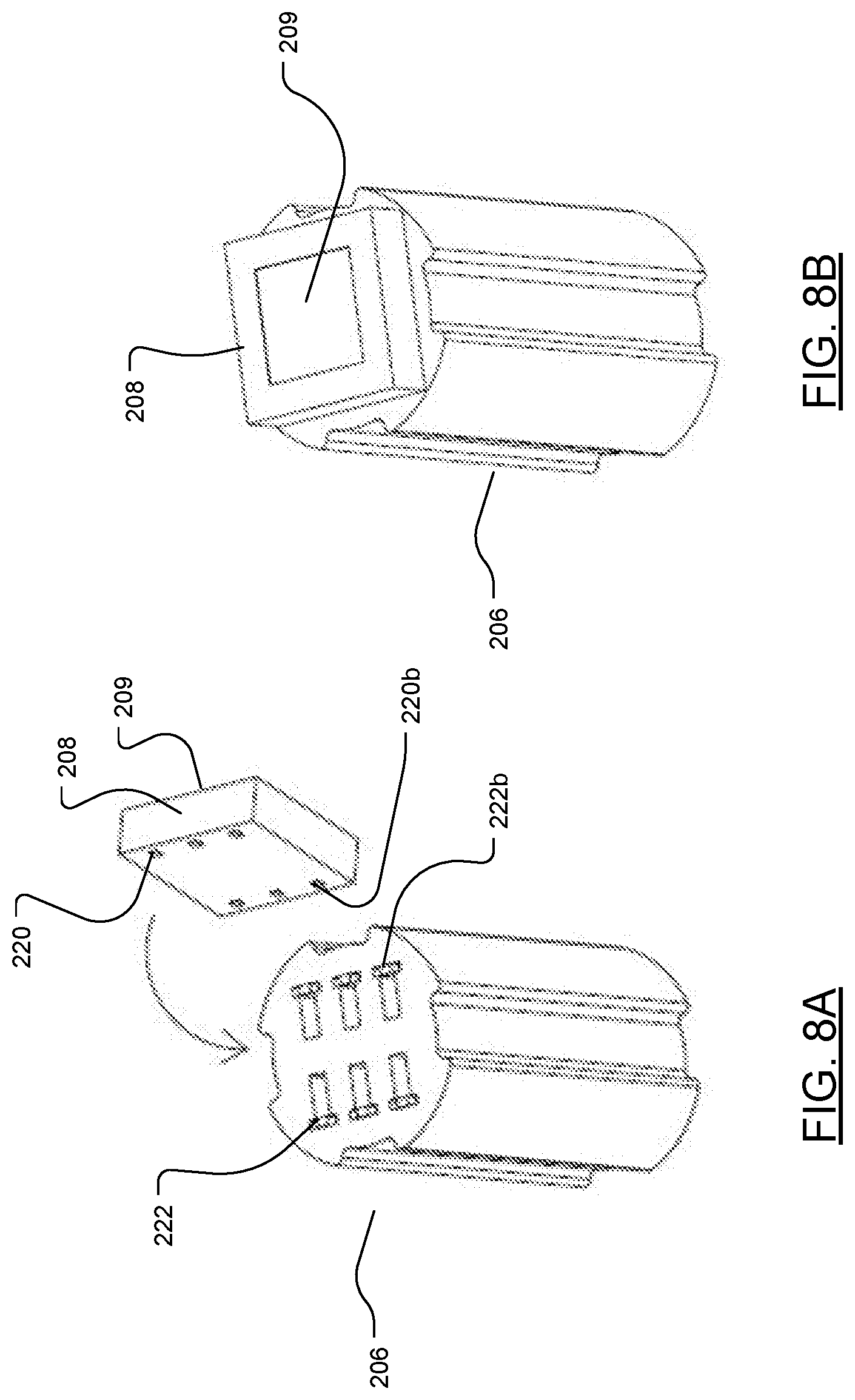
FIGS. 8A-8B illustrate perspective views of a card edge connector device 206 for use with a backside illuminated sensor 208 loaded proud of a plane P of the connector 206 in accordance with the principles and teachings of the disclosure. In this implementation, the pixel array 209 of the image sensor 208 is located above a plane of the electrical connectors 222 at the first end 206a of the connector assembly 206. The figures illustrate an implementation in which the sensor 208 is constructed using a backside illumination (BSI) manufacturing process resulting in the sensor pads 220 being located on the opposite side of the silicon die as the pixel array 209. As shown, this BSI sensor may be used with the card edge connector 206 disclosed herein. The pads 220 of BSI sensor 208 may be bonded directly to the electrical connectors 222, such as pins or pads, of the card edge connector 206 without the need for wire bonds. Referring specifically to FIG. 8A, pad 220b may be bonded directly to the electrical connector 222b without the need for wire bonds. Such direct bonding may occur with respect to all sensor pads 220 and all electrical connectors 222. It will be appreciated that the pads 220 that may be located on the underside of the sensor 208 may be soldered onto the electrical connectors 222 of the connector assembly 206.
FIGS. 9A-9C illustrate front, side cross-sectional and bottom cross-sectional views, respectively, of a card edge connector device 206 with a sensor 208 loaded proud of a plane (represented by dashed line P) at the first end 206a of the connector assembly 206 in accordance with the principles and teachings of the disclosure. In this implementation, the pixel array 209 of the image sensor 208 is located above a plane (represented by dashed line P) of the electrical connectors 222 at the first end 206a of the connector assembly 206.
The figures illustrate an implementation in which the sensor 208 is constructed using a backside illumination (BSI) manufacturing process resulting in the sensor pads 220 being located on the opposite side of the silicon die as the pixel array 209. As can be seen in FIGS. 9A-9C, which implement the details of FIGS. 8A-8B, this configuration may allow the card edge connector 206 diameter to shrink with respect to the size of the sensor 208 resulting in a more efficient use of the limited space available in a tubular member having a sensor located distally therein, while still retaining the benefits of the connector assembly 206. This efficiency gain can be used to put a larger sensor in a specific scope diameter, or to shrink the scope diameter around a specific sensor size, either of which may result in improved clinical efficiency.
It will be appreciated that the disclosure illustrates in FIGS. 1A-6C and describes herein novel devices, systems and methods for packaging a silicon imaging sensor die that: (1) protects the sensor 208 and wire bonds 221 from damage; and/or (2) minimizes the footprint of the final card edge connector 206 assembly; and/or (3) enables simple mechanical connection to a PCBA with an attached wire harness that carries data to a remote or off-site image processing hardware. The above characteristics may be important for applications in which space is minimal, such as in an endoscopic application with the image sensor located distally within a tip of the scope or any other application in which physical space is limited.
FIGS. 10A and 10B illustrate a top view and a cross-sectional view, respectively, of a conventional, prior art packaged imaging sensor device. It will be appreciated that the connector 206 of the disclosure provides significant advantages over a conventional package for an image sensor. A common method of packaging silicon die comprising an imaging sensor is illustrated. It will be appreciated that the ceramic package has a glass lid to protect the die and the wire bonds as illustrated. Conventional packages are optimized to keep height of the image sensor to a minimum, but the footprint of the image sensor is very large in comparison to the footprint of the image sensor disclosed herein. Due to the mechanical constraints of being located within a tip or distal end of an endoscope or other application where space is constrained, a large footprint is unworkable or undesirable. Conventional packages for an image sensor are optimized for a surface-mount solder process to attach the PCBA, which has local image processing hardware and circuitry (e.g., image processing hardware and circuitry on the same PCBA as the image sensor), but such a configuration may be difficult to connect to a wire harness.
It will be appreciated that the teachings and principles of the disclosure may be used in a reusable device platform, a limited use device platform, a re-posable use device platform, or a single-use/disposable device platform without departing from the scope of the disclosure. It will be appreciated that in a re-usable device platform an end-user is responsible for cleaning and sterilization of the device. In a limited use device platform the device can be used for some specified amount of times before becoming inoperable. Typical new device is delivered sterile with additional uses requiring the end-user to clean and sterilize before additional uses. In a re-posable use device platform a third-party may reprocess the device (e.g., cleans, packages and sterilizes) a single-use device for additional uses at a lower cost than a new unit. In a single-use/disposable device platform a device is provided sterile to the operating room and used only once before being disposed of.
In the foregoing Detailed Description of the Disclosure, various features of the disclosure may have been grouped together in a single embodiment for the purpose of streamlining the disclosure. This method of disclosure is not to be interpreted as reflecting an intention that the claimed disclosure requires more features than are expressly recited in each claim. Rather, inventive aspects lie in less than all features of a single foregoing disclosed embodiment.
It is to be understood that the above-described arrangements are only illustrative of the application of the principles of the disclosure. Numerous modifications and alternative arrangements may be devised by those skilled in the art without departing from the spirit and scope of the disclosure and the appended claims are intended to cover such modifications and arrangements.
Thus, while the disclosure has been shown in the drawings and described above with particularity and detail, it will be apparent to those of ordinary skill in the art that numerous modifications, including, but not limited to, variations in size, materials, shape, form, function and manner of operation, assembly and use may be made without departing from the principles and concepts set forth herein.
Further, where appropriate, functions described herein can be performed in one or more of: hardware, software, firmware, digital components, or analog components. For example, one or more application specific integrated circuits (ASICs) can be programmed to carry out one or more of the systems and procedures described herein. Certain terms are used throughout the following description and Claims to refer to particular system components. As one skilled in the art will appreciate, components may be referred to by different names. This document does not intend to distinguish between components that differ in name, but not function.
* * * * *
References
D00000
D00001
D00002
D00003
D00004
D00005
D00006
D00007
D00008
D00009
D00010
XML
uspto.report is an independent third-party trademark research tool that is not affiliated, endorsed, or sponsored by the United States Patent and Trademark Office (USPTO) or any other governmental organization. The information provided by uspto.report is based on publicly available data at the time of writing and is intended for informational purposes only.
While we strive to provide accurate and up-to-date information, we do not guarantee the accuracy, completeness, reliability, or suitability of the information displayed on this site. The use of this site is at your own risk. Any reliance you place on such information is therefore strictly at your own risk.
All official trademark data, including owner information, should be verified by visiting the official USPTO website at www.uspto.gov. This site is not intended to replace professional legal advice and should not be used as a substitute for consulting with a legal professional who is knowledgeable about trademark law.