Method for precisely aligning backside pattern to frontside pattern of a semiconductor wafer
Zhang , et al. November 10, 2
U.S. patent number 10,833,021 [Application Number 16/009,144] was granted by the patent office on 2020-11-10 for method for precisely aligning backside pattern to frontside pattern of a semiconductor wafer. This patent grant is currently assigned to ALPHA AND OMEGA SEMICONDUCTOR (CAYMAN) LTD.. The grantee listed for this patent is Alpha and Omega Semiconductor (Cayman) Ltd.. Invention is credited to Runtao Ning, Jian Wang, Hongyong Xue, Lei Zhang.


| United States Patent | 10,833,021 |
| Zhang , et al. | November 10, 2020 |
Method for precisely aligning backside pattern to frontside pattern of a semiconductor wafer
Abstract
A method comprises the steps of providing a semiconductor device wafer; forming a first plurality of alignment marks on a first side of the semiconductor device wafer; forming a first pattern of a first conductivity type; forming a second plurality of alignment marks on a second side of the semiconductor device wafer; forming a bonded wafer by bonding a carrier wafer to the semiconductor device wafer; forming a third plurality of alignment marks on a free side of the carrier wafer; applying a grinding process; forming a plurality of device structure members; removing the carrier wafer; applying an implanting process and an annealing process; applying a metallization process and applying a singulation process.
| Inventors: | Zhang; Lei (Portland, OR), Xue; Hongyong (Portland, OR), Wang; Jian (Portland, OR), Ning; Runtao (Hillsboro, CA) | ||||||||||
|---|---|---|---|---|---|---|---|---|---|---|---|
| Applicant: |
|
||||||||||
| Assignee: | ALPHA AND OMEGA SEMICONDUCTOR
(CAYMAN) LTD. (Grand Cayman, KY) |
||||||||||
| Family ID: | 1000005175181 | ||||||||||
| Appl. No.: | 16/009,144 | ||||||||||
| Filed: | June 14, 2018 |
Prior Publication Data
| Document Identifier | Publication Date | |
|---|---|---|
| US 20190006285 A1 | Jan 3, 2019 | |
Related U.S. Patent Documents
| Application Number | Filing Date | Patent Number | Issue Date | ||
|---|---|---|---|---|---|
| 15637361 | Jun 29, 2017 | 10170559 | |||
| 15637352 | Jun 29, 2017 | ||||
| Current U.S. Class: | 1/1 |
| Current CPC Class: | H01L 21/67282 (20130101); H01L 23/544 (20130101); H01L 21/6835 (20130101); H01L 21/78 (20130101); H01L 2221/6835 (20130101); H01L 2221/68381 (20130101); H01L 2221/68327 (20130101); H01L 21/265 (20130101); H01L 2221/68309 (20130101); H01L 2223/54426 (20130101); H01L 29/66325 (20130101); H01L 21/304 (20130101); H01L 2223/54453 (20130101) |
| Current International Class: | H01L 23/544 (20060101); H01L 21/67 (20060101); H01L 21/304 (20060101); H01L 21/265 (20060101); H01L 21/78 (20060101); H01L 29/66 (20060101); H01L 21/683 (20060101) |
| Field of Search: | ;438/401,455,459 |
References Cited [Referenced By]
U.S. Patent Documents
| 5414290 | May 1995 | Bauer |
| 5952694 | September 1999 | Miyawaki |
| 7538412 | May 2009 | Schulze et al. |
| 7910486 | March 2011 | Yilmaz et al. |
| 8003502 | August 2011 | Mauder et al. |
| 8084814 | December 2011 | Nemoto et al. |
| 8148749 | April 2012 | Grebs et al. |
| 8299494 | October 2012 | Yilmaz et al. |
| 8653556 | February 2014 | Niedernostheide et al. |
| 9129851 | September 2015 | Kouno et al. |
| 9825023 | November 2017 | Basler et al. |
| 2013/0149836 | June 2013 | Wang |
| 2013/0328105 | December 2013 | Matsuura |
| 2014/0027814 | January 2014 | Pfirsch |
| 2015/0214055 | July 2015 | Blanchard |
| 2015/0228723 | August 2015 | Werber et al. |
| 2015/0236142 | August 2015 | Laven et al. |
| 2015/0325440 | November 2015 | Schulze et al. |
| 2016/0093690 | March 2016 | Falck et al. |
| 2016/0111415 | April 2016 | Basler et al. |
| 2016/0197143 | July 2016 | Naito |
| 2016/0211257 | July 2016 | Yoshida |
| 2016/0284803 | September 2016 | Baburske et al. |
| 2016/0322472 | November 2016 | Schloegl et al. |
Other References
|
FG.C. Bijnen, W.V. Buel, M. Young, X. Zhou, C. Gooch, Back-side alignment strategy decouples process from alignment and achieves leading edge overlay performance, Microelectronic Engineering, vol. 83, Issues 4-9, 2006, pp. 647-650, ISSN 0167-9317 (Year: 2006). cited by examiner . Matthias et al. 1.7kV High-Power IGBT Fabrication by Bonded-Water-Concept. Proceedings of the 27th International Symposium on Power Semiconductor Devices & IC's May 10-14, 2015, Kowloon Shangri-La , Hongkong. cited by applicant. |
Primary Examiner: Shamsuzzaman; Mohammed
Assistant Examiner: Gray; Aaron J
Attorney, Agent or Firm: Lin; Chen-Chi
Parent Case Text
CROSS-REFERENCE TO RELATED APPLICATIONS
This Patent Application is a Continuation in Part (CIP) Application of a pending application Ser. No. 15/637,352 filed on Jun. 29, 2017 by having a common inventor. This Patent Application is a Continuation in Part (CIP) Application of a pending application Ser. No. 15/637,361 filed on Jun. 29, 2017 by having a common inventor. The Disclosure made in the patent application Ser. No. 15/637,352 and patent application Ser. No. 15/637,361 are hereby incorporated by reference.
Claims
The invention claimed is:
1. A method for fabricating semiconductor devices, the method comprising the steps of: providing a semiconductor device water comprising a first side and a second side opposite the first side; forming a first plurality of alignment marks on the first side of the semiconductor device wafer; forming a first pattern of a first conductivity type on the first side of the semiconductor device wafer by referencing the first plurality of alignment marks; forming a second plurality of alignment marks on the second side of the semiconductor device wafer by referencing the first plurality of alignment marks; forming a bonded wafer by bonding a carrier wafer to the first side of the semiconductor device wafer, the carrier wafer comprising a bonded side and a free side; forming a third plurality of alignment marks on the free side of the carrier wafer by referencing the second plurality of alignment marks; applying a grinding process to the second side of the semiconductor device wafer of the bonded wafer reducing a thickness of the semiconductor device wafer and exposing a grinded surface; forming a plurality of device structure members on the grinded surface forming a bonded processed wafer; removing the carrier wafer from the bonded processed wafer forming a processed wafer; applying an implanting process and an annealing process forming a plurality of regions of a second conductivity type on the first side of the semiconductor device wafer adjacent to the first pattern of the first conductivity type; and applying a metallization process forming a product wafer; wherein the step of forming the first pattern oi the first conductivity type is before the step of forming the bonded wafer; wherein the step of forming the second plurality of alignment marks is before the step of forming the bonded wafer; wherein the step of forming the bonded wafer is before the step of forming the third plurality of alignment marks; and wherein the step of forming the bonded wafer is before the step of applying the implanting process and the annealing process forming the plurality of regions of the second conductivity type.
2. The method for fabricating semiconductor devices of claim 1, after the step of applying the metallization process, applying a singulation process to the product wafer forming a plurality of separated semiconductor devices.
3. The method for fabricating semiconductor devices of claim 2, wherein the plurality of separated semiconductor devices are a plurality of reverse conducting insulated-gate bipolar transistors.
4. The method for fabricating semiconductor devices of claim 1, wherein the carrier wafer comprises a silicon substrate and a silicon oxide layer; wherein the silicon oxide layer is located at the bonded side of the carrier wafer; and wherein the step of forming the bonded wafer by bonding the carrier wafer to the first side of the semiconductor device wafer comprises forming the bonded wafer by bonding the silicon oxide layer of the carrier wafer to the first side of the semiconductor device wafer.
5. The method for fabricating semiconductor devices of claim 4, wherein the step of removing the carrier wafer from the bonded processed wafer comprises the sub-steps of grinding off the silicon substrate of the carrier wafer; and stripping off the silicon oxide layer of the carrier wafer.
6. The method for fabricating semiconductor devices of claim 1, wherein the semiconductor device wafer comprises a silicon oxide layer located at the first side of the semiconductor device wafer; wherein the carrier wafer comprises a silicon substrate and a silicon oxide layer; wherein the silicon oxide layer is located at the bonded side of the carrier wafer; and wherein the step of forming the bonded wafer by bonding the carrier wafer to the first side of the semiconductor device wafer comprises forming the bonded wafer by bonding the silicon oxide layer of the carrier wafer to the silicon oxide layer of the semiconductor device wafer.
7. The method for fabricating semiconductor devices of claim 6, wherein the step of removing the carrier wafer from the bonded processed wafer comprises the sub-steps of grinding off the silicon substrate of the carrier wafer; and stripping off the silicon oxide layer of the carrier wafer; and wherein the method for fabricating semiconductor devices further comprises, after the step of removing the carrier wafer from the bonded processed wafer, stripping off the silicon oxide layer of the semiconductor device wafer.
8. The method for fabricating semiconductor devices of claim 1, wherein the step of forming the plurality of device structure members on the grinded surface comprises the sub-steps of forming a first plurality of regions of the second conductivity type; forming a second plurality of regions of the first conductivity type; forming a plurality of source regions; and forming a plurality of gate regions.
9. The method for fabricating semiconductor devices of claim 1, before the step of forming the plurality of device structure members on the grinded surface, forming a fourth plurality of alignment marks on the grinded surface referencing the third plurality of alignment marks.
10. The method for fabricating semiconductor devices of claim 9, wherein the step of forming the plurality of device structure members on the grinded surface comprises the sub-steps of forming a first plurality of regions of the second conductivity type referencing the fourth plurality of alignment marks; forming a second plurality of regions of the first conductivity type referencing the fourth plurality of alignment marks; forming a plurality of source regions referencing the fourth plurality of alignment marks; and forming a plurality of gate regions referencing the fourth plurality of alignment marks.
11. The method for fabricating semiconductor devices of claim 1, wherein the semiconductor device wafer is a monocrystalline Czochralski silicon wafer.
12. The method for fabricating semiconductor devices of claim 1, wherein the semiconductor device wafer is a magnetic field applied Czochralski silicon wafer.
13. The method for fabricating semiconductor devices of claim 1, wherein the semiconductor device wafer is a floating zone silicon wafer.
14. The method for fabricating semiconductor devices of claim 1, an ASML 3DALIGN machine is used to conduct the step of forming the second plurality of alignment marks on the second side of the semiconductor device wafer by referencing the first plurality of alignment marks.
Description
FIELD OF THE INVENTION
This invention relates generally to a method of fabricating semiconductor devices by precisely aligning backside pattern to frontside pattern of a semiconductor wafer. More particularly, the present invention relates the method referencing three or more sets of alignment marks.
BACKGROUND OF THE INVENTION
Fabrication of a reverse conducting insulated-gate bipolar transistor (RC-IGBT) requires N and P alternating patterns on a backside of a silicon wafer. The backside pattern is not precisely aligned with a frontside pattern because the silicon wafer faces down (the frontside pattern is not accessible) during a backside patterning process. A conventional fabrication method using a notch on the silicon wafer introduces large alignment errors (in the order of 20 microns) between the backside pattern and the frontside pattern.
The present disclosure references three or more sets of alignment marks. The alignment accuracy is improved and can be as good as a solely frontside process only. For example, the misalignment is less than 120 nanometers by using an i-line stepper and the misalignment is less than 60 nanometers by using a DUV stepper.
Because of the improved alignment, the present disclosure can be applied to fabrication of semiconductor devices having complicated device structure members requiring tight tolerances. The present disclosure can also be applied to a metal pattern etching process at the backside requiring precise alignment to the frontside.
SUMMARY OF THE INVENTION
The present invention discloses a method for fabricating semiconductor devices. The method comprises the steps of providing a semiconductor device wafer; forming a first plurality of alignment marks on a first side of the semiconductor device wafer; forming a first pattern of a first conductivity type; forming a second plurality of alignment marks on a second side of the semiconductor device wafer; forming a bonded wafer by bonding a carrier wafer to the semiconductor device wafer; forming a third plurality of alignment marks on a free side of the carrier wafer; applying a grinding process; forming a plurality of device structure members; removing the carrier wafer; applying an implanting process and an annealing process; applying a metallization process and applying a singulation process.
The step of bonding the carrier wafer to the semiconductor device wafer facilitates handling of the thinned semiconductor device wafer.
BRIEF DESCRIPTION OF THE DRAWINGS
FIG. 1 is a flowchart of a process to fabricate a semiconductor device in examples of the present disclosure.
FIGS. 2A, 2B, 2C, 2D, 2E, 2F, 2G, 2H, 2I, 2J, 2K, 2L, 2M, 2N and 2O show cross sectional views of steps of the process to fabricate the semiconductor device of FIG. 1 in examples of the present disclosure.
FIGS. 3A and 3B are exploded, cross sectional views of two bonded wafers respectively in examples of the present disclosure.
DETAILED DESCRIPTION OF THE INVENTION
FIG. 1 is a flowchart of a process 100 to fabricate a semiconductor device in examples of the present disclosure. The process 100 may begin in block 102.
In block 102, a semiconductor device wafer 210 of FIG. 2A is provided. In one example, the semiconductor device wafer 210 is a silicon wafer of 8-inch diameter and 725 .mu.m thickness. In another example, the semiconductor device wafer 210 is a silicon wafer of 12-inch diameter and 775 .mu.m thickness. In examples of the present disclosure, the semiconductor device wafer 210 is a monocrystalline Czochralski silicon (Cz) wafer, a magnetic field applied Cz (MCZ) wafer, a floating zone silicon (FZ) wafer, or an epitaxial (EPI) wafer. The semiconductor device wafer 210 has a first side 202 (for example, frontside) and a second side 204 (for example, backside). The second side 204 opposites the first side 202. Block 102 may be followed by block 104.
In block 104, a first plurality of alignment marks 212 of FIG. 2A are formed on the first side 202 of the semiconductor device wafer 210. Block 104 may be followed by block 106.
In block 106, a first pattern 214 of FIG. 2B of a first conductivity type (for example, N+) is formed on the first side 202 of the semiconductor device wafer 210 by referencing the first plurality of alignment marks 212. Block 106 may be followed by block 108.
In block 108, the semiconductor device wafer 210 of FIG. 2C is flipped. Block 108 may be followed by block 110.
In block 110, a second plurality of alignment marks 222 of FIG. 2C are formed on the second side 204 of the semiconductor device wafer 210 by referencing the first plurality of alignment marks 212.
In examples of the present disclosure, ASML 3DALIGN.TM. product for three dimensional alignment is used to align the second plurality of alignment marks 222 of FIG. 2C to the first plurality of alignment marks 212. Block 110 may be followed by block 112.
In block 112, the semiconductor device wafer 210 of FIG. 2D is flipped. Block 112 may be followed by block 114.
In block 114, a bonded wafer 208 of FIG. 2E is formed by bonding a carrier wafer 229 to the first side 202 of the semiconductor device wafer 210. The carrier wafer 229 has a bonded side 231 and a free side 233.
In one example, the carrier wafer 229 has a silicon substrate 230 of FIG. 3A and a silicon oxide layer 336 of FIG. 3A. The silicon oxide layer 336 is located at the bonded side 231 of the carrier wafer 229. The bonded wafer 208 is formed by bonding the silicon oxide layer 336 of the carrier wafer 229 to the first side 202 of the semiconductor device wafer 210 (in one example, made of silicon). The silicon oxide layer 236 of FIG. 2E contains solely the silicon oxide layer 336 of FIG. 3A.
In another example, a silicon oxide layer 314 of FIG. 3B is grown and is directly attached to the first side 202 of the semiconductor device wafer 210. The carrier wafer 229 has a silicon substrate 230 of FIG. 3B and a silicon oxide layer 334 of FIG. 3B. The silicon oxide layer 334 is located at the bonded side 231 of the carrier wafer 229. The bonded wafer 208 is formed by bonding the silicon oxide layer 334 of the carrier wafer 229 to silicon oxide layer 314. The silicon oxide layer 236 of FIG. 2E contains the silicon oxide layer 314 and the silicon oxide layer 334 of FIG. 3B. Block 114 may be followed by block 116.
In block 116, a third plurality of alignment marks 242 of FIG. 2F are formed on the free side 233 of the carrier wafer 229 by referencing the second plurality of alignment marks 222. Block 116 may be followed by block 118.
In block 118, the bonded wafer 208 of FIG. 2G is flipped. Block 118 may be followed by block 120.
In block 120, a grinding process is applied to the second side 204 of FIG. 2G of the semiconductor device wafer of the bonded wafer 208. A thickness 254 of FIG. 2H of the semiconductor device wafer is reduced. A grinded surface 258 of FIG. 2H is exposed. Block 120 may be followed by block 122.
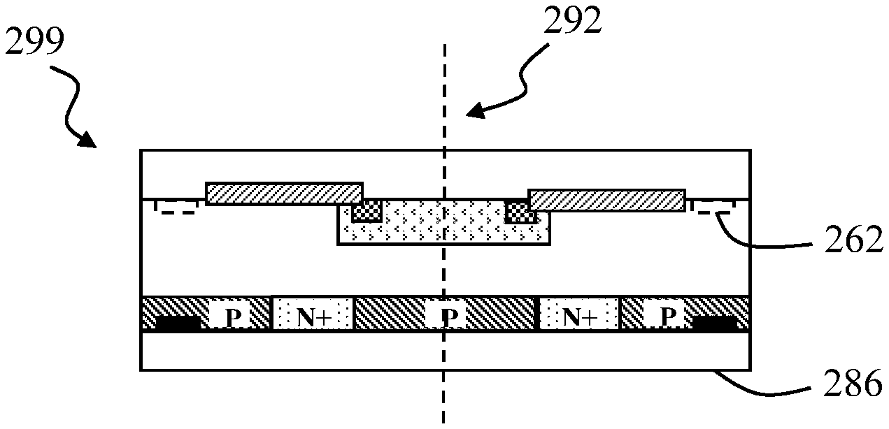
FIG. 2I shows an optional processing step. A (optional) fourth plurality of alignment marks 262 (shown in dashed lines) are formed on the grinded surface 258 by referencing the third plurality of alignment marks 222.
In block 122, a plurality of device structure members are formed on the grinded surface forming a bonded processed wafer 293 of FIG. 2J. The plurality of device structure members include a first plurality of regions 271 of the second conductivity type (for example, P), a second plurality of regions 273 of the first conductivity type (for example, N+), a plurality of source regions 275 and a plurality of gate regions 277.
In examples of the present disclosure, the plurality of device structure members are formed by referencing the fourth plurality of alignment marks 262. Block 122 may be followed by block 124.
In block 124, the carrier wafer is removed from the bonded processed wafer 293 of FIG. 2J forming a processed wafer 297 of FIG. 2L. In one example, the silicon substrate 230 is removed (for example, be a grinding process) followed by removing the silicon oxide layer 236 of FIG. 2K (for example, by a chemical etching process). Block 124 may be followed by block 126.
In block 126, an implanting process and an annealing process are applied so as to form a plurality of regions 284 of FIG. 2M of a second conductivity type (for example, P) adjacent to the first pattern 214 of the first conductivity type (for example, N+). In one example, no patterning process is required to form the plurality of regions 284. Block 126 may be followed by block 128.
In block 128, a metallization process is applied forming a metallization layer 286 of FIG. 2N of a product wafer 299. Block 128 may be followed by block 130.
In block 130, a singulation process 292 of FIG. 2O is applied to the product wafer 299 so as to form a plurality of separated semiconductor devices. In examples of the present disclosure, the plurality of separated semiconductor devices are a plurality of reverse conducting insulated-gate bipolar transistors (RC-IGBTs).
Those of ordinary skill in the art may recognize that modifications of the embodiments disclosed herein are possible. For example, a thickness of a carrier wafer may vary. Other modifications may occur to those of ordinary skill in this art, and all such modifications are deemed to fall within the purview of the present invention, as defined by the claims.
* * * * *
D00000
D00001
D00002
D00003
D00004
D00005
D00006
D00007
XML
uspto.report is an independent third-party trademark research tool that is not affiliated, endorsed, or sponsored by the United States Patent and Trademark Office (USPTO) or any other governmental organization. The information provided by uspto.report is based on publicly available data at the time of writing and is intended for informational purposes only.
While we strive to provide accurate and up-to-date information, we do not guarantee the accuracy, completeness, reliability, or suitability of the information displayed on this site. The use of this site is at your own risk. Any reliance you place on such information is therefore strictly at your own risk.
All official trademark data, including owner information, should be verified by visiting the official USPTO website at www.uspto.gov. This site is not intended to replace professional legal advice and should not be used as a substitute for consulting with a legal professional who is knowledgeable about trademark law.