Gas sensor packages
Kierse , et al.
U.S. patent number 10,730,743 [Application Number 16/159,477] was granted by the patent office on 2020-08-04 for gas sensor packages. This patent grant is currently assigned to Analog Devices Global Unlimited Company. The grantee listed for this patent is Analog Devices Global Unlimited Company. Invention is credited to Alfonso Berduque, Gerald Blaney, Brendan Cawley, Brian J. Coffey, Oliver J. Kierse, Donal Peter McAuliffe, Rigan McGeehan, Raymond J. Speer.


View All Diagrams
| United States Patent | 10,730,743 |
| Kierse , et al. | August 4, 2020 |
Gas sensor packages
Abstract
A gas sensor package is disclosed. The gas sensor package can include a housing defining a first chamber and a second chamber. An electrolyte can be provided in the first chamber. A gas inlet can provide fluid communication between the second chamber and the outside environs. The gas inlet can be configured to permit gas to enter the second chamber from the outside environs. An integrated device die can be mounted to the housing. The integrated device die can comprise a sensing element configured to detect the gas. The integrated device die can have a first side exposed to the first chamber and a second side exposed to the second chamber, with the first side opposite the second side.
| Inventors: | Kierse; Oliver J. (Killaloe, IE), McGeehan; Rigan (Limerick, IE), Berduque; Alfonso (Crusheen, IE), McAuliffe; Donal Peter (Raheen, IE), Speer; Raymond J. (Dalkey, IE), Cawley; Brendan (Patrickswell, IE), Coffey; Brian J. (Ennis, IE), Blaney; Gerald (Limerick, IE) | ||||||||||
|---|---|---|---|---|---|---|---|---|---|---|---|
| Applicant: |
|
||||||||||
| Assignee: | Analog Devices Global Unlimited
Company (Hamilton, BM) |
||||||||||
| Family ID: | 1000004963069 | ||||||||||
| Appl. No.: | 16/159,477 | ||||||||||
| Filed: | October 12, 2018 |
Prior Publication Data
| Document Identifier | Publication Date | |
|---|---|---|
| US 20190135614 A1 | May 9, 2019 | |
Related U.S. Patent Documents
| Application Number | Filing Date | Patent Number | Issue Date | ||
|---|---|---|---|---|---|
| 62582229 | Nov 6, 2017 | ||||
| Current U.S. Class: | 1/1 |
| Current CPC Class: | H01L 23/24 (20130101); B81B 7/0061 (20130101); H01L 23/3185 (20130101); H01L 23/49 (20130101); G01N 33/0036 (20130101); B81B 7/0051 (20130101); H01L 24/48 (20130101); G01N 27/404 (20130101); H01L 23/50 (20130101); B81C 1/00269 (20130101); H01L 23/00 (20130101); H01L 23/055 (20130101); H01L 25/0655 (20130101); H01L 23/49838 (20130101); H01L 2224/45144 (20130101); H01L 2924/181 (20130101); H01L 2224/48245 (20130101); B81B 2207/012 (20130101); H01L 2224/48091 (20130101); H01L 2224/32225 (20130101); H01L 2224/131 (20130101); H01L 2224/293 (20130101); H01L 24/29 (20130101); H01L 24/32 (20130101); H01L 2924/19105 (20130101); H01L 2224/73265 (20130101); H01L 2224/48227 (20130101); B81B 2201/0214 (20130101); H01L 2924/182 (20130101); H01L 2924/16195 (20130101); H01L 2224/26175 (20130101); H01L 2224/2929 (20130101); H01L 24/45 (20130101); H01L 2224/83138 (20130101); B81C 2203/0154 (20130101); H01L 2224/83851 (20130101); H01L 2924/15313 (20130101); H01L 2224/45124 (20130101); H01L 2224/32014 (20130101); H01L 2224/48091 (20130101); H01L 2924/00014 (20130101); H01L 2224/45144 (20130101); H01L 2924/00014 (20130101); H01L 2224/45124 (20130101); H01L 2924/00014 (20130101); H01L 2224/83851 (20130101); H01L 2924/00014 (20130101); H01L 2224/131 (20130101); H01L 2924/014 (20130101); H01L 2224/2929 (20130101); H01L 2924/00014 (20130101); H01L 2224/293 (20130101); H01L 2924/00014 (20130101); H01L 2224/73265 (20130101); H01L 2224/32225 (20130101); H01L 2224/48227 (20130101); H01L 2924/00 (20130101) |
| Current International Class: | H01L 23/02 (20060101); H01L 23/00 (20060101); H01L 23/31 (20060101); G01N 27/404 (20060101); G01N 33/00 (20060101); B81B 7/00 (20060101); H01L 25/065 (20060101); H01L 23/50 (20060101); B81C 1/00 (20060101); H01L 23/055 (20060101); H01L 23/24 (20060101); H01L 23/49 (20060101); H01L 23/498 (20060101) |
| Field of Search: | ;257/678,682,690,704 |
References Cited [Referenced By]
U.S. Patent Documents
| 4671852 | June 1987 | Pyke |
| 5313365 | May 1994 | Pennisi et al. |
| 5666127 | September 1997 | Kochiyama et al. |
| 5870482 | February 1999 | Loeppert et al. |
| 6075239 | June 2000 | Aksyuk et al. |
| 6765287 | July 2004 | Lin |
| 6800930 | October 2004 | Jackson et al. |
| 6803559 | October 2004 | Hsu et al. |
| 6879429 | April 2005 | Wong et al. |
| 6894502 | May 2005 | Feng et al. |
| 7130177 | October 2006 | Aizawa et al. |
| 7208832 | April 2007 | Yamagata |
| 7242089 | July 2007 | Minervini |
| D575056 | August 2008 | Tan |
| 7550834 | June 2009 | Yu et al. |
| 7648911 | January 2010 | Pagaila et al. |
| 7691747 | April 2010 | Lin et al. |
| 7719427 | May 2010 | Hsiung et al. |
| 7723831 | May 2010 | Kwang et al. |
| 7855429 | December 2010 | Ishida et al. |
| 7875942 | January 2011 | Cortese et al. |
| 7898043 | March 2011 | Ziglioli et al. |
| 8101898 | January 2012 | Koste et al. |
| 8199939 | June 2012 | Suvanto et al. |
| 8274147 | September 2012 | Rofougaran et al. |
| 8280207 | October 2012 | Pinguet et al. |
| 8300870 | October 2012 | Lee et al. |
| 8339798 | December 2012 | Minoo et al. |
| 8350382 | January 2013 | Furgut et al. |
| 8362589 | January 2013 | Quinn |
| 8368654 | February 2013 | Rosenblatt et al. |
| 8390083 | March 2013 | O'Donnell et al. |
| 8395252 | March 2013 | Yang |
| 8402666 | March 2013 | Hsu et al. |
| 8436690 | May 2013 | McCraith et al. |
| 8436698 | May 2013 | Rogers |
| 8569861 | October 2013 | O'Donnell et al. |
| 8574413 | November 2013 | Mosley et al. |
| 8577063 | November 2013 | Yang |
| 8637943 | January 2014 | Yang |
| 8754643 | June 2014 | Gugel et al. |
| 8779532 | July 2014 | O'Donnell et al. |
| 8847340 | September 2014 | Baldo et al. |
| 8852513 | October 2014 | Speer |
| 8853799 | October 2014 | O'Donnell et al. |
| 8890285 | November 2014 | O'Donnell et al. |
| 8890286 | November 2014 | O'Donnell et al. |
| 8957497 | February 2015 | O'Donnell et al. |
| 9041150 | May 2015 | O'Donnell et al. |
| 9063084 | June 2015 | Lin et al. |
| 9267915 | February 2016 | O'Donnell et al. |
| 9618490 | April 2017 | Paik et al. |
| 2004/0000713 | January 2004 | Yamashita et al. |
| 2004/0190254 | September 2004 | Hu et al. |
| 2005/0156584 | July 2005 | Feng |
| 2005/0253244 | November 2005 | Chang |
| 2006/0139883 | June 2006 | Hu et al. |
| 2006/0258053 | November 2006 | Lee et al. |
| 2006/0261460 | November 2006 | Sato et al. |
| 2006/0266098 | November 2006 | Eickhoff |
| 2006/0283252 | December 2006 | Liu et al. |
| 2007/0053504 | March 2007 | Sato et al. |
| 2007/0071268 | March 2007 | Harney et al. |
| 2007/0187826 | August 2007 | Shim et al. |
| 2007/0202627 | August 2007 | Minervini |
| 2007/0210423 | September 2007 | Hsu |
| 2007/0246806 | October 2007 | Ong et al. |
| 2007/0246813 | October 2007 | Ong et al. |
| 2007/0278601 | December 2007 | Goodelle et al. |
| 2007/0296065 | December 2007 | Yew et al. |
| 2008/0054431 | March 2008 | Wang et al. |
| 2008/0075309 | March 2008 | Chen et al. |
| 2008/0175425 | July 2008 | Roberts et al. |
| 2008/0217766 | September 2008 | Minervini |
| 2008/0234599 | September 2008 | Chiao et al. |
| 2008/0265421 | October 2008 | Brunnbauer et al. |
| 2008/0304681 | December 2008 | Langlois et al. |
| 2009/0008792 | January 2009 | Ko et al. |
| 2009/0029492 | January 2009 | Tu et al. |
| 2009/0039492 | February 2009 | Kang et al. |
| 2009/0079065 | March 2009 | Furgut et al. |
| 2009/0170242 | July 2009 | Lin et al. |
| 2009/0194829 | August 2009 | Chung et al. |
| 2009/0200620 | August 2009 | Omura et al. |
| 2009/0202089 | August 2009 | Zhang et al. |
| 2009/0204250 | August 2009 | Potyrailo et al. |
| 2009/0261460 | October 2009 | Kuan et al. |
| 2009/0283871 | November 2009 | Chang et al. |
| 2009/0302437 | December 2009 | Kim et al. |
| 2009/0321930 | December 2009 | Marcoux |
| 2010/0032748 | February 2010 | Edwards |
| 2010/0044704 | February 2010 | Male et al. |
| 2010/0052630 | March 2010 | Chen |
| 2010/0086146 | April 2010 | Gong et al. |
| 2010/0134139 | June 2010 | Chen et al. |
| 2010/0142744 | June 2010 | Rombach et al. |
| 2010/0155863 | June 2010 | Weekamp |
| 2010/0171203 | July 2010 | Chen et al. |
| 2010/0181643 | July 2010 | Kothandaraman et al. |
| 2010/0193905 | August 2010 | Kim et al. |
| 2010/0284553 | November 2010 | Conti et al. |
| 2011/0023929 | February 2011 | Edwards |
| 2011/0057273 | March 2011 | O'Donnell et al. |
| 2011/0101537 | May 2011 | Barth |
| 2011/0108933 | May 2011 | Nakatani |
| 2011/0140703 | June 2011 | Chiao et al. |
| 2011/0198714 | August 2011 | Yang |
| 2011/0199057 | August 2011 | Ivanov et al. |
| 2013/0037909 | February 2013 | French |
| 2013/0119509 | May 2013 | Farooq et al. |
| 2013/0250532 | September 2013 | Bryzek et al. |
| 2013/0273693 | October 2013 | Haba et al. |
| 2013/0299924 | November 2013 | Weber et al. |
| 2014/0014480 | January 2014 | Anderson et al. |
| 2014/0026649 | January 2014 | O'Donnell et al. |
| 2014/0034104 | February 2014 | O'Donnell et al. |
| 2014/0035630 | February 2014 | O'Donnell et al. |
| 2014/0103540 | April 2014 | Ching et al. |
| 2014/0162393 | June 2014 | Yang |
| 2014/0250975 | September 2014 | Kane |
| 2014/0311905 | October 2014 | Stetter |
| 2015/0075257 | March 2015 | Paik et al. |
| 2015/0075258 | March 2015 | Paik et al. |
| 2015/0177171 | June 2015 | Kim et al. |
| 2015/0198551 | July 2015 | Jun et al. |
| 2015/0247818 | September 2015 | Silvester |
| 2015/0362451 | December 2015 | Hunziker et al. |
| 2016/0047774 | February 2016 | Teysseyre |
| 2018/0059044 | March 2018 | Berduque et al. |
| 2019/0227024 | July 2019 | Bhat |
| 2019/0227026 | July 2019 | Bhat |
| 1728365 | Feb 2006 | CN | |||
| 1877989 | Dec 2006 | CN | |||
| 101409279 | Apr 2009 | CN | |||
| 201490184 | May 2010 | CN | |||
| 0015322 | Sep 1980 | EP | |||
| 1732215 | Dec 2006 | EP | |||
| 2086015 | Aug 2009 | EP | |||
| 2765410 | Aug 2014 | EP | |||
| 2857349 | May 2015 | EP | |||
| S60-012780 | Jan 1985 | JP | |||
| H04-152664 | May 1992 | JP | |||
| H05-258925 | Oct 1993 | JP | |||
| H10-051017 | Feb 1998 | JP | |||
| 2002-111041 | Apr 2002 | JP | |||
| 2002-246514 | Aug 2002 | JP | |||
| 2004-207540 | Jul 2004 | JP | |||
| 2004-349537 | Dec 2004 | JP | |||
| 2005-283389 | Oct 2005 | JP | |||
| 2005-353867 | Dec 2005 | JP | |||
| 2006-245311 | Sep 2006 | JP | |||
| 2006-344737 | Dec 2006 | JP | |||
| 2006-352136 | Dec 2006 | JP | |||
| 2007-103413 | Apr 2007 | JP | |||
| 2007-234913 | Sep 2007 | JP | |||
| 2008-017421 | Jan 2008 | JP | |||
| 2008-173462 | Jul 2008 | JP | |||
| 2009-081100 | Apr 2009 | JP | |||
| 2009-081160 | Apr 2009 | JP | |||
| 2009-200189 | Sep 2009 | JP | |||
| 2010-087021 | Apr 2010 | JP | |||
| 2010-251662 | Nov 2010 | JP | |||
| 10-0537093 | Dec 2005 | KR | |||
| 2006-0045375 | May 2006 | KR | |||
| 2009-0117004 | Nov 2009 | KR | |||
| 10-2010-0112699 | Oct 2010 | KR | |||
| WO 96/02438 | Feb 1996 | WO | |||
| WO 97/44707 | Nov 1997 | WO | |||
| WO 2005/101476 | Oct 2005 | WO | |||
| WO 2007/129787 | Nov 2007 | WO | |||
| WO 2010/053997 | May 2010 | WO | |||
| WO 2010/100929 | Sep 2010 | WO | |||
| WO 2010/117874 | Oct 2010 | WO | |||
| WO 2010/136919 | Dec 2010 | WO | |||
| WO 2011/103720 | Sep 2011 | WO | |||
| WO 2016/015028 | Jan 2016 | WO | |||
| WO 2017/099963 | Jun 2017 | WO | |||
Other References
|
Chinese Office Action dated Aug. 11, 2016 for Chinese Patent Application No. 201410454353.9, 3 pages. cited by applicant . Chinese Office Action dated Dec. 21, 2015 for Chinese Patent Application No. 201410454357.7, filed Sep. 9, 2014, 10 pages. cited by applicant . Chinese Office Action dated Dec. 28, 2015 for Chinese Patent Application No. 201410454354.3, filed Sep. 9, 2014. 5 pages. cited by applicant . Chinese Office Action dated Dec. 30, 2013 for Chinese Patent Application No. 201110433902.0, filed Dec. 22, 2011. 6 pages. cited by applicant . Chinese Office Action dated Feb. 3, 2016 for Chinese Patent Application No. 201410454358.1, filed Sep. 9, 2014. cited by applicant . Chinese Office Action dated Jul. 18, 2016 for Chinese Patent Application No. 201410454357.7, 5 pages. cited by applicant . Chinese Office Action dated Mar. 2, 2016 for Chinese Patent Application No. 201410454353.9, filed Sep. 9, 2014. cited by applicant . Chinese Office Action dated Sep. 13, 2016 for Chinese Patent Application No. 201410454354.3, 6 pages. cited by applicant . Chou, J., Chapter 2: Electrochemical Sensors, Hazardous Gas Monitors, 1000 McGraw-Hill, pp. 27-35. cited by applicant . Decision of Rejection dated Jan. 18. 2016 for Japanese Patent Application No. 2011-279492, 8 pages and 8 page translation. cited by applicant . E. Meng et al., "Polymer MEMS for Micro Fluid Delivery Systems", American Chemical Society (ACS) Polymer MEMS Symposia, New York, New York, USA, Sep. 2003. (two pages). cited by applicant . European Communication under Rule 63(1) dated Oct. 8, 2015 in European Patent Application No. 15 170 129.9, 3 pages. cited by applicant . European Office Action dated Jan. 18, 2016 for European Patent Application No. 11 192 789.3, 5 pages. cited by applicant . Extended European Search Report dated Mar. 26, 2012, in European Application No. 11192789.3. cited by applicant . Extended European Search Report issued in application No. 18204196.2 dated Feb. 13, 2019. cited by applicant . Extended European Search Report dated Mar. 17, 2016 for European Patent Application No. 15170129.9. 12 pages. cited by applicant . Extended Search Report dated May 8, 2015 in European Patent Application No. 15151494.0, 7 pages. cited by applicant . F. Roozeboom et al., "System-in-Package Integration of Passives using 3D Through-Silicon Vias", Solid State Technology, May 2008, vol. 51, No. 5, pp. 38-47. cited by applicant . H.B. Fan et al., "Prediction of Delamination in a Bi-material System based on Free-Edge Energy Evaluation", Proceedings of the 53rd IEEE Electronic Components and Technology Conference, May 2003, pp. 1160-1164. cited by applicant . Hagleitner, et al., "Smart single-chip gas sensor microsystem", Nature 414, Nov. 15, 2001, 3 pages. cited by applicant . Japanese Office Action dated Feb. 10, 2016 for Japanese Patent Application No. 2015-079984, filed Apr. 9, 2015, 4 pages and 4 page translation. cited by applicant . Japanese Office Action dated Feb. 2, 2015 for Japanese Patent Application No. 2011-279492, filed on Dec. 21, 2011. 3 pages, 3 page translation. cited by applicant . Japanese Office Action dated Feb. 26, 2013 for Japanese Patent Application No. 2011279492: filed Dec. 21, 2011. 3 pages, 3 page translation. cited by applicant . Japanese Office Action dated Jun. 29, 2015 for Japanese Patent Application No. 2015-079984, filed Apr. 9, 2015. 3 pages, 3 page translation. cited by applicant . Japanese Office Action dated Mar. 31, 2014 for Japanese Patent Application No. 2011-279492, filed Dec. 21, 2011. 3 pages, 3 page translation. cited by applicant . K. Wang et al., "Interfacial Shear Stress, Peeling Stress and Die Cracking Stress in Trilyaer Electronic Assemblies", IEEE 7th Intersociety Conference on Thermomechanical Phenomena in Electronic Systems, May 2000, vol. 2, pp. 56-64. cited by applicant . Kim, et al., "Hydrogel-Based Integrated Antenna-pH Sensor", IEEE Sensors Conference, 2007, pp. 695-698. cited by applicant . Korean Office Action dated Jun. 17, 2013 for Korean Patent Application No. 10-2011-0139346 filed Dec. 21, 2011. 6 pages, 6 page translation. cited by applicant . M. Berger, "Polymer Carpets--A New Class of Nanomaterials for NEMS and MEMS", Nanowerk, Sep. 2, 2010. (retrieved from http://www.nanowerk.com/spotlight/spotid=17875.php). cited by applicant . M. Duplessis et al., "Physical Implementation of 3D Integrated Solenoids within Silicon Substrate for Hybrid IC Applications", IEEE European Microwave Conference, Oct. 2009, pp. 1006-1009. cited by applicant . Maseeh, et al., "A Novel Silicon Micro Amperometric Gas Sensor", IEEE 1991, pp. 359-362. cited by applicant . Massachusetts Institute of Technology, "Funneling Solar Energy: Antenna Made of Carbon Nanotubes Could Make Photovoltaic Cells More Efficient", ScienceDaily, Sep. 13, 2010. (retrieved from http://www.sciencedaily.com/releases/2010/09/100912151548.htm). cited by applicant . Notice of Allowance dated Dec. 26, 2013 for Korean Patent Application No. 10-2011-0139346 filed Dec. 21, 2011. 2 pages, 1 page translation. cited by applicant . Office Action dated Jul. 3, 2015 for Chinese Application No. 201410454353.9, 4 pages. cited by applicant . Office Action dated Mar. 17, 2016 for Taiwanese Patent Application No. 103131989. 5 pages. cited by applicant . Search Report dated Nov. 30, 2015 in Taiwanese Patent Application No. 103131988, 4 pages (. cited by applicant . T.D. Moore, "Peeling Stress Analyzed for Resistance to Delamination--Application to Multiple Thin Films on a Thick Substrate", IEEE 9th Intersociety Conference on Thermomechanical Phenomena in Electronic Systems, Jun. 2004, vol. 2, pp. 330-335. cited by applicant . Taiwanese Office Action dated Jul. 11, 2014 for Taiwanese Patent Application No. 100146568, filed on Dec. 15, 2011. 4 pages, 3 page translation. cited by applicant . Taiwanese Office Action dated Nov. 26, 2015 for Taiwan Patent Application No. 103131988, filed Sep. 16, 2014. 7 pages with translation. cited by applicant . Taiwanese Search Report dated Jun. 11, 2015 for Taiwanese Patent Application No. 104113577, filed Dec. 15, 2011, 1 page and 1 page translation. cited by applicant . Translation of Office Action dated Oct. 26, 2015 in Japanese Patent Application No. 2015-079984, 6 pages. cited by applicant . University of Southern California, "Graphene Organic Photovoltaics: Flexible Material Only a Few Atoms Thick May Offer Cheap Solar Power", ScienceDaily, Jul. 24, 2010. (retrieved from http://www.sciencedaily.com/releases/2010/07/100723095430.htm). cited by applicant . Website for Goldpoint pH Sensor orp202g-2 having 2014 copyright date, http://www.igpg.com.cn/Products/Online_pH_ORP_Sensor2/75.html (accessed Jun. 10, 2016). cited by applicant . Website related to Andose pH sensor Glass ORP/pH sensor, http://www.aliexpress.com/store/product/Glass-PH-sensor-PH-electrode-for-- pipe-on-stallation-ph-G2008/1040787_32259217887.html (accessed Jun. 10, 2016). cited by applicant . Y. Luo et al., "An Improved Estimate for Thermal Stresses in Multi-Layer Assemblies", IEEE 11th Intersociety Conference on Thermal and Thermomechanical Phenomena in Electronic Systems, May 2008, pp. 842-852. cited by applicant. |
Primary Examiner: Clark; S. V.
Attorney, Agent or Firm: Knobbe, Martens, Olson & Bear, LLP
Parent Case Text
CROSS-REFERENCE TO RELATED APPLICATIONS
This application claims priority to U.S. Provisional Patent Application No. 62/582,229, filed Nov. 6, 2017, the entire contents of which are hereby incorporated by reference herein in their entirety and for all purposes.
Claims
What is claimed is:
1. A gas sensor package comprising: a housing including a first chamber and a second chamber; an electrolyte in the first chamber; a gas inlet to provide fluid communication between the second chamber and the outside environs, the gas inlet configured to permit gas to enter the second chamber from the outside environs; and an integrated device die mounted to the housing, the integrated device die comprising a sensor portion having a sensing element configured to detect the gas, the sensor portion of the integrated device die having a first side at least partially exposed to the first chamber and a second side at least partially exposed to the second chamber, the first side opposite the second side; and a die cap coupled to the integrated device die, the die cap and integrated device die at least partially defining the first chamber.
2. The package of claim 1, wherein the sensing element comprises at least one of platinum black, ruthenium black, iridium black, carbon, and gold.
3. The package of claim 1, wherein the sensing element is at least partially disposed in the second chamber, wherein the integrated device die comprises a processor portion, the processor portion integrated with the sensor portion.
4. The package of claim 1, further comprising one or more filters provided over the gas inlet.
5. The package of claim 1, wherein the housing further includes an outer chamber, the outer chamber comprises a gas pathway and the gas enters the second chamber through the gas pathway.
6. The package of claim 1, wherein the electrolyte comprises sulfuric acid or a solid electrolyte.
7. The package of claim 1, wherein the integrated device die is partially embedded in a molding compound and the gas inlet is at least partially defined through an aperture of the molding compound.
8. The package of claim 1, wherein the integrated device die at least partially seals the first chamber from the second chamber, wherein the integrated device die comprises a plurality of channels extending from the first side of the integrated device die to the second side of the integrated device die.
9. The package of claim 1, further comprising a package substrate, wherein the integrated device die is mounted over the package substrate.
10. The package of claim 9, further comprising a standoff structure that vertically offsets the integrated device die from the package substrate, wherein the standoff structure comprises lateral channels providing fluid communication between the second chamber and an outer chamber defined by the housing, the second chamber disposed between the integrated device die and the package substrate.
11. The package of claim 9, further comprising a standoff structure that vertically offsets the integrated device die from the package substrate, wherein the first chamber is disposed between the integrated device die and the package substrate.
12. The package of claim 9, further comprising an additional integrated device die mounted to the package substrate.
13. The package of claim 12, wherein the integrated device die is mounted to a die shelf defined by a molding compound over the additional integrated device die, and the second chamber is disposed between the integrated device die and the die shelf.
14. The package of claim 1, wherein the package comprises a package substrate and a package lid mounted to the package substrate, and the second chamber is defined at least in part by the package substrate and the package lid.
15. The package of claim 1, wherein the package comprises a package substrate and a package lid mounted to the package substrate, and the second chamber is defined at least in part between the package substrate and the integrated device die.
16. A gas sensor package comprising: a housing defining a first chamber; an electrolyte in the first chamber; a gas inlet configured to permit gas to enter the gas sensor package from outside environs; and an integrated device die mounted to the housing, the integrated device die comprising one or more gas channels and a sensor portion disposed proximate to, and in fluid communication with, the one or more gas channels and having a sensing element configured to detect the gas, the sensor portion of the integrated device die having a first side at least partially exposed to the first chamber and a second side opposite the first side, and wherein the gas sensor package is configured such that the gas passes through the one or more gas channels to impinge upon the sensing element.
17. The gas sensor package of claim 16, wherein the housing further defines a second chamber, and the second side of the sensor portion is at least partially exposed to the second chamber.
18. The package of claim 16, further comprising one or more filters between the gas inlet and the sensor portion in a pathway of the gas.
19. A gas sensor package comprising: a housing having a gas inlet configured to permit gas to pass through; an integrated device die mounted to the housing; a die cap mounted to the integrated device die, the die cap at least partially defining a first chamber; and an electrolyte in the first chamber, wherein the integrated device die comprises a sensor portion having a sensing element configured to detect gas, the sensing element having a first side at least partially exposed to the first chamber and a second side opposite the first side, the second side of the sensing element configured to contact the gas.
20. The package of claim 19, further comprising a package substrate, a package lid mounted to the package substrate, and a second chamber defined at least in part between the package substrate and the integrated device die.
Description
BACKGROUND
Field
The field relates to gas sensor packages.
Description of the Related Art
Gas sensor devices are used in many industries to detect the presence of and to identify gases. For example, in the automotive industry, it can be important to detect and/or identify various types of gases during operation of a vehicle. In petrochemical or other industrial applications, it can also be important to detect and/or identify gases. However, conventional gas sensor devices are expensive, large, and difficult to integrate with surface mount technology. Accordingly, there remains a continuing need for improved gas sensors.
SUMMARY
In one aspect, a gas sensor package is disclosed. The gas sensor includes a housing defining a first chamber and a second chamber. The gas sensor also includes an electrolyte in the first chamber. The gas sensor further includes a gas inlet and an integrated device die. The gas inlet is configured to provide fluid communication between the second chamber and the outside environs. The gas inlet is configured to permit gas to enter the second chamber from the outside environs. The integrated device die is mounted to the housing. The integrated device die comprises a sensor portion having a sensing element that is configured to detect the gas. The sensor portion of the integrated device die has a first side that is at least partially exposed to the first chamber and a second side that is at least partially exposed to the second chamber. The first side is opposite the second side.
In one embodiment, the sensing element comprises at least one of platinum black, ruthenium black, iridium black, carbon, and gold.
In one embodiment, the sensing element is at least partially disposed in the second chamber.
In one embodiment, the package further comprises one or more filters provided over the gas inlet.
In one embodiment, the package further comprises a die cap mounted to the integrated device die. The die cap at least partially defines the first chamber.
In one embodiment, the electrolyte comprises sulfuric acid or a solid electrolyte.
In one embodiment, the integrated device die is partially embedded in a molding compound. The gas inlet can be at least partially defined through an aperture of the molding compound.
In one embodiment, the integrated device die at least partially seals the first chamber from the second chamber.
In one embodiment, the package further comprises a package substrate. The integrated device die is mounted over the package substrate. The package substrate can comprise an opening. The second chamber can comprise the opening. The package can further comprise a standoff structure that vertically offsets the integrated device die from the package substrate. The standoff structure can comprises lateral channels that provides fluid communication between the second chamber and an outer chamber defined by the housing. The second chamber can disposed between the integrated device die and the package substrate. The first chamber can be disposed between the integrated device die and the package substrate. The package can further comprise an additional integrated device die that is mounted to the package substrate and overmolded with a molding compound. The integrated device die can be mounted to a die shelf that is defined by the molding compound over the additional integrated device die. The second chamber can be disposed between the integrated device die and the die shelf, The additional integrated device die can be laterally offset from the integrated device die.
In one embodiment, the integrated device die comprises a plurality of channels extending from the first side of the integrated device die to the second side of the integrated device die.
In one embodiment, the package comprises a package substrate and a package lid mounted to the package substrate. The second chamber can be defined at least in part by the package substrate and the package lid. The second chamber can be defined at least in part between the package substrate and the integrated device die.
In one embodiment, the second chamber comprises a lateral channel.
In one embodiment, the integrated device die comprises a processor portion, the processor portion integrated with the sensor portion.
In one aspect, a gas sensor package is disclosed. The gas sensor package includes a housing defining a first chamber and an electrolyte in the first chamber. The gas sensor package also includes a gas inlet that is configured to permit gas to enter the gas sensor package from outside environs. The gas sensor package further includes an integrated device die that is mounted to the housing. The integrated device die comprises one or more gas channels and a sensor portion that is disposed proximate to, and in fluid communication with, the one or more gas channels. The integrated device die has a sensing element that is configured to detect the gas. The sensor portion of the integrated device die has a first side that is at least partially exposed to the first chamber and a second side that is opposite the first side. The gas passes through the one or more gas channels to impinge upon the sensing element.
In one embodiment, the housing further defines a second chamber. The second side of the sensor portion can be at least partially exposed to the second chamber.
In one embodiment, the package further comprises one or more filters between the gas inlet and the sensor portion in a pathway of the gas.
In one aspect, a gas sensor package is disclosed. The gas sensor package includes housing means for defining a first chamber. The housing means has a gas inlet. The gas sensor package also includes an electrolyte in the first chamber. The gas sensor package further includes an integrated device die that is mounted to the housing means. The integrated device die comprises a sensor portion that has a sensing element that is configured to detect gas. The sensing element has a first side that is at least partially exposed to the first chamber and a second side that is opposite the first side.
In one embodiment, the housing means further defines a second chamber.
BRIEF DESCRIPTION OF THE DRAWINGS
Embodiments will now be described with reference to the following drawings, which are provided by way of example, and not limitation.
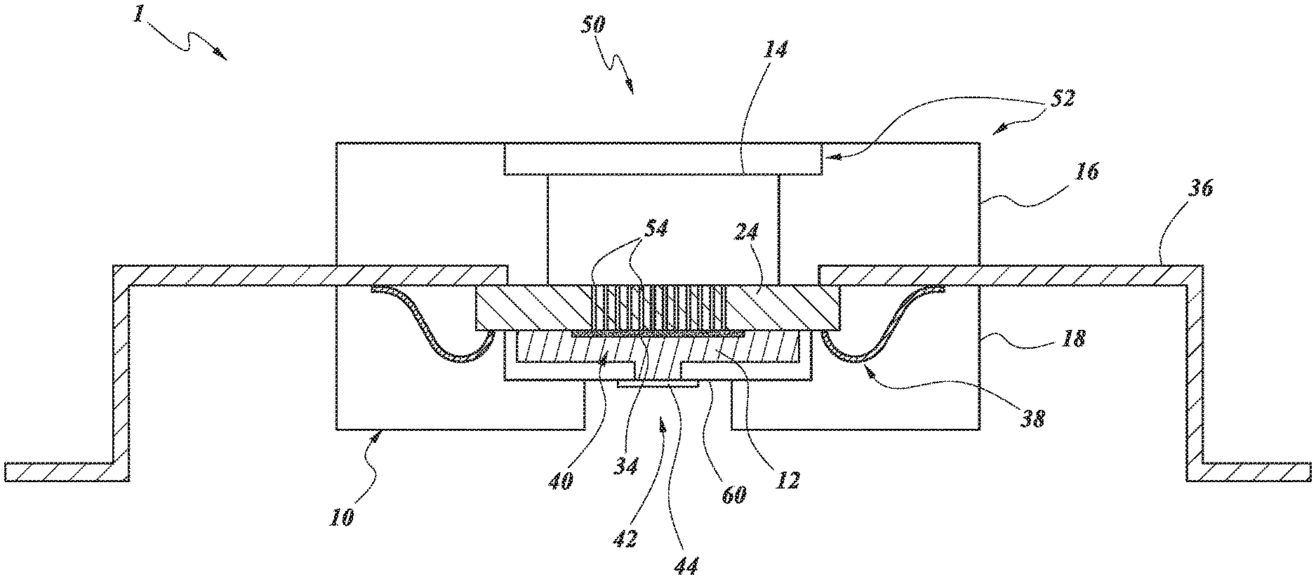
FIG. 1 is a schematic side sectional view of a gas sensor package having a package body at least partially defining first and second chambers, and a first lid and a second lid, according to one embodiment.
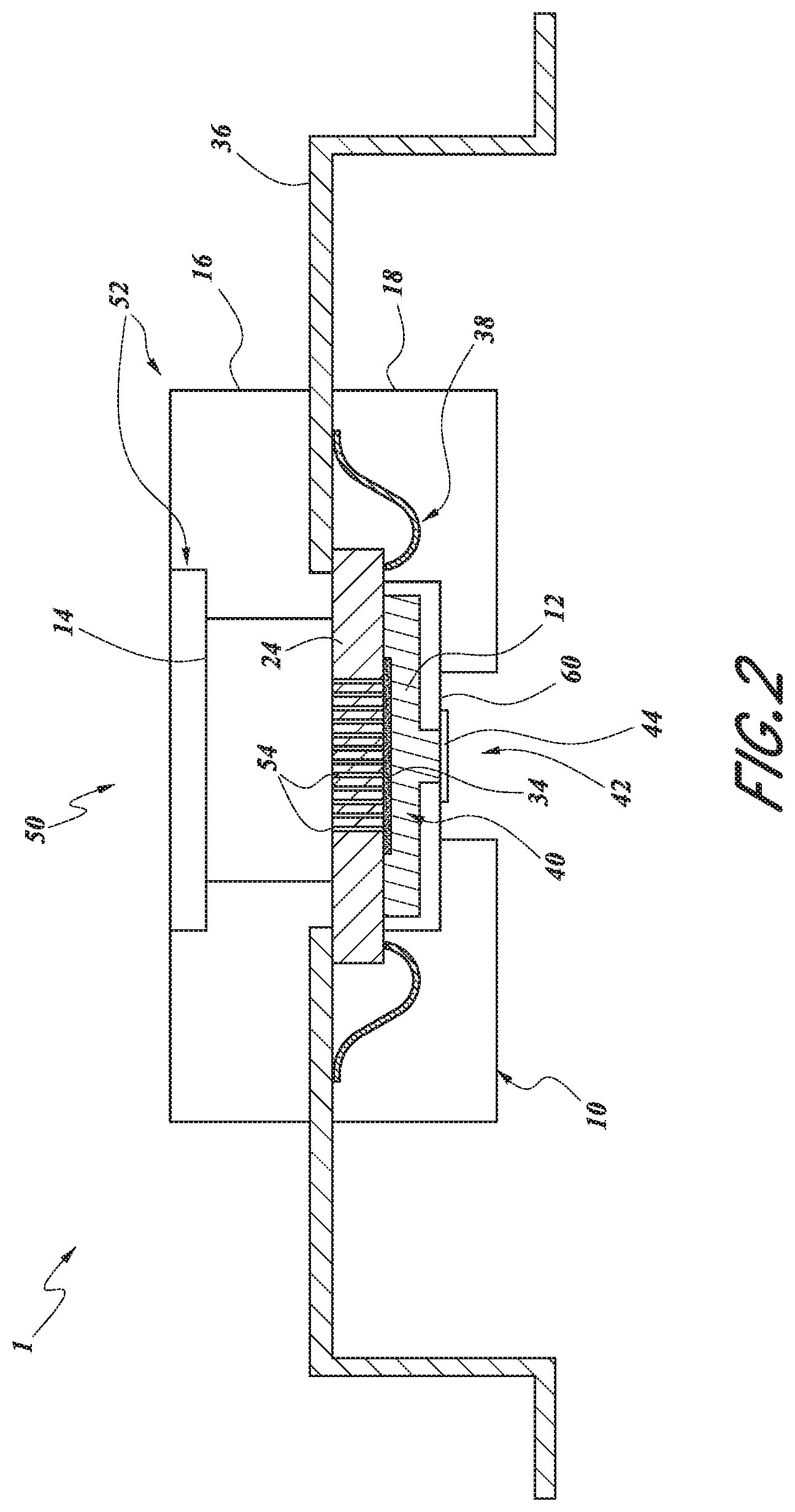
FIG. 2 is a schematic side cross-sectional view of a gas sensor package having a die cap at least defining a first chamber, according to another embodiment.
FIG. 3 is a schematic side cross-sectional view of a gas sensor package with a molding material provided over the die cap, according to another embodiment.
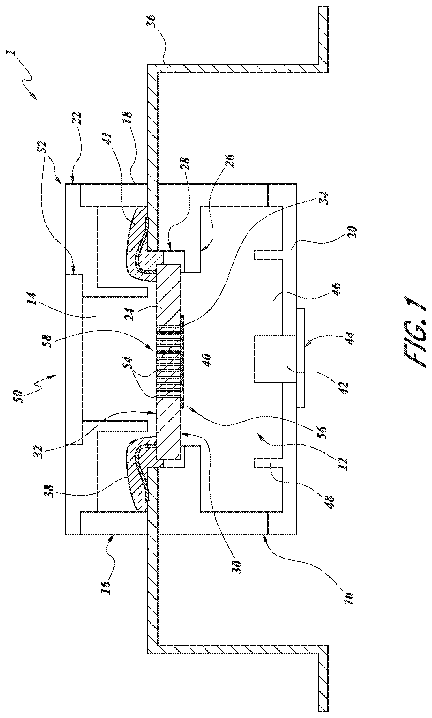
FIG. 4 is a schematic side cross-sectional view of a gas sensor package having a package substrate with a second integrated device die mounted to the package substrate, according to another embodiment.
FIG. 5 is a schematic side cross-sectional view of a gas sensor package having first and second chambers in an outer chamber, according to another embodiment.
FIG. 6 is a schematic side cross-sectional view of a gas sensor package with a sensor die having a through substrate via, according to another embodiment.
FIG. 7 is a schematic side cross-sectional view of a gas sensor package with a die shelf for the sensor die, according to another embodiment.
FIG. 8 is a schematic side sectional view of a sensor die in which a sensor portion and a processor portion are defined in a common unitary structure.
FIG. 9 is a schematic side cross-sectional view of a gas sensor package having a lid that defines a housing for the sensor die and other devices or dies, according to another embodiment.
FIG. 10 is a schematic side cross-sectional view of a gas sensor package having other devices or dies outside of the housing defined by the lid, according to another embodiment.
FIG. 11 is a schematic side cross-sectional view of a gas sensor package, according to another embodiment.
FIG. 12 is a schematic side cross-sectional view of a gas sensor package having a lid that defines the housing for the sensor die and other devices or dies, according to another embodiment.
FIG. 13 is a schematic side cross-sectional view of a gas sensor package having other devices or dies outside of the housing defined by the lid, according to another embodiment.
DETAILED DESCRIPTION
Various embodiments disclosed herein relate to gas sensor packages. For example, the gas sensor packages disclosed herein can enable sensing devices that are smaller and less expensive than conventional sensors. In various embodiments, the gas sensor packages can comprise a housing defining a first chamber and a second chamber. An electrolyte can be provided in the first chamber. A gas inlet can provide fluid communication between the second chamber and the outside environs. The gas inlet can be configured to permit gas to enter the second chamber from the outside environs. An integrated device die can be mounted to the housing. The integrated device die can comprise an amperometric sensor. The integrated device die can comprise a sensing element configured to detect the gas. The integrated device die can have a first side exposed to the first chamber and a second side exposed to the second chamber. The first side can be opposite the second side.
FIG. 1 is a schematic side sectional view of a gas sensor package 1, according to one embodiment. The gas sensor package 1 can include a housing 10 comprising first and second chambers 12, 14, as shown in FIG. 1. The housing 10 can be defined by a molded package body 16 that at least partially delimits the first and/or second chambers 12, 14. For example, as shown in FIG. 1, the package body 16 can comprise a nonconductive molding compound 18. As shown in FIG. 1, the package body 16 can comprise a dual-sided construction. A first lid 20 can be attached (e.g., by way of thermoplastic welding or joining techniques such as thermocompression bonding) to the package body 16 to partially define the first chamber 12. A second lid 22 can be attached (e.g., by way of thermoplastic welding or joining techniques such as thermocompression bonding) to the package body 16 to partially define the second chamber 14.
An integrated device die 24 can be physically mounted to a ledge 26 defined in the package body 16. The die 24 can be disposed between the first and second chambers 12, 14. A die attach or sealant compound 28 can mechanically attach the die 24 to the ledge 26. The integrated device die 24 can comprise an amperometric sensor. The integrated device die 24 can comprise a sensing element 34 on a first side 30 of the die 24. For example, the sensing element 34 can be adhered or laminated to the die 24. In various embodiments, the sensing element 34 can comprise platinum black or other types of electrodes used in electrochemical applications. In some embodiments, the sensing element 34 can comprise ruthenium black, iridium black, carbon, gold black, or gold. For example, in various embodiments, platinum black can be used for sensing carbon monoxide and hydrocarbons, such as alcohol, etc. In various embodiments, sintered platinum or iridium can be used for sensing hydrogen gas. Gold black may be used to detect sulfur containing compounds, such as hydrogen sulfide. In some embodiments, stabilized iridium may be used to detect gases such as ammonia and hydrazine.
In some embodiments, the sensing element 34 can electrically connect to corresponding contact pads (not shown) on the die 24. In other embodiments, the sensing element 34 can be formed as part of the die 24. In various embodiments, the sensing element 34 can be printed on a sensor part of the die 24 over capillaries or channels. In some embodiments, a cap can be attached over the sensing element 34, for example, to protect the sensing element 34. Furthermore, the die 24 can comprise other active circuitry and electrical interconnects connecting the active circuitry to the sensing element 34 for preprocessing signals detected by the sensing element, in some embodiments. As shown in FIG. 1, contact pads on a second side 32 of the die 24 can electrically connect the active circuitry or the interconnects to leads 36 of the package 1, e.g., by way of wire bonds 38. The wire bonds 38 may comprise gold or aluminum bonding wires, and may be bonded to the pads of the die 24 at room temperature to ensure that temperature limits of the sensing element are not exceeded. An encapsulant 41 or glob-top can be applied over the wire bonds 38 to protect the wire bonds 38 and/or electrically isolate the wire bonds 38. In other embodiments, the die 24 can be flip chip mounted to a substrate or package body, e.g., by way of solder balls or anisotropic conductive film (ACF), but such an arrangement may introduce additional costs as compared with wire bonding.
As shown in FIG. 1, an electrolyte 40 can be provided in the first chamber 12 of the package 1. The electrolyte 40 can comprise any suitable type of electrolyte for gas sensing applications, including, e.g., acids, such as a solution comprising sulfuric acid (e.g., a 40% sulfuric acid solution), bases, salts, organic electrolytes, gel electrolytes, polymer electrolytes, etc. In other embodiments, the electrolyte 40 can comprise other types of liquids (including gels) or solid electrolytes. In various embodiments, a combination of liquid and solid can be used for the electrolyte 40, such as water and a conductive polymer, for example, a sulfonated tetrafluoroethylene based fluoropolymer-copolymer (e.g., Nafion.RTM. manufactured by DuPont USA). For example, in some embodiments, the first lid 20 can be attached to a lower portion of the package body 16 as explained above. The electrolyte 40 can be flowed into the first chamber 12 by way of an opening 42. A sealing cap 44 can be provided over the opening 42 to seal the electrolyte 40 in the first chamber 12. In FIG. 1, the sensing element 34 can be exposed to the electrolyte 40 (for example, contacting the electrolyte) and/or at least partially disposed in the first chamber 12.
The first chamber 12 can also include a wicking material 46 to ensure that the electrolyte 40 contacts the sensing element 34. The wicking material 46 can comprise any suitable type of material, including, for example, a glass fiber matting in the first chamber 12. In various embodiments, the wicking material 46 can comprise a discrete component that is provided in the first chamber 12. In some embodiments, the wicking material 46 may comprise an open-cell foam that can be dispensed in fluid form to fill the first chamber 12. For example, projections 48 shown in FIG. 1 can cooperate with the wicking material 46 to press or draw the electrolyte 40 upwards to maintain contact with the sensing element 34. In the absence of the wicking material 46, there may be an air gap below the sensing element 34 such that the electrolyte 40 does not contact the sensing element 34 along its area. The wicking material 46 may also prevent splashing of the electrolyte 40 during dispensing and capping of the sealing cap 42. Thus, providing the wicking material 46 can improve the sensing capabilities of the gas sensor package 1 by maintaining contact between the electrolyte 40 and the sensing element 34.
The second chamber 14 can fluidly communicate with the outside environs by way of a gas inlet 50. As shown in FIG. 1, one or more filters 52 can be provided across the gas inlet 50. The filter(s) 52 can comprise mechanical barriers configured to prevent debris from entering the second chamber 14. In some embodiments, the filter(s) 52 can additionally or alternatively be configured to filter out organic compounds or other undesirable contaminants. Two filters 52 are illustrated in FIG. 1, but any suitable number and type of filters can be provided across the gas inlet 50 between the second chamber 12 and the outside environs. The filter(s) 52 may be provided before or after the second lid 22 is attached to the package body 16. The filter(s) 52 may be any suitable type of filter, such as a graphite filter, a polytetrafluoroethylene (PTFE) anticondensation filter or dust filter.
During operation, gas(es) can enter the second chamber by way of the gas inlet 50 and the filter(s) 52. As shown in FIG. 1, the second side 32 of the die 24 is exposed to the second chamber 14 and to the gas(es) entering the second chamber 14. The die 24 can comprise one or a plurality of channels 54 or capillaries formed through the die 24, e.g., from the second side 32 of the die 24 exposed to the second chamber 14 to the first side 30 of the die 24 on which the sensing element 34 is mounted or otherwise disposed. As shown in FIG. 1, the sensing element 34 can be disposed on a portion of the first side 30 of the die 24, and another portion of the first side 30 of the die 24 can be exposed to the electrolyte 40 in the first chamber 12. The die 24, therefore, can comprise a material resistant to the electrolyte 40 (e.g., an acid) such that the electrolyte 40 does not damage the die 24. Thus, the first side 30 of the die 24 can comprise a "wet" side 56 of the die 24, and the second side 32 of the die 24 can comprise a "dry" side 58 of the die 24. In various embodiments, the die 24 can comprise a semiconductor material such as silicon. Importantly, the die attach material or sealant, in cooperation with the integrated device die 24, can seal and/or fluidly separate the first chamber 12 from the second chamber 14 such that the electrolyte 40 does not enter the second chamber 14 from the first chamber 12. The die 24 can act as a barrier between the electrolyte 40 in the first chamber 12 and the gas(es) in the second chamber 14.
Gas passing through the channels 54 can contact the dry side 58 of the sensing element 34 on an opposite side of the wet side 56 of the sensing element 34, which contacts the electrolyte 40. In some embodiments, the gas can diffuse into the sensing element 34 of the integrated device die 24 (e.g., amperometric sensor die) and the integrated device die 24 can generate current, for example, as a consequence of chemical reactions of the gas at an interface between the sensing electrode 34 and the electrolyte 40 in the first chamber 12. A magnitude of the generated current is proportional to a gas concentration near the sensing element 34. Beneficially, the embodiment of FIG. 1 can enable the production of smaller-scale gas sensor packages that are simple and less expensive as compared with conventional gas sensors.
In some embodiments, the die 24 can include through substrate vias (TSVs) from the first side 30 of the die 24 that receives the sensing element 34 to the second side 32 opposite the first side 30, as illustrated, for example, in FIGS. 6 and 9-11. The TSVs on the second side can be connected to the wire bonds 38 to make electrical connection with the leads 36.
FIG. 2 is a schematic side cross-sectional view of a gas sensor package 1, according to another embodiment. Unless otherwise noted, the components of FIG. 2 may be the same as or generally similar to like-referenced components of FIG. 1. Further, the package 1 may operate generally similar to the package 1 of FIG. 1, in that gas can enter the gas inlet 50 and pass from the second chamber 14 and through the channels 54 to the first chamber 12. Current generated by the sensor die 24 can be measured, and the measured current can be representative of one or more target gas species. For example, as with FIG. 1, the gas sensor package 1 can comprise a first chamber 12 in which an electrolyte 40 is disposed and a second chamber 14 that fluidly communicates with the outside environs by way of a gas inlet 50 and one or more filters 52 disposed over the gas inlet 50. Additionally, unlike the embodiment of FIG. 1, in which the package body 16 and a package lid 20 define the first chamber 12, in the embodiment of FIG. 2, a die cap 60 can be attached to or formed with the integrated device die 24. The die cap 60 can define a smaller first chamber 12 than in the embodiment of FIG. 1, which can beneficially enable a smaller gas sensor package.
In the embodiment of FIG. 2, moreover, the package body 16 can be molded about the illustrated components by way of film assist molding (FAM), which combines high volume molding processes with the ability to leave an opening 42 such as that shown in FIG. 2. For example, in some embodiments, the integrated device die 24, the die cap 60, and the leads 36 can be molded using FAM, and the opening 42 may be left open by providing a tip or insert on the bottom of the die cap 60 such that the opening 42 is not molded. After molding, the electrolyte 40 (e.g., sulfuric acid) can flow through the opening 42 and into the first chamber 12. The sealing cap 44 (or a sealant or adhesive) can be provided over the opening in the die cap 60 to seal the electrolyte 40 in the first chamber 12, e.g., by way of a suitable sealant or adhesive. Beneficially, therefore, the gas sensor package 1 of FIG. 2 can utilize low cost molding techniques and materials at any suitable temperature, since the electrolyte 40 can be provided after molding, but assembly is simplified by omitting separate lid attachment for the first chamber 12. Moreover, the die 24 can be supported by, and at least partially embedded in, the package body 16 which may be defined by the molding compound 18. There may be no separate die paddle in various embodiments. For example, as shown in FIG. 2, the die 24 may be supported by the package body 16 and distal portions of the leads 36. The package body 16 can at least partially embed end portions of the die 24 so as to support the die 24. In some embodiments, the die 24 can be adhered to the distal portions of the leads 36. Further, as shown in FIG. 2, the molding compound 18 can be defined to include recesses for receiving the filter(s) 52. In some embodiments, the filter(s) 52 may be flush with or below the top surface of the package body 16. In some embodiments, one or more filter(s) 52 may protrude above the top surface of the package body 16.
Further, in embodiment of FIG. 2, electrical connections (e.g., the wire bonds 38) between the die 24 and the lead 36 may be covered with the molding compound 18 that at least partially defines the package body 16. Therefore, protection for the wire bonds 38 and/or electrical isolation of the wire bonds 38 may be provided without the separate encapsulant 41 or glob-top shown in FIG. 1.
FIG. 3 is a schematic side cross-sectional view of a gas sensor package 1, according to another embodiment. Unless otherwise noted, the components of FIG. 3 may be the same as or generally similar to like-referenced components of FIGS. 1-2, and may operate or function in a generally similar manner. Unlike the embodiment of FIG. 2, in which the sealing cap 44 can be applied after filling the first chamber 12 with the electrolyte 40 either before or after molding, in FIG. 3, the electrolyte 40 can be provided in the first chamber 12 prior to the molding of the package body 16. For example, the first chamber 12 defined at least in part by the die cap 60 can be filled with the electrolyte 40 at the wafer level, and the sealing cap 44 can be applied over the opening 42 in the die cap 60. The molding compound 18 can be provided over the die cap 60 and the sealing cap 44 in FIG. 3. In some embodiments, therefore, the die cap 60, the electrolyte 40, and the sealing cap 44 can be applied to a wafer having multiple integrated device regions. The integrated device regions can be singulated to define a plurality of dies with the electrolyte 40 provided before singulation. In still other embodiments, the electrolyte 40 may be provided in the die cap 60 chamber after singulation of the wafer.
FIG. 4 is a schematic side cross-sectional view of a gas sensor package 1, according to another embodiment. Unless otherwise noted, the components of FIG. 4 may be the same as or generally similar to like-referenced components of FIGS. 1-3, and may operate or function in a generally similar manner. For example, as with FIGS. 1-3, the package of FIG. 4 can comprise a first chamber 12 and a second chamber 14 on opposing sides of the integrated device die 24. Moreover, the package 1 can comprise a molded package body 16 (which may be formed by a FAM technique). The package body 16 can be applied over or coupled with a package substrate 62, which may comprise a laminate substrate such as a printed circuit board (PCB) substrate, a ceramic substrate, or any other suitable type of substrate. The package substrate 62 can comprise an opening 64 that can at least partially define the gas inlet 50. As shown in FIG. 4, the opening 64 and the gas inlet 50 can be disposed on a bottom side 68 of the gas sensor package 1. One or more filters 52 can be coupled to the package substrate 62 over the opening 64. The second chamber 14, which can be in fluid communication with gas(es) in the outside environs by way of the gas inlet 50, can be defined at least in part by the opening 64 in the package substrate 62. The integrated device die 24 can be disposed over the opening 64 and the second chamber 14.
A lid 20 can be coupled to or embedded within the package body 16. For example, as explained above, FAM techniques can enable the formation of openings or voids 65 in the molding compound 18 of the package body 16. The lid 20 can be connected to the package body 16 within openings or voids defined in the molding compound 18. The lid 20 and the package body 16 can define an outer chamber 70 in which the integrated device die 24 is disposed. The die cap 60 can be mounted to the integrated device die 24 over the sensing element 34 to define the first chamber 12 in which the electrolyte 40 is provided. In some embodiments, the die cap 60 can be pre-filled with the electrolyte 40, and the sealing cap 44 can seal the first chamber 12 of the die cap 60 during wafer-level assembly. In other embodiments, the first chamber 12 of the die cap 60 can be filled with electrolyte 40 during packaging, e.g., after the die 24 is mounted to the package substrate 62 but before application of the lid 20. As with the above embodiments, the integrated device die 24 and associated die attach materials or sealants can act as a barrier or seal between the electrolyte 40 in the first chamber and the gas(es) in the second chamber 14.
Further, as shown in FIG. 4, a second integrated device die 72 can be mounted to the package substrate 62 and can be laterally offset relative to the integrated device die 24 coupled with the sensing element 34. In FIG. 4, the second die 72 can be embedded in the molding compound of the package body 16, which can beneficially enable standard high temperature packaging and molding techniques. The device die 24 and sensing element 34 can be packaged in a separate, low temperature packaging stage so as to mitigate damage to the sensing element as a result of high temperature processing. The integrated device die 24 can be wire bonded to the substrate 62, and the second integrated device die 72 can electrically communicate with the integrated device die 24 by way of conductive traces embedded in or on the package substrate 62 (e.g., by way of flip-chip or wire bonding interconnections, which are not shown in FIG. 4). In various embodiments, the wire bonds 38 may be protected by a glob-top or molding material (see, for example, FIG. 1). In other embodiments, the wire bonds 38 may not be protected by a glob-top or molding material. In some embodiments, the second die 72 can process signals transduced by the integrated device die 24 with the sensing element 34. Other devices (e.g., passives) can be similarly mounted on the package substrate 62 (e.g., laminate substrate) and communicate with the integrated device (sensor) die 24 and/or the second integrated device die 72 through the the package substrate 62 (e.g., laminate substrate) or directly. The packaging substrate 62 includes leads 37 on the lower surface thereof to facilitate electrical connection to larger electronic systems, e.g., by way of a mother board, such as a printed circuit board, or PCB.
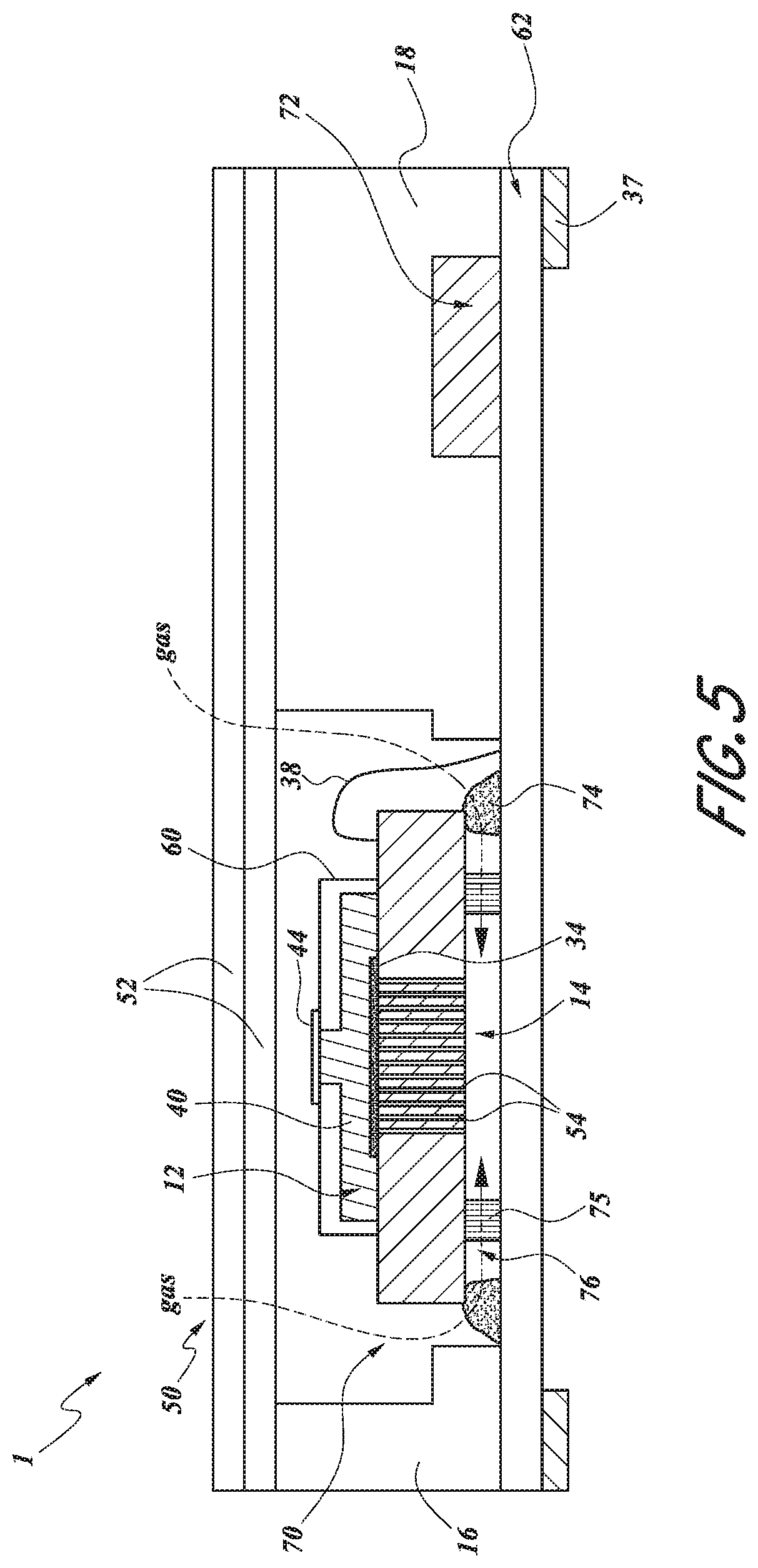
FIG. 5 is a schematic side cross-sectional view of a gas sensor package 1, according to another embodiment. Unless otherwise noted, the components of FIG. 5 may be the same as or generally similar to like-referenced components of FIGS. 1-4, and may otherwise operate or function in a generally similar manner. Unlike the embodiment of FIG. 4, for example, the gas inlet 50 can be provided at the top side of the package 1. The filter(s) 52 can be provided over an aperture defined in the molding compound 18 (e.g., which may be formed using a FAM technique) and over the gas inlet 50. As shown, the die 24 can be mounted to the package substrate 62 by way of a die attach material 74. Further, a standoff structure 75 can be provided to space the bottom surface of the die 24 vertically offset from the top surface of the package substrate 62. Gas can enter the outer chamber 70 of the package 1 through the gas inlet 50 and filters 52, and can pass laterally through lateral channels 76 to enter the second chamber 14. Thus, the standoff structure 75, the integrated device die 24, and the package substrate 62 can define the second chamber 14 in the embodiment of FIG. 5, which is in open fluid communication with the outer chamber 70. The lateral channels 76 within the standoff structure 75 can provide fluid communication between the outer chamber 70 and the second chamber 14. In various embodiments, the lateral channels 76 can be defined by etching laterally through the standoff structure 75 (which may comprise silicon). As with the embodiments described above, the die 24, the die cap 60 and the sealing cap 44 can define the first chamber 12 in which the electrolyte 40 is disposed. Thus, in FIG. 5, the second chamber 14 can be disposed between the die 24 and the package substrate 62. The first chamber 12 can be disposed between the die 24 and the gas inlet 50 or filters 52. In some embodiments the lateral channels 76 may comprise the second chamber 14.
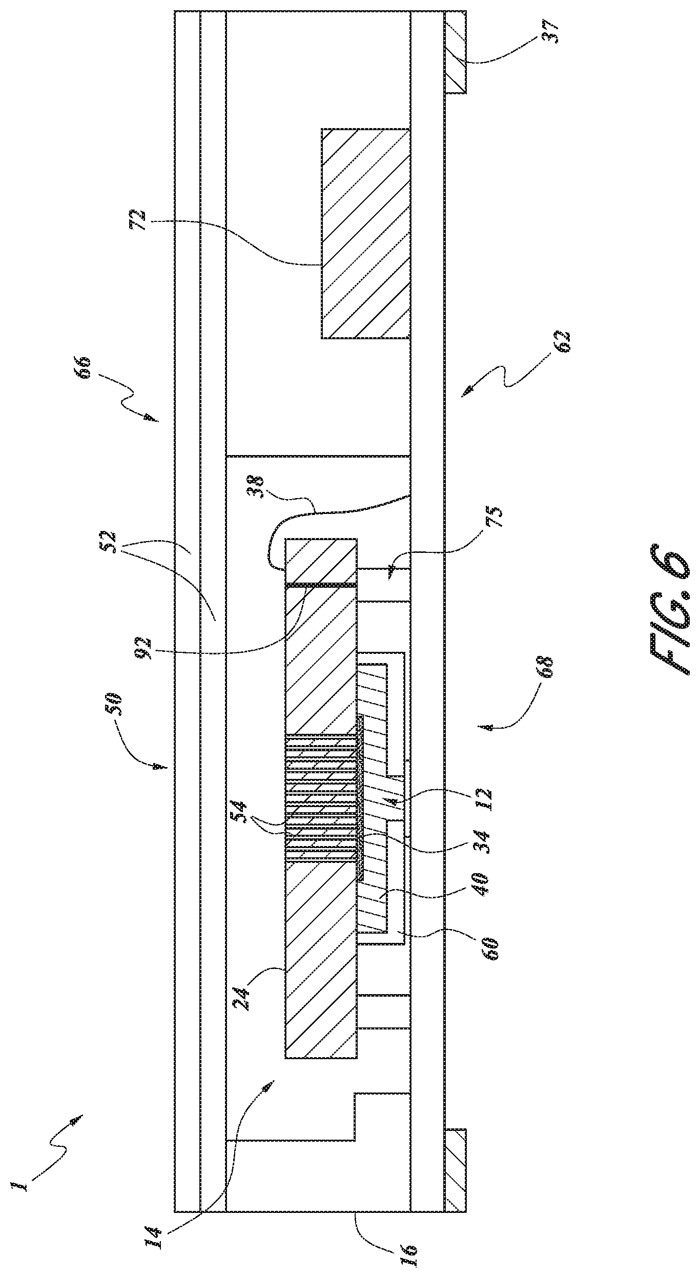
FIG. 6 is a schematic side cross-sectional view of a gas sensor package 1, according to another embodiment. Unless otherwise noted, the components of FIG. 6 may be the same as or generally similar to like-referenced components of FIGS. 1-5, and may operate or function in a generally similar manner. As with the embodiment of FIG. 5, the gas inlet 50 and filter(s) 52 can be provided at a top side 66 of the package 1. Unlike the embodiment of FIG. 5, however, the outer chamber can directly serve as the second chamber 14, and the first chamber 12 can be disposed nearer the bottom side 68 of the package 1. One or more die supports 75 can support the die 24 above the package substrate 62 to improve the structural support of the die 24 during manufacturing and/or use, and to provide a space which can accommodate the thickness of the die cap 60 and first chamber 12. As shown in FIG. 6, the first chamber 12 can be disposed between the die 24 and the package substrate 62. As shown in FIG. 6, one or more through-silicon vias (TSVs) 92 can be provided to provide electrical communication between front and back surfaces of the die 24.
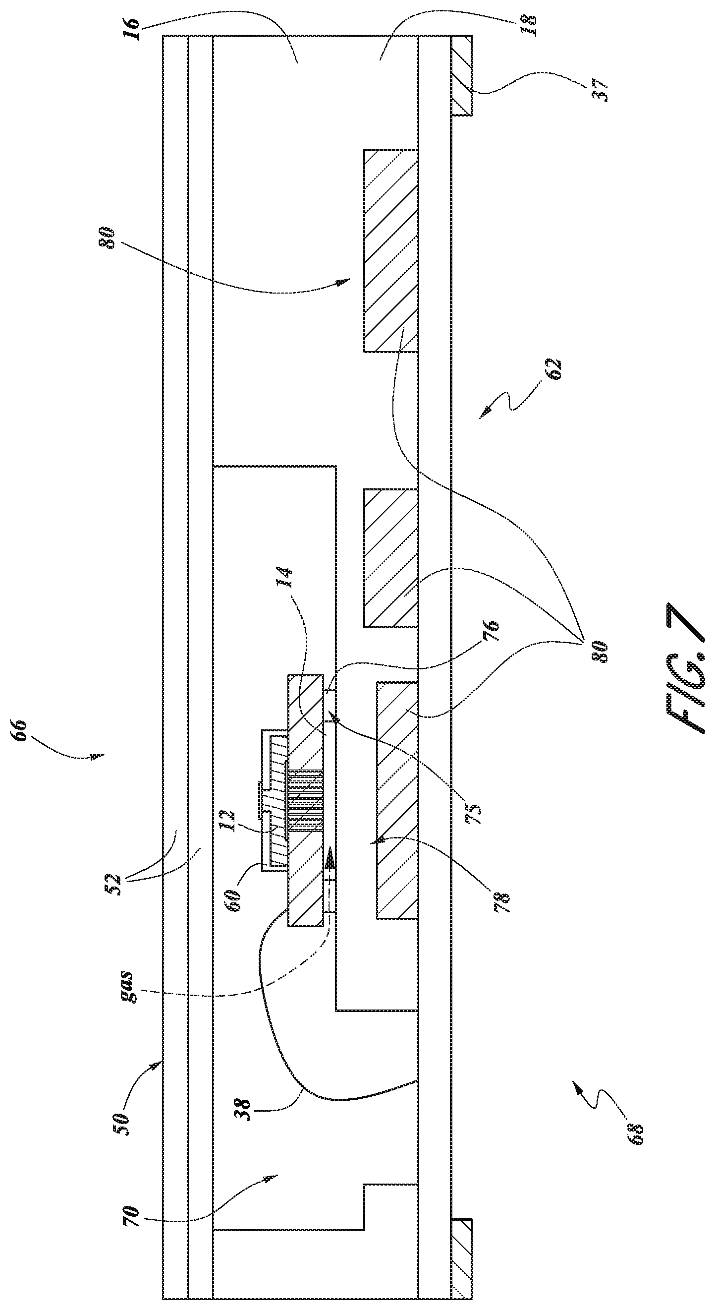
FIG. 7 is a schematic side cross-sectional view of a gas sensor package 1, according to another embodiment. Unless otherwise noted, the components of FIG. 7 may be the same as or generally similar to like-referenced components of FIGS. 1-6, and may operate or function in a generally similar manner. The package 1 of FIG. 7 may be similar to the package 1 shown in FIG. 5, e.g., the second chamber 14 may be disposed between the die 24 and the package substrate 62, or nearer the bottom side 68 of the package 1. The first chamber 12 and the electrolyte 40 may be disposed between the die 24 and the gas inlet 50, or nearer the top side 66 of the package 1. Unlike the embodiment of FIG. 5, however, in FIG. 7, the integrated device die 24 can be mounted over a die shelf 78 defined at least in part by the molding compound 18 of the package body 16. As shown in FIG. 7, the package body 16 can be overmolded over one or more additional integrated device dies and/or other electronic components 80 (e.g., passives) to define the die shelf 78. The integrated device die 24 with the sensing element 34 can be mounted to the die shelf 78 over the one or more additional devices or dies 80. The integrated device (sensor) die 24 can be electrically connected to the laminate package substrate 62, such as by way of the illustrated bond wires 38, for communication with the embedded dies and/or other electronic components 80.
As with FIG. 5, in FIG. 7, a standoff structure 75 can be provided to vertically offset the die 24 relative to the die shelf 78. Lateral channels 76 can be defined in the standoff structure 75 and/or the die shelf 78 during molding to enable fluid communication between the outer chamber 70 and the second chamber 14. Thus, gas(es) can enter the outer chamber 70 through the gas inlet 50 and filter(s) 52. The gas(es) can pass through the lateral channels 76 in the standoff structure 75 and/or the die shelf 78 to enter the second chamber 14. Beneficially, the embodiment of FIG. 7 can enable a lower package footprint since the integrated device die 24 can be stacked on the overmolded additional devices or dies 80.
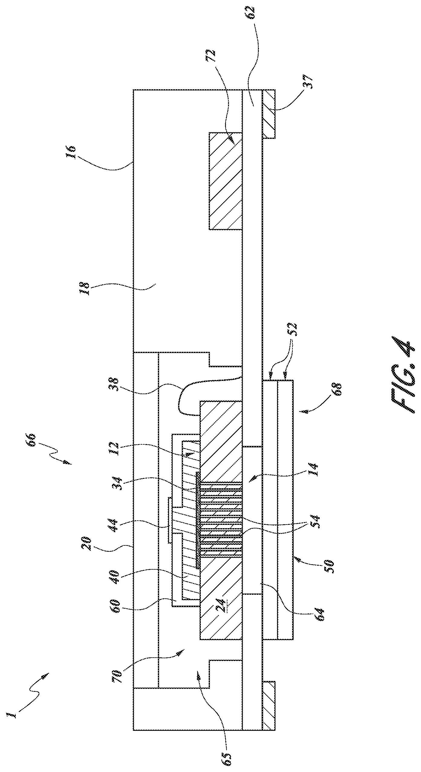
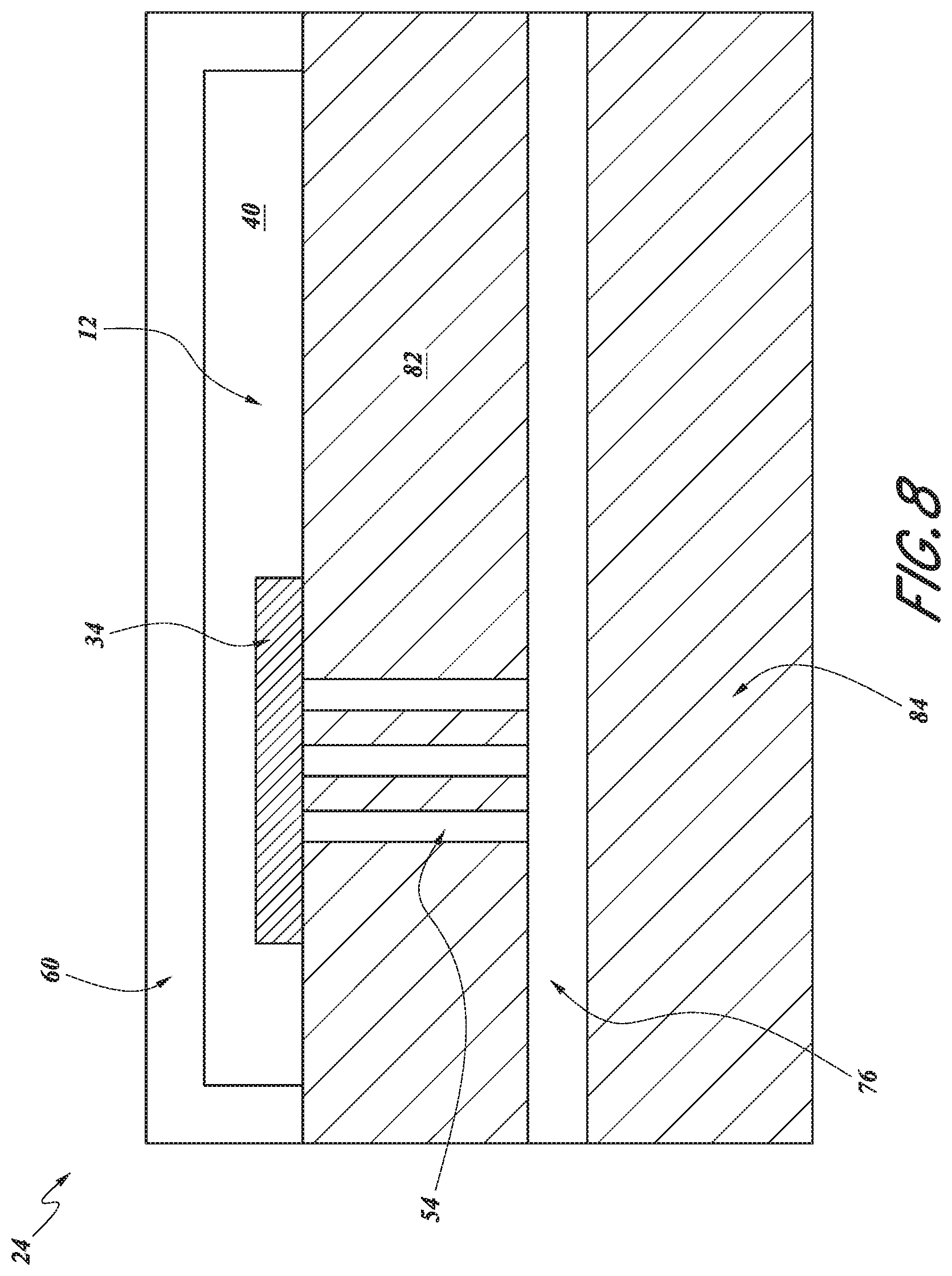
FIG. 8 is a schematic side sectional view of a sensor die 24 in which a sensor portion 82 and a processor portion 84 are defined in a common unitary structure. Unless otherwise noted, the components of FIG. 8 may be the same as or generally similar to like-referenced components of FIGS. 1-7. For example, as shown in FIG. 8, a sensing element 34 can be applied (e.g., printed or otherwise coupled) on the sensor portion 82 of the die 24 over the gas channels 54. An electrolyte 40 can be provided in the first chamber 12. The sensor die 24 of FIG. 8 can be used in conjunction with any of the packages disclosed herein. The sensor portion 82 and processor portion 84 can be made from the same substrate, e.g., the same wafer. For example, active processing circuitry can be defined in the processor portion 84, and additional routing circuitry can be defined in the sensor portion 82. A lateral chamber 76 or channel can be defined between the processor portion 84 and the sensor portion 82. The lateral chamber 76 or channel can provide a gas inlet for gas to enter the vertical channels 54 to interact with the sensing element 34. In some embodiments, the lateral chamber 76 can serve as the second chamber 14 to provide fluid communication to one side of the sensor portion of the die 24. In other embodiments, a chamber outside of the die 24 can serve as the second chamber 14.
In various embodiments, the lateral chamber 76 or channel can be defined by etching. For example, a sacrificial material can be deposited on the processor portion 84, and an etchant can be provided through the vertical channels 54 to etch the sacrificial material in the lateral chamber 76 or channel. The lateral channels 76 can be etched by wet etching, dry etching, or any other suitable method. In various embodiments, the sensor die 24 may comprise pre-formed channels, and the sensor die 24 and an application specific integrated circuit (ASIC) can be stacked together, e.g., by a die attach material. Additional details of the sensor die 24 shown in FIG. 8 may be found throughout U.S. Patent Publication No. US 2018-0059044, the entire contents of which are hereby incorporated by reference herein in their entirety and for all purposes.
FIG. 9 is a schematic side cross-sectional view of a gas sensor package 1, according to another embodiment. Unless otherwise noted, the components of FIG. 9 may be the same as or generally similar to like-referenced components of FIGS. 1-8, and may operate or function in a generally similar manner. In the embodiment of FIG. 9, the gas sensor package 1 can comprise a package lid 86 that at least partially defines the second chamber 14 that communicates with the gas inlet 50. As shown in FIG. 9, the sensor die 24 can be supported by a package substrate 62 (e.g., a laminate substrate) by way of intervening die supports 87 or dams. The die supports 87 or dams can comprise L- or T-shaped structures (e.g., molded dams) to restrict the bleed out of die attach material between the sensor die 24 and the package substrate 62, and to provide support to the die 24. However, it should be understood that the die supports 87 or dams can comprise other shapes suitable.
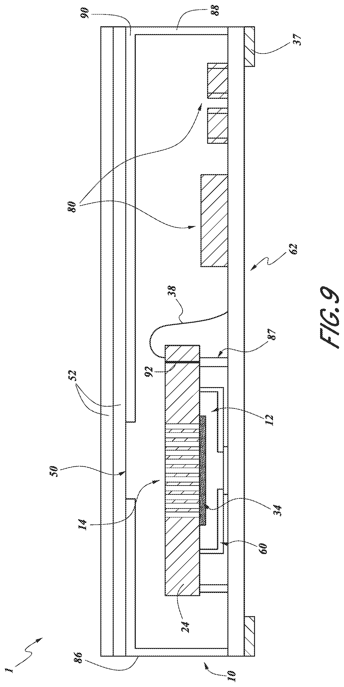
The package 1 can serve as a laminate-based system-in-package. As above, the electrolyte 40 can be provided in the first chamber 12 defined at least in part by the die cap 60. The sensor die 24 can be inverted in the illustrated embodiment, e.g., to reduce the distance between the gas inlet 50 and the sensor die 24 and sensing element 34. In the illustrated embodiment, the package lid 86 can be provided over the sensor die 24 and other dies, packages, and/or passive components 80. The package lid 86 can comprise a shaped lid, e.g., with one or more vertical legs 88 that support a horizontal upper lid portion 90. One or more filters 52 can be coupled to the lid 86. In FIG. 9, the filters 52 are disposed over the horizontal upper lid portion 90 of the package lid 86. However, in some embodiments, the filters 52 may be disposed inside the package lid 86 (e.g., under the lid portion 90), or both inside and outside of the package lid 86 (e.g., over and under the lid portion 90). The gas inlet 50 can comprise a port hole formed in the lid 86, e.g., the upper portion of the lid 86.
As explained above, the package lid 86 can at least partially define the second chamber 14. In the embodiment of FIG. 9, the sensor die 24 and other dies, packages, or passive components 80, including processor dies (e.g., ASICs) may also be disposed in the second chamber 14 defined at least in part by the lid 86. As explained above, the bonding wires electrically connecting the sensor die 24 or other dies, packages, or passive components 80 to the package substrate 62 may be protected by a polymer or glob-top. In other embodiments, the bonding wires may be exposed to the second chamber 14. In various embodiments, the filters 52 can be applied as sheets to the lid 86, and can protrude above the package body or housing 10. The filter(s) 52 can be applied to the lid 86 before or after attaching the lid 86 to the package substrate 62, according to various embodiments. In still other embodiments, the package lid 86 can comprise one or more recesses sized and shaped to receive and/or support the filter(s) 52. The filter(s) 52 can be compression fit and/or glued to the lid 86 to prevent gas leaks. In various embodiments, the filter(s) 52 can comprise a hydrophobic and/or dust film to reduce the risks of exposing the package 1 to moisture. Further, as shown in FIG. 9, one or more through-silicon vias (TSVs) 92 can be provided to provide electrical communication between front and back surfaces of the die 24.
FIG. 10 is a schematic side cross-sectional view of a gas sensor package 1, according to another embodiment. Unless otherwise noted, the components of FIG. 10 may be the same as or generally similar to like-referenced components of FIG. 9, and may operate or function in a generally similar manner. Unlike the embodiment of FIG. 9, however, in FIG. 10, the lid 86 may be disposed over the sensor die 24, but the other dies, packages, and/or passive components 80 may be mounted to the package substrate 62 and disposed outside the lid 86 and the second chamber 14.
FIG. 11 is a schematic side cross-sectional view of a gas sensor package 1, according to another embodiment. Unless otherwise noted, the components of FIG. 11 may be the same as or generally similar to like-referenced components of FIGS. 9-10, and may operate or function in a generally similar manner. Unlike the embodiments of FIGS. 9-10, as shown in FIG. 11, the one or more filter(s) 52 can be provided on an inner surface of the lid 86, as opposed to on an outer surface of the lid (such as is shown in FIGS. 9-10). Furthermore, in the embodiment of FIG. 11, the filter(s) 52 may contact at least a portion the surface of the sensor die 24. In other embodiments, the lid 86 and filter(s) 52 may stand off from the sensor die 24, such that the second chamber 14 of the package 1 may also be defined by the lid 86 in a manner similar to that shown in FIGS. 9-10. The wire bond 38 can make electrical connection between the die 24 and the package substrate 62. In some other embodiments, the die supports 87 may make electrical connection between the sensor die 24 and the substrate 62. In the embodiment of FIG. 11, gas can pass through the gas inlet 50, through the gas channels 54, and into the first chamber 12. Current generated by the die 24 can be proportional to a gas concentration of the gas, which can be used to identify the gas.
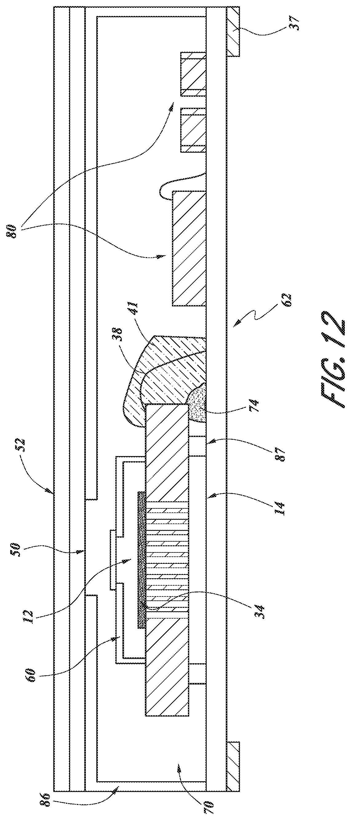
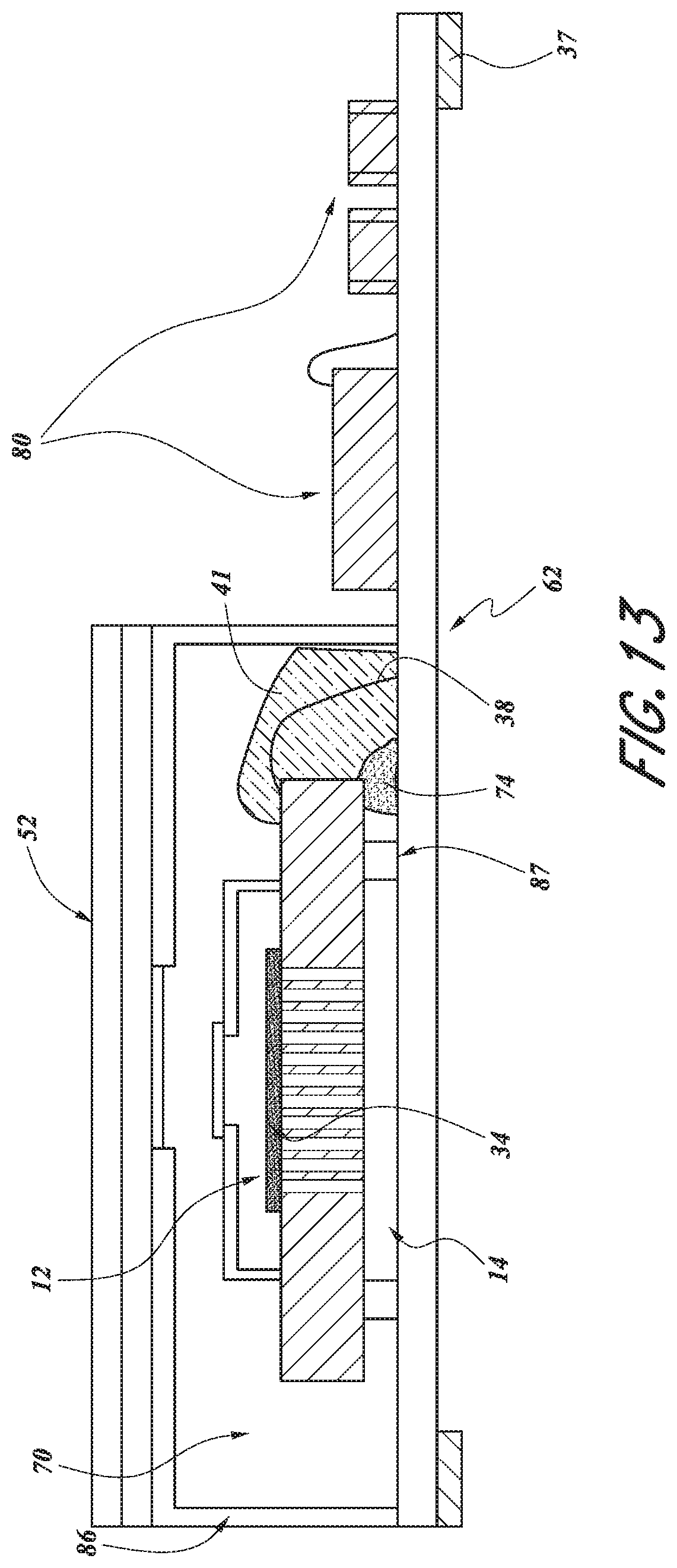
FIG. 12 is a schematic side cross-sectional view of a gas sensor package 1, according to another embodiment. FIG. 13 is a schematic side cross-sectional view of a gas sensor package 1, according to another embodiment. Unless otherwise noted, the components of FIGS. 12-13 may be the same as or generally similar to like-referenced components of FIGS. 9-10, respectively. For example, in FIG. 12, the package lid 86 can be provided over the sensor die 24 and over other dies (such as Application Specific Integrated Circuit, or ASIC, dies), packages, and/or passive components 80. In FIG. 13, the package lid 86 can be provided over the sensor die 24, and the other dies (e.g., ASIC die(s)), packages, and/or package components 80 can be provided outside the lid 86 and the second chamber 14. Unlike in FIGS. 9-10, however, in FIGS. 12-13, respectively, the sensor die 24 can be inverted as compared with FIGS. 9-10. As shown in FIG. 12, for example, the gas can pass through the gas inlet 50 into the second chamber 14. For example, the gas can pass through openings (not shown) in the die support 87 or dam to enter the second chamber 14.
As illustrated in FIGS. 12 and 13, the encapsulant 41 or glob-top can be disposed over the wire bonds 38. The embodiment of FIG. 13 can be beneficial for capturing the encapsulant 41 within the outer chamber 70 so as to prevent the encapsulant 41 to reach the other dies, packages, and/or passive components 80.
Although this invention has been disclosed in the context of certain embodiments and examples, it will be understood by those skilled in the art that the present invention extends beyond the specifically disclosed embodiments to other alternative embodiments and/or uses of the invention and obvious modifications and equivalents thereof. In addition, while several variations of the invention have been shown and described in detail, other modifications, which are within the scope of this invention, will be readily apparent to those of skill in the art based upon this disclosure. It is also contemplated that various combinations or sub-combinations of the specific features and aspects of the embodiments may be made and still fall within the scope of the invention. It should be understood that various features and aspects of the disclosed embodiments can be combined with, or substituted for, one another in order to form varying modes of the disclosed invention. Thus, it is intended that the scope of the present invention herein disclosed should not be limited by the particular disclosed embodiments described above, but should be determined only by a fair reading of the claims that follow.
* * * * *
References
-
nanowerk.com/spotlight/spotid=17875.php
-
sciencedaily.com/releases/2010/09/100912151548.htm
-
-
igpg.com.cn/Products/Online_pH_ORP_Sensor2/75.html
-
aliexpress.com/store/product/Glass-PH-sensor-PH-electrode-for-pipe-on-stallation-ph-G2008/1040787_32259217887.html
D00000
D00001
D00002
D00003
D00004
D00005
D00006
D00007
D00008
D00009
D00010
D00011
D00012
D00013
XML
uspto.report is an independent third-party trademark research tool that is not affiliated, endorsed, or sponsored by the United States Patent and Trademark Office (USPTO) or any other governmental organization. The information provided by uspto.report is based on publicly available data at the time of writing and is intended for informational purposes only.
While we strive to provide accurate and up-to-date information, we do not guarantee the accuracy, completeness, reliability, or suitability of the information displayed on this site. The use of this site is at your own risk. Any reliance you place on such information is therefore strictly at your own risk.
All official trademark data, including owner information, should be verified by visiting the official USPTO website at www.uspto.gov. This site is not intended to replace professional legal advice and should not be used as a substitute for consulting with a legal professional who is knowledgeable about trademark law.