Bowing semiconductor wafers
Abas
U.S. patent number 10,720,351 [Application Number 16/119,776] was granted by the patent office on 2020-07-21 for bowing semiconductor wafers. This patent grant is currently assigned to SunPower Corporation. The grantee listed for this patent is SunPower Corporation. Invention is credited to Emmanuel Chua Abas.

| United States Patent | 10,720,351 |
| Abas | July 21, 2020 |
Bowing semiconductor wafers
Abstract
This specification describes methods for processing semiconductor wafers, methods for loading semiconductor wafers into wafer carriers, and semiconductor wafer carriers. The methods and wafer carriers can be used for increasing the rigidity of wafers, e.g., large and thin wafers, by intentionally bowing the wafers to an extent that does not break the wafers. In some examples, a method for processing semiconductor wafers includes loading each semiconductor wafer into a respective semiconductor wafer slot of a semiconductor wafer carrier, horizontally bowing each semiconductor wafer, and moving the semiconductor wafer carrier into a processing station and processing the semiconductor wafers at the processing station while the semiconductor wafers are loaded into the semiconductor wafer carrier and horizontally bowed.
| Inventors: | Abas; Emmanuel Chua (Santa Rosa, PH) | ||||||||||
|---|---|---|---|---|---|---|---|---|---|---|---|
| Applicant: |
|
||||||||||
| Assignee: | SunPower Corporation (San Jose,
CA) |
||||||||||
| Family ID: | 62708450 | ||||||||||
| Appl. No.: | 16/119,776 | ||||||||||
| Filed: | August 31, 2018 |
Prior Publication Data
| Document Identifier | Publication Date | |
|---|---|---|
| US 20180374730 A1 | Dec 27, 2018 | |
Related U.S. Patent Documents
| Application Number | Filing Date | Patent Number | Issue Date | ||
|---|---|---|---|---|---|
| 15395955 | Dec 30, 2016 | 10068787 | |||
| Current U.S. Class: | 1/1 |
| Current CPC Class: | H01L 21/67316 (20130101); H01L 31/18 (20130101); H01L 21/67313 (20130101); H01L 21/67326 (20130101); H01L 31/0368 (20130101); Y02P 70/50 (20151101); Y02E 10/50 (20130101) |
| Current International Class: | H01L 21/673 (20060101); H01L 31/18 (20060101); H01L 31/0368 (20060101) |
| Field of Search: | ;211/1.18,43 ;206/833,710,711,832,454 ;414/935-941 ;269/266,903,289R |
References Cited [Referenced By]
U.S. Patent Documents
| 3889815 | June 1975 | Merle |
| 3949891 | April 1976 | Butler et al. |
| 4388140 | June 1983 | Nakazato |
| 4427114 | January 1984 | Howell |
| 4471716 | September 1984 | Milliren |
| 4515104 | May 1985 | Lee |
| 4566839 | January 1986 | Butler |
| 4572101 | February 1986 | Lee |
| 4573851 | March 1986 | Butler |
| 4872554 | October 1989 | Quernemoen |
| 4981222 | January 1991 | Lee |
| 4993559 | February 1991 | Cota |
| 5117984 | June 1992 | Kennedy |
| 5461774 | October 1995 | Holmes |
| 5503173 | April 1996 | Kudo |
| 5657879 | August 1997 | Anderson |
| 5788304 | August 1998 | Korn |
| 5908042 | June 1999 | Fukunaga |
| 6089377 | July 2000 | Shimizu |
| 6308839 | October 2001 | Steinberg |
| 6384487 | May 2002 | Smith |
| 6561796 | May 2003 | Barrera |
| 6648150 | November 2003 | Hartstone |
| 7868467 | January 2011 | Lee |
| 7994595 | August 2011 | Forbes |
| 8221600 | March 2012 | Ganti |
| 8221601 | March 2012 | Chen et al. |
| 8317987 | November 2012 | Abas et al. |
| 8322300 | December 2012 | Pavani et al. |
| 8449238 | May 2013 | Mulligan et al. |
| 8557093 | October 2013 | Cousins et al. |
| 9048245 | June 2015 | Blackshear |
| 9059240 | June 2015 | Blackshear |
| 9465049 | October 2016 | Colvin |
| 9556512 | January 2017 | Cousins et al. |
| 9583364 | February 2017 | Falster |
| 9824894 | November 2017 | deVilliers |
| 10068787 | September 2018 | Abas |
| 10361097 | July 2019 | Falster |
| 2002/0023590 | February 2002 | Storbeck |
| 2003/0056391 | March 2003 | Shikami |
| 2004/0137737 | July 2004 | Seo |
| 2004/0163988 | August 2004 | Yamada et al. |
| 2004/0219780 | November 2004 | Ohuchi |
| 2004/0226506 | November 2004 | Lynn |
| 2004/0262245 | December 2004 | Niese |
| 2005/0051083 | March 2005 | Ruiz |
| 2005/0189616 | September 2005 | Brennan |
| 2006/0286769 | December 2006 | Tsuchiya et al. |
| 2007/0034252 | February 2007 | Pellegrin |
| 2007/0123031 | May 2007 | Isogai |
| 2007/0125726 | June 2007 | Seo |
| 2009/0084169 | April 2009 | Bailey, III |
| 2010/0078867 | April 2010 | Nakashima |
| 2011/0062053 | March 2011 | Vo |
| 2011/0064953 | March 2011 | O'Rourke |
| 2011/0100937 | May 2011 | Mohamed |
| 2012/0021552 | January 2012 | Alexander |
| 2012/0074523 | March 2012 | Goldstein |
| 2012/0225554 | September 2012 | Yoon |
| 2014/0045411 | February 2014 | Senderzon |
| 2014/0187023 | July 2014 | Falster |
| 2014/0209666 | July 2014 | Interrante |
| 2014/0225231 | August 2014 | Gambino |
| 2014/0379282 | December 2014 | Inaba |
| 2015/0056805 | February 2015 | Park |
| 2015/0137259 | May 2015 | Han |
| 2015/0155196 | June 2015 | Wu et al. |
| 2015/0294917 | October 2015 | deVilliers |
| 2015/0371909 | December 2015 | Bhagavat |
| 2016/0315003 | October 2016 | Reichart |
| 2016/0322253 | November 2016 | Yen |
| 2018/0190525 | July 2018 | Abas |
| WO-2014106190 | Jul 2014 | WO | |||
| WO 2015/180798 | Dec 2015 | WO | |||
Other References
|
Notice of Allowance and Fee(s) Due and Applicant-Initiated Interview Summary for U.S. Appl. No. 15/395,955, filed May 4, 2018. cited by applicant . Notification of Transmittal of the International Search Report and the Written Opinion of the International Searching Authority, or the Declaration for International Application No. PCT/US2017/067012 (dated Apr. 6, 2018). cited by applicant . Non-Final Office Action for U.S. Appl. No. 15/395,955, filed Jan. 2, 2018. cited by applicant . Restriction and/or Election Requirement for U.S. Appl. No. 15/395,955, filed Oct. 6, 2017. cited by applicant. |
Primary Examiner: Novosad; Jennifer E.
Attorney, Agent or Firm: Jenkins, Wilson, Taylor & Hunt, P.A.
Claims
The invention claimed is:
1. A method for processing semiconductor wafers, the method comprising: loading a semiconductor wafer into a semiconductor wafer slot of a semiconductor wafer carrier; bowing the semiconductor wafer loaded into the semiconductor wafer slot such that the semiconductor wafer remains bowed after being loaded into the semiconductor wafer slot, wherein bowing the semiconductor wafer loaded into the semiconductor wafer slot comprises offsetting a center portion of the semiconductor wafer from one or more side portions of the semiconductor wafer carrier; and processing the semiconductor wafer at a semiconductor processing station through one or more semiconductor processing stages while the semiconductor wafer is loaded and bowed in the semiconductor wafer carrier slot.
2. The method of claim 1, wherein bowing the semiconductor wafer loaded into the semiconductor wafer slot comprises sliding one or more bottom portions of the semiconductor wafer carrier relative to one or more side portions of the semiconductor wafer carrier.
3. The method of claim 1, wherein bowing the semiconductor wafer loaded into the semiconductor wafer slot comprises rotating a rotatable knob coupled to one or more bottom portions of the semiconductor wafer carrier.
4. The method of claim 1, wherein bowing the semiconductor wafer loaded into the semiconductor wafer slot comprises pushing or pulling on one or more bottom portions of the semiconductor wafer carrier relative to one or more side portions of the semiconductor wafer carrier.
5. The method of claim 1, wherein bowing the semiconductor wafer loaded into the semiconductor wafer slot comprises activating an electrically-controlled linear actuator coupled to one or more bottom portions of the semiconductor wafer carrier.
6. The method of claim 1, wherein loading the semiconductor wafer into a semiconductor wafer slot comprises engaging a center portion of the semiconductor wafer to a bottom portion of the semiconductor wafer carrier and engaging one or more side portions of the semiconductor wafer to one or more side portions of the semiconductor wafer carrier.
7. A method for processing semiconductor wafers, the method comprising: loading a semiconductor wafer into a semiconductor wafer slot of a semiconductor wafer carrier; bowing the semiconductor wafer loaded into the semiconductor wafer slot such that the semiconductor wafer remains bowed after being loaded into the semiconductor wafer slot, wherein bowing the semiconductor wafer loaded into the semiconductor wafer slot comprises sliding one or more portions of the semiconductor wafer carrier; and processing the semiconductor wafer at a semiconductor processing station through one or more semiconductor processing stages while the semiconductor wafer is loaded and bowed in the semiconductor wafer carrier slot.
8. The method of claim 7, wherein bowing the semiconductor wafer loaded into the semiconductor wafer slot comprises sliding one or more first portions of the semiconductor wafer carrier relative to one or more second portions of the semiconductor wafer carrier.
9. The method of claim 7, wherein bowing the semiconductor wafer loaded into the semiconductor wafer slot comprises offsetting a portion of the semiconductor wafer.
10. The method of claim 7, wherein bowing the semiconductor wafer loaded into the semiconductor wafer slot comprises offsetting a first portion of the semiconductor wafer from one or more second portions of the semiconductor wafer carrier.
11. The method of claim 7, wherein bowing the semiconductor wafer loaded into the semiconductor wafer slot comprises rotating a rotatable knob coupled to one or more portions of the semiconductor wafer carrier.
12. The method of claim 7, wherein bowing the semiconductor wafer loaded into the semiconductor wafer slot comprises pushing or pulling on one or more first portions of the semiconductor wafer carrier relative to one or more second portions of the semiconductor wafer carrier.
13. The method of claim 7, wherein bowing the semiconductor wafer loaded into the semiconductor wafer slot comprises activating an actuator coupled to one or more portions of the semiconductor wafer carrier.
14. The method of claim 7, wherein bowing the semiconductor wafer loaded into the semiconductor wafer slot comprises activating an electrically-controlled linear actuator.
15. The method of claim 7, wherein loading the semiconductor wafer into a semiconductor wafer slot comprises engaging a center portion of the semiconductor wafer to a first portion of the semiconductor wafer carrier.
16. The method of claim 7, wherein loading the semiconductor wafer into a semiconductor wafer slot comprises engaging one or more first portions of the semiconductor wafer to one or more second portions of the semiconductor wafer carrier.
17. A method for processing semiconductor wafers, the method comprising: loading a semiconductor wafer into a semiconductor wafer slot of a semiconductor wafer carrier; bowing the semiconductor wafer loaded into the semiconductor wafer slot such that the semiconductor wafer remains bowed after being loaded into the semiconductor wafer slot, wherein bowing the semiconductor wafer loaded into the semiconductor wafer slot comprises rotating a rotatable knob coupled to one or more bottom portions of the semiconductor wafer carrier; and processing the semiconductor wafer at a semiconductor processing station through one or more semiconductor processing stages while the semiconductor wafer is loaded and bowed in the semiconductor wafer carrier slot.
18. The method of claim 17, wherein bowing the semiconductor wafer loaded into the semiconductor wafer slot comprises sliding one or more bottom portions of the semiconductor wafer carrier relative to one or more side portions of the semiconductor wafer carrier.
19. The method of claim 17, wherein bowing the semiconductor wafer loaded into the semiconductor wafer slot comprises pushing or pulling on one or more bottom portions of the semiconductor wafer carrier relative to one or more side portions of the semiconductor wafer carrier.
20. The method of claim 17, wherein bowing the semiconductor wafer loaded into the semiconductor wafer slot comprises activating an electrically-controlled linear actuator coupled to one or more bottom portions of the semiconductor wafer carrier.
Description
TECHNICAL FIELD
The subject matter described in this specification relates generally to manufacturing solar cells and other semiconductor structures by bowing semiconductor wafers.
PRIORITY CLAIM
This application is a continuation of U.S. patent application Ser. No. 15/395,955, filed Dec. 30, 2016, the disclosure of which is incorporated herein by reference in its entirety.
BACKGROUND
Photovoltaic cells, commonly known as solar cells, are well known devices for direct conversion of solar radiation into electrical energy. Generally, solar cells are fabricated on a semiconductor wafer or substrate using semiconductor processing techniques to form a p-n junction near a surface of the substrate. Solar radiation impinging on the surface of, and entering into, the substrate creates electron and hole pairs in the bulk of the substrate. The electron and hole pairs migrate to p-doped and n-doped regions in the substrate, thereby generating a voltage differential between the doped regions. The doped regions are connected to conductive regions on the solar cell to direct an electrical current from the cell to an external circuit. Manufacturing solar cells and other semiconductor structures typically involves loading semiconductor wafers into a wafer carrier for one or more of various semiconductor processing stages.
BRIEF DESCRIPTION OF THE DRAWINGS
FIGS. 1A-B illustrate an example semiconductor wafer carrier;
FIGS. 2A-B illustrate a portion of an example automation system for bowing semiconductor wafers prior to loading the wafers into a wafer carrier;
FIGS. 3A-F illustrate loading of a horizontally-bowed semiconductor wafer into an example wafer carrier;
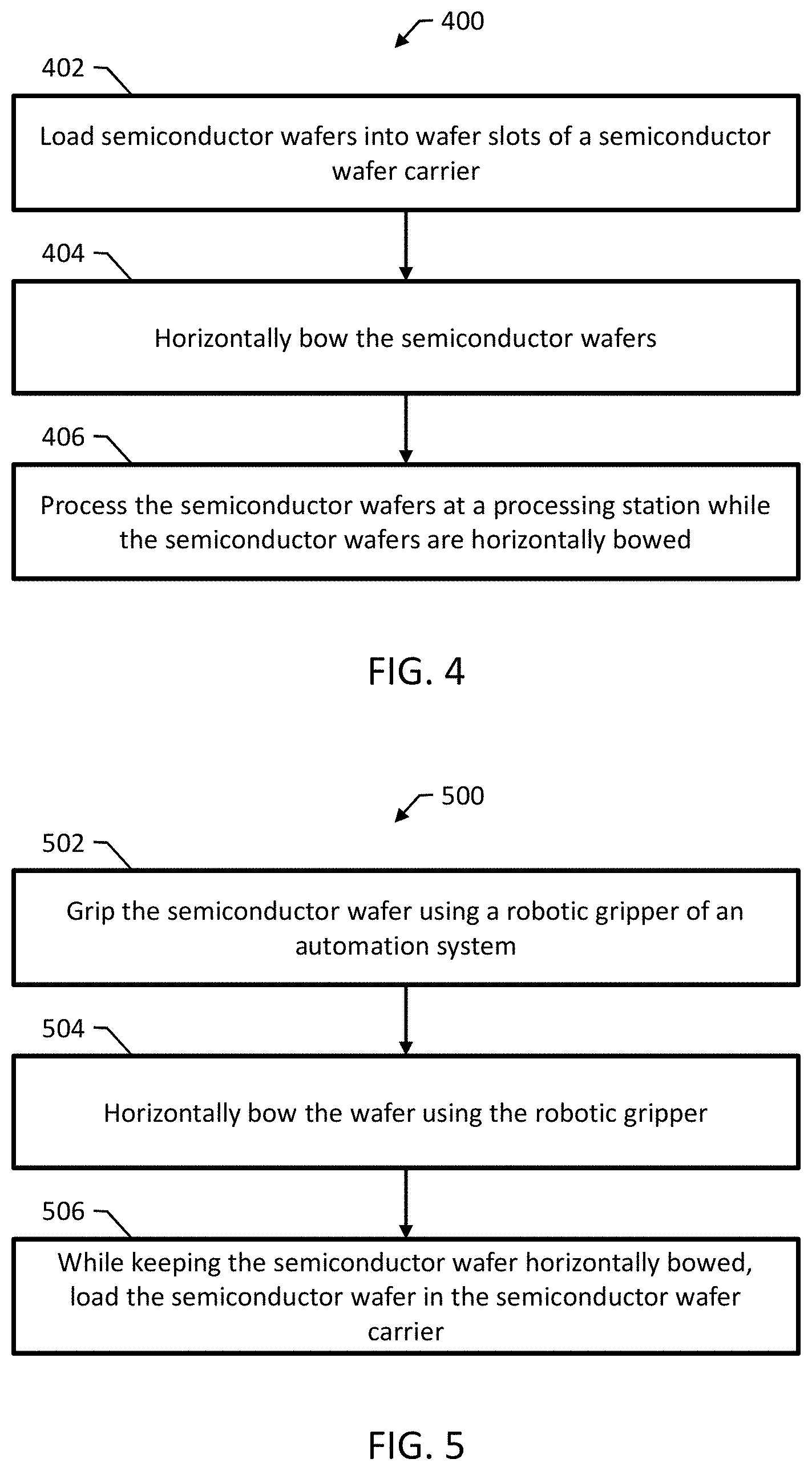
FIG. 4 is a flow diagram of an example method for processing semiconductor wafers; and
FIG. 5 is a flow diagram of an example method for loading semiconductor wafers into a semiconductor wafer carrier.
DETAILED DESCRIPTION
This specification describes methods for processing semiconductor wafers, methods for loading semiconductor wafers into wafer carriers, and semiconductor wafer carriers. The methods and wafer carriers can be used for increasing the rigidity of wafers, e.g., large and thin wafers, by intentionally bowing the wafers to an extent that does not break the wafers. The wafers can be bowed after loading, i.e., within the wafer carrier, or prior to loading, i.e., so that the wafers are loaded so that the remain bowed when loaded. In some examples, the wafers are partially loaded, then bowed, and then fully inserted. In some examples, a method for processing semiconductor wafers includes loading each semiconductor wafer into a respective semiconductor wafer slot of a semiconductor wafer carrier, horizontally bowing each semiconductor wafer, and moving the semiconductor wafer carrier into a processing station and processing the semiconductor wafers at the processing station while the semiconductor wafers are loaded into the semiconductor wafer carrier and horizontally bowed.
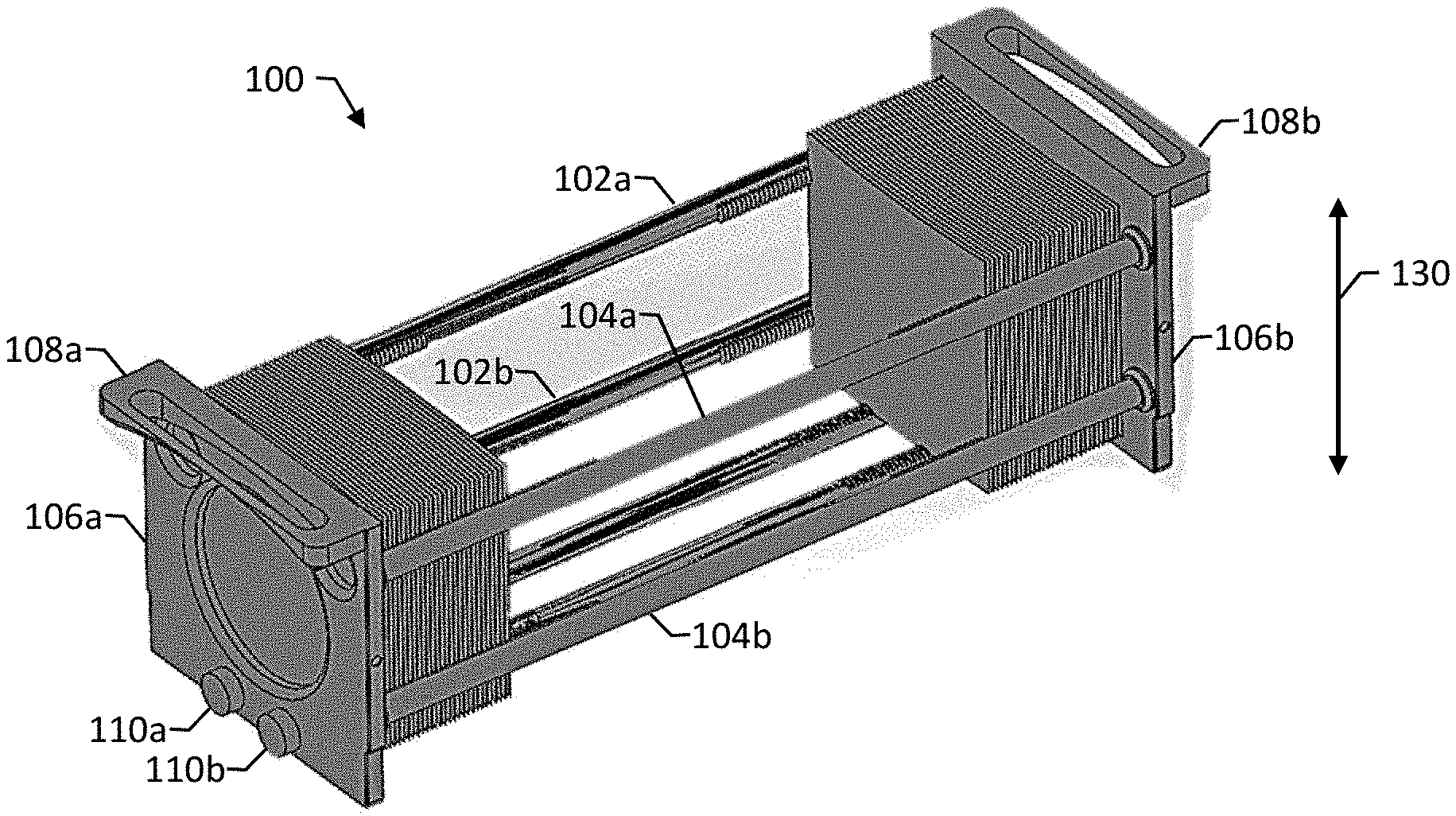
FIGS. 1A-B illustrate an example semiconductor wafer carrier 100. FIG. 1A shows an isometric view of the wafer carrier. FIG. 1B shows a top view of a portion of the wafer carrier 100.
The wafer carrier 100 includes upper and lower left-side rods 102a-b that are parallel in a vertical direction 130. The upper and lower left-side rods 102a-b each have a number of left-side notches. The left-side notches of the upper left-side rod 102a are vertically aligned with the left-side notches of the lower left-side rod 102b. The wafer carrier 100 also includes upper and lower right-side rods 104a-b that are parallel in the vertical direction 130 and have right-side notches that mirror the left-side notches.
Although the wafer carrier 100 is illustrated with upper and lower side rods, in some examples, the wafer carrier 100 has only a single left-side rod and a single right-side rod. Similarly, in some examples, the wafer carrier 100 has more than two side rods on each side that are parallel in the vertical direction 130.
The wafer carrier 100 includes left and right bottom rods 112a-b. Although two bottom rods are illustrated, the wafer carrier 100 can be implemented using only one bottom rod or more than two bottom rods. The left and right bottom rods 112a-b each have a number of bottom notches. The upper and lower left-side rods 102a-b, the upper and lower right-side rods 104a-b, and the bottom rods 112a-b are joined so that the left-side notches face the right-side notches and are horizontally aligned with the bottom-side notches. The notches define a number of semiconductor wafer slots between horizontally-aligned left-side notches, right-side notches, and bottom notches.
For example, each of the semiconductor wafer slots can have a height between the upper left-side and upper right-side rods 102a and 104a and the bottom rods 112a-b sized to receive a standard-conforming polycrystalline solar wafer, for example, a 5 inch or 6 inch wafer (e.g., having a diagonal width across the face of the wafer of 5 inches or 6 inches). Each of the semiconductor wafer slots can have a lateral length between the upper and lower left-side rods 102a-b and the upper and lower right-side rods 104a-b sized to receive the standard-conforming polycrystalline solar wafer.
The upper and lower left-side rods 102a-b, the upper and lower right-side rods 104a-b, and the bottom rods 114a-b may be formed of any appropriate material. Typically, the material is nonreactive two one or more semiconductor manufacturing processes, e.g., chemical processes. For example, the upper and lower left-side rods 102a-b, the upper and lower right-side rods 106a-b, and the bottom rods 110a-b may be formed of quartz or silicon carbide.
In some examples, the wafer carrier 100 includes front and back plates 106a-b. Each of the front and back plates 106a-b extends laterally (in a lateral direction 140) between the upper and lower left-side rods 102a-b and the upper and lower right-side rods 104a-b. The upper and lower left-side rods 102a-b and the upper and lower right-side rods 104a-b and the bottom rods 112a-b are joined by the front and back plates 120a-b to extend horizontally from the front plate 106a to the back plate 106b. The bottom rods 112a-b can be joined to the front and back plates 106a-b at respective hermetically-sealed moving joints.
The wafer carrier includes a mechanical rod-slider 110a-b coupled to the bottom rods 112a-b. The mechanical rod-slider is configured for sliding, in a horizontal direction 120, the bottom rods 112a-b relative to the left and right rods 102a-b and 104a-b. Since the semiconductor wafers are engaged with the notches on the left and right rods 102a-b and 104a-b, the sliding of the bottom rods 112a-b causes horizontal bowing of the semiconductor wafers loaded into the semiconductor wafer slots.
For example, the mechanical rod-slider 110a-b can be a rotatable knob coupled to a leadscrew. In another example, the mechanical rod-slider 110a-b can be a push-and-pull knob coupled to a linear motion stage, or an electrically-controlled linear actuator. If the wafer carrier 100 has more than one bottom rod, the mechanical rod-slider 110a-b can be configured to move all the rods together so that the wafer bows uniformly.
Bowing the wafers can be useful, e.g., to allow high density wafer loading even with wafers that are large and thin. Bowing the wafers can, in some cases, increase the throughput of some processing steps without increasing a physical foot print. In some examples, process parameters such as nozzle pressure and pump flowrate can be adjusted or increased without breaking wafers since the wafers are bowed. Bowing the wafers can reduce or eliminate cross-slotting and improve uniformity by improving position control.
In some examples, the wafer carrier 100 includes front and back transport interface handles 108a-b. The transport interface handles 108a-b can be detachably coupled to the front and back plates 106a-b. The transport interface handles 108a-b can used, e.g., so that an automation system can lift and move the wafer carrier 100.
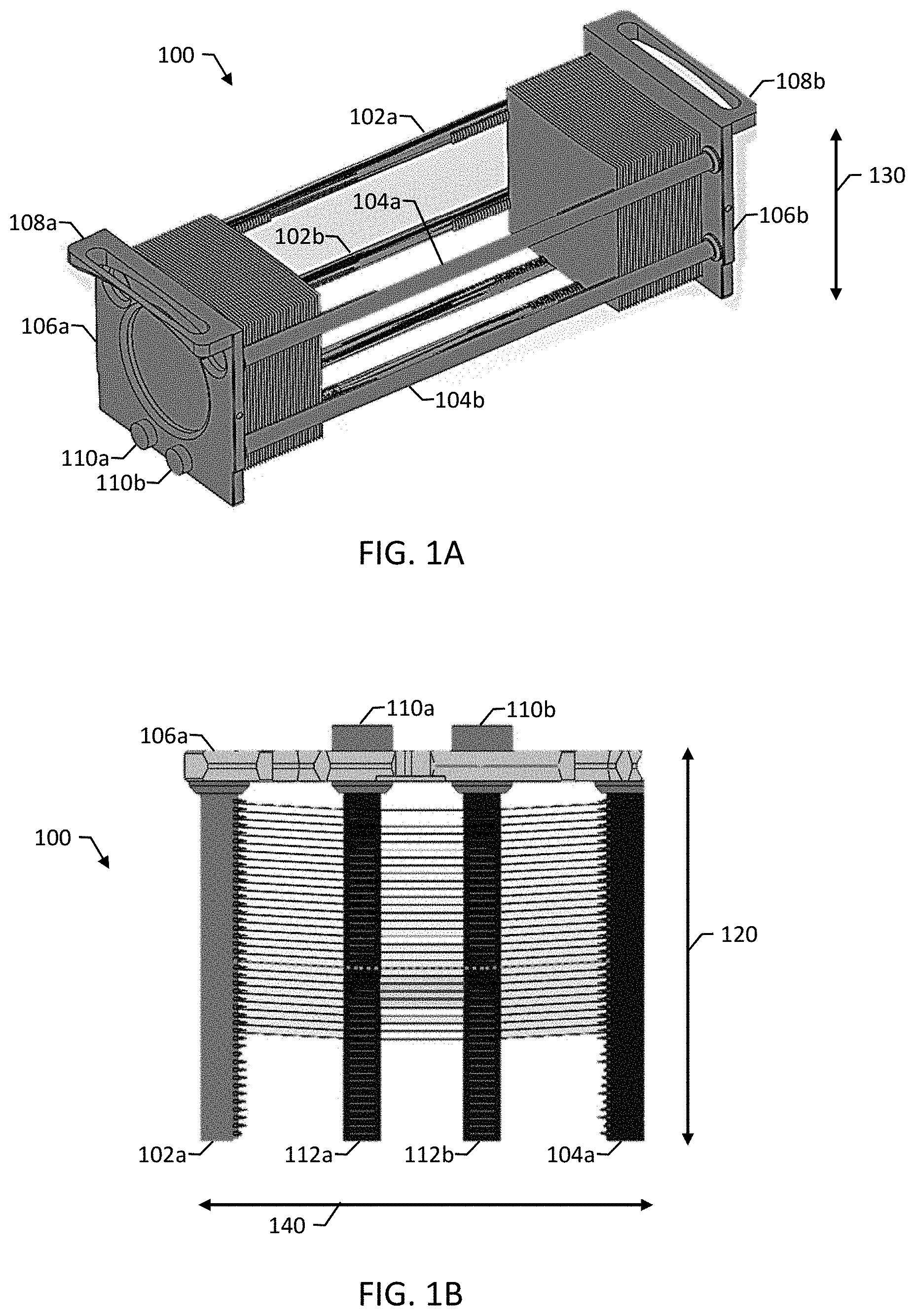
FIGS. 2A-B illustrate a portion of an example automation system 200 for bowing semiconductor wafers prior to loading the wafers into a wafer carrier. The automation system 200 is implemented using robotic components and can be controlled, e.g., by a computer system programmed for loading and processing semiconductor wafers. In general, any appropriate robotic system can be used for bowing the wafers, and the automation system 200 shown in FIGS. 2A-B is provided for purposes of illustration.
The automation system 200 includes a robotic gripper 202 having left and right pistons 204a-b. The robotic gripper 202 is configured to grip a semiconductor wafer 206 and hold the center of the wafer 206 in place. The left and right pistons 204a-b are configured to engage the left and right sides of the wafer 206 and push the wafer 206 to bow without breaking the wafer 206. FIG. 2A shows the robotic gripper 202 holding the wafer 206 prior to bowing the wafer 206. FIG. 2B shows the pistons 204a-b causing the wafer 206 to horizontally bow.
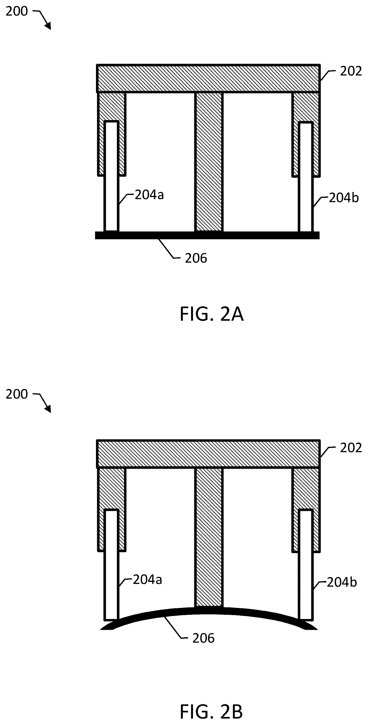
FIGS. 3A-F illustrate loading of a horizontally-bowed semiconductor wafer 308 into an example wafer carrier 300. The wafer carrier 300 includes a left-side rod 302a, a right-side rod 302b, and a bottom rod 304. FIGS. 3A-B illustrate pre-bowing the semiconductor wafer 308 prior to loading, and FIGS. 3C-D illustrate partially loading the semiconductor wafer 308 before bowing the semiconductor wafer 308 and then fully loading the horizontally-bowed semiconductor wafer 308.
FIG. 3A is a top view of the wafer carrier 300 prior to loading of the horizontally-bowed wafer 308 shown in FIG. 3B. The illustrated portion of the wafer carrier 300 has five wafer slots 306a-e each comprising horizontally aligned notches in the left and right rods 302a-b and the bottom rod 304.
FIG. 3B is a top view of the wafer carrier 300 after loading the horizontally-bowed wafer 308. Since the wafer 308 is bowed, the center of the wafer 308 engages the bottom rod 304 in the first wafer slot 306a and the right and left sides of the wafer 308 engage the right and left rods 302a-b in the second wafer slot 306b. For example, the left and right sides of the wafer 308 may be horizontally offset from the center of the wafer 308 by a horizontal distance of about 8 mm, or any appropriate distance that increases the rigidity of the wafer 308 without breaking the wafer 308.
Accordingly, the bottom notch is horizontally offset from the left and right notches, and the wafer carrier 300 keeps the wafer 308 horizontally bowed after the wafer 308 has been bowed and loaded by an automation system such as the example automation system 200 of FIGS. 2A-B. As illustrated, the bottom notch is only offset by one position; however, depending on the distance that the wafer is bowed, the bottom notch may be offset by more than one position from the left and right notches.
FIG. 3C is a top view of the wafer carrier 300 where the wafer 308 has been partially inserted. The wafer 308 has been inserted in the wafer carrier 300 to a first depth so that the right and left sides of the wafer 308 engage the right and left rods 302a-b in the second wafer slot 306b, but the bottom of the wafer 308 has not yet engaged the bottom rod 304. FIG. 3E is a front view of the wafer carrier 300 where the wafer 308 has been partially inserted to the first depth 310a.
FIG. 3D is a top view of the wafer carrier 300 after the wafer 308 has been horizontally bowed and fully inserted to a second depth, deeper than the first depth, so that the bottom of the wafer 308 engages the bottom rod 304 in a bottom notch horizontally offset from the second wafer slot 306b, i.e., the bottom notch for the first wafer slot 306a. FIG. 3F is a front view of the wafer carrier 300 where the wafer 308 has been fully inserted to the second depth 310b.
FIG. 4 is a flow diagram of an example method 400 for processing semiconductor wafers. The method 400 can be performed, e.g., by an automation system for processing semiconductor wafers, or by an automation system acting together with one or more human operators.
The method 400 includes loading each semiconductor wafer into a respective semiconductor wafer slot of a semiconductor wafer carrier (402). The wafer carrier can be, e.g., the wafer carrier 100 of FIGS. 1A and 1B. The method 400 includes horizontally bowing each semiconductor wafer (404). For example, horizontally bowing the wafers can include sliding, in the horizontal direction, one or more bottom rods relative to the left and right rods. The method 400 includes moving the semiconductor wafer carrier into a processing station and processing the semiconductor wafers at the processing station while the semiconductor wafers are loaded into the semiconductor wafer carrier and horizontally bowed (406).
FIG. 5 is a flow diagram of an example method 500 for loading semiconductor wafers into a semiconductor wafer carrier. The method 500 can be performed, e.g., by an automation system for processing semiconductor wafers, or by an automation system acting together with one or more human operators. The wafer carrier can be, e.g., the wafer carrier 300 of FIGS. 3A-B.
The method 500 includes, for each wafer, gripping the wafer using a robotic gripper of an automation system (502). For example, the automation system can be the automation system 200 of FIGS. 2A-B. The method 500 includes, for each wafer, horizontally bowing the wafer using gripper (504). The method 500 includes, for each wafer and while keeping the wafer horizontally bowed, loading the wafer in the semiconductor wafer carrier (506). The wafer sits in horizontally aligned left and right notches in left and right rods of the semiconductor wafer carrier. Due to the horizontal bowing, the wafer sits in at least one bottom notch in a bottom rod that is horizontally offset from the left and right notches in the left and right rods.
Although specific examples and features have been described above, these examples and features are not intended to limit the scope of the present disclosure, even where only a single example is described with respect to a particular feature. Examples of features provided in the disclosure are intended to be illustrative rather than restrictive unless stated otherwise. The above description is intended to cover such alternatives, modifications, and equivalents as would be apparent to a person skilled in the art having the benefit of this disclosure.
The scope of the present disclosure includes any feature or combination of features disclosed in this specification (either explicitly or implicitly), or any generalization of features disclosed, whether or not such features or generalizations mitigate any or all of the problems described in this specification. Accordingly, new claims may be formulated during prosecution of this application (or an application claiming priority to this application) to any such combination of features. In particular, with reference to the appended claims, features from dependent claims may be combined with those of the independent claims and features from respective independent claims may be combined in any appropriate manner and not merely in the specific combinations enumerated in the appended claims.
* * * * *
D00000
D00001
D00002
D00003
D00004
D00005
XML
uspto.report is an independent third-party trademark research tool that is not affiliated, endorsed, or sponsored by the United States Patent and Trademark Office (USPTO) or any other governmental organization. The information provided by uspto.report is based on publicly available data at the time of writing and is intended for informational purposes only.
While we strive to provide accurate and up-to-date information, we do not guarantee the accuracy, completeness, reliability, or suitability of the information displayed on this site. The use of this site is at your own risk. Any reliance you place on such information is therefore strictly at your own risk.
All official trademark data, including owner information, should be verified by visiting the official USPTO website at www.uspto.gov. This site is not intended to replace professional legal advice and should not be used as a substitute for consulting with a legal professional who is knowledgeable about trademark law.