Shared bit line array architecture for magnetoresistive memory
Hoang , et al.
U.S. patent number 10,679,685 [Application Number 15/855,660] was granted by the patent office on 2020-06-09 for shared bit line array architecture for magnetoresistive memory. This patent grant is currently assigned to Spin Memory, Inc.. The grantee listed for this patent is SPIN MEMORY, Inc.. Invention is credited to Loc Hoang, Amitay Levi.

| United States Patent | 10,679,685 |
| Hoang , et al. | June 9, 2020 |
Shared bit line array architecture for magnetoresistive memory
Abstract
A magnetoresistive memory architecture in one aspect includes a plurality of bit lines each coupled to two or more respective columns of magnetoresistive memory cells, and a plurality of source lines each coupled to a respective one of the columns of memory cells. A given memory cell can be accessed by biasing a selected word line, a selected bit line, and a selected source line coupled to corresponding column of memory cells coupled to the selected bit line, and by counter biasing one or more selected source lines coupled to one or more other columns of memory cells coupled to the selected bit line.
| Inventors: | Hoang; Loc (Fremont, CA), Levi; Amitay (Fremont, CA) | ||||||||||
|---|---|---|---|---|---|---|---|---|---|---|---|
| Applicant: |
|
||||||||||
| Assignee: | Spin Memory, Inc. (Fremont,
CA) |
||||||||||
| Family ID: | 66951355 | ||||||||||
| Appl. No.: | 15/855,660 | ||||||||||
| Filed: | December 27, 2017 |
Prior Publication Data
| Document Identifier | Publication Date | |
|---|---|---|
| US 20190198078 A1 | Jun 27, 2019 | |
| Current U.S. Class: | 1/1 |
| Current CPC Class: | G11C 11/161 (20130101); G11C 11/1653 (20130101); G11C 11/1659 (20130101); G11C 11/1657 (20130101); G11C 11/1675 (20130101); H01L 27/228 (20130101); H01L 43/02 (20130101); G11C 11/1655 (20130101); G11C 11/1673 (20130101); G11C 2213/82 (20130101); G11C 2213/79 (20130101) |
| Current International Class: | G11C 11/16 (20060101); H01L 27/22 (20060101); H01L 43/02 (20060101) |
| Field of Search: | ;365/158 |
References Cited [Referenced By]
U.S. Patent Documents
| 5541868 | July 1996 | Prinz |
| 5629549 | May 1997 | Johnson |
| 5640343 | June 1997 | Gallagher et al. |
| 5654566 | August 1997 | Johnson |
| 5691936 | November 1997 | Sakakima et al. |
| 5695846 | December 1997 | Lange et al. |
| 5695864 | December 1997 | Slonczewski |
| 5732016 | March 1998 | Chen et al. |
| 5856897 | January 1999 | Mauri |
| 5896252 | April 1999 | Kanai |
| 5966323 | October 1999 | Chen et al. |
| 6016269 | January 2000 | Peterson et al. |
| 6055179 | April 2000 | Koganei et al. |
| 6097579 | August 2000 | Gill |
| 6124711 | September 2000 | Tanaka et al. |
| 6134138 | October 2000 | Lu et al. |
| 6140838 | October 2000 | Johnson |
| 6154139 | November 2000 | Kanai et al. |
| 6172902 | January 2001 | Wegrowe et al. |
| 6233172 | May 2001 | Chen et al. |
| 6243288 | June 2001 | Ishikawa et al. |
| 6252798 | June 2001 | Satoh et al. |
| 6256223 | July 2001 | Sun |
| 6292389 | September 2001 | Chen et al. |
| 6347049 | February 2002 | Childress et al. |
| 6376260 | April 2002 | Chen et al. |
| 6385082 | May 2002 | Abraham et al. |
| 6436526 | August 2002 | Odagawa et al. |
| 6458603 | October 2002 | Kersch et al. |
| 6493197 | December 2002 | Ito et al. |
| 6522137 | February 2003 | Sun et al. |
| 6532164 | March 2003 | Redon et al. |
| 6538918 | March 2003 | Swanson et al. |
| 6545906 | April 2003 | Savtchenko et al. |
| 6563681 | May 2003 | Sasaki et al. |
| 6566246 | May 2003 | deFelipe et al. |
| 6603677 | August 2003 | Redon et al. |
| 6653153 | November 2003 | Doan et al. |
| 6654278 | November 2003 | Engel et al. |
| 6677165 | January 2004 | Lu et al. |
| 6710984 | March 2004 | Yuasa et al. |
| 6713195 | March 2004 | Wang et al. |
| 6714444 | March 2004 | Huai et al. |
| 6744086 | June 2004 | Daughton et al. |
| 6750491 | June 2004 | Sharma et al. |
| 6765824 | July 2004 | Kishi et al. |
| 6772036 | August 2004 | Eryurek et al. |
| 6773515 | August 2004 | Li et al. |
| 6777730 | August 2004 | Daughton et al. |
| 6812437 | November 2004 | Levy et al. |
| 6829161 | December 2004 | Huai et al. |
| 6835423 | December 2004 | Chen et al. |
| 6838740 | January 2005 | Huai et al. |
| 6842317 | January 2005 | Sugita et al. |
| 6847547 | January 2005 | Albert et al. |
| 6887719 | May 2005 | Lu et al. |
| 6888742 | May 2005 | Nguyen et al. |
| 6902807 | June 2005 | Argoitia et al. |
| 6906369 | June 2005 | Ross et al. |
| 6920063 | July 2005 | Huai et al. |
| 6933155 | August 2005 | Albert et al. |
| 6958927 | October 2005 | Nguyen et al. |
| 6967863 | November 2005 | Huai |
| 6980469 | December 2005 | Kent et al. |
| 6985385 | January 2006 | Nguyen et al. |
| 6992359 | January 2006 | Nguyen et al. |
| 6995962 | February 2006 | Saito et al. |
| 7002839 | February 2006 | Kawabata et al. |
| 7005958 | February 2006 | Wan |
| 7006375 | February 2006 | Covington |
| 7009877 | March 2006 | Huai et al. |
| 7041598 | May 2006 | Sharma |
| 7045368 | May 2006 | Hong et al. |
| 7170778 | January 2007 | Kent et al. |
| 7190611 | March 2007 | Nguyen et al. |
| 7203129 | April 2007 | Lin et al. |
| 7227773 | June 2007 | Nguyen et al. |
| 7262941 | August 2007 | Li et al. |
| 7307876 | December 2007 | Kent et al. |
| 7335960 | February 2008 | Han et al. |
| 7351594 | April 2008 | Bae et al. |
| 7352021 | April 2008 | Bae et al. |
| 7376006 | May 2008 | Bednorz et al. |
| 7449345 | November 2008 | Horng et al. |
| 7476919 | January 2009 | Hong et al. |
| 7573737 | August 2009 | Kent et al. |
| 7619431 | November 2009 | DeWilde et al. |
| 7911832 | March 2011 | Kent et al. |
| 7936595 | May 2011 | Han et al. |
| 7986544 | July 2011 | Kent et al. |
| 8279666 | October 2012 | Dieny et al. |
| 8334213 | December 2012 | Mao |
| 8363465 | January 2013 | Kent et al. |
| 8492881 | July 2013 | Kuroiwa et al. |
| 8535952 | September 2013 | Ranjan et al. |
| 8574928 | November 2013 | Satoh et al. |
| 8617408 | December 2013 | Balamane |
| 8716817 | May 2014 | Saida |
| 8737137 | May 2014 | Choy et al. |
| 9025367 | May 2015 | Lin |
| 9082888 | July 2015 | Kent et al. |
| 9263667 | February 2016 | Pinarbasi |
| 9406876 | August 2016 | Pinarbasi |
| 9583166 | February 2017 | Gharia |
| 9853206 | December 2017 | Pinarbasi |
| 10163479 | December 2018 | Berger |
| 2002/0090533 | July 2002 | Zhang et al. |
| 2002/0105823 | August 2002 | Redon et al. |
| 2003/0117840 | June 2003 | Sharma et al. |
| 2003/0151944 | August 2003 | Saito |
| 2003/0197984 | October 2003 | Inomata et al. |
| 2003/0218903 | November 2003 | Luo |
| 2004/0012994 | January 2004 | Slaughter et al. |
| 2004/0061154 | April 2004 | Huai et al. |
| 2004/0094785 | May 2004 | Zhu et al. |
| 2004/0130936 | July 2004 | Nguyen et al. |
| 2004/0257717 | December 2004 | Sharma et al. |
| 2005/0041342 | February 2005 | Huai et al. |
| 2005/0051820 | March 2005 | Stojakovic et al. |
| 2005/0063222 | March 2005 | Huai et al. |
| 2005/0104101 | May 2005 | Sun et al. |
| 2005/0128842 | June 2005 | Wei |
| 2005/0136600 | June 2005 | Huai |
| 2005/0158881 | July 2005 | Sharma |
| 2005/0180202 | August 2005 | Huai et al. |
| 2005/0184839 | August 2005 | Nguyen et al. |
| 2005/0201023 | September 2005 | Huai et al. |
| 2005/0237787 | October 2005 | Huai et al. |
| 2005/0280058 | December 2005 | Pakala et al. |
| 2006/0018057 | January 2006 | Huai |
| 2006/0049472 | March 2006 | Diao et al. |
| 2006/0087880 | April 2006 | Mancoff et al. |
| 2006/0092696 | May 2006 | Bessho |
| 2006/0132990 | June 2006 | Morise et al. |
| 2006/0227465 | October 2006 | Inokuchi et al. |
| 2007/0019337 | January 2007 | Apalkov et al. |
| 2007/0242501 | October 2007 | Hung et al. |
| 2008/0043514 | February 2008 | Ueda |
| 2008/0049488 | February 2008 | Rizzo |
| 2008/0112094 | May 2008 | Kent et al. |
| 2008/0151614 | June 2008 | Guo |
| 2008/0259508 | October 2008 | Kent et al. |
| 2008/0297292 | December 2008 | Viala et al. |
| 2009/0046501 | February 2009 | Ranjan et al. |
| 2009/0072185 | March 2009 | Raksha et al. |
| 2009/0091037 | April 2009 | Assefa et al. |
| 2009/0098413 | April 2009 | Kanegae |
| 2009/0161421 | June 2009 | Cho et al. |
| 2009/0209102 | August 2009 | Zhong et al. |
| 2009/0231909 | September 2009 | Dieny et al. |
| 2010/0124091 | May 2010 | Cowburn |
| 2010/0193891 | August 2010 | Wang et al. |
| 2010/0246254 | September 2010 | Prejbeanu et al. |
| 2010/0271870 | October 2010 | Zheng et al. |
| 2010/0290275 | November 2010 | Park et al. |
| 2011/0032645 | February 2011 | Noel et al. |
| 2011/0058412 | March 2011 | Zheng et al. |
| 2011/0089511 | April 2011 | Keshtbod et al. |
| 2011/0133298 | June 2011 | Chen et al. |
| 2012/0052258 | March 2012 | Op DeBeeck et al. |
| 2012/0069649 | March 2012 | Ranjan et al. |
| 2012/0280336 | June 2012 | Watts |
| 2012/0181642 | July 2012 | Prejbeanu et al. |
| 2012/0188818 | July 2012 | Ranjan et al. |
| 2012/0280339 | November 2012 | Zhang et al. |
| 2012/0294078 | November 2012 | Kent et al. |
| 2012/0299133 | November 2012 | Son et al. |
| 2013/0001506 | January 2013 | Sato et al. |
| 2013/0001652 | January 2013 | Yoshikawa et al. |
| 2013/0021841 | January 2013 | Zhou et al. |
| 2013/0244344 | September 2013 | Malmhall et al. |
| 2013/0267042 | October 2013 | Satoh et al. |
| 2013/0270661 | October 2013 | Yi et al. |
| 2013/0307097 | November 2013 | Yi et al. |
| 2013/0341801 | December 2013 | Satoh et al. |
| 2014/0009994 | January 2014 | Parkin et al. |
| 2014/0042571 | February 2014 | Gan et al. |
| 2014/0070341 | March 2014 | Beach et al. |
| 2014/0103472 | April 2014 | Kent et al. |
| 2014/0169085 | June 2014 | Wang et al. |
| 2014/0177316 | June 2014 | Otsuka et al. |
| 2014/0217531 | August 2014 | Jan |
| 2014/0252439 | September 2014 | Guo |
| 2014/0264671 | September 2014 | Chepulskyy et al. |
| 2014/0340958 | November 2014 | Gharia |
| 2015/0056368 | February 2015 | Wang et al. |
| 2016/0087193 | March 2016 | Pinarbasi et al. |
| 2016/0163973 | June 2016 | Pinarbasi |
| 2016/0372518 | December 2016 | Li |
| 2016/0372656 | December 2016 | Pinarbasi |
| 2017/0047107 | February 2017 | Berger |
| 2766141 | Jan 2011 | CA | |||
| 105706259 | Jun 2016 | CN | |||
| 1345277 | Sep 2003 | EP | |||
| 2817998 | Jun 2002 | FR | |||
| 2832542 | May 2003 | FR | |||
| 2910716 | Jun 2008 | FR | |||
| H10-004012 | Jan 1998 | JP | |||
| H11-120758 | Apr 1999 | JP | |||
| H11-352867 | Dec 1999 | JP | |||
| 2001-195878 | Jul 2001 | JP | |||
| 2002-261352 | Sep 2002 | JP | |||
| 2002-357489 | Dec 2002 | JP | |||
| 2003-318461 | Nov 2003 | JP | |||
| 2005-044848 | Feb 2005 | JP | |||
| 2005-150482 | Jun 2005 | JP | |||
| 2005-535111 | Nov 2005 | JP | |||
| 2006128579 | May 2006 | JP | |||
| 2008-524830 | Jul 2008 | JP | |||
| 2009-027177 | Feb 2009 | JP | |||
| 2013-012546 | Jan 2013 | JP | |||
| 2014-039061 | Feb 2014 | JP | |||
| 5635666 | Dec 2014 | JP | |||
| 2015-002352 | Jan 2015 | JP | |||
| 10-2014-015246 | Sep 2014 | KR | |||
| 2009-080636 | Jul 2009 | WO | |||
| 2011-005484 | Jan 2011 | WO | |||
| 2014-062681 | Apr 2014 | WO | |||
Claims
What is claimed is:
1. A memory device comprising: a plurality of memory cells arranged in a plurality of rows and a plurality of columns, wherein each memory cell includes a Magnetic Tunneling Junction (MTJ) and a transistor, wherein a drain of the transistor is coupled to a first terminal of the MJT; a plurality of bit lines, wherein each bit line is coupled to a second terminal of the MTJs of the memory cells in two or more respective columns of the memory cells; a plurality of source lines, wherein each source line is coupled to a source of the transistors of the memory cells in a respective column of the memory cells; a plurality of word lines, wherein each word line is coupled to a gate of the transistors of the memory cells in a respective row of the memory cells; and a control circuit configured to apply corresponding biases to a select word line, the plurality of bit lines and the plurality source lines to write data in parallel to cells in the select word line, including biases to a select bit line and a select source line coupled to the select hit line, and to apply a corresponding counter bias to one or more other source lines coupled to the select bit line to write a given value to a given memory cell.
2. The memory device of claim 1, wherein the control circuit is further configured to: apply a word line write voltage to the select word line; apply a bit line write voltage to the select hit line; apply a ground voltage to the select source line; apply the bit line write voltage to the one or more other source lines coupled to the select bit line; and wherein a `0` state is written to the given memory cell.
3. The memory device of claim 2, wherein the control circuit is further configured to: apply a word line write voltage to the select word line; apply a ground voltage to the select bit hue; apply a source line write voltage to the select source line; apply the ground voltage to the one or more other source lines coupled to the select bit line; and wherein a `1` state is written to the given memory cell.
4. The memory device of claim 1, wherein the control circuit is further configured to apply corresponding biases to the select word line, the select bit line and the select source line coupled to the select bit line, and to apply a corresponding counter bias to one or more other source lines coupled to the select bit line to read the given memory cell from the select bit line.
5. The memory device of claim 4, wherein the control circuit is further configured to: apply a word line read voltage to the select word line; apply a bit line read voltage to the select bit line; apply a ground voltage to the select source line; and apply the bit line read voltage to the one or more other source lines coupled to the select bit line.
6. The memory device of claim 1, wherein the control circuit is further configured to: apply a word line read voltage to the select word line; apply aground voltage to the select bit line; apply a source line read voltage to the select source line; apply the ground voltage to the one or more other source lines coupled to the select bit line; and wherein the given memory cell is read from the select bit line.
7. The memory device according to claim 1, wherein the plurality of memory cells comprise, a plurality of spin torque magnetoresistive memory cells.
8. The memory device according, to claim 1, wherein the plurality of bit lines and the plurality of source lines are substantially parallel to each other; and the plurality of word lines are substantially parallel to each other and substantially perpendicular to the plurality of bit lines and the plurality of source lines.
9. A Magnetoresistive Random-Access Memory (MRAM) comprising: a memory cell array including; a plurality of magnetoresistive memory cells arranged in a plurality of columns and rows; a plurality of word lines, wherein each word line is coupled to a corresponding row of the magnetoresistive memory cells; a plurality of bit lines, wherein each bit line is coupled to a first one and a second one of a pair of columns of the magnetoresistive memory cells; and a plurality of pairs of source lines, wherein a first one of each pair of source lines is coupled to corresponding first ones of the pair of columns of the magnetoresistive memory cells and a second one of each pair source lines is coupled to corresponding second ones of the pair of columns of the magnetoresistive memory cells; and a control circuit coupled to memory cell array, wherein the control circuit is configured bias a select word line, bias the plurality of bit lines, bias the first ones of the pairs of source lines and counter bias the second one of the pairs of source line relative to the first one of the pairs of source lines to access magnetoresistive memory cell in the select word line.
10. The MRAM of claim 9, wherein the control circuit is further configured to: bias the select word line at a word line write voltage; bias a given one of the bit lines at a bit line write voltage; bias a corresponding one of the first source lines at a ground voltage; and bias a corresponding one of the second source lines at the bit line write voltage, wherein a `0` state is written to a given memory cell.
11. The MRAM of claim 10, wherein the control circuit is further configured to: bias the select word line at a word line write voltage; bias a given one of the bit line at a ground voltage; bias a corresponding one of the first source lines at a source line write voltage; and bias a corresponding one of the second source lines at the ground voltage, wherein a `1` state is written to the given memory cell.
12. The MRAM of claim 9, wherein the control circuit is further configured to: bias the select word line at a word line read voltage; bias a given one of the bit line a bit line read voltage; bias a corresponding one of the first source lines at a ground voltage; and bias a corresponding one of the second source lines at the bit line read voltage, wherein a state of a given memory cell is read from the corresponding one of first source line.
13. The MRAM of claim 9, wherein the control circuit is further configured to: bias the select word line at a word line read voltage; bias a given one of the bit line a ground voltage; bias a corresponding one of the first source lines at a source line read voltage; and bias a corresponding one of the second source lines at the ground voltage, wherein at state of the given memory cell is read from the bit line.
14. The MRAM according to claim 9, wherein the plurality of magnetoresistive memory cells comprise, a plurality of spin torque magnetoresistive memory cells.
15. The MRAM according to claim 14, wherein the plurality of spin torque magnetoresistive memory cells each comprise, a pillar including: one or more seed layers; one or more synthetic antiferromagnetic layers; one or more reference magnetic layers; one or more magnetic tunneling barrier layers; one or more free magnetic layers; one or more non-magnetic spacer layers; one or more perpendicular polarizer layers; one or more capping layers; and one or more hard mask layers.
16. A method of accessing a Magnetoresistive Random-Access Memory (MRAM) comprising: biasing a selected word line coupled to a row of a plurality of Magnetic Tunnel Junction (MTJ) memory cells including a given MTJ memory cell; biasing a plurality of bit lines in parallel, including biasing a selected bit line coupled to a first and a second column of the plurality of MTJ memory cells, wherein the first column of the plurality of MTJ memory cells, includes the given MTJ memory cell; and biasing a plurality of source lines in parallel, including a bias of a selected source line coupled to the first column of the plurality of MTJ memory cells including the given MTJ memory cell, and a counter bias of a selected source line coupled to the second column of the plurality of MTJ memory cells.
17. The method of accessing the MRAM of claim 16, including writing a `0` state to the given MTJ memory cell comprising: applying a word line write voltage to the selected word line coupled to the row of MTJ memory cells including the given MTJ memory cell; applying a bit line write voltage to, the selected lit line coupled to the first and the second columns of the plurality of MTJ memory cells; applying a ground voltage to the selected source line coupled to the first column of the plurality of MTJ memory cells including the given MTJ memory cell; and applying the bit line write voltage to the selected source line coupled to the second column of the plurality of MTJ memory cells.
18. The method of accessing the MRAM of claim 17, including writing a `1` state to the given MTJ memory cell comprising: applying the word line write voltage to the selected word line coupled to the row of MTJ memory cells including the given MTJ memory cell; applying the ground voltage to the selected hit line coupled to the first and the second columns of the plurality of MTJ memory cells; applying a source line write voltage to the selected source line coupled to the first column of the plurality of NM memory cells including the given MTJ memory cell; and applying the ground voltage to the selected source line coupled to the second column of the plurality of MTJ memory cells.
19. The method of accessing the MRAM of claim 18, including reading a current state of the given MTJ memory cell comprising: applying a word line read voltage to the selected word line coupled to the row of the plurality of MD memory cells including the given MTJ memory cell; applying a bit line read voltage to the selected bit line coupled to the first and the second columns of the plurality of MTJ memory cells; applying the ground voltage to the selected source line coupled to the first column of the plurality of MTJ memory cells including the given MTJ memory cell; applying the bit line read voltage to the selected source line coupled to the second column of the plurality of MTJ memory cells; and sensing the selected source line coupled to the first column of the plurality of MTJ memory cells to determine the current state of the given MD memory cell.
20. The method of accessing the MRAM of claim 18, including reading a current state of the given MTJ memory cell comprising: applying a word line read voltage to the selected word line coupled to the row of the plurality of MD memory cells including the given MTJ memory cell; applying the ground voltage to the selected bit line coupled to the first and the second columns of the plurality of MTJ memory cells; applying a source line read voltage to the selected source line coupled to the first column of the plurality of MD memory cells including the given MIST memory cell; applying the ground voltage to the selected source line coupled to the second column of the plurality of MTJ memory cells; and sensing the selected bit line coupled to the first and the second columns of the plurality of MTJ memory cells to determine the current state of the given MTJ memory cell.
Description
BACKGROUND OF THE INVENTION
Computing systems have made significant contributions toward the advancement of modern society and are utilized in a number of applications to achieve advantageous results. Numerous devices, such as desktop personal computers (PCs), laptop PCs, tablet PCs, netbooks, smart phones, game consoles, servers, distributed computing systems, and the like have facilitated increased productivity and reduced costs in communicating and analyzing data in most areas of entertainment, education, business, and science. One common aspect of computing systems is the computing device readable memory. Computing devices may include one or more types of memory, such as volatile random-access memory, non-volatile flash memory, and the like.
An emerging non-volatile memory technology is Magnetoresistive Random Access Memory (MRAM). In MRAM devices, data can be stored in the magnetization orientation between ferromagnetic layers. Typically, if the ferromagnetic layers have the same magnetization polarization, the cell will exhibit a relatively low resistance value corresponding to a `0` bit state; while if the magnetization polarization between the two ferromagnetic layers is antiparallel the memory cell will exhibit a relatively high resistance value corresponding to a `1` bit state. Because the data is stored in the magnetic fields, MRAM devices are non-volatile memory devices. The state of a MRAM cell can be read by applying a predetermined current through the cell and measuring the resulting voltage, or by applying a predetermined voltage across the cell and measuring the resulting current. The sensed current or voltage is proportional to the resistance of the cell and can be compared to a reference value to determine the state of the cell.
MRAM devices are characterized by densities similar to Dynamic Random-Access Memory (DRAM), power consumption similar to flash memory, and speed similar to Static Random-Access Memory (SRAM). However, similar to other memory types, there is a continuing need to achieve further device scaling of MRAM devices and/or reduce device defects.
SUMMARY OF THE INVENTION
The present technology may best be understood by referring to the following description and accompanying drawings that are used to illustrate embodiments of the present technology that are directed toward a shared bit line architecture for magnetoresistive memory.
In one embodiment, a memory device can include a plurality of memory cells, a plurality of bit lines, a plurality of source lines, a plurality of word lines, and a control circuit. The plurality of memory cells can be arranged in a plurality of rows and a plurality of columns. Each memory cell can include a Magnetic Tunneling Junction (MTJ) and a transistor, wherein a drain of the transistor can be coupled to a first terminal of the MTJ. Each bit line can be coupled to a second terminal of the MTJs in two or more respective columns of the memory cells. Each source line can be coupled to a source of the transistors of the memory cells in a respective column of the memory cells. Each word line can be coupled to a gate of the transistors of the memory cells in a respective row of the memory cells. The control circuit can be configured to apply corresponding biases to a select word line, a select bit line and a select source line coupled to the select bit line, and to apply a corresponding counter bias to one or more other source lines coupled to the select bit line to write a given value to a given memory cell.
In another embodiment, a Magnetoresistive Random-Access Memory (MRAM) can include a memory cell array and a control circuit. The memory cell array can include a plurality of magnetoresistive memory cells arranged in a plurality of columns and rows. The memory cell array can also include a plurality of word lines, a plurality of bit lines and a plurality of source lines. In the memory cell array, a word line can be coupled to a row of the magnetoresistive memory cells, a bit line can be coupled to a first and second column of the magnetoresistive memory cells, a first source line can be coupled to the first column of magnetoresistive memory cells, and a second source line can be coupled to the second column magnetoresistive memory cells. The control circuit can be configured to bias the word line, bias the bit lines, bias the first source line and counter bias the second source line to access a given magnetoresistive memory cell.
In one example, the control circuit can bias the word line at a word line write voltage, bias the bit line at a bit line write voltage, bias the first source line at a ground voltage and bias the second source line at the bit line write voltage to write a `0` state to the given memory cell. To write a `1` state to the given memory cell, the control circuit can bias the word line at a word line write voltage, bias the bit line at a ground voltage, bias the first source line at a source line write voltage, and bias the second source line at the ground voltage. In another example, the control circuit can bias the word line at a word line read voltage, bias the bit line a bit line read voltage, bias the first source line at a ground voltage, and bias the second source line at the bit line read voltage to read the state of the given memory cell using the first source line. In yet another example, the control circuit can bias the word line at a word line read voltage, bias the bit line a ground voltage, bias the first source line at a source line read voltage, and bias the second source line at the ground voltage to read the state of the given memory cell using the bit line.
In another embodiment, a method of accessing a MRAM can include biasing a selected word line coupled to a row of a plurality of MTJ memory cells. To access a given MTJ memory cell, the method can also include biasing a selected bit line coupled to a first and second column of the plurality of MTJ memory cells, wherein the first column of the plurality of MTJ memory cells includes the given MTJ memory cell. The method can also include biasing a selected source line coupled to the first column of the plurality of MTJ memory cells including the given MTJ memory cell. The method can also include counter biasing selected source line coupled to the second column of the plurality of MTJ memory cells.
This Summary is provided to introduce a selection of concepts in a simplified form that are further described below in the Detailed Description. This Summary is not intended to identify key features or essential features of the claimed subject matter, nor is it intended to be used to limit the scope of the claimed subject matter.
BRIEF DESCRIPTION OF THE DRAWINGS
Embodiments of the present technology are illustrated by way of example and not by way of limitation, in the figures of the accompanying drawings and in which like reference numerals refer to similar elements and in which:
FIG. 1 shows an isometric representation of a Magnetoresistive Random Access Memory (MRAM) cell array, in accordance with the conventional art.
FIG. 2 shows a circuit diagram of a MRAM cell array, in accordance with the conventional art.
FIG. 3 shows a block diagram of a MRAM, in accordance with embodiments of the present technology.
FIG. 4 shows an isometric representation of a MRAM cell array, in accordance with embodiments of the present technology.
FIG. 5 shows a circuit diagram of a MRAM memory cell array, in accordance with embodiments of the present technology.
DETAILED DESCRIPTION OF THE INVENTION
Reference will now be made in detail to the embodiments of the present technology, examples of which are illustrated in the accompanying drawings. While the present technology will be described in conjunction with these embodiments, it will be understood that they are not intended to limit the invention to these embodiments. On the contrary, the invention is intended to cover alternatives, modifications and equivalents, which may be included within the scope of the invention as defined by the appended claims. Furthermore, in the following detailed description of the present technology, numerous specific details are set forth in order to provide a thorough understanding of the present technology. However, it is understood that the present technology may be practiced without these specific details. In other instances, well-known methods, procedures, components, and circuits have not been described in detail as not to unnecessarily obscure aspects of the present technology.
Some embodiments of the present technology which follow are presented in terms of routines, modules, logic blocks, and other symbolic representations of operations on data within one or more electronic devices. The descriptions and representations are the means used by those skilled in the art to most effectively convey the substance of their work to others skilled in the art. A routine, module, logic block and/or the like, is herein, and generally, conceived to be a self-consistent sequence of processes or instructions leading to a desired result. The processes are those including physical manipulations of physical quantities. Usually, though not necessarily, these physical manipulations take the form of electric or magnetic signals capable of being stored, transferred, compared and otherwise manipulated in an electronic device. For reasons of convenience, and with reference to common usage, these signals are referred to as data, bits, values, elements, symbols, characters, terms, numbers, strings, and/or the like with reference to embodiments of the present technology.
It should be borne in mind, however, that all of these terms are to be interpreted as referencing physical manipulations and quantities and are merely convenient labels and are to be interpreted further in view of terms commonly used in the art. Unless specifically stated otherwise as apparent from the following discussion, it is understood that through discussions of the present technology, discussions utilizing the terms such as "receiving," and/or the like, refer to the actions and processes of an electronic device such as an electronic computing device that manipulates and transforms data. The data is represented as physical (e.g., electronic) quantities within the electronic device's logic circuits, registers, memories and/or the like, and is transformed into other data similarly represented as physical quantities within the electronic device.
In this application, the use of the disjunctive is intended to include the conjunctive. The use of definite or indefinite articles is not intended to indicate cardinality. In particular, a reference to "the" object or "a" object is intended to denote also one of a possible plurality of such objects. It is also to be understood that the phraseology and terminology used herein is for the purpose of description and should not be regarded as limiting.
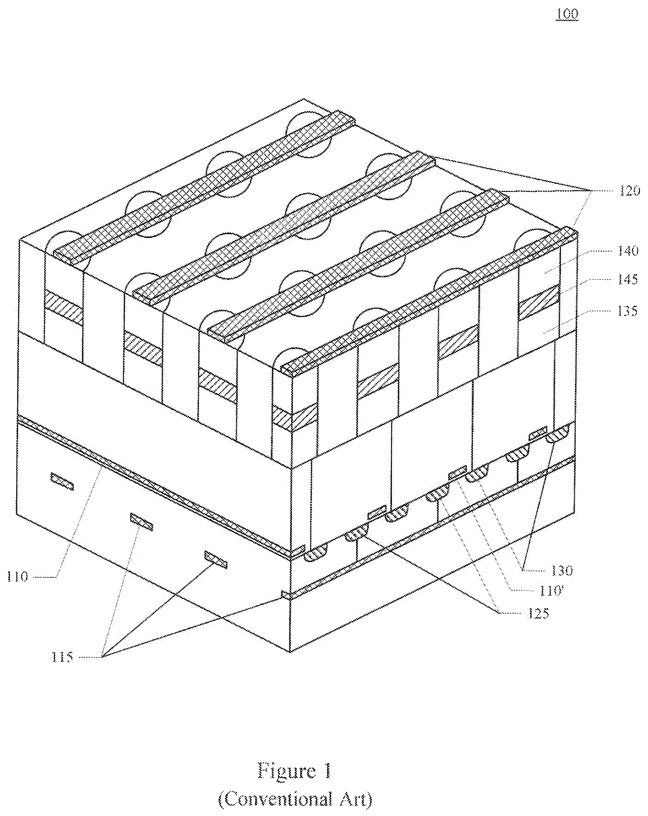
Before describing embodiments of the present technology in detail, a description of conventional MRAM devices is provided for reference. Referring to FIG. 1, an isometric representation of a MRAM cell array, in accordance with the conventional art, is shown. The MRAM cell array 100 can include a plurality of memory cells organized in rows and columns, with sets of word lines 110, source lines 115 and bit lines 120. Each memory cell can include a Magnetic Tunneling Junction (MTJ) and an access transistor arranged in columns and rows. The access transistors can each include a source region 125, a drain region 130, a body region, a gate region 110' and a gate insulator region. The source regions 125 in each column of access transistors can be coupled to a respective source line 115. The gate regions 110' in each row of access transistors can be coupled to a respective word line 110, or the gate regions 110' can be integrally formed with the word lines 110 as illustrated in the figure. The drain regions 130 of the access transistors can be coupled to respective MTJs. Each MTJ can include a reference magnetic layer 135, a free magnetic layer 140 and a magnetic tunneling barrier layer 145 disposed between the reference magnetic layer 135 and the free magnetic layer 140. The free magnetic layer 140 in each column can be coupled to a respective bit line 120.
The magnetic polarity of the free layer 140, and corresponding logic state, can be changed to one of two states depending upon the direction of current flowing through the MTJ of the memory cells. For example, a logic `0` state can be written to a given cell by biasing the respective bit line at a bit line write potential (e.g., V.sub.BLW), biasing the respective source line at a ground potential, and biasing the respective word line at a word line write potential (e.g., V.sub.WLW) A logic `1` state can be written to the given cell by biasing the respective bit line at a ground potential, biasing the respective source line at a source line write potential (e.g., V.sub.SLW), and biasing the respective word line at a word line write potential (e.g., V.sub.WLW) The state of the memory cell can be read by biasing the respective bit line at a bit line read potential (e.g., VBLR), biasing the respective source line at a ground potential, biasing the respective word line at a word line read potential (VWLR), and sensing the resulting current on the respective bit line.
In another example, a logic `0` state can be written to a given cell by biasing the respective bit line at a bit line write potential (e.g., V.sub.BLW), biasing the respective source line at a ground potential, and biasing the respective word line at a word line write potential (e.g., V.sub.WLW). A logic `1` state can be written to the given cell by biasing the respective bit line at a ground potential, biasing the respective source line at a source line write potential (e.g., V.sub.SLW), and biasing the respective word line at a word line write potential (e.g., V.sub.WLW). The state of the memory cell can be read by biasing the respective bit line at a ground potential, biasing the respective source line at a source line read potential (e.g., V.sub.SLR), biasing the respective word line at a word line read potential (e.g., V.sub.WLR), and sensing the resulting current on the respective source line.
Referring now to FIG. 2, a circuit diagram of a MRAM memory cell array, in accordance with the conventional art, is shown. Again, the memory cell array 200 can include a plurality of memory cells 250, a plurality of word lines 205-215, a plurality of bit lines 220-230 and a plurality of source lines 235-245. The word lines 205-215 of the memory cell array 200 can be organized along columns of the array. The bit lines 220-230 and source lines 235-245 can be organized along rows of the array. Each memory cell 250 can comprise a Magnetic Tunneling Junction (MTJ) and an access transistor. The gates of the access transistors arranged along columns of the array can be coupled to respective word lines. The sources of the access transistors arranged along rows of the array can be coupled to respective source lines. The free magnetic layer of the MTJ arranged along rows of the array can be coupled to a respective bit line.
In one example, to read data from a given memory cell 250, the respective bit line BL(m) 225 can be biased at a bit line read potential (e.g., V.sub.BLR) and the respective source line SL(m) 240 can be biased at ground (e.g., 0). When the respective word line WL(n) 210 is biased at a word line read voltage potential (e.g., V.sub.WLR) a current proportional to the resistance of the MTJ of the cell 250 will flow from the respective bit line BL(m) 225 to the respective source line SL(m) 240. In such case, the current sensed on the respective bit line BL(m) 225 can indicate the state of the selected cell 250.
To write a logic `0` state to the given memory cell 250, the respective bit line BL(m) 225 can be biased at a bit line write potential (e.g., V.sub.BLW) and the respective source line SL(m) 240 can be biased at ground (e.g., 0), When the respective word line WL(n) 210 is biased at a word line write potential (e.g., V.sub.WLW), a resulting current flowing through the MTJ of the cell 250 in a first direction will cause the free layer into a state corresponding to a logic `0` state. To write a logic `1` state to the given memory cell 250, the respective bit line BL(m) 225 can be biased at ground (e.g., 0) and the respective source line SL(m) 240 can be biased at a source line write potential (e.g., V.sub.SLW). When the respective word line WL(n) 210 is biased at a word line write potential (e.g., V.sub.WLW) a resulting current flowing through the MTJ of the cell 250 in a second direction will cause the free layer into a state corresponding to a logic `1` state.
To write a logic `0` state to the given memory cell 250, the respective bit line BL(m) 225 can be biased at a bit line write potential V.sub.BLW) and the respective source line SL(m) 240 can be biased at ground (e.g., 0). When the respective word line WL(n) 210 is biased at a word line write potential (e.g., V.sub.WLW), a resulting current flowing through the MTJ of the cell 250 in a first direction will cause the free layer into a logic `0` state. To write a logic `1` state to a given memory cell 250, the respective bit line BL(m) 225 can be biased at ground (e.g., 0) and the respective source line SL(m) 240 can be biased at a source line write potential (e.g., V.sub.SLW). When the respective word line WL(n) 245 is biased at a word line write state (e.g., V.sub.WLW) a resulting current flowing through the MTJ of the cell 250 in a second direction will cause the free layer into a logic `1` state.
To write a logic `0` state to the given memory cell 250, the respective bit line BL(m) 225 can be biased at a bit line write potential (e.g., V.sub.BLW) and the respective source line SL(m) 240 can be biased at ground (e.g., 0). When the respective word line WL(n) 210 is biased at a word line write potential (e.g., V.sub.WLW) a resulting current flowing through the MTJ of the cell 250 in a first direction will cause the free layer into a logic `0` state. To write a logic `1` state to a given memory cell 250, the respective bit line BL(m) 225 can be biased at ground (e.g., 0) and the respective source line SL(m) 240 can be biased at a source line write potential (e.g., V.sub.SLW). When the respective word line WL(n) 245 is biased at a word line write state (e.g., V.sub.WLW) a resulting current flowing through the MTJ of the cell 250 in a second direction will cause the free layer into a logic `1` state.
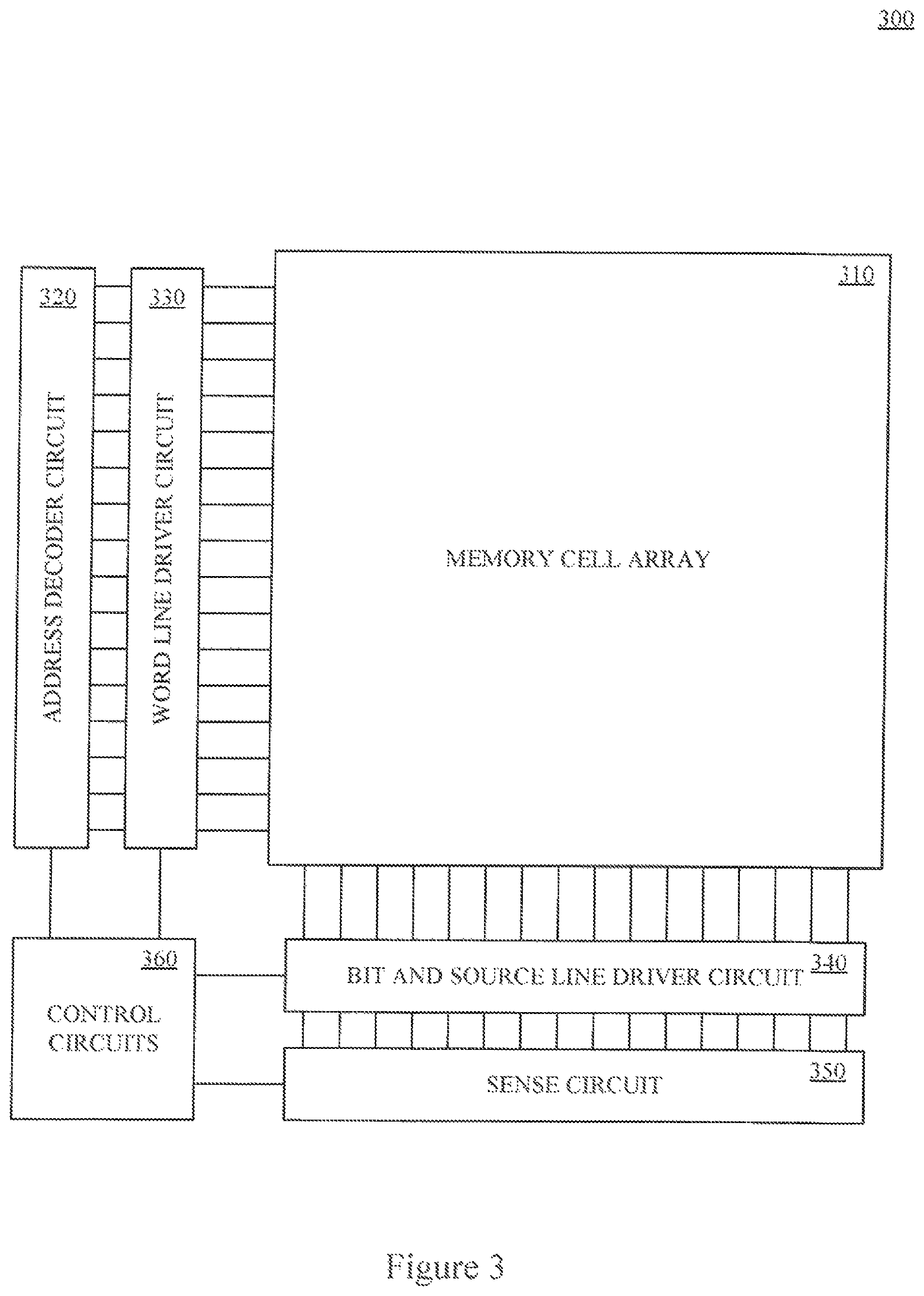
Referring now to FIG. 3, a block diagram of a Magnetoresistive Random Access Memory (MRAM), in accordance with embodiments of the present technology, is shown. The MRAM 300 can include a memory cell array 310, an address decoder circuit 320, a word line driver circuit 330, a bit line and source line driver circuit 340, a sense circuit 350, and control circuit 360. The MRAM 300 can include other well-known circuits that are not necessary for an understanding of the present technology and therefore are not discussed herein.
The memory cell array 310 can include a plurality of memory cells organized in rows and columns, with sets of word lines, source lines and bit lines spanning the array of cells throughout the chip. The address decoder 320 can map a given memory address to a particular row of memory cells in the array. The output of the address decoder 320 can be input to the word line driver 330. The output of the word line driver 330 can drive the word lines to select a given word line of the array. The bit line and source line driver 340 and the sense circuit 350 utilize the source lines and bit lines of the array to read from and write to memory cells of a selected word line of the array.
In one implementation, the MRAM may be a Spin Transfer Torque Magnetoresistive Random Access Memory (STT-MRAM). In STT-MRAMs, spin-aligned electrons are utilized to switch the polarization state of the free magnetic layer. The spin transfer torque reduces the amount of current needed during writes.
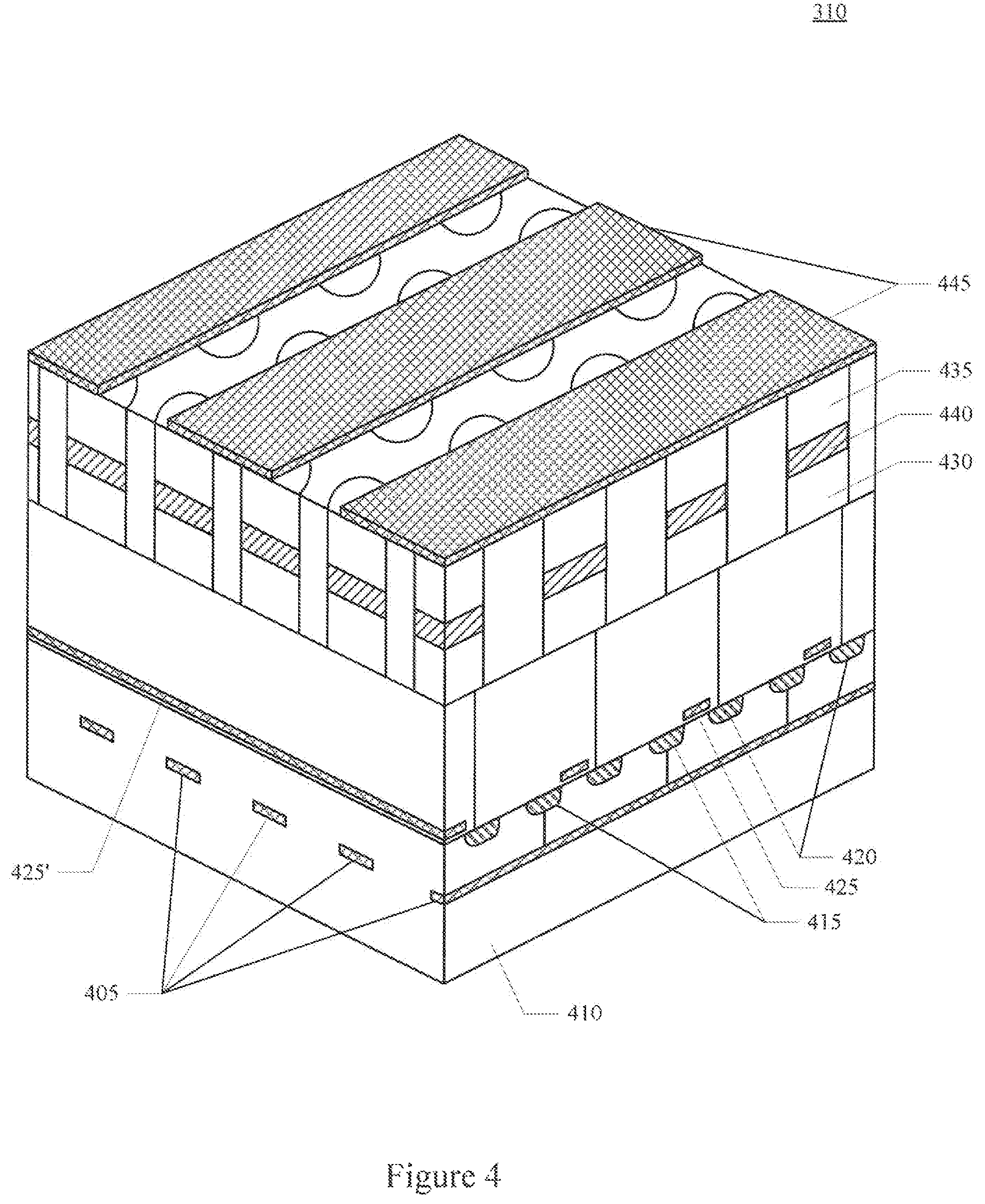
Operation of the Magnetoresistive Random Access Memory (MRAM) 300 will be further explained with reference to FIG. 4, which shows an isometric representation of a memory cell array 310, in accordance with embodiments of the present technology. Again, the memory cell array 310 can include a plurality of memory cells organized in rows and columns, with sets of word lines, source lines and bit lines. The MRAM as illustrated is not to scale and does not show every element of the MRAM. Instead, the illustration includes an arrangement of elements that readily facilitate an understanding of embodiments of the present technology.
The memory cell array 310 can include a plurality of source lines 405 disposed in a semiconductor substrate 410. The source lines 405 can be formed by a deep implant into the semiconductor substrate 410 through one or more masks to form buried source lines therein. Each memory cell can include a Magnetic Tunneling Junction (MTJ) and an access transistor arranged in an array of columns and rows. The access transistors can each include a source region 415, a drain region 420, a body region, a gate region 425 and a gate insulator region. The source and drain regions 415, 420 can be disposed in the semiconductor substrate 410. The source and drain regions 415, 420 can be formed by a shallow implant into the semiconductor substrate 410 through one or more masks. The gate region 425 can be disposed above a body region, between the respective source and drain regions 415, 420. The gate insulator region can be disposed between the gate region 425 and the body, source and drain regions 415, 420. The gate insulator regions and gate regions 425 can be formed by depositing one or more dielectric layers on the substrate 405, and one or more conductive layers on the one or more dielectric layers and then selectively etching the one or more conductive layers and dielectric layers utilizing one or more masks to form the gate insulator regions and the gate regions 425. The source regions 415 in each column of access transistors can be coupled to a respective source line 405. The gate regions 425 in each row of access transistors can be coupled to a respective word line, or the gate regions 425 can be integrally formed with the word lines 425' as illustrated in the figure. The drain regions 420 of the access transistors can be coupled to respective MTJs.
Each MTJ can include a reference magnetic layer 430, a free magnetic layer 435 and a magnetic tunneling barrier layer 440 disposed between the reference magnetic layer 430 and the free magnetic layer 435. The MJTs can be formed by depositing one or more seed layers, one or more synthetic antiferromagnetic layers, one or more reference magnetic layers 430, one or more magnetic tunneling barrier layers 440, one or more free magnetic layers 435, one or more non-magnetic spacer layers, one or more perpendicular polarizer layers, one or more capping layers, one or more hard mask layers, and then using the patterned hard mask layers to etch the other layers to form MJT pillars. The reference magnetic layer 430 can be coupled to the drain region 420 of the respective access transistor. The free magnetic layer 435 of two or more columns of MTJs can be coupled to a respective bit line 445.
The bit lines 445 can be disposed in one or more layers above the MTJ, and the source lines 405 can be disposed in one or more layers below the access transistors, along columns of the array. The bit lines 445 and source lines 405 can be substantially parallel to each other. The word lines 425' can be disposed in one or more layers along rows of the array. The word lines 425' can be substantially parallel to each other, and substantially perpendicular to the bit lines 445 and source lines 405. Two or more columns of the memory cells can be coupled to a respective bit line 445. Coupling a plurality of columns of the memory cells to respective bit lines 445 reduces the number of bit line in the memory cell array 310. By reducing the number of bit lines, the width of the bit lines can be increased and/or the spacing between bit lines can be increased for the same process technology. The increased width of the bit lines can, for example, reduce the resistance in the bit lines, and/or make alignment with the columns of MTJs easier. The increased spacing between bit lines can, for example, reduce manufacturing defects due alignment with the columns of MTJs, or shorting between adjacent bit lines. By reducing the number of bit lines, the density of the memory cells in the array can be increased due to smaller possible column pitch dimension for the same process technology. Furthermore, the physical length of the word lines in the memory cell array 310 can be reduced due to the smaller column pitch dimension. The reduced word line length can, for example, reduce the resistance in the word lines.
Referring now to both FIGS. 3 and 4, the control circuit 360 can be configured to cause the bit line and source line driver circuit 340 to apply appropriate write voltages to bit lines 445, source lines 405 and word lines 425' to write data to cells in a selected word. The magnetic polarity, and corresponding logic state, of the free layer 435 of the MTJ can be changed to one of two states depending upon the direction of current flowing through the MTJ. A logic `0` state can be written to a given cell by counter biasing the unselected source lines corresponding to the respective bit line for the given cell, as will be explained in more detail below.
For read operations, the control circuit 360 can be configured to cause the bit line and source line driver circuit 340 to apply appropriate read voltages to the bit lines 445, sources lines 405 and word lines 425' to cause a current to flow in the source lines 405 that can be sensed by the sense circuit 350 to read data from cells in a selected word. For configurations that sense the bit lines to read the memory cell states, a given cell can be read by counter biasing the unselected source lines corresponding to the respective bit line for the given cell, as will be explained in more detail below.
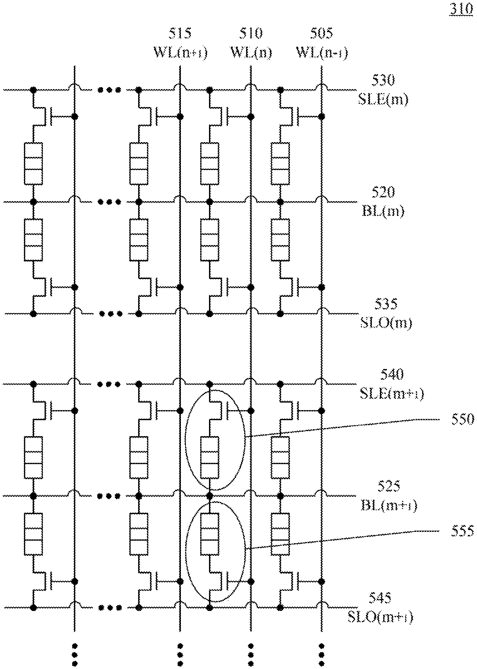
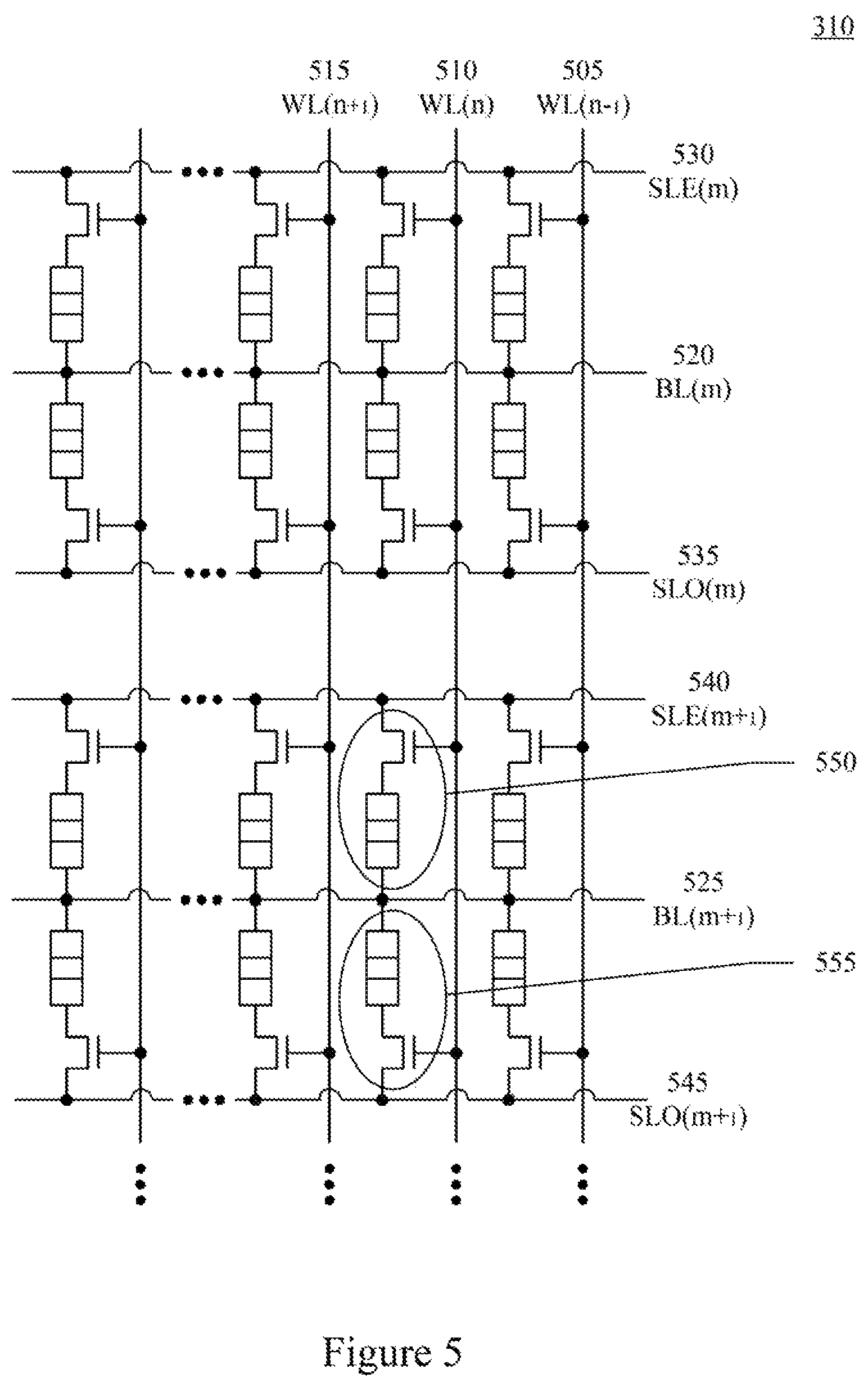
Operation of the Magnetoresistive Random Access Memory (MRAM) will be further explained with reference to FIG. 5, which shows a circuit diagram of a MRAM cell array, in accordance with embodiments of the present technology. The MRAM cell array 310 can include a plurality of memory cells, word lines 505-515, bit lines 520-525 and source lines 530-545. The word lines 505-515 of the memory cell array 310 can be organized along columns of the array. The bit lines 520-525 and source lines 530-545 can be organized along rows of the array. Each memory cell 550, 555 can comprise a Magnetic Tunneling Junction (MTJ) and an access transistor. The gates of the access transistors arranged along columns of the array can be coupled to respective word lines. The sources of the access transistors arranged along rows of the array can be coupled to respective source lines. The free magnetic layer of the MTJ arranged along two or more rows of the array can be coupled to a respective one of the bit lines.
Referring now to FIGS. 3, 4 and 5, the control circuit 360 can be configured to cause the word line driver to apply a predetermined voltage to a select word line. The control circuit 360 can also cause the bit line and source line driver circuit 340 to apply predetermined write voltages to the bit lines and source lines to write data to cells in the selected word. The magnetic polarity, and corresponding logic state, of the free layer of the MTJ can be changed to one of two states depending upon the direction of current from through the MTJ.
In a first example, the control circuit 360 can be configured to control the word line driver and the bit line and source line driver circuit 340, in accordance with Table 1. To read data from a given memory cell 550, the respective bit line BL(m+1) 525 can be biased at a bit line read potential (e.g., V.sub.BLR), the respective one of the pair of source lines SLE(m+1) 540 can be biased at ground (e.g., 0) and the other one of the pair of source lines SLO(m+1) 545 can also be biased at the bit line read potential (e.g., V.sub.BLR) or other potential that will prevent current from flowing in the other one of the pair of source lines. When the respective word line WL(n) 510 is biased at a word line read potential (e.g., V.sub.WLR) a current proportional to the resistance of the MTJ of the cell 550 will flow from the respective bit line BL(m+1) to the respective one of the pair of source lines SLO(m+1) 545. However, the other one of the pair of source lines SLO(m+1) 545 can be biased at the bit line read potential (e.g., V.sub.BLR) or other appropriate potential to prevent current from flowing in the respective bit line BL(m+1) 525 proportional to the resistance of the MTJ of the other cell 555 coupled to the bit line BL(m+1) 525. In such case, the current sensed on the respective bit line BL(m+1) 525 can indicate the state of the selected cell 550.
To write a logic `0` state to the given memory cell 550, the respective bit line BL(m+1) 525 can be biased at a bit line write potential (e.g., V.sub.BLW), the respective one of the pair of source lines SLE(m+1) 540 can be biased at ground (e.g., 0), and the other one of the pair of source lines SLO(m+1) 545 can also be biased at the bit line write potential (e.g., V.sub.BLW) or other potential that will prevent the cell 555 on the other one of the pair of source lines from being written to. When the respective word line WL(n) 510 is biased at a word line write potential (e.g., V.sub.WLW) a resulting current flowing through the MTJ of the cell 550 will cause the free magnetic layer into a state corresponding to a logic `0` state. However, the other one of the pair of source lines SLO(m+1) 545 biased at the bit line write potential (e.g., V.sub.BLR) or other appropriate potential voltage will prevent current from flowing through the MTJ of the other cell 555 coupled to the other one of the pair of bit lines BL(m+1) 525.
To write a logic `1` state to the given memory cell 550, the respective bit line BL(m+1) 525 can be biased at ground (e.g., 0), the respective one of the pair of source lines SLE(m+1) 540 can be biased at a source line write potential (e.g., V.sub.SLW), and the other one of the pair of source lines SLO(m+1) 545 can be biased at ground (e.g., 0). When the respective word line WL(n) 510 is biased at a word line write potential (e.g., V.sub.WLW) a resulting current flowing through the MTJ of the cell 550 will cause the free magnetic layer into a state corresponding to a logic `1` state.
TABLE-US-00001 TABLE 1 SLE SLO SLE SLO BL BL WL (m) (m) (m + 1) (m + 1) (m) (m + 1) (n) Standby 0 0 0 0 0 0 0 Read 0 0 0 V.sub.BLR 0 V.sub.BLR V.sub.WLR Write 0 0 0 0 V.sub.BLW 0 V.sub.BLW V.sub.WLW Write 1 0 0 V.sub.SLW 0 0 0 V.sub.WLW
In another example, the control circuit 360 can be configured to control the word line driver circuit 330 and the bit line and source line driver circuit 340 in accordance with Table 2 to read and write data to and from the memory cell array 310. To read data from a given memory cell 550, the respective bit line BL(m+1) 525 can be biased at ground (e.g., 0), the respective one of the pair of source lines SLE(m+1) 540 can be biased at a bit line read potential (e.g., V.sub.BLR) and the other one of the pair of source lines SLO(m+1) 545 can also be biased at ground (e.g., 0). When the respective word line WL(n) 510 is biased at a word line read potential (e.g., V.sub.WLR) a current proportional to the resistance of the MTJ of the given cell 550 will flow from the respective one of the pair of source lines SLE(m+1) 545 to the respective bit line BL(m+1). In such case, the current sensed on the respective source line SLE(m+1) 545 can indicate the state of the selected cell 550.
To write a logic `0` state to the given memory cell 550, the respective bit line BL(m+1) 525 can be biased at a bit line write potential (e.g., V.sub.BLW), the respective one of the pair of source lines SLE(m+1) 540 can be biased at ground (e.g., 0), and the other one of the pair of source lines SLO(m+1) 545 can also be biased at the bit line write potential (e.g., V.sub.BLW) or other potential that will prevent the cell 555 on the other one of the pair of source lines from being written to. When the respective word line WL(n) 510 is biased at a word line write potential (e.g., V.sub.WLW) a resulting current flowing through the MTJ of the cell 550 will cause the free magnetic layer into a state corresponding to a logic `0` state. However, the other one of the pair of source lines SLO(m+1) 545 biased at the bit line write potential (e.g., V.sub.BLR) or other appropriate potential voltage will prevent current from flowing through the MTJ of the other cell 555 coupled to the respective bit lines BL(m+1) 525.
To write a logic `1` state to the given memory cell 550, the respective bit line BL(m+1) 525 can be biased at ground (e.g., 0), the respective one of the pair of source lines SLE(m+1) 540 can be biased at a source line write potential (e.g., V.sub.SLW), and the other one of the pair of source lines SLO(m+1) 545 can be biased at ground (e.g., 0). When the respective word line WL(n) 510 is biased at a word line write potential (e.g., V.sub.WLW) a resulting current flowing through the MTJ of the cell 550 will cause the free magnetic layer into a state corresponding to a logic `1` state.
TABLE-US-00002 TABLE 2 SLE SLO SLE SLO BL BL WL (m) (m) (m + 1) (m + 1) (m) (m + 1) (n) Standby 0 0 0 0 0 0 0 Read 0 0 V.sub.BLR 0 0 0 V.sub.WLR Write 0 0 0 0 V.sub.BLW 0 V.sub.BLW V.sub.WLW Write 1 0 0 V.sub.SLW 0 0 0 V.sub.WLW
The above described read and write operations can be extended to embodiments wherein three or more columns of memory cells are coupled to a respective bit line, by counter biasing the one or more unselected source lines as appropriate.
Embodiments of the present technology advantageously reduce the number of bit lines in the memory cell array. In accordance with embodiments of the present technology, the one or more unselected source lines for the respective selected bit line can be counter biased to read from a given memory cell and writing a `0` state to the given memory cell, for bit line sense configurations. In source line sense configurations, the one or more unselected source lines for the respective bit line can be counter biased for writing a `0` state to the given memory cell. By reducing the number of bit lines, the pitch of the bit lines (e.g., bit line width and/or spacing between the bit lines) can advantageously be increased, Increasing the width of the bit lines can advantageously reduce the resistance in the bit lines. However, it may be advantageous to compensate for the reduction in bit line resistance so that the resistance of the bit lines and source lines more closely match each other. By reducing the number of bit lines, the density of the memory cells in the array can also be advantageously increased. By reducing the number of bit lines, the length of the word lines in the memory cell array can also be advantageously reduced, which can also advantageously reduce the resistance in the word lines.
The foregoing descriptions of specific embodiments of the present technology have been presented for purposes of illustration and description. They are not intended to be exhaustive or to limit the invention to the precise forms disclosed, and obviously many modifications and variations are possible in light of the above teaching. The embodiments were chosen and described in order to best explain the principles of the present technology and its practical application, to thereby enable others skilled in the art to best utilize the present technology and various embodiments with various modifications as are suited to the particular use contemplated. It is intended that the scope of the invention be defined by the claims appended hereto and their equivalents.
* * * * *
D00000
D00001
D00002
D00003
D00004
D00005
XML
uspto.report is an independent third-party trademark research tool that is not affiliated, endorsed, or sponsored by the United States Patent and Trademark Office (USPTO) or any other governmental organization. The information provided by uspto.report is based on publicly available data at the time of writing and is intended for informational purposes only.
While we strive to provide accurate and up-to-date information, we do not guarantee the accuracy, completeness, reliability, or suitability of the information displayed on this site. The use of this site is at your own risk. Any reliance you place on such information is therefore strictly at your own risk.
All official trademark data, including owner information, should be verified by visiting the official USPTO website at www.uspto.gov. This site is not intended to replace professional legal advice and should not be used as a substitute for consulting with a legal professional who is knowledgeable about trademark law.