Optical touch system comprising means for projecting and detecting light beams above and inside a transmissive panel
Wassvik , et al. De
U.S. patent number 10,496,227 [Application Number 15/547,587] was granted by the patent office on 2019-12-03 for optical touch system comprising means for projecting and detecting light beams above and inside a transmissive panel. This patent grant is currently assigned to FlatFrog Laboratories AB. The grantee listed for this patent is FlatFrog Laboratories AB. Invention is credited to Hakan Bergstrom, Thomas Craven-Bartle, Ivan Karlsson, Ola Wassvik.


| United States Patent | 10,496,227 |
| Wassvik , et al. | December 3, 2019 |
Optical touch system comprising means for projecting and detecting light beams above and inside a transmissive panel
Abstract
An embodiment of the invention provides a touch sensing apparatus, comprising: a light transmissive element (10) that defines a touch surface; a set of emitters (30a) arranged around the periphery of the touch surface to emit beams of light into the light transmissive element, wherein a first portion of the beams (50) of light propagate inside the light transmissive element while illuminating the touch surface such that an object touching the touch surface causes an attenuation of the propagating light, and wherein a second portion of the beams (90) of light pass out of the light transmissive element and are reflected to travel above the touch surface, a set of light detectors (30b) arranged around the periphery of the touch surface to receive light from the set of emitters from the transmissive element and from above the touch surface, wherein each light detector is arranged to receive light from more than one emitter.
| Inventors: | Wassvik; Ola (Ryssby, SE), Bergstrom; Hakan (Torna-hallestad, SE), Karlsson; Ivan (Lund, SE), Craven-Bartle; Thomas (Sodra Sandby, SE) | ||||||||||
|---|---|---|---|---|---|---|---|---|---|---|---|
| Applicant: |
|
||||||||||
| Assignee: | FlatFrog Laboratories AB (Lund,
SE) |
||||||||||
| Family ID: | 56615022 | ||||||||||
| Appl. No.: | 15/547,587 | ||||||||||
| Filed: | February 9, 2016 | ||||||||||
| PCT Filed: | February 09, 2016 | ||||||||||
| PCT No.: | PCT/SE2016/050098 | ||||||||||
| 371(c)(1),(2),(4) Date: | July 31, 2017 | ||||||||||
| PCT Pub. No.: | WO2016/130074 | ||||||||||
| PCT Pub. Date: | August 18, 2016 |
Prior Publication Data
| Document Identifier | Publication Date | |
|---|---|---|
| US 20180267672 A1 | Sep 20, 2018 | |
Foreign Application Priority Data
| Feb 9, 2015 [SE] | 1550145 | |||
| Current U.S. Class: | 1/1 |
| Current CPC Class: | G06F 3/0421 (20130101); G06F 3/0428 (20130101); G06F 1/3231 (20130101); G06F 1/3262 (20130101); G06F 2203/04102 (20130101); G06F 2203/04106 (20130101); G06F 2203/04108 (20130101); Y02D 10/00 (20180101); Y02D 10/173 (20180101); G06F 2203/04109 (20130101); G06F 2203/04104 (20130101) |
| Current International Class: | G06F 3/042 (20060101); G06F 1/3231 (20190101); G06F 1/3234 (20190101) |
References Cited [Referenced By]
U.S. Patent Documents
| 3440426 | April 1969 | Bush |
| 3553680 | January 1971 | Cooreman |
| 3673327 | June 1972 | Johnson et al. |
| 4129384 | December 1978 | Walker et al. |
| 4180702 | December 1979 | Sick et al. |
| 4209255 | June 1980 | Heynau et al. |
| 4213707 | July 1980 | Evans, Jr. |
| 4254333 | March 1981 | Bergstrom |
| 4254407 | March 1981 | Tipon |
| 4294543 | October 1981 | Apple et al. |
| 4346376 | August 1982 | Mallos |
| 4420261 | December 1983 | Barlow et al. |
| 4484179 | November 1984 | Kasday |
| 4507557 | March 1985 | Tsikos |
| 4521112 | June 1985 | Kuwabara et al. |
| 4542375 | September 1985 | Alles et al. |
| 4550250 | October 1985 | Mueller et al. |
| 4593191 | June 1986 | Alles |
| 4673918 | June 1987 | Adler et al. |
| 4688933 | August 1987 | Lapeyre |
| 4688993 | August 1987 | Ferris et al. |
| 4692809 | September 1987 | Beining et al. |
| 4710760 | December 1987 | Kasday |
| 4736191 | April 1988 | Matzke et al. |
| 4737626 | April 1988 | Hasegawa |
| 4746770 | May 1988 | McAvinney |
| 4752655 | June 1988 | Tajiri et al. |
| 4772763 | September 1988 | Garwin et al. |
| 4782328 | November 1988 | Denlinger |
| 4812833 | March 1989 | Shimauchi |
| 4837430 | June 1989 | Hasegawa |
| 4868912 | September 1989 | Doering |
| 4891829 | January 1990 | Deckman et al. |
| 4933544 | June 1990 | Tamaru |
| 4949079 | August 1990 | Loebner |
| 4986662 | January 1991 | Bures |
| 4988983 | January 1991 | Wehrer |
| 5065185 | November 1991 | Powers et al. |
| 5073770 | December 1991 | Lowbner |
| 5105186 | April 1992 | May |
| 5159322 | October 1992 | Loebner |
| 5166668 | November 1992 | Aoyagi |
| 5227622 | July 1993 | Suzuki |
| 5248856 | September 1993 | Mallicoat |
| 5254407 | October 1993 | Sergerie et al. |
| 5345490 | September 1994 | Finnigan et al. |
| 5383022 | January 1995 | Kaser |
| 5483261 | January 1996 | Yasutake |
| 5484966 | January 1996 | Segen |
| 5499098 | March 1996 | Ogawa |
| 5502568 | March 1996 | Ogawa et al. |
| 5525764 | June 1996 | Junkins et al. |
| 5526422 | June 1996 | Keen |
| 5570181 | October 1996 | Yasuo et al. |
| 5572251 | November 1996 | Ogawa |
| 5577501 | November 1996 | Flohr et al. |
| 5600105 | February 1997 | Fukuzaki et al. |
| 5672852 | September 1997 | Fukuzaki et al. |
| 5679930 | October 1997 | Katsurahira |
| 5686942 | November 1997 | Ball |
| 5688933 | November 1997 | Evans et al. |
| 5729249 | March 1998 | Yasutake |
| 5736686 | April 1998 | Perret, Jr. et al. |
| 5740224 | April 1998 | Muller et al. |
| 5764223 | June 1998 | Chang et al. |
| 5767517 | June 1998 | Hawkins |
| 5775792 | July 1998 | Wiese |
| 5945980 | August 1999 | Moissev et al. |
| 5945981 | August 1999 | Paull et al. |
| 5959617 | September 1999 | Bird et al. |
| 6061177 | May 2000 | Fujimoto |
| 6067079 | May 2000 | Shieh |
| 6122394 | September 2000 | Neukermans et al. |
| 6141104 | October 2000 | Schulz et al. |
| 6172667 | January 2001 | Sayag |
| 6227667 | May 2001 | Halldorsson et al. |
| 6229529 | May 2001 | Yano et al. |
| 6333735 | December 2001 | Anvekar |
| 6366276 | April 2002 | Kunimatsu et al. |
| 6380732 | April 2002 | Gilboa |
| 6380740 | April 2002 | Laub |
| 6390370 | May 2002 | Plesko |
| 6429857 | August 2002 | Masters et al. |
| 6452996 | September 2002 | Hsieh |
| 6476797 | November 2002 | Kurihara et al. |
| 6492633 | December 2002 | Nakazawa et al. |
| 6495832 | December 2002 | Kirby |
| 6504143 | January 2003 | Koops et al. |
| 6529327 | March 2003 | Graindorge |
| 6538644 | March 2003 | Muraoka |
| 6587099 | July 2003 | Takekawa |
| 6648485 | November 2003 | Colgan et al. |
| 6660964 | December 2003 | Benderly |
| 6664498 | December 2003 | Forsman et al. |
| 6664952 | December 2003 | Iwamoto et al. |
| 6690363 | February 2004 | Newton |
| 6707027 | March 2004 | Liess et al. |
| 6738051 | May 2004 | Boyd et al. |
| 6748098 | June 2004 | Rosenfeld |
| 6784948 | August 2004 | Kawashima et al. |
| 6799141 | September 2004 | Stoustrup et al. |
| 6806871 | October 2004 | Yasue |
| 6927384 | August 2005 | Reime et al. |
| 6940286 | September 2005 | Wang et al. |
| 6965836 | November 2005 | Richardson |
| 6972753 | December 2005 | Kimura et al. |
| 6985137 | January 2006 | Kaikuranta |
| 7042444 | May 2006 | Cok |
| 7084859 | August 2006 | Pryor |
| 7133031 | November 2006 | Wang et al. |
| 7176904 | February 2007 | Satoh |
| 7359041 | April 2008 | Xie et al. |
| 7397418 | July 2008 | Doerry et al. |
| 7432893 | October 2008 | Ma et al. |
| 7435940 | October 2008 | Eliasson et al. |
| 7442914 | October 2008 | Eliasson et al. |
| 7465914 | December 2008 | Eliasson et al. |
| 7613375 | November 2009 | Shimizu |
| 7629968 | December 2009 | Miller et al. |
| 7646833 | January 2010 | He et al. |
| 7653883 | January 2010 | Hotelling et al. |
| 7655901 | February 2010 | Idzik et al. |
| 7705835 | April 2010 | Eikman |
| 7847789 | December 2010 | Kolmykov-Zotov et al. |
| 7855716 | December 2010 | McCreary et al. |
| 7859519 | December 2010 | Tulbert |
| 7924272 | April 2011 | Boer et al. |
| 7932899 | April 2011 | Newton et al. |
| 7969410 | June 2011 | Kakarala |
| 7995039 | August 2011 | Eliasson et al. |
| 8013845 | September 2011 | Ostergaard et al. |
| 8031186 | October 2011 | Ostergaard |
| 8077147 | December 2011 | Krah et al. |
| 8093545 | January 2012 | Leong et al. |
| 8094136 | January 2012 | Eliasson et al. |
| 8094910 | January 2012 | Xu |
| 8149211 | April 2012 | Hayakawa et al. |
| 8218154 | July 2012 | Ostergaard et al. |
| 8274495 | September 2012 | Lee |
| 8325158 | December 2012 | Yatsuda et al. |
| 8339379 | December 2012 | Goertz et al. |
| 8350827 | January 2013 | Chung et al. |
| 8384010 | February 2013 | Hong et al. |
| 8407606 | March 2013 | Davidson et al. |
| 8441467 | May 2013 | Han |
| 8445834 | May 2013 | Hong et al. |
| 8466901 | June 2013 | Yen et al. |
| 8482547 | July 2013 | Cobon et al. |
| 8542217 | September 2013 | Wassvik et al. |
| 8553014 | October 2013 | Holmgren |
| 8567257 | October 2013 | Van Steenberge et al. |
| 8581884 | November 2013 | Fahraeus et al. |
| 8624858 | January 2014 | Fyke et al. |
| 8686974 | April 2014 | Christiansson et al. |
| 8692807 | April 2014 | Fohraeus et al. |
| 8716614 | May 2014 | Wassvik |
| 8727581 | May 2014 | Saccomanno |
| 8745514 | June 2014 | Davidson |
| 8780066 | July 2014 | Christiansson et al. |
| 8830181 | September 2014 | Clark et al. |
| 8860696 | October 2014 | Wassvik et al. |
| 8872098 | October 2014 | Bergstrom et al. |
| 8872801 | October 2014 | Bergstrom et al. |
| 8884900 | November 2014 | Wassvik |
| 8890843 | November 2014 | Wassvik et al. |
| 8890849 | November 2014 | Christiansson et al. |
| 8928590 | January 2015 | El Dokor |
| 8963886 | February 2015 | Wassvik |
| 8982084 | March 2015 | Christiansson et al. |
| 9024916 | May 2015 | Christiansson |
| 9035909 | May 2015 | Christiansson |
| 9063617 | June 2015 | Eliasson et al. |
| 9086763 | July 2015 | Johansson et al. |
| 9134854 | September 2015 | Wassvik et al. |
| 9158401 | October 2015 | Christiansson |
| 9158415 | October 2015 | Song et al. |
| 9213445 | December 2015 | King et al. |
| 9274645 | March 2016 | Christiansson et al. |
| 9317168 | April 2016 | Christiansson et al. |
| 9323396 | April 2016 | Han et al. |
| 9366565 | June 2016 | Uvnas |
| 9377884 | June 2016 | Christiansson et al. |
| 9389732 | July 2016 | Craven-Bartle |
| 9411444 | August 2016 | Christiansson et al. |
| 9411464 | August 2016 | Wallander et al. |
| 9430079 | August 2016 | Christiansson et al. |
| 9442574 | September 2016 | Fahraeus et al. |
| 9547393 | January 2017 | Christiansson et al. |
| 9552103 | January 2017 | Craven-Bartle et al. |
| 9557846 | January 2017 | Baharav et al. |
| 9588619 | March 2017 | Christiansson et al. |
| 9594467 | March 2017 | Christiansson et al. |
| 9626018 | April 2017 | Christiansson et al. |
| 9626040 | April 2017 | Wallander et al. |
| 9639210 | May 2017 | Wallander et al. |
| 9678602 | June 2017 | Wallander |
| 9684414 | June 2017 | Christiansson et al. |
| 9710101 | July 2017 | Christiansson et al. |
| 2001/0002694 | June 2001 | Nakazawa et al. |
| 2001/0005004 | June 2001 | Shiratsuki et al. |
| 2001/0005308 | June 2001 | Oishi et al. |
| 2001/0030642 | October 2001 | Sullivan et al. |
| 2002/0067348 | June 2002 | Masters et al. |
| 2002/0075243 | June 2002 | Newton |
| 2002/0118177 | August 2002 | Newton |
| 2002/0158823 | October 2002 | Zavracky et al. |
| 2002/0158853 | October 2002 | Sugawara et al. |
| 2002/0163505 | November 2002 | Takekawa |
| 2003/0016450 | January 2003 | Bluemel et al. |
| 2003/0034439 | February 2003 | Reime et al. |
| 2003/0034935 | February 2003 | Amanai et al. |
| 2003/0048257 | March 2003 | Mattila |
| 2003/0052257 | March 2003 | Sumriddetchkajorn |
| 2003/0095399 | May 2003 | Grenda et al. |
| 2003/0107748 | June 2003 | Lee |
| 2003/0137494 | July 2003 | Tulbert |
| 2003/0156100 | August 2003 | Gettemy |
| 2003/0160155 | August 2003 | Liess |
| 2003/0210537 | November 2003 | Engelmann |
| 2003/0214486 | November 2003 | Roberts |
| 2004/0027339 | February 2004 | Schulz |
| 2004/0032401 | February 2004 | Nakazawa et al. |
| 2004/0090432 | May 2004 | Takahashi et al. |
| 2004/0130338 | July 2004 | Wang et al. |
| 2004/0174541 | September 2004 | Freifeld |
| 2004/0201579 | October 2004 | Graham |
| 2004/0212603 | October 2004 | Cok |
| 2004/0238627 | December 2004 | Silverbrook et al. |
| 2004/0239702 | December 2004 | Kang et al. |
| 2004/0245438 | December 2004 | Payne et al. |
| 2004/0252091 | December 2004 | Ma et al. |
| 2004/0252867 | December 2004 | Lan et al. |
| 2005/0012714 | January 2005 | Russo et al. |
| 2005/0041013 | February 2005 | Tanaka |
| 2005/0057903 | March 2005 | Choi |
| 2005/0073508 | April 2005 | Pittel et al. |
| 2005/0083293 | April 2005 | Dixon |
| 2005/0128190 | June 2005 | Ryynanen |
| 2005/0143923 | June 2005 | Keers et al. |
| 2005/0156914 | July 2005 | Lipman et al. |
| 2005/0162398 | July 2005 | Eliasson et al. |
| 2005/0179977 | August 2005 | Chui et al. |
| 2005/0200613 | September 2005 | Kobayashi et al. |
| 2005/0212774 | September 2005 | Ho et al. |
| 2005/0248540 | November 2005 | Newton |
| 2005/0253834 | November 2005 | Sakamaki et al. |
| 2005/0276053 | December 2005 | Nortrup et al. |
| 2006/0001650 | January 2006 | Robbins et al. |
| 2006/0001653 | January 2006 | Smits |
| 2006/0007185 | January 2006 | Kobayashi |
| 2006/0008164 | January 2006 | Wu et al. |
| 2006/0017706 | January 2006 | Cutherell et al. |
| 2006/0017709 | January 2006 | Okano |
| 2006/0033725 | February 2006 | Marggraff et al. |
| 2006/0038698 | February 2006 | Chen |
| 2006/0061861 | March 2006 | Munro et al. |
| 2006/0114237 | June 2006 | Crockett et al. |
| 2006/0132454 | June 2006 | Chen et al. |
| 2006/0139340 | June 2006 | Geaghan |
| 2006/0158437 | July 2006 | Blythe et al. |
| 2006/0170658 | August 2006 | Nakamura et al. |
| 2006/0202974 | September 2006 | Thielman |
| 2006/0227120 | October 2006 | Eikman |
| 2006/0255248 | November 2006 | Eliasson |
| 2006/0256092 | November 2006 | Lee |
| 2006/0279558 | December 2006 | Van Delden et al. |
| 2006/0281543 | December 2006 | Sutton et al. |
| 2006/0290684 | December 2006 | Giraldo et al. |
| 2007/0014486 | January 2007 | Schiwietz et al. |
| 2007/0024598 | February 2007 | Miller et al. |
| 2007/0034783 | February 2007 | Eliasson et al. |
| 2007/0038691 | February 2007 | Candes et al. |
| 2007/0052684 | March 2007 | Gruhlke et al. |
| 2007/0070056 | March 2007 | Sato et al. |
| 2007/0075648 | April 2007 | Blythe et al. |
| 2007/0120833 | May 2007 | Yamaguchi et al. |
| 2007/0125937 | June 2007 | Eliasson et al. |
| 2007/0152985 | July 2007 | Ostergaard et al. |
| 2007/0201042 | August 2007 | Eliasson et al. |
| 2007/0296688 | December 2007 | Nakamura et al. |
| 2008/0006766 | January 2008 | Oon et al. |
| 2008/0007540 | January 2008 | Ostergaard |
| 2008/0007541 | January 2008 | Eliasson et al. |
| 2008/0007542 | January 2008 | Eliasson et al. |
| 2008/0011944 | January 2008 | Chua et al. |
| 2008/0029691 | February 2008 | Han |
| 2008/0036743 | February 2008 | Westerman et al. |
| 2008/0062150 | March 2008 | Lee |
| 2008/0068691 | March 2008 | Miyatake |
| 2008/0074401 | March 2008 | Chung et al. |
| 2008/0088603 | April 2008 | Eliasson et al. |
| 2008/0121442 | May 2008 | Boer et al. |
| 2008/0122792 | May 2008 | Izadi et al. |
| 2008/0122803 | May 2008 | Izadi et al. |
| 2008/0130979 | June 2008 | Run et al. |
| 2008/0150846 | June 2008 | Chung et al. |
| 2008/0150848 | June 2008 | Chung et al. |
| 2008/0151126 | June 2008 | Yu |
| 2008/0158176 | July 2008 | Land et al. |
| 2008/0189046 | August 2008 | Eliasson et al. |
| 2008/0192025 | August 2008 | Jaeger et al. |
| 2008/0238433 | October 2008 | Joutsenoja et al. |
| 2008/0246388 | October 2008 | Cheon et al. |
| 2008/0252619 | October 2008 | Crockett et al. |
| 2008/0266266 | October 2008 | Kent et al. |
| 2008/0278460 | November 2008 | Arnett et al. |
| 2008/0284925 | November 2008 | Han |
| 2008/0291668 | November 2008 | Aylward et al. |
| 2008/0297482 | December 2008 | Weiss |
| 2009/0002340 | January 2009 | Van Genechten |
| 2009/0006292 | January 2009 | Block |
| 2009/0040786 | February 2009 | Mori |
| 2009/0066647 | March 2009 | Kerr et al. |
| 2009/0067178 | March 2009 | Huang et al. |
| 2009/0073142 | March 2009 | Yamashita et al. |
| 2009/0077501 | March 2009 | Partridge et al. |
| 2009/0085894 | April 2009 | Gandhi et al. |
| 2009/0091554 | April 2009 | Keam |
| 2009/0115919 | May 2009 | Tanaka et al. |
| 2009/0122020 | May 2009 | Eliasson et al. |
| 2009/0122027 | May 2009 | Newton |
| 2009/0128508 | May 2009 | Sohn et al. |
| 2009/0135162 | May 2009 | Van De Wijdeven |
| 2009/0143141 | June 2009 | Wells et al. |
| 2009/0153519 | June 2009 | Suarez Rovere |
| 2009/0161026 | June 2009 | Wu et al. |
| 2009/0168459 | July 2009 | Holman et al. |
| 2009/0187842 | July 2009 | Collins et al. |
| 2009/0189857 | July 2009 | Benko et al. |
| 2009/0189874 | July 2009 | Chene et al. |
| 2009/0189878 | July 2009 | Goertz et al. |
| 2009/0219256 | September 2009 | Newton |
| 2009/0229892 | September 2009 | Fisher et al. |
| 2009/0251439 | October 2009 | Westerman et al. |
| 2009/0256817 | October 2009 | Perlin et al. |
| 2009/0259967 | October 2009 | Davidson et al. |
| 2009/0267919 | October 2009 | Chao et al. |
| 2009/0273794 | November 2009 | Ostergaard et al. |
| 2009/0278816 | November 2009 | Colson |
| 2009/0297009 | December 2009 | Xu et al. |
| 2010/0033444 | February 2010 | Kobayashi |
| 2010/0045629 | February 2010 | Newton |
| 2010/0060896 | March 2010 | Van De Wijdeven et al. |
| 2010/0066016 | March 2010 | Van De Wijdeven et al. |
| 2010/0066704 | March 2010 | Kasai |
| 2010/0073318 | March 2010 | Hu et al. |
| 2010/0078545 | April 2010 | Leong et al. |
| 2010/0079407 | April 2010 | Suggs et al. |
| 2010/0079408 | April 2010 | Leong et al. |
| 2010/0097345 | April 2010 | Jang et al. |
| 2010/0097348 | April 2010 | Park et al. |
| 2010/0097353 | April 2010 | Newton |
| 2010/0125438 | May 2010 | Audet |
| 2010/0127975 | May 2010 | Jensen |
| 2010/0134435 | June 2010 | Kimura et al. |
| 2010/0142823 | June 2010 | Wang et al. |
| 2010/0187422 | July 2010 | Kothari et al. |
| 2010/0193259 | August 2010 | Wassvik |
| 2010/0229091 | September 2010 | Homma et al. |
| 2010/0238139 | September 2010 | Goertz et al. |
| 2010/0238686 | September 2010 | Weber |
| 2010/0245292 | September 2010 | Wu |
| 2010/0265170 | October 2010 | Norieda |
| 2010/0277436 | November 2010 | Feng et al. |
| 2010/0277728 | November 2010 | Imura |
| 2010/0283785 | November 2010 | Satulovsky |
| 2010/0284596 | November 2010 | Miao et al. |
| 2010/0289754 | November 2010 | Sleeman et al. |
| 2010/0295821 | November 2010 | Chang et al. |
| 2010/0302196 | December 2010 | Han et al. |
| 2010/0302209 | December 2010 | Large |
| 2010/0302210 | December 2010 | Han et al. |
| 2010/0302240 | December 2010 | Lettvin |
| 2010/0315379 | December 2010 | Allard et al. |
| 2010/0321328 | December 2010 | Chang et al. |
| 2010/0322550 | December 2010 | Trott |
| 2011/0007021 | January 2011 | Bernstein |
| 2011/0043490 | February 2011 | Powell et al. |
| 2011/0049388 | March 2011 | Delaney et al. |
| 2011/0050649 | March 2011 | Newton et al. |
| 2011/0051394 | March 2011 | Bailey |
| 2011/0068256 | March 2011 | Hong et al. |
| 2011/0069039 | March 2011 | Lee et al. |
| 2011/0069807 | March 2011 | Dennerlein et al. |
| 2011/0074725 | March 2011 | Westerman et al. |
| 2011/0074734 | March 2011 | Wassvik |
| 2011/0074735 | March 2011 | Wassvik et al. |
| 2011/0090176 | April 2011 | Christiansson et al. |
| 2011/0102320 | May 2011 | Hauke |
| 2011/0102374 | May 2011 | Wassvik et al. |
| 2011/0115748 | May 2011 | Xu |
| 2011/0121323 | May 2011 | Wu et al. |
| 2011/0122075 | May 2011 | Seo et al. |
| 2011/0122091 | May 2011 | King et al. |
| 2011/0122094 | May 2011 | Tsang et al. |
| 2011/0134079 | June 2011 | Stark |
| 2011/0140106 | June 2011 | Forbes |
| 2011/0147569 | June 2011 | Drumm |
| 2011/0157095 | June 2011 | Drumm |
| 2011/0157096 | June 2011 | Drumm |
| 2011/0163996 | July 2011 | Wassvik et al. |
| 2011/0163997 | July 2011 | Kim |
| 2011/0163998 | July 2011 | Goertz et al. |
| 2011/0169780 | July 2011 | Goertz et al. |
| 2011/0175852 | July 2011 | Goertz et al. |
| 2011/0205186 | August 2011 | Newton et al. |
| 2011/0216042 | September 2011 | Wassvik et al. |
| 2011/0221705 | September 2011 | Yi |
| 2011/0221997 | September 2011 | Kim |
| 2011/0227036 | September 2011 | Vaufrey |
| 2011/0227874 | September 2011 | Fahraeus et al. |
| 2011/0234537 | September 2011 | Kim et al. |
| 2011/0254864 | October 2011 | Tsuchikawa et al. |
| 2011/0261020 | October 2011 | Song |
| 2011/0267296 | November 2011 | Noguchi et al. |
| 2011/0291989 | December 2011 | Lee |
| 2011/0298743 | December 2011 | Machida et al. |
| 2011/0309325 | December 2011 | Park et al. |
| 2011/0310045 | December 2011 | Toda et al. |
| 2012/0019448 | January 2012 | Pitkanen et al. |
| 2012/0026408 | February 2012 | Lee et al. |
| 2012/0038593 | February 2012 | Ronka et al. |
| 2012/0062474 | March 2012 | Weishaupt et al. |
| 2012/0068973 | March 2012 | Christiansson et al. |
| 2012/0086673 | April 2012 | Chien et al. |
| 2012/0089348 | April 2012 | Perlin et al. |
| 2012/0110447 | May 2012 | Chen |
| 2012/0131490 | May 2012 | Lin et al. |
| 2012/0141001 | June 2012 | Zhang et al. |
| 2012/0146930 | June 2012 | Lee |
| 2012/0146950 | June 2012 | Park |
| 2012/0153134 | June 2012 | Bergstrom et al. |
| 2012/0154338 | June 2012 | Bergstrom et al. |
| 2012/0162142 | June 2012 | Christiansson et al. |
| 2012/0162144 | June 2012 | Fahraeus et al. |
| 2012/0169672 | July 2012 | Christiansson |
| 2012/0181419 | July 2012 | Momtahan |
| 2012/0182266 | July 2012 | Han |
| 2012/0188206 | July 2012 | Sparf et al. |
| 2012/0191993 | July 2012 | Drader et al. |
| 2012/0200532 | August 2012 | Powell et al. |
| 2012/0200538 | August 2012 | Christiansson et al. |
| 2012/0212441 | August 2012 | Christiansson et al. |
| 2012/0217882 | August 2012 | Wong et al. |
| 2012/0249478 | October 2012 | Chang et al. |
| 2012/0256882 | October 2012 | Christiansson et al. |
| 2012/0268403 | October 2012 | Christiansson |
| 2012/0268427 | October 2012 | Slobodin |
| 2012/0274559 | November 2012 | Mathai et al. |
| 2012/0305755 | December 2012 | Hong et al. |
| 2013/0021300 | January 2013 | Wassvik |
| 2013/0021302 | January 2013 | Drumm |
| 2013/0027404 | January 2013 | Sarnoff |
| 2013/0044073 | February 2013 | Christiansson et al. |
| 2013/0055080 | February 2013 | Komer et al. |
| 2013/0076697 | March 2013 | Goertz et al. |
| 2013/0082980 | April 2013 | Gruhlke et al. |
| 2013/0107569 | May 2013 | Suganuma |
| 2013/0113715 | May 2013 | Grant et al. |
| 2013/0120320 | May 2013 | Liu et al. |
| 2013/0125016 | May 2013 | Pallakoff et al. |
| 2013/0127790 | May 2013 | Wassvik |
| 2013/0135258 | May 2013 | King et al. |
| 2013/0135259 | May 2013 | King et al. |
| 2013/0141388 | June 2013 | Ludwig et al. |
| 2013/0154983 | June 2013 | Christiansson et al. |
| 2013/0155027 | June 2013 | Holmgren |
| 2013/0181896 | July 2013 | Gruhlke et al. |
| 2013/0187891 | July 2013 | Eriksson |
| 2013/0201142 | August 2013 | Suarez Rovere |
| 2013/0222346 | August 2013 | Chen et al. |
| 2013/0241887 | September 2013 | Sharma |
| 2013/0249833 | September 2013 | Christiansson et al. |
| 2013/0269867 | October 2013 | Trott |
| 2013/0275082 | October 2013 | Follmer et al. |
| 2013/0285920 | October 2013 | Colley |
| 2013/0285968 | October 2013 | Christiansson et al. |
| 2013/0300716 | November 2013 | Craven-Bartle et al. |
| 2013/0307795 | November 2013 | Suarez Rovere |
| 2013/0342490 | December 2013 | Wallander et al. |
| 2014/0002400 | January 2014 | Christiansson et al. |
| 2014/0028575 | January 2014 | Parivar et al. |
| 2014/0028604 | January 2014 | Morinaga et al. |
| 2014/0028629 | January 2014 | Drumm et al. |
| 2014/0036203 | February 2014 | Guillou et al. |
| 2014/0055421 | February 2014 | Christiansson et al. |
| 2014/0063853 | March 2014 | Nichol et al. |
| 2014/0071653 | March 2014 | Thompson et al. |
| 2014/0085241 | March 2014 | Christiansson et al. |
| 2014/0092052 | April 2014 | Grunthaner et al. |
| 2014/0098032 | April 2014 | Ng et al. |
| 2014/0098058 | April 2014 | Baharav et al. |
| 2014/0109219 | April 2014 | Rohrweck et al. |
| 2014/0125633 | May 2014 | Fahraeus et al. |
| 2014/0160762 | June 2014 | Dudik et al. |
| 2014/0192023 | July 2014 | Hoffman |
| 2014/0232669 | August 2014 | Ohlsson et al. |
| 2014/0237401 | August 2014 | Krus et al. |
| 2014/0237408 | August 2014 | Ohlsson et al. |
| 2014/0237422 | August 2014 | Ohlsson et al. |
| 2014/0253831 | September 2014 | Craven-Bartle |
| 2014/0267124 | September 2014 | Christiansson et al. |
| 2014/0292701 | October 2014 | Christiansson et al. |
| 2014/0300572 | October 2014 | Ohlsson et al. |
| 2014/0320460 | October 2014 | Johansson et al. |
| 2014/0347325 | November 2014 | Wallander et al. |
| 2014/0362046 | December 2014 | Yoshida |
| 2014/0368471 | December 2014 | Christiansson et al. |
| 2014/0375607 | December 2014 | Christiansson et al. |
| 2015/0002386 | January 2015 | Mankowski et al. |
| 2015/0002470 | January 2015 | Zhu |
| 2015/0015497 | January 2015 | Leigh |
| 2015/0035774 | February 2015 | Christiansson et al. |
| 2015/0035803 | February 2015 | Wassvik et al. |
| 2015/0053850 | February 2015 | Uvnas |
| 2015/0054759 | February 2015 | Christiansson et al. |
| 2015/0083891 | March 2015 | Wallander |
| 2015/0103013 | April 2015 | Huang |
| 2015/0103051 | April 2015 | Wyrwas |
| 2015/0130769 | May 2015 | Bjorklund |
| 2015/0138105 | May 2015 | Christiansson et al. |
| 2015/0138158 | May 2015 | Wallander et al. |
| 2015/0138161 | May 2015 | Wassvik |
| 2015/0205441 | July 2015 | Bergstrom et al. |
| 2015/0215450 | July 2015 | Seo et al. |
| 2015/0242055 | August 2015 | Wallander |
| 2015/0317036 | November 2015 | Johansson et al. |
| 2015/0324028 | November 2015 | Wassvik et al. |
| 2015/0331544 | November 2015 | Bergstrom et al. |
| 2015/0331545 | November 2015 | Wassvik et al. |
| 2015/0331546 | November 2015 | Craven-Bartle et al. |
| 2015/0331547 | November 2015 | Wassvik et al. |
| 2015/0332655 | November 2015 | Krus et al. |
| 2015/0346856 | December 2015 | Wassvik |
| 2015/0346911 | December 2015 | Christiansson |
| 2015/0363042 | December 2015 | Krus et al. |
| 2016/0026337 | January 2016 | Wassvik et al. |
| 2016/0034099 | February 2016 | Christiansson et al. |
| 2016/0050746 | February 2016 | Wassvik et al. |
| 2016/0070415 | March 2016 | Christiansson et al. |
| 2016/0070416 | March 2016 | Wassvik |
| 2016/0124546 | May 2016 | Chen et al. |
| 2016/0124551 | May 2016 | Christiansson et al. |
| 2016/0154531 | June 2016 | Wall |
| 2016/0202841 | July 2016 | Christiansson et al. |
| 2016/0216844 | July 2016 | Bergstrom |
| 2016/0224144 | August 2016 | Klinghult et al. |
| 2016/0299593 | October 2016 | Christiansson et al. |
| 2016/0328090 | November 2016 | Klinghult |
| 2016/0328091 | November 2016 | Wassvik et al. |
| 2016/0334942 | November 2016 | Wassvik |
| 2016/0342282 | November 2016 | Wassvik |
| 2016/0357348 | December 2016 | Wallander |
| 2017/0010688 | January 2017 | Fahraeus et al. |
| 2017/0090090 | March 2017 | Craven-Bartle et al. |
| 2017/0102827 | April 2017 | Christiansson et al. |
| 2017/0115235 | April 2017 | Ohlsson et al. |
| 2017/0139541 | May 2017 | Christiansson et al. |
| 2017/0177163 | June 2017 | Wallander et al. |
| 2017/0185230 | June 2017 | Wallander et al. |
| 2008 280 952 | Mar 2009 | AU | |||
| 201233592 | May 2009 | CN | |||
| 101644854 | Feb 2010 | CN | |||
| 201437963 | Apr 2010 | CN | |||
| 101019071 | Jun 2012 | CN | |||
| 101206550 | Jun 2012 | CN | |||
| 101075168 | Apr 2014 | CN | |||
| 3511330 | May 1988 | DE | |||
| 68902419 | Mar 1993 | DE | |||
| 69000920 | Jun 1993 | DE | |||
| 19809934 | Sep 1999 | DE | |||
| 10026201 | Dec 2000 | DE | |||
| 102010000473 | Aug 2010 | DE | |||
| 0845812 | Jun 1998 | EP | |||
| 0600576 | Oct 1998 | EP | |||
| 1798630 | Jun 2007 | EP | |||
| 0897161 | Oct 2007 | EP | |||
| 2088501 | Aug 2009 | EP | |||
| 1512989 | Sep 2009 | EP | |||
| 2077490 | Jan 2010 | EP | |||
| 1126236 | Dec 2010 | EP | |||
| 2314203 | Apr 2011 | EP | |||
| 2339437 | Oct 2011 | EP | |||
| 2442180 | Apr 2012 | EP | |||
| 2466429 | Jun 2012 | EP | |||
| 2479642 | Jul 2012 | EP | |||
| 1457870 | Aug 2012 | EP | |||
| 2778849 | Sep 2014 | EP | |||
| 2172828 | Oct 1973 | FR | |||
| 2617619 | Jan 1990 | FR | |||
| 2614711 | Mar 1992 | FR | |||
| 2617620 | Sep 1992 | FR | |||
| 2676275 | Nov 1992 | FR | |||
| 1380144 | Jan 1975 | GB | |||
| 2131544 | Mar 1986 | GB | |||
| 2204126 | Nov 1988 | GB | |||
| 2000506655 | May 2000 | JP | |||
| 2000172438 | Jun 2000 | JP | |||
| 2000259334 | Sep 2000 | JP | |||
| 2000293311 | Oct 2000 | JP | |||
| 2003330603 | Nov 2003 | JP | |||
| 2005004278 | Jan 2005 | JP | |||
| 2008506173 | Feb 2008 | JP | |||
| 2011530124 | Dec 2011 | JP | |||
| 100359400 | Jul 2001 | KR | |||
| 100940435 | Feb 2010 | KR | |||
| WO 1984/003186 | Aug 1984 | WO | |||
| WO 1999/046602 | Sep 1999 | WO | |||
| WO 01/127867 | Apr 2001 | WO | |||
| WO 01/84251 | Nov 2001 | WO | |||
| WO 02/35460 | May 2002 | WO | |||
| WO 02/077915 | Oct 2002 | WO | |||
| WO 02/095668 | Nov 2002 | WO | |||
| WO 03/076870 | Sep 2003 | WO | |||
| WO 2004/081502 | Sep 2004 | WO | |||
| WO 2004/081956 | Sep 2004 | WO | |||
| WO 2005/026938 | Mar 2005 | WO | |||
| WO 2005/029172 | Mar 2005 | WO | |||
| WO 2005/029395 | Mar 2005 | WO | |||
| WO 2005/125011 | Dec 2005 | WO | |||
| WO 2006/095320 | Sep 2006 | WO | |||
| WO 2006/124551 | Nov 2006 | WO | |||
| WO 2007/003196 | Jan 2007 | WO | |||
| WO 2007/058924 | May 2007 | WO | |||
| WO 2007/112742 | Oct 2007 | WO | |||
| WO 2008/004103 | Jan 2008 | WO | |||
| WO 2008/007276 | Jan 2008 | WO | |||
| WO 2008/017077 | Feb 2008 | WO | |||
| WO 2008/039006 | Apr 2008 | WO | |||
| WO 2008/068607 | Jun 2008 | WO | |||
| WO 2006/124551 | Jul 2008 | WO | |||
| WO 2008/017077 | Feb 2009 | WO | |||
| WO 2009/048365 | Apr 2009 | WO | |||
| WO 2009/077962 | Jun 2009 | WO | |||
| WO 2009/102681 | Aug 2009 | WO | |||
| WO 2009/137355 | Nov 2009 | WO | |||
| WO 2010/006882 | Jan 2010 | WO | |||
| WO 2010/006883 | Jan 2010 | WO | |||
| WO 2010/006884 | Jan 2010 | WO | |||
| WO 2010/006885 | Jan 2010 | WO | |||
| WO 2010/006886 | Jan 2010 | WO | |||
| WO 2010/015408 | Feb 2010 | WO | |||
| WO 2010/046539 | Apr 2010 | WO | |||
| WO 2010/056177 | May 2010 | WO | |||
| WO 2010/064983 | Jun 2010 | WO | |||
| WO 2010/081702 | Jul 2010 | WO | |||
| WO 2010/112404 | Oct 2010 | WO | |||
| WO 2010/123809 | Oct 2010 | WO | |||
| WO 2010/134865 | Nov 2010 | WO | |||
| WO 2011/028169 | Mar 2011 | WO | |||
| WO 2011/028170 | Mar 2011 | WO | |||
| WO 2011/049511 | Apr 2011 | WO | |||
| WO 2011/049512 | Apr 2011 | WO | |||
| WO 2011/049513 | Apr 2011 | WO | |||
| WO 2011/057572 | May 2011 | WO | |||
| WO 2011/078769 | Jun 2011 | WO | |||
| WO 2011/082477 | Jul 2011 | WO | |||
| WO 2011/139213 | Nov 2011 | WO | |||
| WO 2012/002894 | Jan 2012 | WO | |||
| WO 2012/010078 | Jan 2012 | WO | |||
| WO 2012/050510 | Apr 2012 | WO | |||
| WO 2012/082055 | Jun 2012 | WO | |||
| WO 2012/105893 | Aug 2012 | WO | |||
| WO 2012/121652 | Sep 2012 | WO | |||
| WO 2012/158105 | Nov 2012 | WO | |||
| WO 2012/172302 | Dec 2012 | WO | |||
| WO 2012/176801 | Dec 2012 | WO | |||
| WO 2013/036192 | Mar 2013 | WO | |||
| WO 2013/048312 | Apr 2013 | WO | |||
| WO 2013/055282 | Apr 2013 | WO | |||
| WO 2013/062471 | May 2013 | WO | |||
| WO 2013/089622 | Jun 2013 | WO | |||
| WO 2013/133756 | Sep 2013 | WO | |||
| WO 2013/133757 | Sep 2013 | WO | |||
| WO 2013/176613 | Nov 2013 | WO | |||
| WO 2013/176614 | Nov 2013 | WO | |||
| WO 2013/176615 | Nov 2013 | WO | |||
| WO 2014/055809 | Apr 2014 | WO | |||
Other References
|
Supplementary European Search Report for App. No. EP16749542, dated Sep. 6, 2018, in 9 pages. cited by applicant . Ahn, Y., et al., "A slim and wide multi-touch tabletop interface and its applications," BigComp2014, IEEE, 2014, in 6 pages. cited by applicant . Chou, N., et al., "Generalized pseudo-polar Fourier grids and applications in regfersting optical coherence tomography images," 43rd Asilomar Conference on Signals, Systems and Computers, Nov. 2009, in 5 pages. cited by applicant . Fihn, M., "Touch Panel--Special Edition," Veritas et Visus, Nov. 2011, in 1 page. cited by applicant . Fourmont, K., "Non-Equispaced Fast Fourier Transforms with Applications to Tomography," Journal of Fourier Analysis and Applications, vol. 9, Issue 5, 2003, in 20 pages. cited by applicant . Iizuka, K., "Boundaries, Near-Field Optics, and Near-Field Imaging," Elements of Photonics, vol. 1: In Free Space and Special Media, Wiley & Sons, 2002, in 57 pages. cited by applicant . Johnson, M., "Enhanced Optical Touch Input Panel", IBM Technical Discolusre Bulletin, 1985, in 3 pages. cited by applicant . Kak, et al., "Principles of Computerized Tomographic Imaging", Institute of Electrical Engineers, Inc., 1999, in 333 pages. cited by applicant . The Laser Wall, MIT, 1997, http://web.media.mit.edu/.sup..about.joep/SpectrumWeb/captions/Laser.html- . cited by applicant . Liu, J., et al. "Multiple touch points identifying method, involves starting touch screen, driving specific emission tube, and computing and transmitting coordinate of touch points to computer system by direct lines through interface of touch screen," 2007, in 25 pages. cited by applicant . Natterer, F., "The Mathematics of Computerized Tomography", Society for Industrial and Applied Mathematics, 2001, in 240 pages. cited by applicant . Natterer, F., et al. "Fourier Reconstruction," Mathematical Methods in Image Reconstruction, Society for Industrial and Applied Mathematics, 2001, in 12 pages. cited by applicant . Paradiso, J.A., "Several Sensor Approaches that Retrofit Large Surfaces for Interactivity," ACM Ubicomp 2002 Workshop on Collaboration with Interactive Walls and Tables, 2002, in 8 pages. cited by applicant . Tedaldi, M., et al. "Refractive index mapping of layered samples using optical coherence refractometry," Proceedings of SPIE, vol. 7171, 2009, in 8 pages. cited by applicant . Extended European Search Report in European Application No. 19165019.1, dated Jul. 18, 2019 in 8 pages. cited by applicant. |
Primary Examiner: Khan; Ibrahim A
Attorney, Agent or Firm: Knobbe Martens Olson & Bear, LLP
Claims
The invention claimed is:
1. A touch sensing apparatus, comprising: a light transmissive element that defines a touch surface; a first set of emitters arranged around a first portion of a periphery of the touch surface, the first set of emitters configured to emit first beams of light into the light transmissive element, wherein the first beams of light propagate inside the light transmissive element while illuminating the touch surface; a second set of emitters arranged around a second portion of the periphery of the touch surface, the second set of emitters configured to emit second beams of light, wherein the second beams of light are reflected to travel above the touch surface; a first set of light detectors arranged around a third portion of the periphery of the touch surface, the first set of light detectors configured to receive light from the first set of emitters from the transmissive element; a second set of light detectors arranged around a fourth portion of the periphery of the touch surface, the second set of light detectors configured to receive light from the second set of emitters from above the touch surface, and a diffusive reflecting surface arranged around the first and the second portions of the periphery of the touch surface to direct light from the first and the second set of emitters across the touch surface, wherein the diffusive reflecting surface provides a scattering of greater than 90% and wherein the diffusive reflecting surface is arranged a greater distance from the periphery of the touch surface in the plane of the touch surface than emitters; wherein each light detector in the first set of light detectors is arranged to receive light from more than one emitter in the first set of emitters; a processor configured to determine, based on output signals of the first and second set of light detectors, the position of an object on the touch surface.
2. The touch sensing apparatus of claim 1, wherein the first and second set of emitters comprise at least one common emitter.
3. The touch sensing apparatus of claim 1, wherein the first and second set of detectors comprise at least one common detector.
4. The touch sensing system of claim 1 wherein the processor is configured to perform a first touch determination based on signals of the first set of light detectors and a second touch determination based on signals of the second set of light detectors, and wherein the position of an object on the touch surface is determined in dependence on the first touch determination and second touch determination.
5. The touch sensing system of claim 4, wherein the processor is configured to determine that the object is not touching the touch surface when the first touch determination indicates the presence of the object but the second touch determination indicates the absence of the object.
6. The touch sensing system of claim 4, wherein the processor is configured to determine that the object is of a first object type when the first touch determination indicates the absence of the object but the second touch determination indicates the presence of the object.
7. The touch sensing system of claim 4, wherein the processor is configured to determine the position of an object on the touch surface in dependence on just the first touch determination when the object is occluded from the second beams of light.
8. The touch sensing system of claim 1 wherein the first set of emitters is configured to emit light at a first wavelength and the first set of detectors is configured to detect light at the first wavelength, and wherein the second set of emitters is configured to emit light at a second wavelength and the second set of detectors is configured to detect light at the second wavelength.
9. The touch sensing system of claim 1 wherein the touch sensing system is configured to activate the first set of emitters and the second set of emitters at non-overlapping times.
10. The touch sensing apparatus of claim 1, wherein the touch sensing system is configured to operate in a low-power mode wherein just the second set of emitters are powered, and wherein when the processor determines the presence of an object on the touch surface from the second set of light detectors, entering a higher-power mode wherein the first and second set of emitters are powered.
11. The touch sensing apparatus of claim 1, wherein the touch sensing system is configured to operate in a low-power mode wherein just the first set of emitters are powered, and wherein when the processor determines the presence of an object on the touch surface from the first set of light detectors, entering a higher-power mode wherein the first set of emitters are powered and the second set of emitters are at least intermittently powered.
12. The touch sensing apparatus of claim 1, wherein the first and/or third portion is larger than the second and/or fourth portion.
13. The touch sensing apparatus of claim 1, wherein the number of the first set of emitters and/or first set of detectors is larger than the number of the second set of emitters and/or second set of detectors.
14. The touch sensing apparatus of claim 13, wherein the ratio of the first set of emitters and/or first set of detectors to the number of the second set of emitters and/or second set of detectors is 4:1.
15. The touch sensing apparatus of claim 1, wherein the first and second set of emitters are spatially interleaved along the periphery of the touch surface.
16. A touch sensing apparatus, comprising: a touch surface; a set of emitters arranged around a portion of the periphery of the touch surface to emit beams of light; a diffusive reflecting surface arranged around a portion of the periphery of the touch surface to direct light from the set of emitters across the touch surface, wherein the diffusive reflecting surface provides a scattering of greater than 90% and wherein the diffusive reflecting surface is arranged a greater distance from the periphery of the touch surface in the plane of the touch surface than emitters; and a set of light detectors arranged around a portion of the periphery of the touch surface to receive light from the set of emitters, wherein each light detector is arranged to receive light from more than one emitter.
17. The touch sensing apparatus of claim 16, wherein the diffusive reflecting surface is a Lambertian diffusive reflecting surface.
18. The touch sensing apparatus of claim 16, wherein the diffusive reflecting surface comprises a titanium oxide layer.
19. The touch sensing apparatus of claim 16, wherein the diffusive reflecting surface comprises a microcellular foamed reflector, wherein the touch surface comprises a transparent panel, and wherein the light from the emitters is transmitted to diffusive reflecting surface through a transmissive panel.
Description
CROSS-REFERENCE TO RELATED APPLICATIONS
This application claims the benefit and priority to and is a U.S. National Phase of PCT International Application No. PCT/SE2016/050098, filed on Feb. 9, 2016. This application claims the benefit and priority to Swedish Patent Application No. 1550145-5, filed Feb. 9, 2015. The disclosure of the above-referenced applications are hereby expressly incorporated by reference in their entirety.
TECHNICAL FIELD
The present invention generally relates to improved touch determination on touch surfaces of optical touch-sensing systems, and in particular in relation to FTIR-based (frustrated total internal reflection) touch systems.
BACKGROUND ART
In one category of touch-sensitive panels known as `above surface optical touch systems` and known from e.g. U.S. Pat. No. 4,459,476, a plurality of optical emitters and optical receivers are arranged around the periphery of a touch surface to create a grid of intersecting light paths above the touch surface. Each light path extends between a respective emitter/receiver pair. An object that touches the touch surface will block certain ones of the light paths. Based on the identity of the receivers detecting a blocked light path, a processor can determine the location of the intercept between the blocked light paths. This type of system is only capable of detecting the location of one object (single-touch detection). Further, the required number of emitters and receivers, and thus cost and complexity, increases rapidly with increasing surface area and/or spatial resolution of the touch panel.
In a variant, e.g. shown in WO2006/095320, each optical emitter emits a beam of light that diverges across the touch surface, and each beam is detected by more than one optical receiver positioned around the periphery of the touch surface. Thus, each emitter creates more than one light path across the touch surface. A large number of light paths are created by sequentially activating different emitters around the periphery of the touch surface, and detecting the light received from each emitter by a plurality of optical receivers. Thereby, it is possible to reduce the number of emitters and receivers for a given surface area or spatial resolution, or to enable simultaneous location detection of more than one touching object (multi-touch detection).
If the display screen is contaminated by e.g. fingerprints, the optical transmission path may become unintentionally interrupted and the information retrieved from the system erroneous or incomplete as the contaminated surface becomes insensitive to touches. If contaminants are collected in front of one of the emitters or detectors there will always be blocked or occluded light paths.
Another category of touch-sensitive panels known as `in-glass optical systems` is now described and is also known from e.g. U.S. Pat. No. 8,581,884.
FIG. 1 illustrates an example of a touch-sensitive apparatus 100 that is based on the concept of FTIR (Frustrated Total Internal Reflection), also denoted "FTIR system". The apparatus operates by transmitting light inside a transmissive panel 10, from light emitters 30a to light sensors or detectors 30b, so as to illuminate a touch surface 20 from within the transmissive panel 10. The transmissive panel 10 is made of solid material in one or more layers and may have any shape. The transmissive panel 10 defines an internal radiation propagation channel, in which light propagates by internal reflections.
In the example of FIG. 1, the propagation channel is defined between the touch surface 20 and bottom surface 25 of the transmissive panel 10, where the touch surface 20 allows the propagating light to interact with touching object 60 and thereby defines the touch surface 20. This is achieved by injecting the light into the transmissive panel 10 via coupling element 40 such that the light is reflected by total internal reflection (TIR) in the touch surface 20 as it propagates through the transmissive panel 10. The light may be reflected by TIR on the bottom surface 25 or against a reflective coating thereon. Upon reaching coupling element 40 on a far side of the panel, the light is coupled out of transmissive panel 10 and onto detectors 30b. The touch-sensitive apparatus 100 may be designed to be overlaid on or integrated into a display device or monitor.
U.S. Pat. No. 8,553,014 describes an attempt to combine the above surface and in-glass optical systems described above. U.S. Pat. No. 8,553,014 describes an optical coupling technique for introducing light into a transmissive panel and above a transmissive panel simultaneously. However, the in-coupling component shown in FIG. 126 of U.S. Pat. No. 8,553,014 is a complex prism and appears to rely on total internal reflection and diffraction to couple the light above the touch surface. Such an arrangement would be highly tolerance sensitive, making the optical signal highly sensitive to, for example, the load on the touch surface, the tolerances of process used to mount the prism to the transmissive panel, and the manufacturing of both the transmissive panel and the prism. Furthermore, the spread of the light in a plane parallel to the transmissive panel is limited to a range of less than 80 degrees as light outside this range will be diffracted up and away from the panel. Such a system is best suited to a rectangular grid of detection lines, such as described in U.S. Pat. No. 4,459,476 above. Furthermore, a complex prism as described in U.S. Pat. No. 8,553,014 would be both expensive to manufacture and bulky, taking up valuable space underneath and to the side of the transmissive panel.
SUMMARY OF INVENTION
It is an objective of the invention to at least partly overcome one or more of the above-identified limitations of the prior art.
One or more of these objectives, as well as further objectives that may appear from the description below, are at least partly achieved by means of a method for data processing, a computer readable medium, devices for data processing, and a touch-sensing apparatus according to the independent claims, embodiments thereof being defined by the dependent claims.
An embodiment of the invention provides a touch sensing apparatus, comprising: a light transmissive element that defines a touch surface; a set of emitters arranged around the periphery of the touch surface to emit beams of light into the light transmissive element, wherein a first portion of the beams of light propagate inside the light transmissive element while illuminating the touch surface such that an object touching the touch surface causes an attenuation of the propagating light, and wherein a second portion of the beams of light pass out of the light transmissive element and are reflected to travel above the touch surface, a set of light detectors arranged around the periphery of the touch surface to receive light from the set of emitters from the transmissive element and from above the touch surface, wherein each light detector is arranged to receive light from more than one emitter; a processing element configured to determine, based on output signals of the light detectors, a light energy value for each light path; to generate a transmission value for each light path based on the light energy value; and to operate an image reconstruction algorithm on at least part of the thus-generated transmission values so as to determine the position of the object on the touch surface.
BRIEF DESCRIPTION OF DRAWINGS
Embodiments of the invention will now be described in more detail with reference to the accompanying schematic drawings.
FIG. 1 shows a cross section of an FTIR-based touch-sensitive apparatus according to the prior art.
FIG. 2 is a top plan view of an FTIR-based touch-sensitive apparatus.
FIG. 3 shows a section view of an extended FTIR touch system according to an embodiment of the present invention.
FIG. 4 shows a top plan view of an extended FTIR touch system according to an embodiment of the present invention.
FIG. 5 shows the narrow detection lines within transmissive panel 10.
FIG. 6 shows the broad detection lines above transmissive panel 10.
FIG. 7 shows the signal profile of detection lines 95 and detection lines 96.
FIG. 8 shows an embodiment of the present invention in which the touch surface is curved.
FIG. 9 shows an embodiment of the present invention with deflectors set back from the edge of the active area.
FIG. 10 shows an embodiment of the present invention having a dust shield.
FIG. 11 shows an embodiment of the present invention having a first set of emitters and detectors for projecting light above transmissive panel 10 and a second set of emitters and detectors for projecting light into transmissive panel 10.
FIG. 12 shows a top plan view of the FIG. 11.
FIG. 13 shows a variation of FIG. 11 wherein the emitters are configured to simultaneously project light above and into transmissive panel 10.
FIG. 14 shows a variation of FIG. 11 wherein the detectors are configured to simultaneously receive light from above and from within transmissive panel 10.
DESCRIPTION OF EMBODIMENTS
Before describing embodiments of the invention, a few definitions will be given.
A "touch object" or "touching object" is a physical object that touches, or is brought in sufficient proximity to, a touch surface so as to be detected by one or more sensors in the touch system. The physical object may be animate or inanimate.
An "interaction" occurs when the touch object affects a parameter measured by the sensor.
A "touch" denotes a point of interaction as seen in the interaction pattern.
Throughout the following description, the same reference numerals are used to identify corresponding elements.
Main Embodiment
FIG. 2 illustrates a top plan view of FIG. 1 in an example of a touch-sensitive apparatus 100 that is based on the concept of FTIR. Emitters 30a are distributed around the periphery of touch surface 20, to project light into the transmissive panel 10 such that at least part of the light is captured inside the transmissive panel 10 for propagation by internal reflection in the propagation channel. Detectors 30b are distributed around the periphery of touch surface 20, to receive part of the propagating light. The light from each of emitters 30a will thereby propagate inside the transmissive panel 10 to a number of different detectors 30b on a plurality of light paths D.
Even if the light paths D correspond to light that propagates by internal reflections inside the panel 1, the light paths D may conceptually be represented as "detection lines" that extend across the touch surface 20 to the periphery of touch surface 20 between pairs of emitters 30a and detectors 30b, as shown in FIG. 2. Thus, the detection lines D correspond to a projection of the light paths D onto the touch surface 20. Thereby, the emitters 30a and detectors 30b collectively define a grid of detection lines D ("detection grid") on the touch surface 20, as seen in a top plan view. The spacing of intersections in the detection grid defines the spatial resolution of the touch-sensitive apparatus 100, i.e. the smallest object that can be detected on the touch surface 20. The width of the detection line is a function of the width of the emitters and corresponding detectors. A wide detector detecting light from a wide emitter provides a wide detection line with a broader surface coverage, minimising the space in between detection lines which provide no touch coverage. A disadvantage of broad detection lines may be the reduced touch precision and lower signal to noise ratio.
As used herein, the emitters 30a may be any type of device capable of emitting radiation in a desired wavelength range, for example a diode laser, a VCSEL (vertical-cavity surface-emitting laser), an LED (light-emitting diode), an incandescent lamp, a halogen lamp, etc. The emitters 30a may also be formed by the end of an optical fiber. The emitters 30a may generate light in any wavelength range. The following examples presume that the light is generated in the infrared (IR), i.e. at wavelengths above about 750 nm. Analogously, the detectors 30b may be any device capable of converting light (in the same wavelength range) into an electrical signal, such as a photo-detector, a CCD device, a CMOS device, etc.
The detectors 30b collectively provide an output signal, which is received and sampled by a signal processor 130. The output signal contains a number of sub-signals, also denoted "projection signals", each representing the energy of light received by one of light detectors 30b from one of light emitters 30a. Depending on implementation, the signal processor 130 may need to process the output signal for separation of the individual projection signals. The projection signals represent the received energy, intensity or power of light received by the detectors 30b on the individual detection lines D. Whenever an object touches a detection line D, the received energy on this detection line is decreased or "attenuated".
The signal processor 130 may be configured to process the projection signals so as to determine a property of the touching objects, such as a position (e.g. in a x,y coordinate system), a shape, or an area. This determination may involve a straight-forward triangulation based on the attenuated detection lines, e.g. as disclosed in U.S. Pat. No. 7,432,893 and WO2010/015408, or a more advanced processing to recreate a distribution of attenuation values (for simplicity, referred to as an "attenuation pattern") across the touch surface 20, where each attenuation value represents a local degree of light attenuation. The attenuation pattern may be further processed by the signal processor 130 or by a separate device (not shown) for determination of a position, shape or area of touching objects. The attenuation pattern may be generated e.g. by any available algorithm for image reconstruction based on projection signal values, including tomographic reconstruction methods such as Filtered Back Projection, FFT-based algorithms, ART (Algebraic Reconstruction Technique), SART (Simultaneous Algebraic Reconstruction Technique), etc. Alternatively, the attenuation pattern may be generated by adapting one or more basis functions and/or by statistical methods such as Bayesian inversion. Examples of such reconstruction functions designed for use in touch determination are found in WO2009/077962, WO2011/049511, WO2011/139213, WO2012/050510, and WO2013/062471, all of which are incorporated herein by reference.
In the illustrated example, the apparatus 100 also includes a controller 120 which is connected to selectively control the activation of the emitters 30a and, possibly, the readout of data from the detectors 30b. Depending on implementation, the emitters 30a and/or detectors 30b may be activated in sequence or concurrently, e.g. as disclosed in U.S. Pat. No. 8,581,884. The signal processor 130 and the controller 120 may be configured as separate units, or they may be incorporated in a single unit. One or both of the signal processor 130 and the controller 120 may be at least partially implemented by software executed by a processing unit 140.
FIG. 3 illustrates an embodiment of the invention extending the FTIR system of FIG. 1 to include touch detection lines above touch surface 20.
As with FIG. 1, FIG. 3 shows an embodiment of the invention in which light travels inside a transmissive panel 10, from light emitters 30a to detectors 30b, so as to illuminate a touch surface 20 from within the transmissive panel 10. The transmissive panel 10 is made of solid material in one or more layers and may have any shape. The transmissive panel 10 defines an internal radiation propagation channel, in which light beam 50 propagates by internal reflections. In FIG. 3, the propagation channel is defined between the touch surface 20 and bottom surface 25 of the transmissive panel 10, where the touch surface 20 allows the propagating light beam 50 to interact with touching object 60 and thereby defines the touch surface 20. This is achieved by injecting the light into the transmissive panel 10 via coupling element 40 such that the light is reflected by total internal reflection (TIR) in the touch surface 20 as it propagates through the transmissive panel 10. The light beam 50 may be reflected by TIR on the bottom surface 25 or against a reflective coating thereon. Upon reaching coupling element 40 on a far side of the panel, the light is coupled out of transmissive panel 10 and onto detectors 30b. The touch-sensitive apparatus 100 may be designed to be overlaid on or integrated into a display device or monitor.
FIG. 3 further illustrates that a portion of the light emitted by emitters 30a is transmitted through transmissive panel 10 in a manner that does not cause the light to TIR within transmissive panel 10. Instead, the light the light exits transmissive panel 10 through touch surface 20 and is reflected by reflector surface 80 of edge reflector 70 to travel along path 90a in a plane parallel with touch surface 20. The light will then continue until deflected by reflector surface 80 of the edge reflector 70 at an opposing edge of the transmissive panel 10, wherein the light will be deflected back down through transmissive panel 10 and onto detectors 30b. The feature of the transmitting the light from the emitters 30a to reflector surface 80 via transmissive panel 10 has a number of advantages over the solutions presented by the prior art. In particular, manufacture of touch-sensitive apparatus 100 becomes significantly less expensive. This feature allows an arrangement where nothing is in contact with the edges of the transmissive panel 10, allowing expensive finishing (where the transmissive panel 10 is formed from glass) to regulate the edges of the glass to be avoided. Furthermore, fastening of the components to the transmissive panel 10 is simplified and optical tolerances are improved.
FIG. 4 shows a top plan view of the embodiment of FIG. 3. As viewed from above, light beam 50 travelling through transmissive panel 10 originates from where the light is coupled into the transmissive panel 10 by coupling element 40 at in-coupling point 45. Light beam 90 travelling above touch surface 20 (along path 90a, path 90b) originates from reflector surface focal point 80a of reflector surface 80 where the light emitted from emitters 30a and having passed through transmissive panel 10 is reflected across touch surface 20. The distance travelled by the (un-collimated) light from emitters 30a to reflector surface focal point 80a is greater than the distance travelled by the light from emitters 30a to in-coupling point 45. Consequently, the spread of light reflected from the reflector surface focal point 80a is broader than the spread of light entering the transmissive panel 10 at in-coupling point 45. The resulting effect is equivalent to that of using a wider emitter for emitting the above surface light beam 90 than that of light beam 50, travelling inside the glass. A corresponding effect occurs at the detector end, wherein the light arriving at detectors 30b via the above surface route is reflected onto detectors 30b from a broader area than the area of in-coupling point 45, providing the equivalent effect of broader detectors 30b.
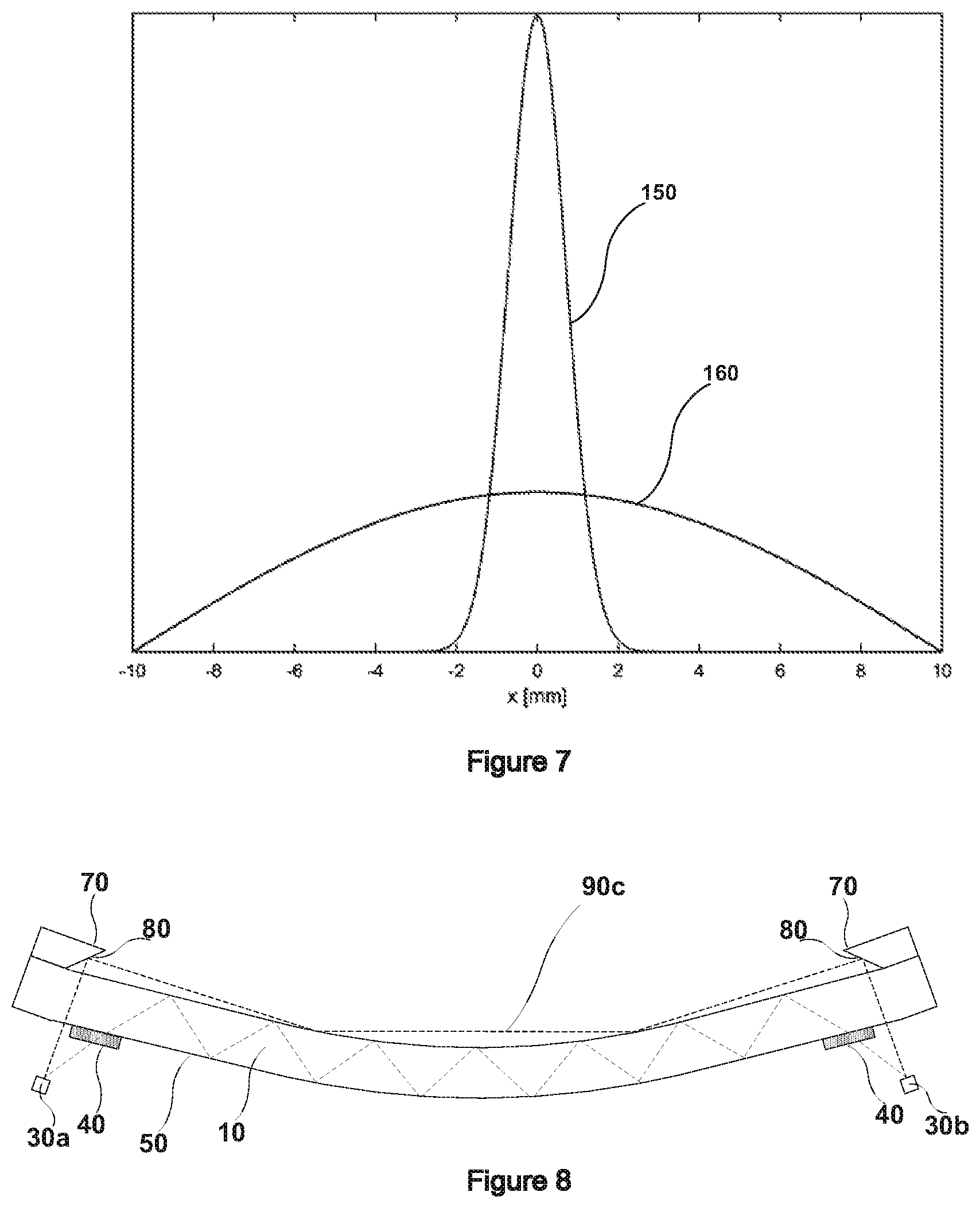
The result is that detection lines derived from light beam 90 are broader than detection lines derived from light beam 50. FIG. 5 and FIG. 6 show the difference in detection lines 95 derived from the light travelling within the glass and detection lines 96 derived from light travelling above the touch surface. In FIG. 5, detection lines 95 have a width corresponding to the short distance travelled to the in-coupling point 45 from emitters 30a. In FIG. 6, detection lines 96 have a width corresponding to the extra distance travelled to reflector surface focal point 80a from emitters 30a.
A stylus and a finger may have very large differences in size (or width as viewed from the perspective of a detection line). A stylus may typically provide a width of 2 mm to 5 mm, whereas a finger may provide a width of 5 mm to 15 mm. However, the size of a decoded touch will depend on the convolution of the detection line and the object. It is preferable to have wider detection lines above the glass, both in order to provide better cover the touch surface 20 and to get a broadened stylus interaction since this may increase the resolution. However, broadening of detection lines will reduce the ability to separate two closely spaced touch objects, potentially a key requirement for multi-touch systems.
Therefore, a solution with different detection line widths above and within the glass is required. FIG. 7 shows a signal profile of a narrow detection line overlaid on a wide detection line. Narrow detection lines 95 have a signal profile corresponding to signal profile 150 and wide detection lines 96 have a signal profile corresponding to signal profile 160.
Since a stylus will usually be used as a single touch object, broader detection lines are possible. Wide detection lines 96 with a width larger than 4 mm and possibly up to 20 mm are advantageous, although 4 mm-6 mm is preferred.
For narrow detection lines 95 designed to resolved multiple touching objects such as fingers, broadening must be kept down to a size less than or comparable to the touching objects. The width of narrow detection lines 95 is also usually limited by the width of emitters 30a and detectors 30b. Narrow detection lines 95 should be less than 5 mm in width. In a preferred embodiment, detection lines 95 are between 2 mm and 3 mm wide.
In one embodiment, reflector surface 80 is a diffusive reflecting surface. In a preferred embodiment, reflector surface 80 is a lambertian diffusive reflecting surface preferably providing a scattering of greater than 90%. Suitable materials for reflector surface 80 may include Titanium oxide paint or Microcellular foamed reflector MCPET. The advantage of using a diffusive reflecting surface is that it makes the optical system less sensitive to production, mounting and load tolerances than a specular reflector or lens. This allows the touch-sensitive apparatus 100 to be cheaper and simpler to produce. Furthermore, a diffusive reflector surface 80 also allows broader and overlapping detection lines.
The amount of light reflected by reflector surface 80 may be controlled by adjusting the size of reflector surface 80. A reflector surface 80 having a smaller surface area will reflect a small amount of light. Alternatively, paint or spray coatings may be selected to reduce the reflection, and may be applied in a specific pattern to the surface for accurate control of reflectivity.
In one embodiment, the amount of light received at each of detectors 30b via the in-glass route (shown in the figures as light beam 50) is greater than or equal to the amount of light received at each of detectors 30b via the above surface route (shown in the figures as light beam 90). In a preferred embodiment, the ratio of light received at each of detectors 30b via the in-glass route is ten times greater than the amount of light received at each of detectors 30b via the above surface route. This feature is advantageous as it allows the attenuation of the optical signal resulting from FTIR to be easily compared at the reconstruction phase to the attenuation of the optical signal resulting from occlusion of the above surface light, even though the latter is usually significantly larger than the former.
In the embodiment shown in FIG. 3, reflector surface 80 is configured to reflect a portion of light beam 90 to travel along path 90a and a portion of light beam 90 to travel along path 90b, by reflecting off touch surface 20 and coupling out to the detector. This advantageously results in a larger portion of light beam 90 being detected by detectors 30b. Furthermore, the use of path 90b allows load tolerances of the touch-sensitive apparatus 100 to be improved. A heavy load on touch surface 20 may deform the panel and bring path 90a out of alignment. However, path 90b would likely be less affected by said deformation, allowing sufficient signal to continue to be received by detectors 30b.
In an embodiment of the invention shown in FIG. 8, transmissive panel 10 is curved to form a concave surface. In this embodiment, reflector surface 80 is configured to cause a portion of light beam 90 to reflect a plurality of times off touch surface 20 to follow a path 90c shown in FIG. 8. Similarly to the above embodiment, this feature allows a further enhancement of the signal to noise ratio, even for a curved panel.
In an embodiment of the invention shown in FIG. 9, edge reflector 70 is set further back from the periphery of touch surface 20 than in the previous embodiments. The positioning of the edge reflector 70 further back from the periphery of touch surface 20 provides a longer distance from emitters 30a to reflector surface 80, allowing the above surface detection lines to be broader. Furthermore, the extra distance that the edge reflector 70 is set back provides larger overlap between wide detection lines 96 in the peripheral regions of touch surface 20 resulting in improved accuracy in areas. This is especially advantageous where narrow detection lines 95 provide limited coverage. In a preferred embodiment, the edge reflector 70 is positioned so that reflector surface 80 is set 10 mm back from in-coupling point 45.
FIG. 10 shows an embodiment of the invention featuring dust shield 110. A known problem with above-surface touch systems is the accumulation of dust and contamination around the sensor area or the area in which the light signal is emitted to travel across the touch panel. Dust or other contamination accumulating at this point will block the light signal and seriously degrade the ability of the touch system to determine a touch. For a system such as the embodiment presented in FIG. 3, the accumulation of contamination may be increased where reflector surface 80 is angled to form an overhang. This overhang forms a natural shelter for accumulating contamination, resulting in further touch signal degradation. A solution presented in FIG. 10 is that of a dust shield 110 forming a physical barrier preventing the dust from reaching reflector surface 80 and comprising transparent window 115 through which the light signal may pass unhindered. Preferably, dust shield 110 forms a sloping edge, sloping from the inside edge in contact with touch surface 20 outwardly to the top surface of edge reflector 70. This allows dust shield 110 to be effectively wiped clean.
In a preferred embodiment, transparent window 115 comprises a material of coating configured to allow only IR or Near-IR light to pass through. This feature provides improved ambient light noise reduction as light from artificial lighting or sun light is filtered before reaching detectors 30b.
In a preferred embodiment, dust shield 110 is configured with a longer dimension extending from edge reflector 70 towards touch surface 20 and with an internal top surface providing a light baffle effect so as to provide an angular filter for light entering through transparent window 115. This is advantageous for reducing ambient noise as light entering at the wrong angle is absorbed into the roof of the dust shield 110. Furthermore, when combined with the embodiment from FIG. 8, the angle of light paths travelling above the panel may be limited so that that detection lines very high above the glass 90a may be supressed.
FIG. 11 shows an alternative embodiment to the embodiment shown in FIG. 3. In FIG. 11, apparatus 100 is configured to transmit light from a first set of emitters 31a to a first set of detectors 31b inside a transmissive panel 10 so as to illuminate a touch surface 20 from within the transmissive panel 10. Apparatus 100 is also configured to transmit light from a second set of emitters 32a to a second set of detectors 32b such that the light is emitted by emitters 32a, exits transmissive panel 10 through touch surface 20 and is reflected by reflector surface 80 of edge reflector 70 to travel along path 90a in a plane parallel with touch surface 20. The light will then continue until deflected by reflector surface 80 of the edge reflector 70 at an opposing edge of the transmissive panel 10, wherein the light will be deflected back down through transmissive panel 10 and onto detectors 32b. Significant advantages may be obtained from using two separate emitting and detecting systems rather than a single set of emitters and detectors for both the above-surface and FTIR light paths. A significant problem with trying to differentiate between the attenuation of the light travelling along a path above the touch surface from the attenuation of light travelling along a path within the panel via FTIR is that a typical finger touch is likely to produce an attenuation of the light above the panel is greater than the attenuation of the light travelling within the panel via FTIR by as much as a factor of 50. This results in an attenuation signal of the light travelling in the panel which is difficult to differentiate from noise relative to the attenuation signal of the light travelling above the panel. For objects such as stylus tips, this relative difference in signal strength can be even greater. Therefore, the use of separate emitting and detecting systems for light paths above (above-surface system) and within the panel via FTIR (FTIR system) allows each system to be configured appropriately for the respective signal-to-noise ratios. The separate resulting signals can then be combined to provide a system that provides the following features:
Oil or water contamination on the touch surface may appear to the FTIR system as an attenuation surface area and generate a false touch. However, in the above embodiment, the touch output of the FTIR system may be compared to the touch output of the above-surface system to identify touches of the FTIR system which do not appear in the touch output of the above-surface system. This would indicate that the identified touches do not correspond to actual objects above the touch surface but mere contamination on the surface. The output of the identified touches can then be suppressed.
Similarly to the above, when a user raises their finger from the touch surface, a previously identified touch should be removed from the touch output. However, on occasion, finger grease from the skin is left on the touch surface and an FTIR system continues to detect and report a touch. In the above embodiment, the output of the above-surface system may be used to identify touches of the FTIR system where the touching object has now been removed. The output of the identified touches can then be suppressed.
Certain object types produce very little attenuation of the FTIR light when in contact with the touch surface e.g. Hard objects such as stylus tips. Where the above-surface system registers an object but the FTIR system does not, it can be determined that the object is likely to be a `hard object` as opposed to a normal touch from a finger. Differentiation between hard and soft surfaced objects may allow differentiation between e.g. a pen and a finger. A touch system configured to differentiate between a stylus and a finger tip may generate a different UI output in dependence on the identified object touching the touch surface.
One problem with above-surface systems is that the object touching the touch surface may completely occlude one or more light paths of the above-surface system. Where a large number of touches are simultaneously applied to the touch surface, portions of the touch surface may become significantly shielded from the light paths of the above-surface system, resulting in little or no touch signal in the shielded portion. In the above embodiment, the FTIR may continue to provide a touch signal within the occluded areas, as the attenuation of the FTIR light paths resulting from a touch is relatively small and non-occluding.
In the embodiment of FIG. 11, a first wavelength of light emitted by first set of emitters 31a and detected by first set of detectors 31b may be different to a second wavelength of light emitted by second set of emitters 32a and detected by second set of detectors 32b. This allows light to be emitted from one of the first set of emitters 31a and one of the second set of emitters 32a simultaneously and detected by the first set of detectors 31b and second set of detectors 32b without co-interference. This may also allow improved ambient light noise reduction in environments where ambient light comprises more light with a first wavelength than light with a second wavelength or vice versa. E.g. Wherein the first and second wavelengths are both near IR wavelengths.
In the embodiment of FIG. 11, the timing sequence used to activate emitters of the first and second set of emitters may be chosen to ensure that activation of the emitters of the first set of emitters does not chronologically overlap with activation of emitters of the second set of emitters. This allows potential co-interference to be minimized.
FIG. 12 shows a top plan view of the FIG. 11. In this embodiment, emitters 31a are spatially interlaced with emitters 32a around the peripheral edge of transmissive panel 10 so that emitters of first set 31a are positioned between adjacent emitters of second set 32a. Similarly, detectors 31b are spatially interlaced with detectors 32b around the peripheral edge of transmissive panel 10 so that detectors of first set 31b are positioned between adjacent emitters of second set 32b. This has the advantage of improving coverage of the touch surface where detection paths of the above-surface system cover gaps between detection paths of the FTIR system and vice versa.
In one embodiment, emitters 31a and detectors 31b are only positioned along sub-portions of the periphery of the touch surface. In this embodiment, the portion of the periphery of the touch surface along which emitters 31a and detectors 31b are positioned is smaller than the portion of the periphery of the touch surface along which emitters 31a and detectors 31b are positioned. In one example, emitters 31a and detectors 31b are only located along two opposing edges of a rectangular touch surface. In an alternative embodiment, emitters 31a are placed along one edge of the rectangular touch surface and detectors 31b are positioned along an opposing edge of the touch surface. Alternatively, emitters 31a and detectors 31b may be positioned along L-shaped portions of the periphery of the rectangular touch surface at the corners. In one embodiment, the number of emitters 31a and detectors 31b are fewer than the number of emitters 32a and detectors 32b respectively. This may result in an FTIR system with a lower resolution than the above-surface system. Alternatively, for all of the above arrangements, emitters 31a and detectors 31b may be swapped for emitters 32a and detectors 32b so that the FTIR system has a higher resolution and/or coverage than the above-surface system. These arrangements allow the advantages of a complete above-surface system or FTIR system to be supplemented with the advantages of a limited FTIR system or limited above-surface system respectively without the need for a complete version of both systems. This would allow a significant reduction in manufacturing cost, power usage, and even physical size of the touch frame. E.g. Where high accuracy pressure detection needed to be added to an above-surface system, a limited FTIR type system configured to detect pressure (as is known in the art) may be added to the above-surface system with only as many emitters and detectors needed to accurately detect pressure. In one example, the limited system comprises only 25% of the number of emitters and detectors of the complete system.
In one embodiment, a low-power mode is provided wherein only the above-surface system is powered. When a touch is detected by the above-surface system, a full-power mode is activated and power is provided to the FTIR system. This has the advantage of preserving energy during periods that the above-surface system detects no touches whilst enabling the features of the FTIR system once it is required. Alternatively, an embodiment is provided wherein only the FTIR system is powered in a low-power mode and the above-surface system is only powered on when required. This may include a system wherein the above-surface system is only activated periodically or in response to a determination that a touch detected by the FTIR system is possibly a false touch caused by contamination.
FIG. 13 shows a variation of FIG. 11 wherein emitters 31a are configured to simultaneously project light above and into transmissive panel 10 but wherein separate detectors 31b and 32b are used to provide separate above-surface and FTIR type touch signals. This advantageously allows simultaneous emission of both signals using a single emitter, allowing low energy consumption and cheaper manufacturing costs, whilst the above features.
FIG. 14 shows an alternative to FIG. 13 wherein the detectors 31b are configured to simultaneously receive light from above and from within transmissive panel 10 but wherein separate emitters 31a and 32a are used to provide separate above-surface and FTIR type touch signals. This configuration advantageously allows separate control of the light intensity of the light emitted from emitters 31a and 32a to account for environmental light noise or other situations in which light levels need to be separately altered, whilst also allowing low energy consumption and cheaper manufacturing costs.
For all of the above embodiments, alternative in-coupling and out-coupling solutions used for coupling the light into and out of transmissive panel 10 may be employed according to techniques known in the prior art. E.g. Coupling the light into the edge of the panel rather than from below.
Furthermore, alternative waveguide, lens, and reflective surface configurations to convey light from emitters 32a to a plane parallel with touch surface 20 and back to detectors 32b may be employed according to techniques known in the prior art. E.g. Configurations for conveying the light around the edge of the panel rather than through it.
REFERENCE SIGNS LIST
A. touch-sensitive apparatus 100 B. transmissive panel 10 C. touch surface 20 D. bottom surface 25 E. emitters 30a F. detectors 30b G. coupling element 40 H. in-coupling point 45 I. light beam 50 J. touching object 60 K. edge reflector 70 L. reflector surface 80 M. reflector surface focal point 80a N. light beam 90 O. path 90a P. path 90b Q. path 90c R. detection lines 95 S. detection lines 96 T. dust shield 110 U. transparent window 115 V. light paths D W. controller 120 X. signal processor 130 Y. processing unit 140 Z. signal profile 150 AA. signal profile 160
* * * * *
References
D00000
D00001
D00002
D00003
D00004
D00005
D00006
D00007
XML
uspto.report is an independent third-party trademark research tool that is not affiliated, endorsed, or sponsored by the United States Patent and Trademark Office (USPTO) or any other governmental organization. The information provided by uspto.report is based on publicly available data at the time of writing and is intended for informational purposes only.
While we strive to provide accurate and up-to-date information, we do not guarantee the accuracy, completeness, reliability, or suitability of the information displayed on this site. The use of this site is at your own risk. Any reliance you place on such information is therefore strictly at your own risk.
All official trademark data, including owner information, should be verified by visiting the official USPTO website at www.uspto.gov. This site is not intended to replace professional legal advice and should not be used as a substitute for consulting with a legal professional who is knowledgeable about trademark law.