Enclosure cooling system
Bhutta Oc
U.S. patent number 10,455,729 [Application Number 15/467,667] was granted by the patent office on 2019-10-22 for enclosure cooling system. This patent grant is currently assigned to RENO TECHNOLOGIES, INC.. The grantee listed for this patent is Reno Technologies, Inc.. Invention is credited to Imran Ahmed Bhutta.


View All Diagrams
| United States Patent | 10,455,729 |
| Bhutta | October 22, 2019 |
Enclosure cooling system
Abstract
In one embodiment, the invention can be a system for cooling an enclosure enclosing electrical components and configured to prevent air and exhaust from escaping the enclosure. The system can include a heat sink comprising a heat exchanger, and a tube extending into and out of the heat exchanger, the tube configured to transport liquid through the heat exchanger. The system can further include a fan configured to push air heated by electrical components onto the heat exchanger. The heat exchanger can be configured to receive heat from air pushed by the fan, and transfer the received heat to the liquid being transported by the tube through the heat exchanger.
| Inventors: | Bhutta; Imran Ahmed (Moorestown, NJ) | ||||||||||
|---|---|---|---|---|---|---|---|---|---|---|---|
| Applicant: |
|
||||||||||
| Assignee: | RENO TECHNOLOGIES, INC.
(Wilmington, DE) |
||||||||||
| Family ID: | 59276176 | ||||||||||
| Appl. No.: | 15/467,667 | ||||||||||
| Filed: | March 23, 2017 |
Prior Publication Data
| Document Identifier | Publication Date | |
|---|---|---|
| US 20170202106 A1 | Jul 13, 2017 | |
Related U.S. Patent Documents
| Application Number | Filing Date | Patent Number | Issue Date | ||
|---|---|---|---|---|---|
| 14982244 | Dec 29, 2015 | ||||
| 14935859 | Nov 9, 2015 | ||||
| 14622879 | Feb 15, 2015 | ||||
| 14616884 | Feb 9, 2015 | 9865432 | |||
| 14594262 | Nov 15, 2016 | 9496122 | |||
| 61925974 | Jan 10, 2014 | ||||
| 61940139 | Feb 14, 2014 | ||||
| 61940165 | Feb 14, 2014 | ||||
| 62077753 | Nov 10, 2014 | ||||
| 62097498 | Dec 29, 2014 | ||||
| 62312070 | Mar 23, 2016 | ||||
| Current U.S. Class: | 1/1 |
| Current CPC Class: | H05K 7/20218 (20130101); H01J 37/32183 (20130101); H01J 37/32522 (20130101); H03H 11/30 (20130101); H01J 37/32935 (20130101); H01J 37/3299 (20130101); H01J 37/32577 (20130101); H03H 7/38 (20130101); H01L 23/473 (20130101); H05K 7/20154 (20130101); H01L 21/67069 (20130101) |
| Current International Class: | H05K 7/20 (20060101); H03H 7/38 (20060101); H01J 37/32 (20060101); H03H 11/30 (20060101); H01L 23/473 (20060101); H01L 21/67 (20060101) |
| Field of Search: | ;261/679.47,698,702 |
References Cited [Referenced By]
U.S. Patent Documents
| 3828281 | August 1974 | Chambers |
| 4110700 | August 1978 | Rosen et al. |
| 4679007 | July 1987 | Reese et al. |
| 4692643 | September 1987 | Tokunaga et al. |
| 4751408 | June 1988 | Rambert |
| 4929855 | May 1990 | Ezzeddine |
| 5012123 | April 1991 | Ayasli et al. |
| 5079507 | January 1992 | Ishida et al. |
| 5285347 | February 1994 | Fox et al. |
| 5394936 | March 1995 | Budelman |
| 5654679 | August 1997 | Mavretic et al. |
| 5706668 | January 1998 | Hilpert |
| 5815047 | September 1998 | Sorensen et al. |
| 5823248 | October 1998 | Kadota |
| 5849136 | December 1998 | Mintz et al. |
| 5880921 | March 1999 | Tham et al. |
| 5889252 | March 1999 | Williams et al. |
| 5971591 | October 1999 | Vona et al. |
| 6046641 | April 2000 | Chawla et al. |
| 6137367 | October 2000 | Ezzedine et al. |
| 6208510 | March 2001 | Trudeau |
| 6252354 | June 2001 | Collins et al. |
| 6343478 | February 2002 | Chang |
| 6400012 | June 2002 | Miller et al. |
| 6424232 | July 2002 | Mavretic et al. |
| 6583572 | June 2003 | Veltrop et al. |
| 6621372 | September 2003 | Kondo et al. |
| 6657395 | December 2003 | Windhorn |
| 6677828 | January 2004 | Harnett et al. |
| 6703080 | March 2004 | Reyzelman et al. |
| 6791274 | September 2004 | Hauer et al. |
| 6794951 | September 2004 | Finley |
| 6818562 | November 2004 | Todorow et al. |
| 6888313 | May 2005 | Blackburn et al. |
| 6888396 | May 2005 | Hajimiri et al. |
| 6946847 | September 2005 | Nishimori et al. |
| 6967547 | November 2005 | Pellegrini et al. |
| 6995545 | February 2006 | Tracy |
| 7002799 | February 2006 | Malone et al. |
| 7004107 | February 2006 | Raoux et al. |
| RE39051 | March 2006 | Harnett |
| 7071786 | July 2006 | Inoue et al. |
| 7095178 | August 2006 | Nakano et al. |
| 7113761 | September 2006 | Bickham et al. |
| 7122965 | October 2006 | Goodman |
| 7164236 | January 2007 | Mitrovic et al. |
| 7199678 | April 2007 | Matsuno |
| 7212403 | May 2007 | Rockenfeller |
| 7251121 | July 2007 | Bhutta |
| 7298091 | November 2007 | Pickard et al. |
| 7298128 | November 2007 | Bhutta |
| 7304438 | December 2007 | Kishinevsky |
| 7332981 | February 2008 | Matsuno |
| 7342789 | March 2008 | Hall et al. |
| 7439610 | October 2008 | Weigand |
| 7480571 | January 2009 | Howald et al. |
| 7495524 | February 2009 | Omae et al. |
| 7498908 | March 2009 | Gurov |
| 7514935 | April 2009 | Pankratz |
| 7518466 | April 2009 | Sorensen et al. |
| 7535312 | May 2009 | McKinzie, III |
| 7602127 | October 2009 | Coumou |
| 7642879 | January 2010 | Matsuno |
| 7666464 | February 2010 | Collins et al. |
| 7701714 | April 2010 | Shabany |
| 7714676 | May 2010 | McKinzie, III |
| 7728602 | June 2010 | Valcore et al. |
| 7745955 | June 2010 | Kirchmeier et al. |
| 7755300 | July 2010 | Kishinevsky et al. |
| 7764140 | July 2010 | Nagarkatti et al. |
| 7777567 | August 2010 | Polizze |
| 7819175 | October 2010 | Zoodsma |
| 7852170 | December 2010 | McKinzie, III |
| 7863996 | January 2011 | Cotter et al. |
| 7868556 | January 2011 | Xia |
| 7872523 | January 2011 | Sivakumar et al. |
| 7917104 | March 2011 | Manssen et al. |
| 7969096 | June 2011 | Chen |
| 8008982 | August 2011 | McKinzie, III |
| 8040068 | October 2011 | Coumou et al. |
| RE42917 | November 2011 | Hauer et al. |
| 8089026 | January 2012 | Sellers |
| 8102954 | January 2012 | Coumou |
| 8110991 | February 2012 | Coumou |
| 8203859 | June 2012 | Omae et al. |
| 8217731 | July 2012 | McKinzie, III |
| 8217732 | July 2012 | McKinzie, III |
| 8228112 | July 2012 | Reynolds |
| 8237501 | August 2012 | Owen |
| 8264154 | September 2012 | Banner et al. |
| 8278909 | October 2012 | Fletcher |
| 8289029 | October 2012 | Coumou |
| 8299867 | October 2012 | McKinzie, III |
| 8314561 | November 2012 | Fisk et al. |
| 8330432 | December 2012 | Van Zyl et al. |
| 8334657 | December 2012 | Xia |
| 8334700 | December 2012 | Coumou et al. |
| 8335479 | December 2012 | Koya et al. |
| 8344559 | January 2013 | Van Zyl et al. |
| 8344801 | January 2013 | Owen et al. |
| 8368308 | February 2013 | Banna et al. |
| 8368469 | February 2013 | Mohammadi et al. |
| 8395322 | March 2013 | Coumou |
| 8416008 | April 2013 | Van Zyl et al. |
| 8436643 | May 2013 | Mason |
| 8461842 | June 2013 | Thuringer et al. |
| 8466736 | June 2013 | Reynolds |
| 8487706 | July 2013 | Li et al. |
| 8502689 | August 2013 | Chen et al. |
| 8513889 | August 2013 | Zhang et al. |
| 8520413 | August 2013 | Tran et al. |
| 8536636 | September 2013 | Englekirk |
| 8552665 | October 2013 | Larson et al. |
| 8558633 | October 2013 | McKinzie, III |
| 8559907 | October 2013 | Burgener et al. |
| 8564381 | October 2013 | McKinzie |
| 8569842 | October 2013 | Weis et al. |
| 8576010 | November 2013 | Yanduru |
| 8576013 | November 2013 | Coumou |
| 8587321 | November 2013 | Chen et al. |
| 8620236 | December 2013 | Manssen et al. |
| 8624501 | January 2014 | Nagarkatti et al. |
| 8633782 | January 2014 | Nagarkatti et al. |
| 8638159 | January 2014 | Ranta et al. |
| 8649754 | February 2014 | Burgener et al. |
| 8659335 | February 2014 | Nagarkatti et al. |
| 8674606 | March 2014 | Carter et al. |
| 8680928 | March 2014 | Jeon et al. |
| 8686796 | April 2014 | Presti |
| 8710926 | April 2014 | Nagarkatti et al. |
| 8716984 | May 2014 | Mueller et al. |
| 8723423 | May 2014 | Hoffman et al. |
| 8742669 | June 2014 | Carter et al. |
| 8773019 | July 2014 | Coumou et al. |
| 8779859 | July 2014 | Su et al. |
| 8781415 | July 2014 | Coumou et al. |
| 8815329 | August 2014 | Ilic et al. |
| 8847561 | September 2014 | Karlieek et al. |
| 8884180 | November 2014 | Ilic et al. |
| 8884525 | November 2014 | Hoffman et al. |
| 8890537 | November 2014 | Valcore, Jr. et al. |
| 8912835 | December 2014 | Nagarkatti et al. |
| 8928329 | January 2015 | Downing et al. |
| 9083343 | July 2015 | Li et al. |
| 9190993 | November 2015 | Li |
| 9306533 | April 2016 | Anton |
| 2002/0060914 | May 2002 | Porter et al. |
| 2003/0007372 | January 2003 | Porter et al. |
| 2003/0046013 | March 2003 | Gerrish |
| 2004/0100770 | May 2004 | Chu et al. |
| 2005/0201055 | September 2005 | Jyo |
| 2005/0213306 | September 2005 | Vos |
| 2006/0170367 | August 2006 | Bhutta |
| 2006/0198077 | September 2006 | Bhutta |
| 2006/0232471 | October 2006 | Coumou |
| 2007/0075784 | April 2007 | Pettersson et al. |
| 2007/0139122 | June 2007 | Nagarkatti et al. |
| 2007/0227699 | October 2007 | Nishi |
| 2007/0285894 | December 2007 | Hatamian et al. |
| 2008/0173427 | July 2008 | Schumacher |
| 2008/0179948 | July 2008 | Nagarkatti et al. |
| 2008/0180179 | July 2008 | Polizzo |
| 2008/0197854 | August 2008 | Valcore et al. |
| 2009/0207537 | August 2009 | Coumou |
| 2009/0229794 | September 2009 | Schon |
| 2010/0001796 | January 2010 | Sivakumar et al. |
| 2010/0073104 | March 2010 | Cotter et al. |
| 2010/0123502 | May 2010 | Bhutta et al. |
| 2010/0128431 | May 2010 | Eriksen et al. |
| 2010/0194195 | August 2010 | Coumou et al. |
| 2010/0201370 | August 2010 | Coumou et al. |
| 2010/0231296 | September 2010 | Nagarkatti et al. |
| 2011/0241781 | October 2011 | Owen et al. |
| 2011/0247696 | October 2011 | Zolock et al. |
| 2012/0013253 | January 2012 | Coumou |
| 2012/0062322 | March 2012 | Owen |
| 2012/0188007 | July 2012 | Van Zyl et al. |
| 2012/0262064 | October 2012 | Nagarkatti et al. |
| 2013/0043854 | February 2013 | Tran et al. |
| 2013/0169359 | July 2013 | Coumou |
| 2013/0193867 | August 2013 | Van Zyl et al. |
| 2013/0206367 | August 2013 | Chen et al. |
| 2013/0207738 | August 2013 | Mason |
| 2013/0222055 | August 2013 | Coumou et al. |
| 2013/0257311 | October 2013 | Tran et al. |
| 2013/0314163 | November 2013 | Costa |
| 2013/0320853 | December 2013 | Carter et al. |
| 2014/0009248 | January 2014 | Granger-Jones |
| 2014/0028389 | January 2014 | Coumou |
| 2014/0028398 | January 2014 | Owen |
| 2014/0049250 | February 2014 | Brown et al. |
| 2014/0055034 | February 2014 | Coumou |
| 2014/0061156 | March 2014 | Brouk et al. |
| 2014/0062303 | March 2014 | Hoffman et al. |
| 2014/0097908 | April 2014 | Fisk, II et al. |
| 2014/0117861 | May 2014 | Finley et al. |
| 2014/0117872 | May 2014 | Finley |
| 2014/0118031 | May 2014 | Rughoonundon et al. |
| 2014/0210345 | July 2014 | Hoffman |
| 2014/0210551 | July 2014 | Mueller |
| 2014/0218076 | August 2014 | Coumou et al. |
| 2014/0220913 | August 2014 | Coumou et al. |
| 2014/0231243 | August 2014 | Finley |
| 2014/0232266 | August 2014 | Finley et al. |
| 2014/0266492 | September 2014 | Radomski et al. |
| 2014/0306742 | October 2014 | Menzer et al. |
| 2014/0320013 | October 2014 | Coumou et al. |
| 2015/0115289 | April 2015 | Fursin et al. |
| 2015/0138722 | May 2015 | French, Jr. |
| 102297538 | Dec 2011 | CN | |||
| 103629851 | Dec 2011 | CN | |||
| 0840349 | May 1998 | EP | |||
| 0840350 | May 1998 | EP | |||
| 2000036554 | Feb 2000 | JP | |||
| 2006096589 | Sep 2006 | WO | |||
| 2008118342 | Oct 2008 | WO | |||
Attorney, Agent or Firm: The Belles Group, P.C.
Parent Case Text
CROSS REFERENCE TO RELATED APPLICATIONS
The present application is a continuation in part of U.S. patent application Ser. No. 14/982,244, filed Dec. 29, 2015, which is a continuation in part of U.S. patent application Ser. No. 14/935,859, filed Nov. 9, 2015, which is a continuation in part of U.S. patent application Ser. No. 14/622,879, filed Feb. 15, 2015, which is a continuation in part of U.S. patent application Ser. No. 14/616,884, filed Feb. 9, 2015, which is a continuation in part of U.S. patent application Ser. No. 14/594,262, filed Jan. 12, 2015, now U.S. Pat. No. 9,496,122, which in turn claims priority to U.S. Provisional Patent Application No. 61/925,974, filed Jan. 10, 2014. U.S. patent application Ser. No. 14/616,884 also claims priority to U.S. Provisional Patent Application No. 61/940,139, filed Feb. 14, 2014. U.S. patent application Ser. No. 14/622,879 also claims priority to U.S. Provisional Patent Application No. 61/940,165, filed Feb. 14, 2014. U.S. patent application Ser. No. 14/935,859, filed Nov. 9, 2015, also claims the benefit of U.S. Provisional Patent Application No. 62/077,753, filed Nov. 10, 2014. U.S. patent application Ser. No. 14/982,244, filed Dec. 29, 2015, also claims priority to U.S. Provisional Patent Application No. 62/097,498, filed Dec. 29, 2014. The present application also claims the benefit of U.S. Provisional Patent Application No. 62/312,070 filed on Mar. 23, 2016. The disclosures of these references are incorporated herein by reference in their entireties.
Claims
What is claimed is:
1. A system comprising: an enclosure enclosing electrical components and configured to prevent air within the enclosure and exhaust from the electrical components from escaping the enclosure; a heat sink at least partially within the enclosure, the heat sink comprising: a main housing within the enclosure, the main housing having a flat and thermally conductive main housing surface for laying against an electrical component shelf surface or for receiving electrical components directly thereon; thermally conductive fins positioned alongside each other, adjacent to the main housing, and within the enclosure; and a tube extending into and out of each of the main housing and the fins to transport liquid through both the main housing and the fins; and a fan enclosed by the enclosure, the fan configured to push air heated by electrical components onto the fins; wherein the fins are configured to receive a first heat from air pushed by the fan, and transfer the received first heat to the liquid being transported by the tube through the fins; wherein the main housing is configured to receive a second heat from the electrical components on the thermally conductive main housing surface and transfer the received second heat to the liquid being transported by the tube; wherein the main housing further comprises a first edge and a second edge opposite the first edge; wherein the fins further comprise a first edge and a second edge opposite the first edge, the main housing second edge being adjacent the fins first edge; wherein the tube enters the main housing at the main housing first edge; wherein the tube enters the fins at the fins first edge; wherein the tube exits the fins at the fins first edge; and wherein the tube exits the main housing at the main housing first edge.
2. The system of claim 1 wherein the electrical components form part of a system for manufacturing semiconductors.
3. The system of claim 1 wherein the fan is mounted on the heat sink.
4. The system of claim 1 wherein the main housing second edge is in contact with the fins first edge.
5. A method of cooling an enclosure enclosing electrical components and configured to prevent air within the enclosure and exhaust from the electrical components from escaping the enclosure, the method comprising: positioning a heat sink at least partially within the enclosure, the heat sink comprising: a main housing within the enclosure, the main housing having a flat and thermally conductive main housing surface for laying against an electrical component shelf surface or for receiving electrical components directly thereon; thermally conductive fins positioned alongside each other, adjacent to the main housing, and within the enclosure; and a tube extending into and out of each of the main housing and the fins to transport liquid through both the main housing and the fins; a fan enclosed by the enclosure configured to push air heated by electrical components onto the fins; receiving, at the fins, a first heat from the pushed air; transferring, by the fins, the received first heat to liquid being transported by the tube through the fins; and receiving, by the main housing, a second heat from the electrical components on the thermally conductive main housing surface, and transferring the received second heat to the liquid being transported by the tube; wherein the main housing further comprises a first edge and a second edge opposite the first edge; wherein the fins further comprise a first edge and a second edge opposite the first edge, the main housing second edge being adjacent the fins first edge; wherein the tube enters the main housing at the main housing first edge; wherein the tube enters the fins at the fins first edge; wherein the tube exits the fins at the fins first edge; and wherein the tube exits the main housing at the main housing first edge.
6. The method of claim 5 wherein the electrical components form part of a system for manufacturing semiconductors.
7. The method of claim 5 wherein the electrical components form part of an RF generator or an RF matching network.
8. The method of claim 7 further comprising, upon receipt of a fault signal, removing power from inputs of the RF generator or the RF matching network.
9. The method of claim 7 further comprising, upon receipt of a fault signal, opening a system interlock.
10. The method of claim 5 wherein the fan is mounted on the heat sink.
11. The method of claim 5 wherein the main housing and fins are located side-by-side and contact each other along at least one edge.
12. The method of claim 5 wherein the tube extends along a first side of the main housing and a second side of the main housing opposite the first side.
13. A method of manufacturing a semiconductor, the method comprising: operably coupling a matching network between an RF source and a plasma chamber, wherein the plasma chamber is configured to deposit a material layer onto the substrate or etch a material layer from the substrate, and electrical components of the RF source or the matching network are enclosed by an enclosure that is configured to prevent air within the enclosure and exhaust from the electrical components from escaping the enclosure; positioning a heat sink at least partially within the enclosure, the heat sink comprising: a main housing within the enclosure, the main housing having a flat and thermally conductive main housing surface for laying against an electrical component shelf surface or for receiving electrical components directly thereon; thermally conductive fins positioned alongside each other, adjacent to the main housing, and within the enclosure; and a tube extending into and out of each of the main housing and the fins to transport liquid through both the main housing and the fins; placing a substrate in the plasma chamber; energizing plasma within the plasma chamber by coupling RF power from the RF source into the plasma chamber to perform a deposition or etching; a fan enclosed by the enclosure, pushing air heated by electrical components onto the fins; receiving, at the fins, a first heat from the pushed air; and transferring, by the fins, the received first heat to liquid being transported by the tube through the fins; and receiving, by the main housing, a second heat from the electrical components on the thermally conductive main housing surface, and transferring the received second heat to the liquid being transported by the tube; wherein the main housing further comprises a first edge and a second edge opposite the first edge; wherein the fins further comprise a first edge and a second edge opposite the first edge, the main housing second edge being adjacent the fins first edge; wherein the tube enters the main housing at the main housing first edge; wherein the tube enters the fins at the fins first edge; wherein the tube exits the fins at the fins first edge; and wherein the tube exits the main housing at the main housing first edge.
14. A heat sink comprising: a main housing within an enclosure, the main housing having a flat and thermally conductive main housing surface for laying against an electrical component shelf surface or for receiving electrical components directly thereon; thermally conductive fins positioned alongside each other, adjacent to the main housing, and within an enclosure; and a tube extending into and out of each of the main housing and the fins to transport liquid through both the main housing and the fins; wherein the fins are configured to receive a first heat from air heated by electrical components, and transfer the received heat to the liquid being transported by the tube through the fins; and wherein the main housing is configured to receive a second heat from the electrical components on the thermally conductive main housing surface and transfer the received second heat to the liquid being transported by the tube; wherein the main housing further comprises a first edge and a second edge opposite the first edge; wherein the fins further comprise a first edge and a second edge opposite the first edge, the main housing second edge being adjacent the fins first edge; wherein the tube enters the main housing at the main housing first edge; wherein the tube enters the fins at the fins first edge; wherein the tube exits the fins at the fins first edge; and wherein the tube exits the main housing at the main housing first edge.
15. A semiconductor processing tool comprising: a plasma chamber configured to deposit a material onto a substrate or etch a material from the substrate; an impedance matching circuit operably coupled to the plasma chamber; and an enclosure enclosing electrical components of the matching circuit, the enclosure configured to prevent air within the enclosure and exhaust from the electrical components from escaping the enclosure; a heat sink at least partially within the enclosure, the heat sink comprising: a main housing within the enclosure; thermally conductive fins positioned alongside each other, adjacent to the main housing, and within the enclosure; and a tube extending into and out of each of the fins to transport liquid through both the main housing and the fins; and a fan enclosed by the enclosure, the fan configured to push air heated by electrical components onto the fins; wherein the fins are configured to receive heat from air pushed by the fan, and transfer the received heat to the liquid being transported by the tube through the fins; wherein the main housing further comprises a first edge and a second edge opposite the first edge; wherein the fins further comprise a first edge and a second edge opposite the first edge, the main housing second edge being adjacent the fins first edge; wherein the tube enters the main housing at the main housing first edge; wherein the tube enters the fins at the fins first edge; wherein the tube exits the fins at the fins first edge; and wherein the tube exits the main housing at the main housing first edge.
Description
BACKGROUND
Radio Frequency (RF) amplifiers, generators and matching networks are used in many applications, including telecommunication, broadcast, and industrial processing. These systems and their components can generate heat that can compromise system operation. Thus, there is a need to cool such systems.
In an RF generator, for example, an RF signal is taken at the input of the RF amplifier and this RF signal is used to modulate the power derived from the DC power supply in order to provide RF power at significantly higher power than the input. The difference between the RF output power and the DC input power is the loss within the RF generator. This loss is then dissipated as heat among the different components of the RF generator. A fan can circulate air from the outside of the RF housing into the housing and over the circuits and then purge the air from holes in the sides of the housing. For higher power RF generators, one could use a water-cooled heat sink that is situated adjacent to the power Field Effect Transistors (FET) to remove heat generated in their components. Some of the electrical circuits, however, are not mounted on the heat sink and therefore must be cooled by other means, such as air circulation that requires the use of fans in addition to the use of a water-cooled heat sink.
Similarly, for an RF matching network, the internal resistances of the components result in varying levels of heat generation in those components. Certain components may be cooled efficiently when they are mounted to a heat sink while other components can only be cooled through air flowing over those components. The heat sink in an RF matching network may be either air cooled or water cooled.
In a semiconductor manufacturing system, an RF generator delivers power to a vacuum chamber, through an RF matching network, to create a plasma. While the RF generator has internal protection circuitry that can reduce the output power or completely shut off the power if a fault occurs in the system, sometimes the reaction to a fault is not fast enough and can result in a component failure. A component's failure can result in thermal damage to the component as well as the PCB assembly or other assemblies to which it is mounted. This thermal damage can result in scorching of the component or other assemblies resulting in outgassing of material from those assemblies. If the RF generator is air cooled and has an air inlet and exhaust holes in its enclosure, the outgassed gasses and material can be ejected from the RF generator and contaminate the surrounding environment. Contamination of the surrounding environment can in turn contaminate wafers or substrates in the semiconductor fabrication plant (fab) resulting in extensive financial damage to the fab. A similar situation can result from failure of a component or assembly in an air-cooled RF matching network.
For these reasons, it is important to prevent the outgassing of gasses and material from an RF generator or an RF matching network or a combination an RF generator and an RF matching network. Additionally, to limit further damage to the RF generator and or the RF matching network, a need exists to limit or prevent further power from being dissipated into the failed component. Thus, there exists a need for an effective method for cooling enclosed systems, such as systems utilizing large power generators.
BRIEF SUMMARY
The present disclosure may be directed, in one aspect, to a system including an enclosure enclosing electrical components and configured to prevent air and exhaust from escaping the enclosure; a heat sink at least partially within the enclosure, the heat sink comprising a heat exchanger; and a tube extending into and out of the heat exchanger, the tube configured to transport liquid through the heat exchanger; and a fan enclosed by the enclosure, the fan configured to push air heated by electrical components onto the heat exchanger; wherein the heat exchanger is configured to receive heat from air pushed by the fan, and transfer the received heat to the liquid being transported by the tube through the heat exchanger.
In another aspect, a method of cooling an enclosure enclosing electrical components and configured to prevent air and exhaust from escaping the enclosure includes positioning a heat sink at least partially within the enclosure, the heat sink comprising a heat exchanger; and a tube extending into and out of the heat exchanger, the tube configured to transport liquid through the heat exchanger; by a fan enclosed by the enclosure, pushing air heated by electrical components onto the heat exchanger; receiving, at the heat exchanger, heat from the pushed air; and transferring, by the heat exchanger, the received heat to liquid being transported by the tube through the heat exchanger.
In yet another aspect, a method of manufacturing a semiconductor includes operably coupling a matching network between an RF source and a plasma chamber, wherein the plasma chamber is configured to deposit a material layer onto the substrate or etch a material layer from the substrate, and electrical components of the RF source or the matching network are enclosed by an enclosure that is configured to prevent air and exhaust from escaping the enclosure; positioning a heat sink at least partially within the enclosure, the heat sink comprising a heat exchanger and a tube extending into and out of the heat exchanger, the tube configured to transport liquid through the heat exchanger; placing a substrate in the plasma chamber; energizing plasma within the plasma chamber by coupling RF power from the RF source into the plasma chamber to perform a deposition or etching; by a fan enclosed by the enclosure, pushing air heated by electrical components onto the heat exchanger; receiving, at the heat exchanger, heat from the pushed air; and transferring, by the heat exchanger, the received heat to liquid being transported by the tube through the heat exchanger.
In yet another aspect, a heat sink includes a heat exchanger; and a tube extending into and out of the heat exchanger, the tube configured to transport liquid through the heat exchanger; wherein heat exchanger is configured to receive heat from air heated by electrical components, and transfer the received heat to the liquid being transported by the tube through the heat exchanger.
BRIEF DESCRIPTION OF THE DRAWINGS
The present disclosure will become more fully understood from the detailed description and the accompanying drawings, wherein:
FIG. 1 is a schematic representation of an embodiment of an RF impedance matching network using EVCs incorporated into a semiconductor wafer fabrication system;
FIG. 2A illustrates an EVC for use in an RF impedance matching network;
FIG. 2B is a schematic representation of an embodiment of an electronic circuit for providing a variable capacitance.
FIG. 2C is a schematic representation of an embodiment of an EVC having three capacitor arrays.
FIG. 3 illustrates a first switching circuit for use with an EVC;
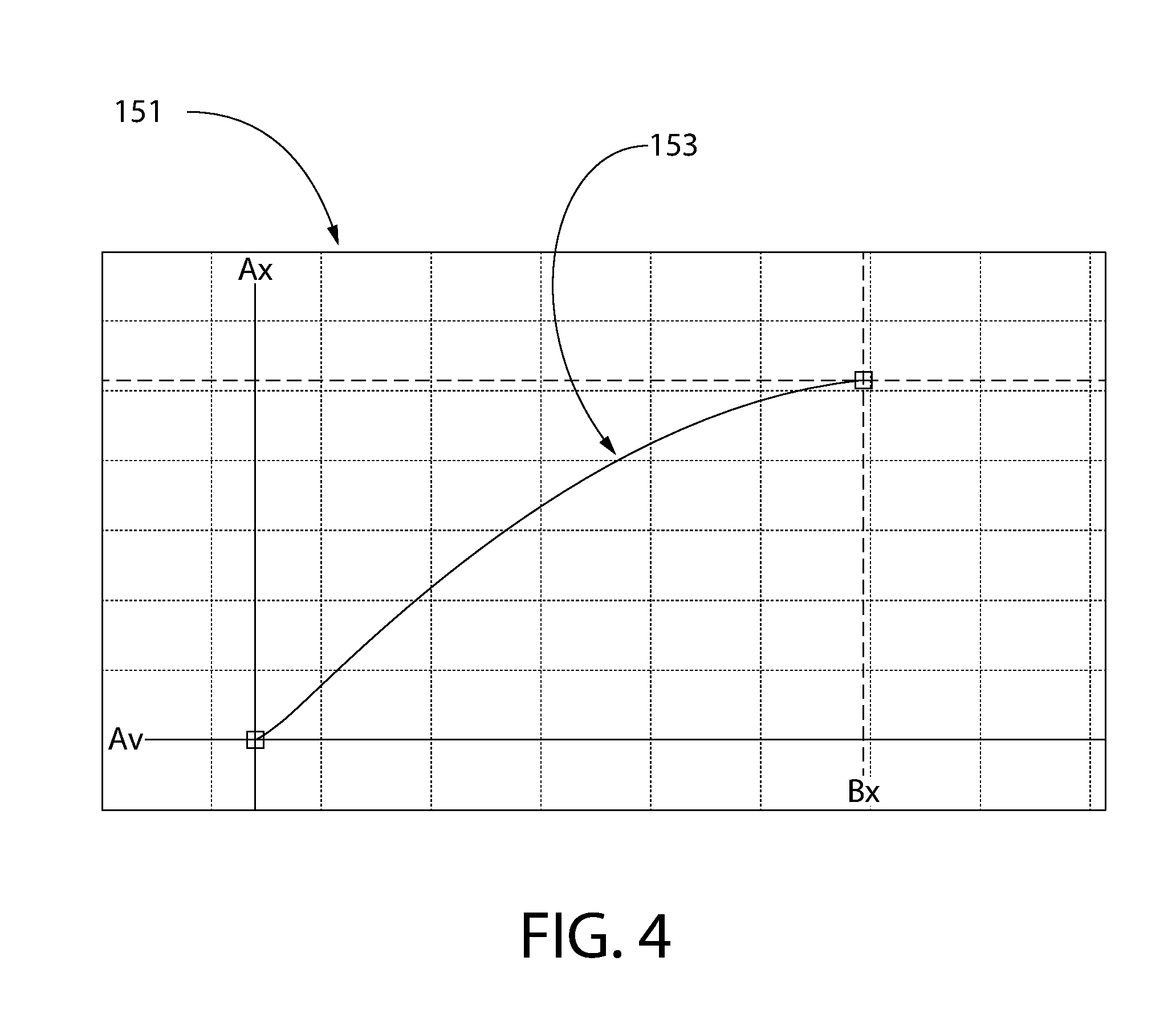
FIG. 4 is a graphical representation showing the timing capabilities of a driver circuit to switch to high voltage on the common output;
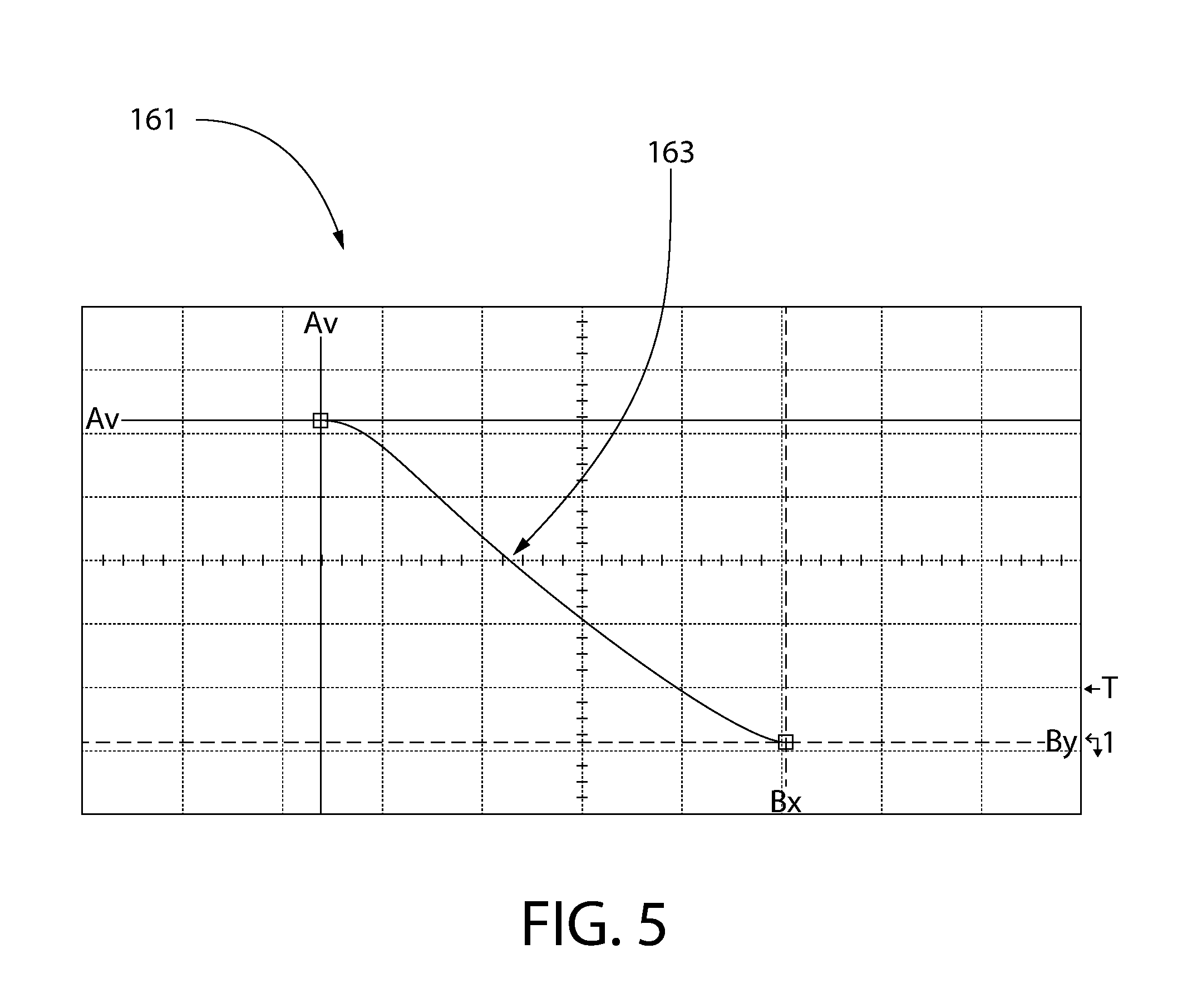
FIG. 5 is a graphical representation showing the timing capabilities of a driver circuit to switch to low voltage on the common output;
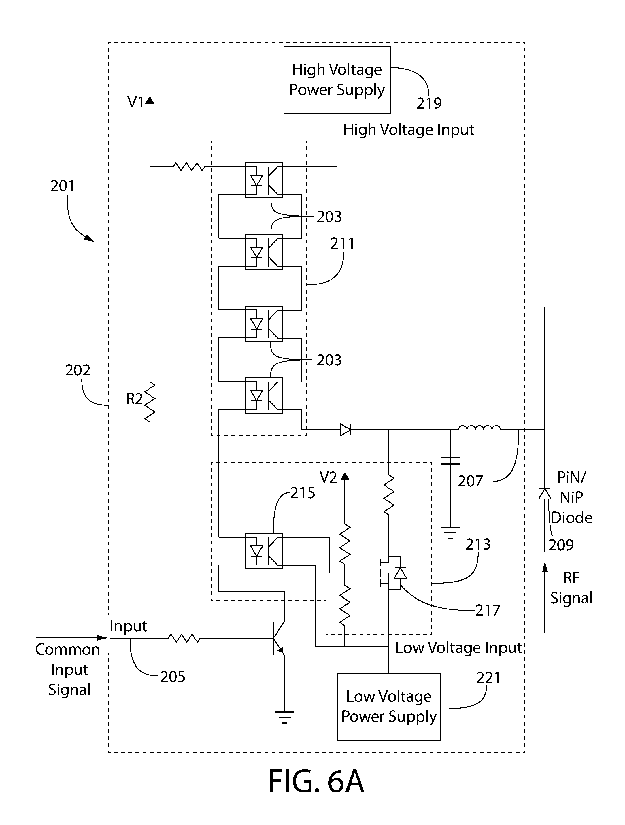
FIG. 6A illustrates a second switching circuit for use with an EVC;
FIG. 6B illustrates a third switching circuit for use with an EVC;
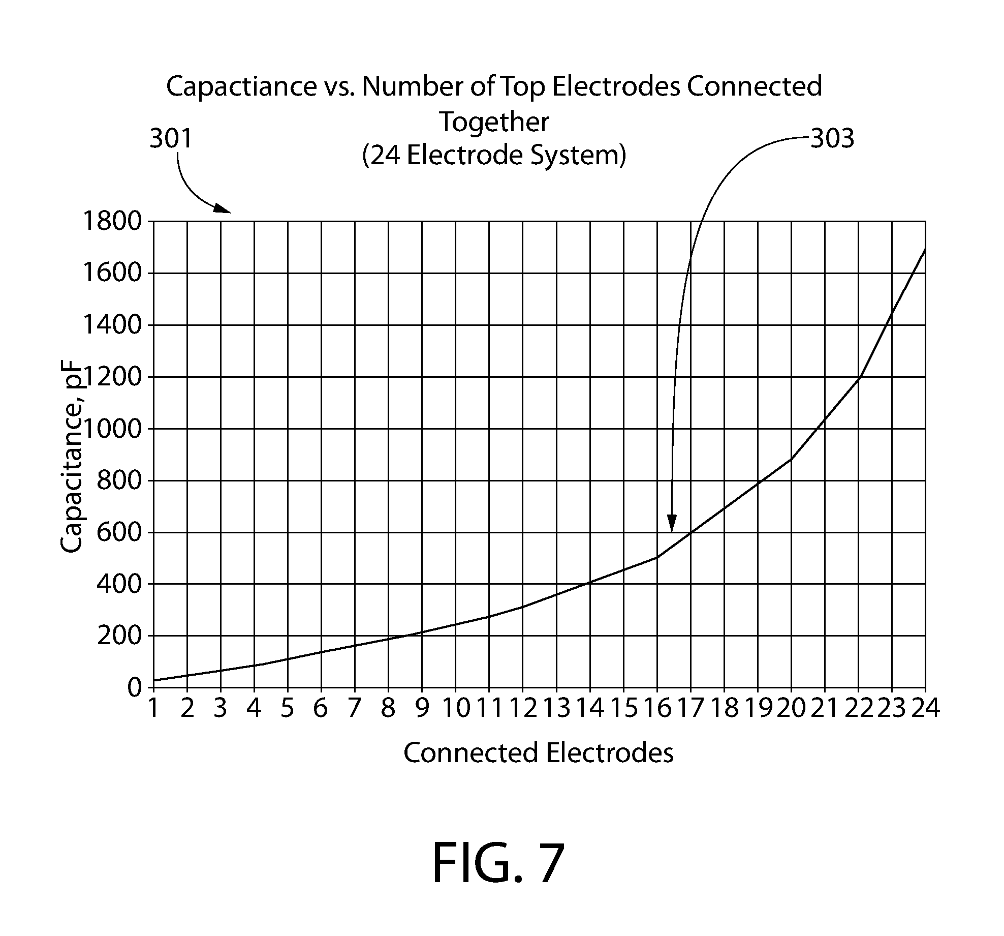
FIG. 7 is a graph showing the capacitance range of an EVC;
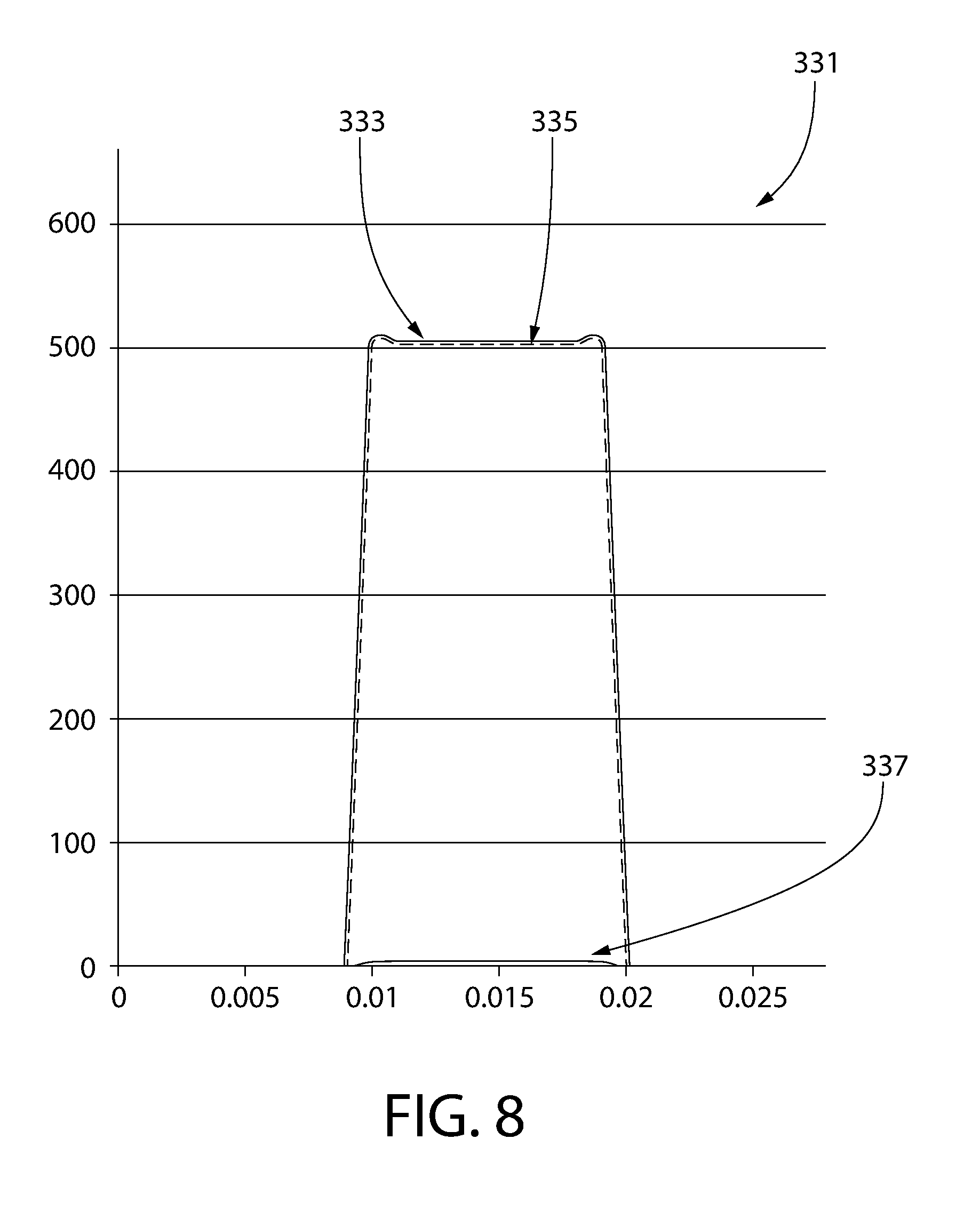
FIG. 8 is a graph showing the stable delivered power and the low reflected power that an impedance matching network including EVCs may provide during tuning;
FIG. 9 is a graphical representation showing the reflected RF power profile through an RF impedance matching network using EVCs and showing the voltage supplied to the driver circuit for the EVCs; and
FIG. 10 is a flow chart showing an embodiment of a process for matching an impedance.
FIG. 11 shows a cooling system according to one embodiment.
FIGS. 12-14 show views of a heat sink according to one embodiment.
FIG. 15 is a flow chart for a method of cooling an enclosure according to one embodiment.
DETAILED DESCRIPTION
The following description of the preferred embodiment(s) is merely exemplary in nature and is in no way intended to limit the invention or inventions. The description of illustrative embodiments is intended to be read in connection with the accompanying drawings, which are to be considered part of the entire written description. In the description of the exemplary embodiments disclosed herein, any reference to direction or orientation is merely intended for convenience of description and is not intended in any way to limit the scope of the present invention. Relative terms such as "lower," "upper," "horizontal," "vertical," "above," "below," "up," "down," "left," "right," "top," "bottom," "front" and "rear" as well as derivatives thereof (e.g., "horizontally," "downwardly," "upwardly," etc.) should be construed to refer to the orientation as then described or as shown in the drawing under discussion. These relative terms are for convenience of description only and do not require that the apparatus be constructed or operated in a particular orientation unless explicitly indicated as such. Terms such as "attached," "affixed," "connected," "coupled," "interconnected," "secured" and other similar terms refer to a relationship wherein structures are secured or attached to one another either directly or indirectly through intervening structures, as well as both movable or rigid attachments or relationships, unless expressly described otherwise. The discussion herein describes and illustrates some possible non-limiting combinations of features that may exist alone or in other combinations of features. Furthermore, as used herein, the term "or" is to be interpreted as a logical operator that results in true whenever one or more of its operands are true. Furthermore, as used herein, the phrase "based on" is to be interpreted as meaning "based at least in part on," and therefore is not limited to an interpretation of "based entirely on."
As used throughout, ranges are used as shorthand for describing each and every value that is within the range. Any value within the range can be selected as the terminus of the range. In addition, all references cited herein are hereby incorporated by referenced in their entireties. In the event of a conflict in a definition in the present disclosure and that of a cited reference, the present disclosure controls.
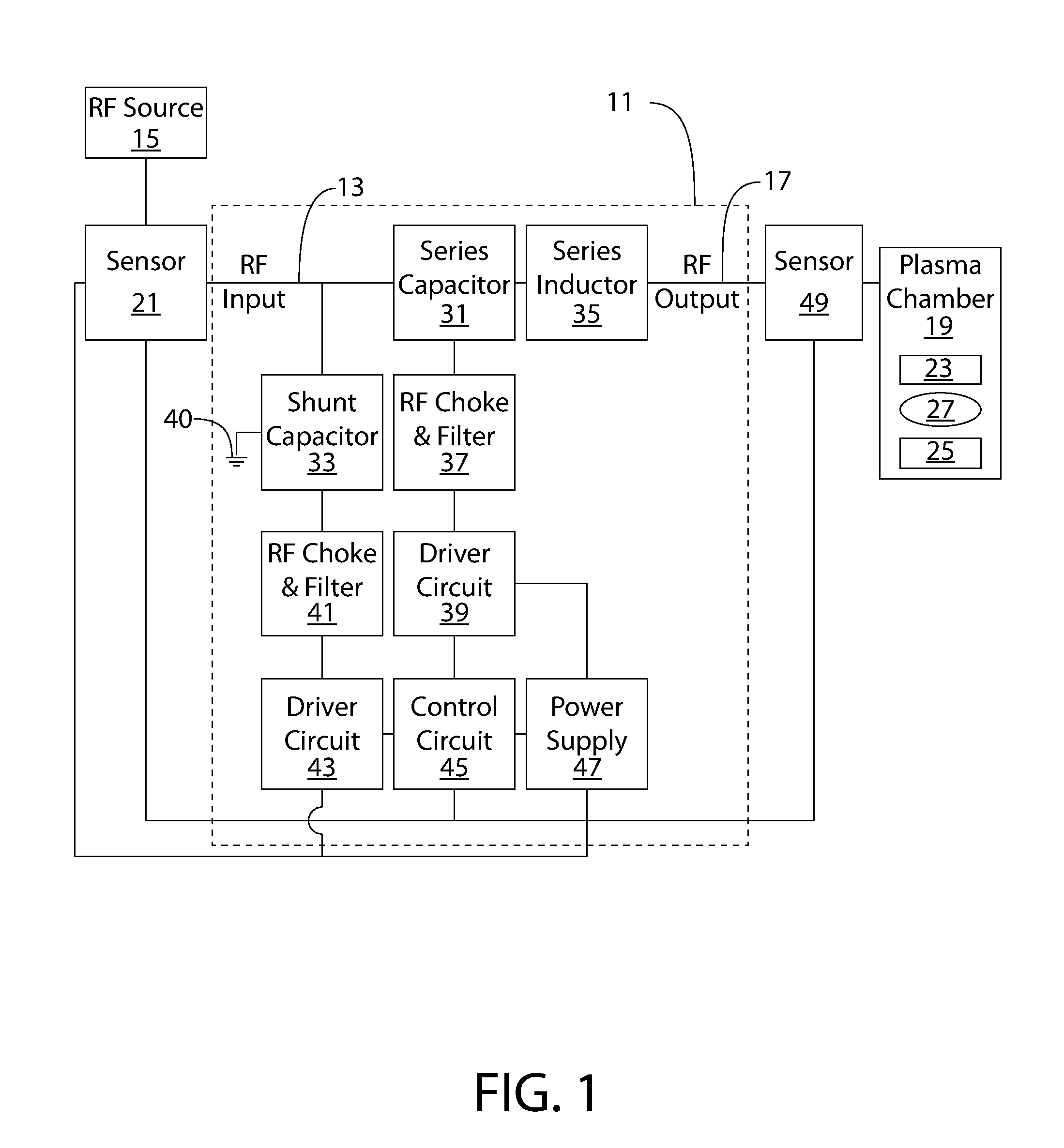
Turning in detail to the drawings, FIG. 1 illustrates an RF impedance matching network 11 having an RF input 13 connected to an RF source 15 and an RF output 17 connected to a plasma chamber 19. An RF input sensor 21 is connected between the RF impedance matching network 11 and the RF source 15 so that the RF signal output from the RF source 15 may be monitored. An RF output sensor 49 is connected between the RF impedance matching network 11 and the plasma chamber 19 so that the RF output from the impedance matching network, and the plasma impedance presented by the plasma chamber 19, may be monitored. Certain embodiments may include only one of the input sensor 21 and the output sensor 49. The functioning of these sensors 21, 49 are described in greater detail below.
The RF impedance matching network 11 serves to help maximize the amount of RF power transferred from the RF source 15 to the plasma chamber 19 by matching the impedance at the RF input 13 to the fixed impedance of the RF source 15. The matching network 11 can consist of a single module within a single housing designed for electrical connection to the RF source 15 and plasma chamber 19. In other embodiments, the components of the matching network 11 can be located in different housings, some components can be outside of the housing, and/or some components can share a housing with a component outside the matching network.
As is known in the art, the plasma within a plasma chamber 19 typically undergoes certain fluctuations outside of operational control so that the impedance presented by the plasma chamber 19 is a variable impedance. Since the variable impedance of the plasma chamber 19 cannot be fully controlled, and an impedance matching network may be used to create an impedance match between the plasma chamber 19 and the RF source 15. Moreover, the impedance of the RF source 15 may be fixed at a set value by the design of the particular RF source 15. Although the fixed impedance of an RF source 15 may undergo minor fluctuations during use, due to, for example, temperature or other environmental variations, the impedance of the RF source 15 is still considered a fixed impedance for purposes of impedance matching because the fluctuations do not significantly vary the fixed impedance from the originally set impedance value. Other types of RF source 15 may be designed so that the impedance of the RF source 15 may be set at the time of, or during, use. The impedance of such types of RF sources 15 is still considered fixed because it may be controlled by a user (or at least controlled by a programmable controller) and the set value of the impedance may be known at any time during operation, thus making the set value effectively a fixed impedance.
The RF source 15 may be an RF generator of a type that is well-known in the art, and generates an RF signal at an appropriate frequency and power for the process performed within the plasma chamber 19. The RF source 15 may be electrically connected to the RF input 13 of the RF impedance matching network 11 using a coaxial cable, which for impedance matching purposes would have the same fixed impedance as the RF source 15.
The plasma chamber 19 includes a first electrode 23 and a second electrode 25, and in processes that are well known in the art, the first and second electrodes 23, 25, in conjunction with appropriate control systems (not shown) and the plasma in the plasma chamber, enable one or both of deposition of materials onto a substrate 27 and etching of materials from the substrate 27.
The RF impedance matching network 11 includes a series variable capacitor 31, a shunt variable capacitor 33, and a series inductor 35 configured as one form an `L` type matching network. In the context of the present description, the series variable capacitor 31, the shunt variable capacitor 33, and the series inductor 35 form what is referred to as the "impedance matching circuit." The shunt variable capacitor 33 is shown shunting to a reference potential, in this case ground 40, between the series variable capacitor 31 and the series inductor 35, and one of skill in the art will recognize that the RF impedance matching network 11 may be configured with the shunt variable capacitor 33 shunting to a reference potential at the RF input 13 or at the RF output 17. Alternatively, the RF impedance matching network 11 may be configured in other matching network configurations, such as a `T` type configuration or a `.PI.` type configuration. In certain embodiments, the variable capacitors and the switching circuit described below may be included in any configuration appropriate for an RF impedance matching network.
Each of the series variable capacitor 31 and the shunt variable capacitor 33 may be an electronic variable capacitor (EVC), as described in U.S. Pat. No. 7,251,121, the EVC being effectively formed as a capacitor array formed by a plurality of discrete capacitors. The series variable capacitor 31 is coupled in series between the RF input 13 and the RF output 17 (which is also in parallel between the RF source 15 and the plasma chamber 19). The shunt variable capacitor 33 is coupled in parallel between the RF input 13 and ground 40. In other configurations, the shunt variable capacitor 33 may be coupled in parallel between the RF output 19 and ground 40. Other configurations may also be implemented without departing from the functionality of an RF matching network. In still other configurations, the shunt variable capacitor 33 may be coupled in parallel between a reference potential and one of the RF input 13 and the RF output 19.
The series variable capacitor 31 is connected to a series RF choke and filter circuit 37 and to a series driver circuit 39. Similarly, the shunt variable capacitor 33 is connected to a shunt RF choke and filter circuit 41 and to a shunt driver circuit 43. Each of the series and shunt driver circuits 39, 43 are connected to a control circuit 45, which is configured with an appropriate processor and/or signal generating circuitry to provide an input signal for controlling the series and shunt driver circuits 39, 43. A power supply 47 is connected to each of the RF input sensor 21, the series driver circuit 39, the shunt driver circuit 43, and the control circuit 45 to provide operational power, at the designed currents and voltages, to each of these components. The voltage levels provided by the power supply 47, and thus the voltage levels employed by each of the RF input sensor 21, the series driver circuit 39, the shunt driver circuit 43, and the control circuit 45 to perform the respective designated tasks, is a matter of design choice. In other embodiments, a variety of electronic components can be used to enable the control circuit 45 to send instructions to the variable capacitors. Further, while the driver circuit and RF choke and filter are shown as separate from the control circuit 45, these components can also be considered as forming part of the control circuit 45.
In the exemplified embodiment, the control circuit 45 includes a processor. The processor may be any type of properly programmed processing device, such as a computer or microprocessor, configured for executing computer program instructions (e.g., code). The processor may be embodied in computer and/or server hardware of any suitable type (e.g., desktop, laptop, notebook, tablets, cellular phones, etc.) and may include all the usual ancillary components necessary to form a functional data processing device including without limitation a bus, software and data storage such as volatile and non-volatile memory, input/output devices, graphical user interfaces (GUIs), removable data storage, and wired and/or wireless communication interface devices including Wi-Fi, Bluetooth, LAN, etc. The processor of the exemplified embodiment is configured with specific algorithms to enable matching network to perform the functions described herein.
With the combination of the series variable capacitor 31 and the shunt variable capacitor 33, the combined impedances of the RF impedance matching network 11 and the plasma chamber 19 may be controlled, using the control circuit 45, the series driver circuit 39, the shunt driver circuit 43, to match, or at least to substantially match, the fixed impedance of the RF source 15.
The control circuit 45 is the brains of the RF impedance matching network 11, as it receives multiple inputs, from sources such as the RF input sensor 21 and the series and shunt variable capacitors 31, 33, makes the calculations necessary to determine changes to the series and shunt variable capacitors 31, 33, and delivers commands to the series and shunt variable capacitors 31, 33 to create the impedance match. The control circuit 45 is of the type of control circuit that is commonly used in semiconductor fabrication processes, and therefore known to those of skill in the art. Any differences in the control circuit 45, as compared to control circuits of the prior art, arise in programming differences to account for the speeds at which the RF impedance matching network 11 is able to perform switching of the variable capacitors 31, 33 and impedance matching.
Each of the series and shunt RF choke and filter circuits 37, 41 are configured so that DC signals may pass between the series and shunt driver circuits 39, 43 and the respective series and shunt variable capacitors 31, 33, while at the same time the RF signal from the RF source 15 is blocked to prevent the RF signal from leaking into the outputs of the series and shunt driver circuits 39, 43 and the output of the control circuit 45. The series and shunt RF choke and filter circuits 37, 41 are of a type known to those of skill in the art.
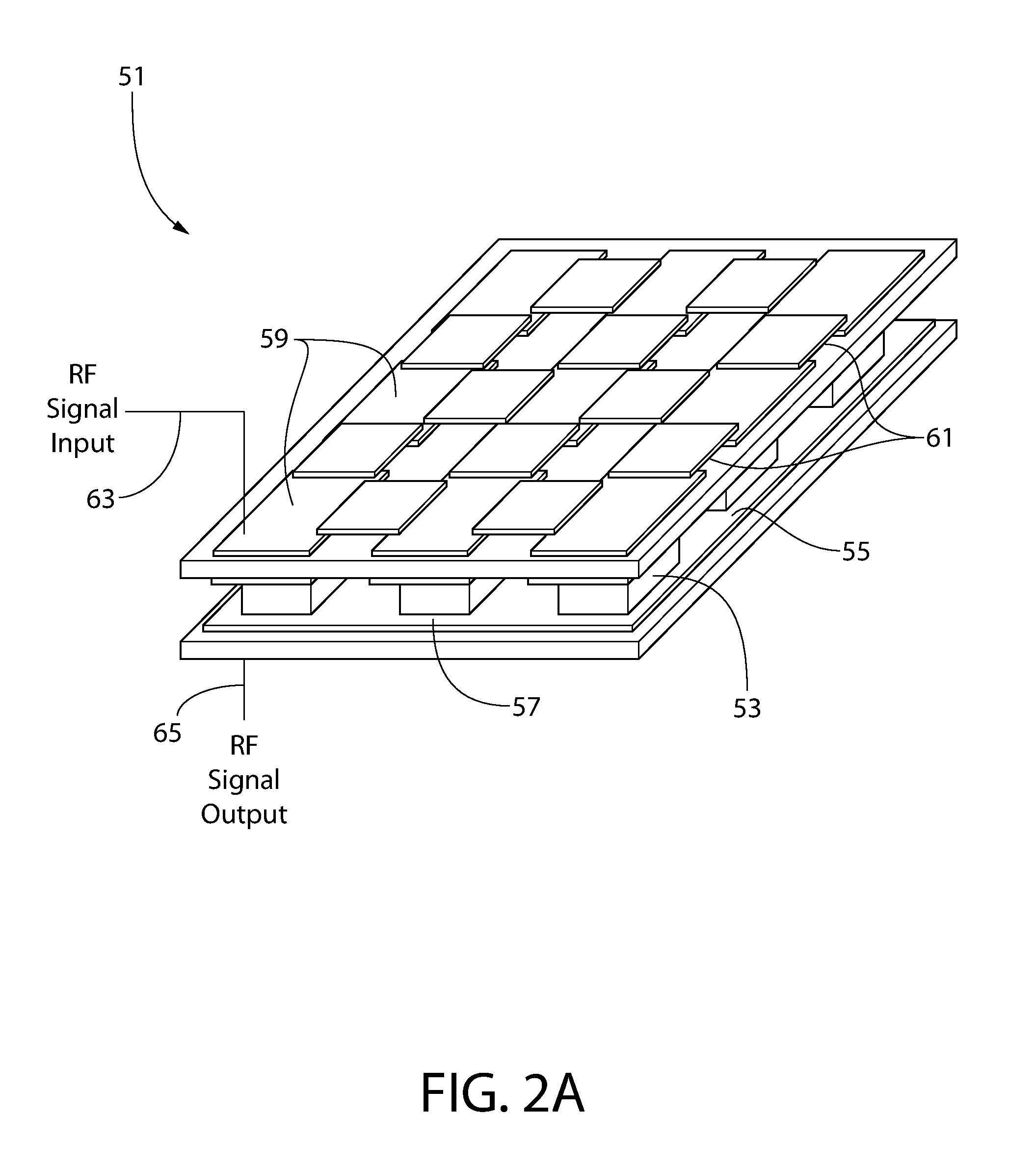
The series and shunt variable capacitors 31, 33 may each be an electronically variable capacitor 51 such as is depicted in FIG. 2A. The electronically variable capacitor 51 includes a plurality of discrete capacitors 53 which form an array, and each discrete capacitor 53 has an electrode on opposite sides thereof, such as is typical of discrete capacitors that are available on the market.
Each discrete capacitor 53 has its individual bottom electrode 55 electrically connected to a common bottom electrode 57. The individual top electrode 59 of each discrete capacitor 53 is electrically connected to the individual top electrode 59 of adjacent discrete capacitors 53 through an electronic switch 61 that may be activated to electrically connect the adjacent top electrodes 59. Thus, the individual top electrodes 59 of each discrete capacitor 53 may be electrically connected to the top electrodes 59 of one or more adjacent discrete capacitors 53. The electronic switch 61 is selected and/or designed to be capable of switching the voltage and current of the RF signal. For example, the electronic switch 61 may be a PiN/NiP diode, or a circuit based on a PiN/NiP diode. Alternatively, the electronic switch 61 may be any other type of appropriate switch, such as a micro electro mechanical (MEM) switch, a solid-state relay, a field effect transistor, and the like. One embodiment of the electronic switch 61, in combination with a driver circuit, is discussed in greater detail below.
In the configuration of the electronically variable capacitor 51 shown, each individual top electrode 59 may be electrically connected to between two to four adjacent top electrodes 59, with each connection being independently regulated by a separate electronic switch 61. The RF signal input 63 is electrically connected to one of the individual top electrodes 59, and the RF signal output 65 is electrically connected to the common bottom electrode 57. Thus, the electronic circuit through which the RF signal passes may include one, some, or all of the discrete capacitors 53 by a process of independently activating one or more of the electronic switches 61 coupled to adjacent ones of the individual top electrodes 59.
In other embodiments, the electronically variable capacitor 51 may be configured to have any layout for the individual top electrodes 59, to thereby increase or decrease the number of possible electrical connections between adjacent top electrodes 59. In still other embodiments, the electronically variable capacitor 51 may have an integrated dielectric disposed between the bottom electrode 57 and a plurality of top electrodes 59.
The electronic switch 61 that is used to connect pairs of adjacent top electrodes 59 may be a PiN/NiP diode-based switch, although other types of electronic switches may be used, such as a Micro Electro Mechanical (MEM) switch, a solid-state relay, a field effect transistor, and the like. Each electronic switch 61 is switched by appropriate driver circuitry. For example, each of the series and 651 shunt driver circuits 39, 43 of FIG. 1 may include several discrete driving circuits, with each discrete driving circuit configured to switch one of the electronic switches 61 between an on state and an off state. By controlling the on and off states of each discrete capacitor 53 within the electronically variable capacitor 51, the capacitance of the electronically variable capacitor 51 may be controlled and varied. Each unique configuration of the on and off states of the plurality of discrete capacitors 53 is referred to herein as an "array configuration" of the variable capacitor 51, and each array configuration is associated with a capacitance of the electronically variable capacitor 51. In certain embodiments, each array configuration results in a unique capacitance for the electronically variable capacitor 51, so that there is a direct correlation between each array configuration and the capacitance value of the electronically variable capacitor 51.
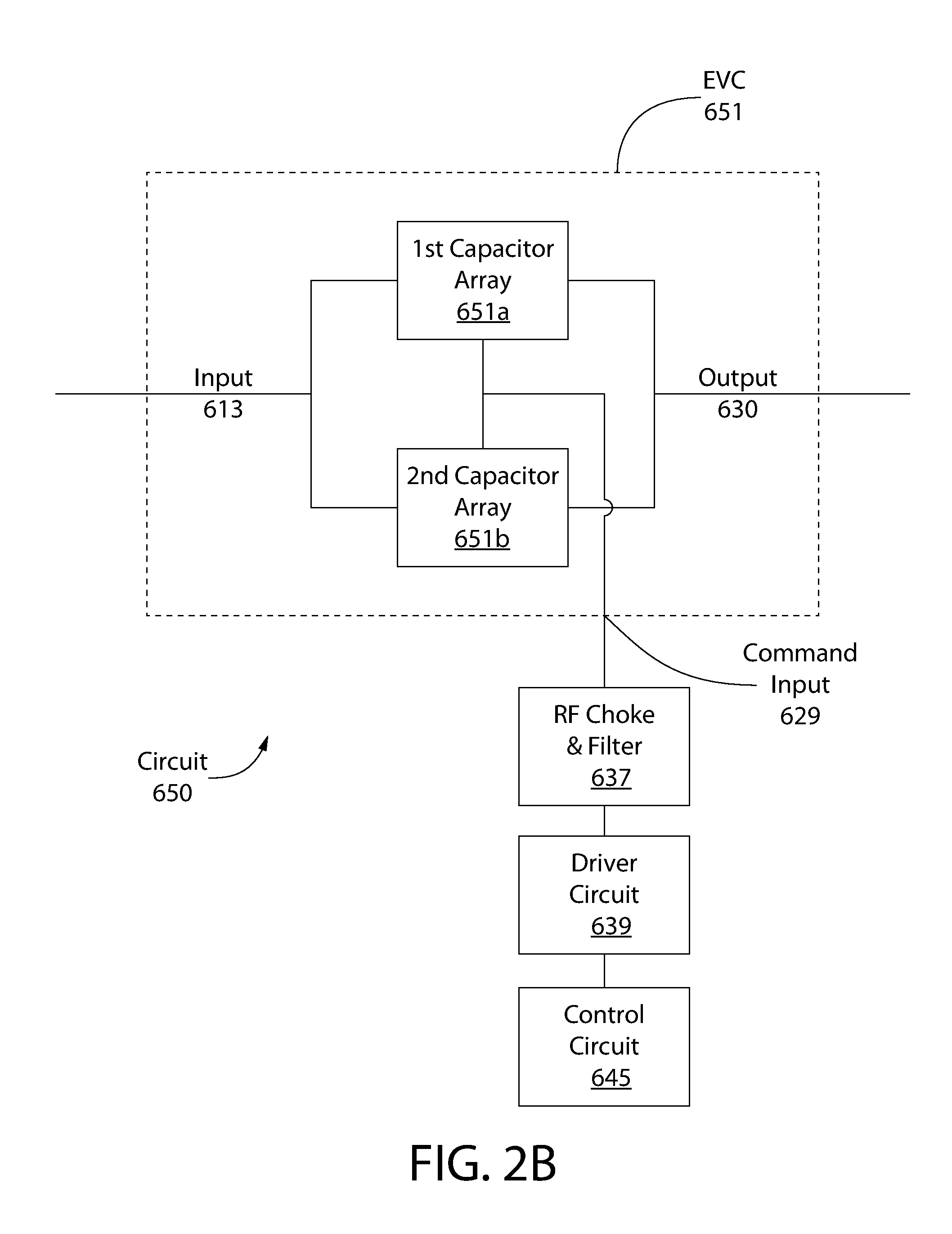
FIG. 2B shows an electronic circuit 650 for providing a variable capacitance according to one embodiment. The circuit 650 utilizes an EVC 651 that includes two capacitor arrays 651a, 651b. The first capacitor array 651a has a first plurality of discrete capacitors, each having a first capacitance value. The second capacitor array 651b has a second plurality of discrete capacitors, each having a second capacitance value. The first capacitance value is different from the second capacitance value such that the EVC 651 can provide coarse and fine control of the capacitance produced by the EVC 651. The first capacitor array and the second capacitor array are coupled in parallel between a signal input 613 and a signal output 630. The capacitor arrays 651a, 651b and their discrete capacitors may be arranged in manner similar to that shown in FIG. 2A, or in an alternative manner.
The first and second capacitance values can be any values sufficient to provide the desired overall capacitance values for the EVC 651. In one embodiment, the second capacitance value is less than or equal to one-half (1/2) of the first capacitance value. In another embodiment, the second capacitance value is less than or equal to one-third (1/3) of the first capacitance value. In yet another embodiment, the second capacitance value is less than or equal to one-fourth (1/4) of the first capacitance value.
The electronic circuit 650 further includes a control circuit 645. The control circuit 645 is operably coupled to the first capacitor array 651a and to the second capacitor array 651b by a command input 629, the command input 629 being operably coupled to the first capacitor array 651aand to the second capacitor array 651b. In the exemplified embodiment, the command input 629 has a direct electrical connection to the capacitor arrays 651a, 651b, though in other embodiments this connection can be indirect. The coupling of the control circuit 645 to the capacitor arrays 651a, 651b will be discussed in further detail below.
The control circuit 645 is configured to alter the variable capacitance of the EVC 651 by controlling on and off states of (a) each discrete capacitor of the first plurality of discrete capacitors and (b) each discrete capacitor of the second plurality of discrete capacitors. The control circuit 645 can have features similar to those described with respect to control circuit 45 of FIG. 1. For example, the control circuit 645 can receive inputs from the capacitor arrays 651a, 651b, make calculations to determine changes to capacitor arrays 651a, 651b, and delivers commands to the capacitor arrays 651a, 651b for altering the capacitance of the EVC 651.
Similar to EVC 51 discussed with respect to FIG. 2A, the EVC 651 of FIGS. 2B and 2C can include a plurality of electronic switches. Each electronic switch can be configured to activate and deactivate one or more discrete capacitors.
As with the control circuit 45 of FIG. 1, the control circuit 645 can also be connected to a driver circuit 639 and an RF choke and filter circuit 637. The control circuit 645, driver circuit 639, and RF choke and filter circuit 637 can have capabilities similar to those discussed with regard to FIG. 1. In the exemplified embodiment, the driver circuit 639 is operatively coupled between the control circuit 645 and the first and second capacitor arrays 651a, 651b. The driver circuit 639 is configured to alter the variable capacitance based upon a control signal received from the control circuit 645. The RF filter 637 is operatively coupled between the driver circuit 639 and the first and second capacitor arrays 651a, 651b. In response to the control signal sent by the control unit 645, the driver circuit 639 and RF filter 637 are configured to send a command signal to the command input 629. The command signal is configured to alter the variable capacitance by instructing at least one of the electronic switches to activate or deactivate (a) at least one the discrete capacitors of the first plurality of discrete capacitors or (b) at least one of the discrete capacitors of the second plurality of discrete capacitors.
In the exemplified embodiment, the driver circuit 639 is configured to switch a high voltage source on or off in less than 15 .mu.sec, the high voltage source controlling the electronic switches of each of the first and second capacitor arrays for purposes of altering the variable capacitance. The EVC 651, however, can be switched by any of the means or speeds discussed in the present application.
The control circuit 645 can be configured to calculate coarse and fine capacitance values to be provided by the respective capacitor arrays 651a, 651b. In the exemplified embodiment, the control circuit 645 is configured to calculate a coarse capacitance value to be provided by controlling the on and off states of the first capacitor array 651a. Further, the control circuit is configured to calculate a fine capacitance value to be provided by controlling the on and off states of the second capacitor array 651b. In other embodiments, the capacitor arrays 651a, 651b can provide alternative levels of capacitance.
In other embodiments, the EVC can utilize additional capacitor arrays. FIG. 2C shows an embodiment of an EVC 651' in which a third capacitor array 651c' is utilized to provide an additional degree of control over the variable capacitance. Like the EVC 651 of FIG. 2B, the EVC 651' of FIG. 2C includes an input 613', an output 630', and a command input 629'. Similar to the first and second capacitor arrays 651a', 651b', the third capacitor array 651c' can have a third plurality of discrete capacitors. Each discrete capacitor of the third plurality of discrete capacitors can have a third capacitance value, this value being different from both the first capacitance value and the second capacitance value. The first capacitor array 651a', second capacitor array 651b', and third capacitor array 651c' can be coupled in parallel between the signal input 613' and the signal output 630'. A control circuit can be operably coupled to the third capacitor array 651c', and be further configured to alter the variable capacitance by controlling on and off states of each discrete capacitor of the third plurality of discrete capacitors. Additional capacitor arrays enable an EVC to utilize several different capacitance values in controlling the overall EVC capacitance. In other embodiments, the third plurality of discrete capacitors can be replaced with a single discrete capacitor, or an alternative device for varying the overall capacitance of the EVC 651'.
The first, second, and third capacitance values of EVC 651' can be any values sufficient to provide the desired overall capacitance values for EVC 651'. In one embodiment, the second capacitance value is less than or equal to one-half (1/2) of the first capacitance value, and the third capacitance value is less than or equal to one-half (1/2) of the second capacitance value. In another embodiment, the second capacitance value is less than or equal to one-third (1/3) of the first capacitance value, and the third capacitance value is less than or equal to one-third (1/3) of the second capacitance value.
The EVCs 651, 651' of FIGS. 2B and 2C, respectively, can be used in most systems requiring a varying capacitance. For example, the EVCs 651, 651' can be used as a series EVC and/or a shunt EVC in a matching network, such as the RF matching network 11 discussed above with respect to FIG. 1. It is often desired that the differences between the capacitance values allow for both a sufficiently fine resolution of the overall capacitance of the circuit and a wide range of capacitance values to enable a better impedance match at the input of a RF matching network, and EVCs 651, 651' allow this.
The EVCs 651, 651' can also be used in a system or method for fabricating a semiconductor, a method for controlling a variable capacitance, and/or a method of controlling an RF impedance matching network. Such methods can include altering at least one of the series variable capacitance and the shunt variable capacitance to the determined series capacitance value and the shunt capacitance value, respectively. This altering can be accomplishing by controlling, for each of the series EVC and the shunt EVC, on and off states of each discrete capacitor of each plurality of discrete capacitors. In other embodiments, the EVC 651, 651' and circuit 650 can be used in other methods and systems to provide a variable capacitance.
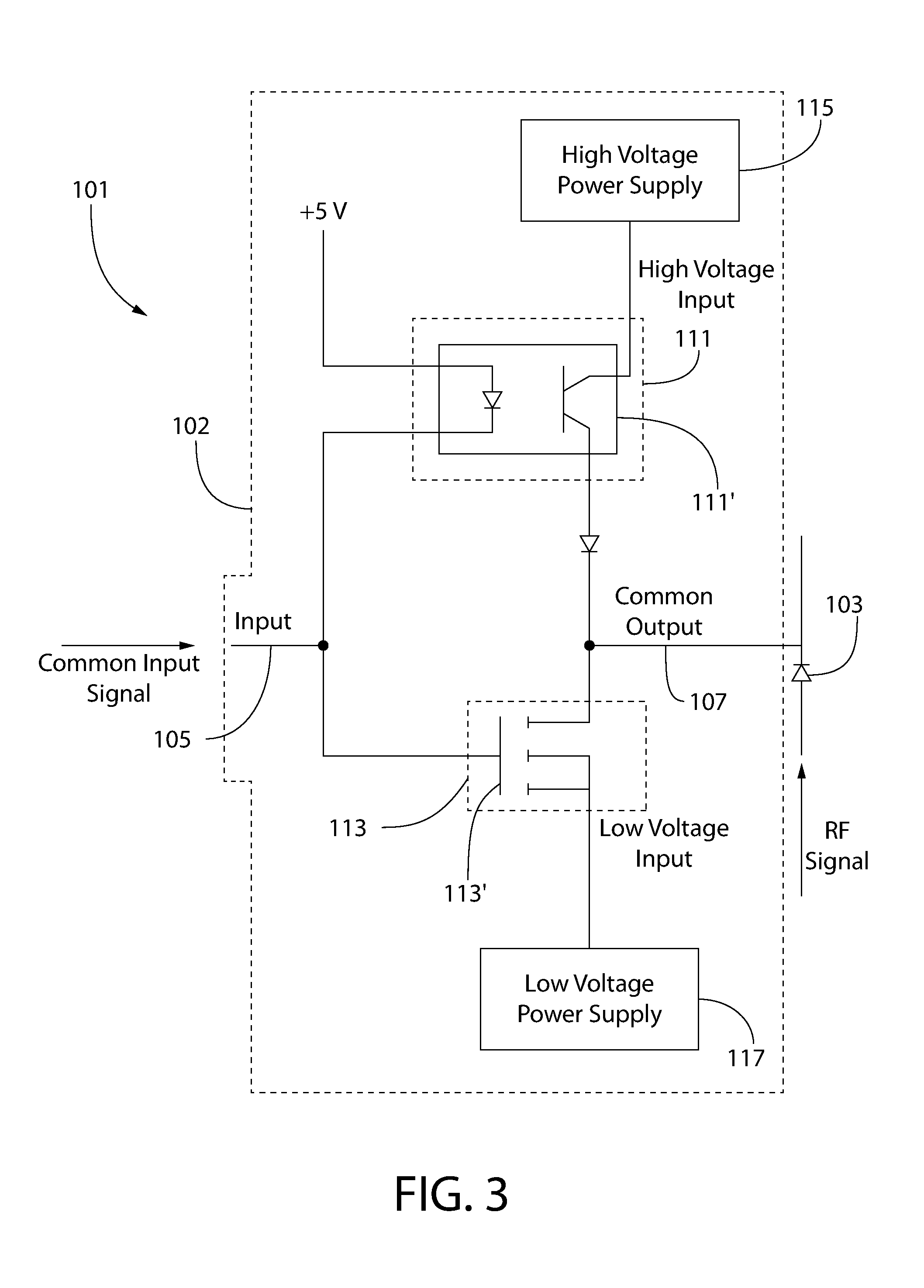
FIG. 3 shows an embodiment of a high voltage switching circuit 101, which is shown including a driver circuit 102 and a PiN/NiP diode 103 as an electronic switch. Although this switching circuit is shown with the driver circuit 102 integrated with the PiN/NiP diode 103, one of skill in the art will understand that in practice, the PiN/NiP diode 103, or any other type of electronic switch, may be integrated with the discrete capacitors in an EVC that is part of an RF impedance matching network, with the RF choke and filter circuit connected between the output of the driver circuit 102 and the PiN/NiP diode 103.
The switching circuit 101 may be used for switching one of the discrete capacitors in an EVC between an `ON` state and an `OFF` state. One of skill in the art will recognize that the use of the PiN/NiP diode 103 in this embodiment is exemplary, and that the switching circuit 101 may include other types of circuitry that does not include the PiN/NiP diode 103, yet still provides some of the same fast switching advantages of the PiN/NiP diode 103 for switching one of the discrete capacitors in an EVC. One of skill in the art will also recognize that certain components of the driver circuit 102 may be replaced with other components that perform the same essential function while also greater allowing variability in other circuit parameters (e.g., voltage range, current range, and the like).
This driver circuit 102 has an input 105 which receives a common input signal for controlling the voltage on the common output 107 that is connected to and drives the PiN/NiP diode 103. The voltage on the common output 107 switches the PiN/NiP diode 103 between the `ON` state and the `OFF` state, thus also switching `ON` and `OFF` the discrete capacitor to which the PiN/NiP diode 103 is connected. The state of the discrete capacitor, in this exemplary embodiment, follows the state of the state of the PiN/NiP diode 103, such that when the PiN/NiP diode 103 is `ON`, the discrete capacitor is also `ON`, and likewise, when the PiN/NiP diode 103 is `OFF`, the discrete capacitor is also `OFF`. Thus, statements herein about the state of the PiN/NiP diode 103 inherently describe the concomitant state of the connected discrete capacitor of the EVC.
The input 105 is connected to both a first power switch 111 and into a second power switch 113. As depicted, the first power switch 111 is an optocoupler phototransistor 111', and the second power switch 113 is a MOSFET 113'. A high voltage power supply 115 is connected to the first power switch 111, providing a high voltage input which is to be switchably connected to the common output 107. A low voltage power supply 117 is connected to the second power switch 113, providing a low voltage input which is also to be switchably connected to the common output 107. In the configuration of the driver circuit 102 shown, the low voltage power supply 117 may supply a low voltage input which is about -5 V. Such a low voltage, with a negative polarity, is sufficient to provide a forward bias for switching the PiN/NiP diode 103. For other configurations of the driver circuit 102, a higher or lower voltage input may be used, and the low voltage input may have a positive polarity, depending upon the configuration and the type of electronic switch being controlled.
The common input signal asynchronously controls the `on` and `off` states of the first power switch 111 and the second power switch 113, such that when the first power switch 111 is in the `on` state, the second power switch 113 is in the `off` state, and similarly, when the first power switch is in the `off` state, the second power switch 113 is in the `on` state. In this manner, the common input signal controls the first power switch 111 and the second power switch 113 to asynchronously connect the high voltage input and the low voltage input to the common output for purposes of switching the PiN/NiP diode 103 between the `ON` state and the `OFF` state.
The input 105 may be configured to receive any type of appropriate control signal for the types of switches selected for the first power switch 111 and the second power switch 113, which may be, for example, a +5 V control signal. Of course, to maintain simplicity of the overall driver circuit 102 and avoid incurring additional manufacturing costs, the first and second power switches 111, 113 are preferably selected so that they may directly receive the common input signal without requiring additional circuitry to filter or otherwise transform the common input signal.
The switching circuit 101 has design features which make it particularly useful for switching between a high voltage input and a low voltage input on the common output quickly and without the need to float the drive circuit, with respect to the high voltage input, or require use of special gate charging circuits due to isolation of the input signal from the high voltage input. Another advantage of the switching circuit 101 is that it provides the ability to switch the common output between voltage modes quickly, within the time frame of about 15 .mu.sec or less. The simplicity of the switching circuit 101 should considerably reduce manufacturing costs, especially when compared to other circuits performing similar functionality, and it should also significantly reduce space requirements for the circuit, and again, especially as compared to other circuits performing similar functionality. These advantages make the switching circuit 101 particularly advantageous with the incorporated PiN/NiP diode 103.
One of the ways in which these advances are realized is the first power switch 111 being a monolithic circuit element, such as the optocoupler phototransistor 111'. A monolithic element reduces both cost and space requirements. When an optocoupler phototransistor 111' is used as the monolithic element, it can perform the necessary high voltage switching quickly, and it serves to isolate the high voltage input from the common input signal. Other, as yet unrealized advantages may also be present through the use of an optocoupler phototransistor 111'.
An optocoupler phototransistor 111' serves well as the first power switch 111 for use in conjunction with the PiN/NiP diode 103 because of the low current requirements for the PiN/NiP diode 103 when in the `OFF` state. During the `OFF` state, the PiN/NiP diode 103 is reverse biased, and thus non-conducting, and as such the `OFF` state current requirement falls within the current handling capability of most optocoupler phototransistors. In addition, in implementations when one or both of the voltage requirements or the current requirements exceed the specifications for a single optocoupler phototransistor, additional optocoupler phototransistors may be added into the circuit in series or in parallel to increase the voltage and/or current handling capabilities of the switching circuit.
To further highlight the advantages of the switching circuit 101, its operation is detailed when the first power switch 111 is an optocoupler phototransistor 111' and the second power switch 113 is an appropriate MOSFET 113'. In this example, the common input signal may be a 5 V control signal which is alternated between a first voltage level and a second voltage level that serve to switch both the optocoupler phototransistor 111' and the MOSFET 113' between `on` and `off` states. The manner of implementing a 5 V control signal is well known to those of skill in the art.
When the PiN/NiP diode 103 is to be turned to the `OFF` state, the optocoupler phototransistor 111' is turned to the `on` state by applying the first voltage level from the common input signal across the photodiode inputs of the optocoupler phototransistor 111'. Turning the optocoupler phototransistor 111' to the `on` state connects high voltage input to the common output 107, thereby reverse biasing the PiN/NiP diode 103. At the same time, during this `OFF` state of the PiN/NiP diode 103, application of the first voltage level from the common input signal to the MOSFET 113' places the MOSFET 113' in the `off` state, thereby disconnecting low voltage input from the common output 107.
When the PiN/NiP diode 103 is to be turned to the `ON` state, the optocoupler phototransistor 111' is turned to the `off` state by applying the second voltage level from the common input signal across the photodiode inputs of the optocoupler phototransistor 111'. Turning the optocoupler phototransistor 111' to the `off` state disconnects high voltage input from the common output 107. At the same time, application of the second voltage level from the common input signal to the MOSFET 113' places the MOSFET 113' in the `on` state, thereby connecting the low voltage input to the common output 107. With the MOSFET 113' in the `on` state, and the optocoupler phototransistor 111' to the `off` state, only the low voltage input is connected to the common output 107, so that the PiN/NiP diode 103 is forward biased and placed in the `ON` state.
As indicated above, the optocoupler phototransistor 111' provides the advantage that the common input signal is electrically isolated, through the internal optical switch (not shown) of the optocoupler phototransistor 111', from the switched high voltage, thus alleviating the need to float the drive circuit (such as when a MOSFET is used to switch the high voltage). Use of the optocoupler phototransistor 111' provides the additional advantage that the driver circuit 102 can quickly switch the common output 107 between the high voltage input and the low voltage input, with the switching occurring within the time frame of about 15 .mu.sec or less. This fast switching time helps reduce switching loss, thereby reducing stress on the PiN/NiP diode itself, and introduces improvements in the semiconductor fabrication process by reducing the amount of time it takes for the RF impedance matching network to create an impedance match between the RF source and the plasma chamber.
The use of optocoupler phototransistors in the driver circuit 102 also provides advantages for switching a high voltage input in the range of 500 V-1000 V. Higher or lower voltages may also be switched with this driver circuit 102. The high voltage input may therefore differ from the low voltage input by at least two or three orders of magnitude, or more. Advantageously, when the switching circuit 101 incorporates the PiN/NiP diode 103, the high voltage input and the low voltage input may have opposite polarities.
The ability of the driver circuit 102 to provide quick switching capabilities is exemplified by the graphs 151, 161 of FIGS. 4 and 5. The voltage curve 153 of FIG. 4 shows the voltage on the common output 107 of the driver circuit 102 in order to switch the connected PiN/NiP diode 103 to the `OFF` state. As is shown by the voltage curve 153, the driver circuit 102 is capable of switching to connect the high voltage input, which in this example is approximately 1,000 V, to the common output 107 within about 11 .mu.sec. The voltage curve 163 of FIG. 5 shows the voltage on the common output 107 of the driver circuit 102 in order to switch the connected PiN/NiP diode 103 to the `ON` state. As is shown by the voltage curve 163, the driver circuit 102 is capable of switching to connect the low voltage input, which in this example is approximately -12 V, to the common output 107 within about 9 .mu.sec. Thus, an RF impedance matching network which includes EVCs and switching circuits, as described above, shows significant improvements as compared to an RF impedance matching network which includes VVCs.
A switching circuit 201 which includes a driver circuit 202 having multiple optocoupler phototransistors 203 to increase the high voltage capabilities is shown in FIG. 6A. Like the driver circuit 102 of FIG. 3, this driver circuit 202 includes an input 205 which receives a common input signal for controlling the voltage on the common output 207. The switching circuit 201 includes a PiN/NiP diode 209 connected to the common output 207, and the voltage on the common output 207 may be used to switch the PiN/NiP diode 209 between `ON` state and `OFF` states. The input 205 is connected to both a first power switch 211, which includes the optocoupler phototransistors 203, and to a second power switch 213, which includes another optocoupler phototransistor 215 and a MOSFET 217.
A high voltage power supply 219 is connected to the first power switch 211, providing a high voltage input which is to be switchably connected to the common output 207. A low voltage power supply 221 is connected to the second power switch 213, providing a low voltage input which is also to be switchably connected to the common output 207.
The optocoupler phototransistors 203 of the first power switch 211 are connected in series to each other in order to enable the first power switch 211 to switch higher voltages onto the common output 207 in the same manner as discussed above with a single optocoupler phototransistor. With appropriate selection of the optocoupler phototransistors 203, the first power switch 211, as shown, is capable of switching about 1000 V or more from the high voltage power supply 219 to the common output 207. Additional optocoupler phototransistors may be added in series for the first power switch 211 to increase the high voltage switching capabilities. One of skill in the art will recognize that one or more optocoupler phototransistors may be connected in parallel to each other to increase the current load capabilities of the first power switch 211. One optocoupler phototransistor may be used to switch low voltages through the design rating of the optocoupler phototransistor, with more optocoupler phototransistors being added to switch higher voltages.
The optocoupler phototransistor 215 of the second power switch 213 receives the common input signal, like the optocoupler phototransistors 203 of the first power switch 211. This optocoupler phototransistor 215 is connected to the MOSFET 217 and places the MOSFET 217 in the `off` state by connecting the source to the gate when the common input signal places the first power switch 211 in the `on` state. In this configuration, when the MOSFET 217 is in the `on` state, the second power switch 213 is also in the `on` state, connecting the low power input to the common output 207 Likewise, when the MOSFET 217 is in the `off` state, the second power switch 213 is also in the `off` state, so that the low power input is disconnected from the common output 207. When the first power switch is in the `off` state, optocoupler phototransistor 215 disconnects the gate from the source, so that the MOSFET 217 placed in the `on` state by the gate being connected to the voltage V2, which is an appropriate voltage for controlling the gate of the MOSFET 217.
FIG. 6B shows a switching circuit 201-1 according to yet another embodiment of the invention. In this embodiment, the switching circuit 201-1 can utilize a cascode structure 218-1 to increase high voltage capabilities and increase switching speed while providing a simple control scheme.
In the exemplified embodiment, the switching circuit 201-1 includes a driver circuit 202-1 (sometimes referred to as a control circuit) and a PiN/NiP diode 209-1. As in other embodiments, the driver circuit 202-1 includes an input 205-1 that receives a common input signal for controlling the voltage on the common output 207-1. The PiN/NiP diode 209-1 is connected to the common output 207-1, and the voltage on the common output 207-1 may be used to switch the PiN/NiP diode 209-1 between `ON` and `OFF` states. The common input 205-1 is connected to both a first power switch 211-1 and a second power switch 213-1.
As with switching circuits 101 and 201, switching circuit 201-1 may be used for switching one of the discrete capacitors in an EVC between an `ON` state and an `OFF` state. One of skill in the art will recognize that the use of the PiN/NiP diode 209-1 in this embodiment is exemplary, and that the switching circuit 201-1 may include other types of circuitry that does not include the PiN/NiP diode 209-1, yet still provides some of the same advantages of the PiN/NiP diode 209-1 for switching one of the discrete capacitors in an EVC. One of skill in the art will also recognize that certain components of the driver circuit 202-1 may be replaced with other components that perform the same essential function while also greater allowing variability in other circuit parameters (e.g., voltage range, current range, and the like). One of skill in the art will also recognize that certain commonly known components have been omitted from discussion for clarity.
The PiN/NiP diode 209-1 is configured to receive an RF signal. In the exemplified embodiment, the RF signal is a high voltage RF signal (e.g., 1000 V peak amplitude, 3000 V peak amplitude, or 4000 V peak amplitude). Accordingly, a high voltage power supply (e.g., 1200 VDC for a 1000V peak amplitude RF signal) is required to reverse bias the PiN/NiP diode 209-1 and thereby turn the switching circuit 201-1 `OFF`. The high voltage of the high voltage power supply 219-1 can be two orders of magnitude or more greater than the low voltage of the low voltage power supply 221-1.
The high voltage power supply 219-1 is connected to the first power switch 211-1, providing a high voltage input which is to be switchably connected to the common output 207-1. A low voltage power supply 221-1 is connected to the second power switch 213-1, providing a low voltage input which is also to be switchably connected to the common output 207-1. In the configuration of the driver circuit 202-1 shown, the low voltage power supply 221-1 may supply a low voltage input which is about -5 V. Such a low voltage, with a negative polarity, is sufficient to provide a forward bias for switching the PiN/NiP diode 209-1. For other configurations of the driver circuit 202-1, a higher or lower voltage input may be used, and the low voltage input may have a positive polarity, depending upon the configuration and the type of electronic switch being controlled.
The common input signal asynchronously controls the `on` and `off` states of the first power switch 211-1 and the second power switch 213-1, such that when the first power switch 211-1 is in the `on` state, the second power switch 213-1 is in the `off` state, and similarly, when the first power switch 211-1 is in the `off` state, the second power switch 213-1 is in the `on` state. In this manner, the common input signal controls the first power switch 211-1 and the second power switch 213-1 to asynchronously connect the high voltage input and the low voltage input to the common output for purposes of switching the PiN/NiP diode 209-1 between the `ON` state and the `OFF` state.
The common input 205-1 may be configured to receive any type of appropriate control signal for the types of switches selected for the first power switch 211-1 and the second power switch 213-1, which may be, for example, a +5 V control signal.
The switching circuit 201-1 has design features which make it particularly useful for switching between a high voltage input and a low voltage input on the common output quickly and without the need to float the drive circuit, with respect to the high voltage input, or require use of special gate charging circuits due to isolation of the input signal from the high voltage input. Another advantage of the switching circuit 201-1 is that it can provide the ability to switch the common output between voltage modes quickly, within the time frame of about 5 .mu.sec or less. The simplicity of the switching circuit 201-1 should considerably reduce manufacturing costs, especially when compared to other circuits performing similar functionality, and it should also significantly reduce space requirements for the circuit, and again, especially as compared to other circuits performing similar functionality. These advantages make the switching circuit 201-1 particularly advantageous with the incorporated PiN/NiP diode 209-1.
Similar to first power switches 111 and 211, first power switch 211-1 can utilize at least one optocoupler phototransistor 203-1. (The terms optocoupler and optocoupler phototransistor are used interchangeably herein.) In the exemplified embodiment, three optocoupler phototransistors 203-1 are utilized. The high voltage power supply 219-1 is connected to the collector port of the topmost optocoupler phototransistor 203-1. Advantages of the use of optocoupler phototransistors in the first power switch are discussed above. The optocoupler phototransistors 203-1 of the first power switch 211-1 are connected in series to each other to enable the first power switch 211-1 to switch higher voltages onto the common output 207 in a manner similar to that discussed above. With appropriate selection of the optocoupler phototransistors 203-1, the first power switch 211-1 is capable of switching 1000 V or more from the high voltage power supply 219-1 to the common output 207-1. In other embodiments, additional optocoupler phototransistors may be added in series for the first power switch 211-1 to increase the high voltage switching capabilities. In yet other embodiments, fewer optocoupler phototransistors may be used, including use of a single optocoupler phototransistor.
The second power switch 213-1 can include a cascode structure 218-1 designed to increase the blocking voltage capability of the switching circuit 201-1. The cascode structure 218-1 includes multiple JFETs J1, J2, J3 in series. These JFETs are connected in series with a low-voltage MOSFET M2. As a non-limiting example, the JFETs can be 1700 VDC JFETs, while and the MOSFET can be a 30V MOSFET. Specifically, the MOSFET M2 is connected in series between the JFETs J1, J2, J3 the and low voltage power supply. Between each of the JFET gates is a diode D5, D6. In other embodiments, a single JFET (rather than multiple JFETs) can be utilized for the cascode structure. A voltage source V2 is connected to the gate of MOSFET M2. The voltage source V2 is also connected to optocoupler phototransistor 215-1 (sometimes referred to as input optocoupler 215-1). When the optocoupler phototransistor 215-1 is turned on, the optocoupler phototransistor 215-1 can essentially short the gate of MOSFET M2 to the source of MOSFET M2, turning MOSFET M2 `off`. It is noted that the JFETs, MOSFETs, and optocoupler phototransistors can be replaced with other appropriate transistors or switches. Accordingly, a JFET such as one of JFETs J1, J2, J3 can be referred to as a first transistor, and a MOSFET such as MOSFET M2 can be referred to as a second transistor.
When the PiN/NiP diode 209-1 is in the `ON` state, the first power switch 211-1 is in the `off` state and the second power switch 213-1 is in the `on` state. In the exemplified embodiment, the PiN/NiP diode 209-1 is put in the `ON` state by applying a first common input signal of +0 V at the common input 205-1. When the +0 V first common input signal is applied, input MOSFET M3 (which can be another type of transistor, such as a BJT, and is sometimes referred to as the input transistor) is turned `off`. Consequently, no current flows through the photodiode inputs of the optocoupler phototransistors 203-1, 215-1. Thus, the optocoupler transistors 203-1, 215-1 are turned `off`, common output 207-1 does not receive high voltage from the high voltage power supply 219-1, and the diode 209-1 is not reverse biased.
At the same time, since optocoupler 215-1 is `off`, the gate of MOSFET M2 can receive a voltage from voltage V2. R1 and R2 form a voltage divider for voltage V2, so that the gate of MOSFET M2 receives a divided voltage from V2. In the exemplified embodiment, voltage V2 is +5 V. The receipt of divided voltage V2 at the gate of MOSFET M2 causes MOSFET M2 to switch `on`, which turns `on` the first JFET J1 since the gate of first JFET J1 is then connected to its source. Next, the second JFET J2 can start conducting and turn `on`, since the voltage on the gate of JFET J5 is -V.sub.F (the forward voltage drop of diode D6). The same process can be repeated for turning `on` the remaining JFETs (third JFET J3), until the voltage of the low voltage power supply 221-1 appears at the common output 207-1, thereby providing the necessary biasing voltage to forward bias PiN/NiP diode 209-1.
With the MOSFET M2 in the `on` state, and the optocoupler phototransistors 203-1, 215-1 in the `off` state, only the low voltage input is connected to the common output 209-1, so that the PiN/NiP diode 209-1 is forward biased and placed in the `ON` state. When the optocouplers 203-1 of the first power switch are switched off, a voltage drop from the high voltage (of high voltage power supply 219-1) to the low voltage (of the low voltage power supply 221-1) occurs across the plurality of optocouplers.
By contrast, when the PiN/NiP diode 209-1 is in the `OFF` state, the first power switch 211-1 is in the `on` state and the second power switch 213-1 is in the `off` state. In the exemplified embodiment, the PiN/NiP diode 209-1 is put in the `ON` state by applying a second common input signal of +5 V at the common input 205-1. When the +5 V first common input signal is applied, input MOSFET M3 is turned `on`. Consequently, current flows through the photodiode inputs of the optocoupler phototransistors 203-1, 215-1. Thus, the optocoupler transistors 203-1, 215-1 are turned `on`, and common output 207-1 receives high voltage from the high voltage power supply 219-1 to reverse bias diode 209-1.
At the same time, the gate of MOSFET M2 does not receive voltage V2, because optocoupler 215-1 is `on`, and therefore diverts voltage from the gate of MOSFET M2. Since the gate of MOSFET M2 does not receive voltage V2, MOSFET M2 switches `off`, which causes JFETS J1, J2, J3 to turn off, thereby preventing the low voltage of the low voltage power supply 221-1 to appear at the common output 207-1.
In this state, where the first power switch 211-1 is switched `on` and the second power switch 213-1 is switched `off`, the high voltage power source can cause a large voltage across the MOSFET M2 and the JFETs J1, J2, J3. One benefit of this structure is that the MOSFET M2 can be a low-voltage MOSFET (e.g., 30 V), while the JFETs J1, J2, J3 can be higher-voltage JFETS (e.g., 1700 V) for handling the high voltage from the high voltage power source. For different applications, the MOSFET M2 can remain the same (in number and type), while the number or type of JFETs can be adjusted to handle the voltage requirements. Building a higher voltage switch can be achieved by simply adding one or more JFETs in series with the existing JFETs. There is no need to alter the switch configuration or how the switch needs to be driven. In this manner, the cascode structure increases the blocking voltage capability of the switching circuit.
With MOSFET M2 in the `off` state, and the optocoupler phototransistors 203-1, 215-1 in the `on` state, only the high voltage input is connected to the common output 209-1, so that the PiN/NiP diode 209-1 is reverse biased and placed in the `ON` state.
The non-linear capacitance range of a single EVC switched by a switching circuit is shown in the graph 301 of FIG. 7. The single EVC used to generate the capacitance curve 303 has 24 discrete capacitors in the manner described above, with the top electrodes of the discrete capacitors being selectively connected to arrive at the capacitance curve 303 shown. As can be seen, the single EVC may provide a capacitance ranging from only one active discrete capacitor (i.e., none of the top electrodes of any of the discrete capacitors are connected, so that the RF signal only flows through a single discrete capacitor) to all 24 discrete capacitors being active (i.e., all the top electrodes of all the discrete capacitors are connected). Any number of the 24 discrete capacitors may be connected, so that the capacitance of the single EVC may range from a low capacitance, with one active discrete capacitor as part of the array configuration, to a high capacitance, with all 24 discrete capacitors active as part of the array configuration. The low capacitance and the high capacitance are a matter of design choice for the EVC. In the capacitance curve shown, the low capacitance is about 25 pF, while the high capacitance is over 1,600 pF. The number of discrete capacitance values that is achievable between the low capacitance and the high capacitance is also a matter of design choice for the EVC, as more or fewer discrete capacitors may be included as part of the EVC. The only significant constraints on an EVC are the mechanical limitations posed by specific implementations (e.g., size or weight restrictions on the EVC). Mechanical limitations aside, an EVC does not appear to have any issues for achieving high value capacitance (e.g., 200,000 pF or higher).
The stable delivered power of an RF impedance matching network incorporating EVCs is shown in the graph 331 of FIG. 8, which does not show or take into account switching capabilities of an EVC controlled by a switching circuit. There are three curves shown in this graph 331: the output power 333 of the RF signal output from the RF source, which is about 500 V; the delivered power 335 to the plasma chamber; and the reflected power 337 back to the RF source. The output power 333 is a little over 500 V, while the reflected power 337 is in the range of about 10 V, so that the delivered power 335 to the plasma chamber is about 500 V. Not only is the delivered power 335 about 98% of the output power 333, but the delivered power 335, as can be seen, is substantially stable, without significant fluctuations. Both the percentage of delivered power 335 and the stability of the delivered power 335 represent significant improvements over an RF impedance matching network that is based on VVCs.
When the switching capabilities of an EVC controlled by a switching circuit, in the manner described above, are incorporated into an RF impedance matching network, high speed switching is enabled for the RF impedance matching network. FIG. 9 is a graph 401 having voltage along the two y-axes and time along the x-axis to show the speed at which an RF impedance matching network using EVCs performs impedance matching (also referred to as the "match tune process"). A representation of an RF power profile 403 is shown, taken at the RF input of an RF impedance matching network, and the y-axis for the RF power profile has 50 mV divisions. A representation of the voltage of the common input signal 405 for driver circuits is also shown in the lower portion of the graph 401, the common input signal 405 originating from the control circuit of the RF impedance matching network, and the y-axis for the common input signal 405 has 5 V divisions. The x-axis has 50 .mu.sec divisions, with the 56 .mu.sec point marked in approximately the middle of the graph and the t=0 point as marked.
Initially, a significant amount of reflected power 407 is shown in the left portion of the RF power profile 403 (i.e., before the 56 .mu.sec mark). This reflected power represents inefficiencies in the RF power being transferred between the RF source and the plasma chamber as a result of an impedance mismatch. At about t=-36 .mu.sec, the match tune process begins. The first approximately 50 .mu.sec of the match tune process is consumed by measurements and calculations performed by the control circuit in order to determine new values for the variable capacitances of one or both of the series and shunt EVCs.
FIG. 10 is a flow chart showing a process 500 for matching an impedance according to one embodiment. Similar to the matching networks discussed above, the matching network 11 of the exemplified process includes the following (shown in FIG. 1): an RF input 13 configured to operably couple to an RF source 15, the RF source 15 having a fixed RF source impedance (e.g., 50 Ohms); an RF output 17 configured to operably couple to a plasma chamber 19, the plasma chamber 19 having a variable plasma impedance; a series electronically variable capacitor ("series EVC") 31 having a series array configuration, the series EVC 31 electrically coupled in series between the RF input 13 and the RF output 17; a shunt electronically variable capacitor ("shunt EVC") 33 having a shunt array configuration, the shunt EVC 33 electrically coupled in parallel between a ground 40 and one of the RF input 13 and the RF output 17; an RF input sensor 21 operably coupled to the RF input 13, the RF input sensor 21 configured to detect an RF input parameter at the RF input 13; an RF output sensor 49 operably coupled to the RF output 17, the RF output sensor 49 configured to detect an RF output parameter; and a control circuit 45 operatively coupled to the series EVC 31 and to the shunt EVC 33 to control the series array configuration and the shunt array configuration. The steps of the exemplified process 500 can be carried out as part of the manufacture of a semiconductor, where a substrate 27 is placed in a plasma chamber 19 configured to deposit a material layer onto the substrate 27 or etch a material layer from the substrate 27, and plasma is energized within the plasma chamber 19 by coupling RF power from the RF source 15 into the plasma chamber 19 to perform a deposition or etching.
In the exemplified process 500 of FIG. 10, the control circuit 45 is configured and/or programmed to carry out each of the steps. As one of two initial steps, RF parameters are measured at the RF input 13 by the RF input sensor 21, and the input impedance at the RF input 13 is calculated (step 501) using the measured RF parameters. For this exemplified process 500, the forward voltage and the forward current are measured at the RF input 13. In certain other embodiments, the RF parameters may be measured at the RF output 17 by the RF output sensor 49, although in such embodiments, different calculations may be required than those described below. In still other embodiments, RF parameters may be measured at both the RF input 13 and the RF output 17.
The impedance matching circuit, coupled between the RF source 15 and the plasma chamber 19, may be characterized by one of several types of parameter matrices known to those of skill in the art. An S-parameter matrix and a Z-parameter matrix are two examples of such parameter matrices. Other examples include, but are not limited to, a Y-parameter matrix, a G-parameter matrix, an H-parameter matrix, a T-parameter matrix, and an ABCD-parameter matrix. Those of skill in the art will recognize also that these various parameter matrices may be mathematically converted from one to the other for an electrical circuit such as a matching network. The second initial step of the exemplified process 500 is to look up (step 502) the parameter matrix for the existing configuration of the impedance matching circuit in a parameter look-up table. The existing configuration of the impedance matching circuit is defined by existing operational parameters of the impedance matching circuit, particularly the existing array configurations for both of the series EVC 31 and the shunt EVC 33. In order to achieve an impedance match, the existing configuration of the impedance matching circuit is altered to a new configuration of the impedance matching circuit as part of the exemplified process 500.
The parameter look-up table includes a plurality of parameter matrices, with each parameter matrix being associated with a particular configuration of the series EVC 31 and the shunt EVC 33. The parameter look-up table may include one or more of the aforementioned types of parameter matrices. In the exemplified process 500, the parameter look-up table includes at least a plurality of S-parameter matrices. In certain embodiments, the parameter look-up table may include at least a plurality of Z-parameter matrices. In embodiments in which the parameter look-up table includes multiple types of parameter matrices, the different types of parameter matrices are associated within the parameter look-up table in such a way so as to eliminate the need for mathematical conversions between the different types of parameter matrices. For example, the T-parameter matrix may be included as part of the parameter look-up table, with each T-parameter matrix associated with the associated S-parameter matrix that would result from conversion between the two matrices.
The input impedance calculation (step 501) and the parameter matrix look up (step 502) may be performed in any order. With the input impedance calculated (step 501) and the parameter matrix for the existing configuration of the impedance matching circuit identified within the parameter look-up table (step 502) done, the plasma or load impedance may then be calculated (step 503) using the calculated input impedance and the parameter matrix for the existing configuration. Next, from the calculated plasma impedance, the match configurations for the series EVC 31 and the shunt EVC 33 that would achieve an impedance match, or at least a substantial impedance match, between the RF source 15 and the plasma chamber 19 are looked up (step 504) in an array configuration look-up table. These match configurations from the array configuration look-up table are the array configurations which will result in new capacitance values for the series EVC 31 and shunt EVC 33, with an impedance match being achieved with the new array configurations and associated new capacitance values. The array configuration look-up table is a table of array configurations for the series EVC 31 and the shunt EVC 33, and it includes each possible array configuration of the series EVC 31 and the shunt EVC 33 when used in combination. As an alternative to using an array configuration look-up table, the actual capacitance values for the EVCs 31, 33 may be calculated during the process--however, such real-time calculations of the capacitance values are inherently slower than looking up the match configurations in the array configuration look-up table. After the match configurations for the series EVC 31 and the shunt EVC 33 are identified in the array configuration look-up table, then one or both of the series array configuration and the shunt array configuration are altered (step 505) to the respective identified match configurations for the series EVC 31 and the shunt EVC 33.
The altering (step 505) of the series array configuration and the shunt array configuration may include the control circuit 45 sending a control signal to the series driver circuit 39 and the shunt driver circuit 43 to control the series array configuration and the shunt array configuration, respectively, where the series driver circuit 39 is operatively coupled to the series EVC 31, and the shunt driver circuit 43 is operatively coupled to the shunt EVC 43. When the EVCs 31, 33 are switched to the match configurations, the input impedance may match the fixed RF source impedance (e.g., 50 Ohms), thus resulting in an impedance match. If, due to fluctuations in the plasma impedance, a sufficient impedance match does not result, the process of 500 may be repeated one or more times to achieve an impedance match, or at least a substantial impedance match.
The look-up tables used in the process described above are compiled in advance of the RF matching network being used in conjunction with the plasma chamber 19. In creating the look-up tables, the RF matching network 11 is tested to determine at least one parameter matrix of each type and the load impedance associated with each array configuration of the series EVC 31 and the shunt EVC 33 prior to use with a plasma chamber. The parameter matrices resulting from the testing are compiled into the parameter look-up table so that at least one parameter matrix of each type is associated with a respective array configuration of the EVCs 31, 33. Similarly, the load impedances are compiled into the array configuration look-up table so that each parameter matrix is associated with a respective array configuration of the EVCs 31, 33. The pre-compiled look-up tables may take into consideration the fixed RF source impedance (e.g., 50 Ohms), the power output of the RF source, and the operational frequency of the RF source, among other factors that are relevant to the operation of the RF matching network. Each look-up table may therefore have tens of thousands of entries, or more, to account for all the possible configurations of the EVCs 31, 33. The number of possible configurations is primarily determined by how many discrete capacitors make up each of the EVCs 31, 33. In compiling the look-up tables, consideration may be given to possible safety limitations, such as maximum allowed voltages and currents at critical locations inside the matching network, and this may serve to exclude entries in one or more of the look-up tables for certain configurations of the EVCs 31, 33.
As is known in the art, the S-parameter matrix is composed of components called scatter parameters, or S-parameters for short. An S-parameter matrix for the impedance matching circuit has four S-parameters, namely S.sub.11, S.sub.12, S.sub.21, and S.sub.22, each of which represents a ratio of voltages at the RF input 13 and the RF output 17. All four of the S-parameters for the impedance matching circuit are determined and/or calculated in advance, so that the full S-parameter matrix is known. The parameters of the other types of parameter matrices may be similarly determined and/or calculated in advance and incorporated into the parameter matrix. For example, a Z-parameter matrix for the impedance matching circuit has four Z-parameters, namely Z.sub.11, Z.sub.12, Z.sub.21, and Z.sub.22.
By compiling the parameter look-up table in this manner, the entire time cost of certain calculations occurs during the testing phase for the RF matching network, and not during actual use of the RF matching network 11 with a plasma chamber 19. Moreover, because locating a value in a look-up table can take less time than calculating that same value in real time, using the look-up table can aid in reducing the overall time needed to achieve an impedance match. In a plasma deposition or etching process which includes potentially hundreds or thousands of impedance matching adjustments throughout the process, this time savings can help add directly to cost savings for the overall fabrication process.
From the beginning of the match tune process, which starts with the control circuit determining the variable impedance of the plasma chamber and determining the series and shunt match configurations, to the end of the match tune process, when the RF power reflected back toward the RF source decreases, the entire match tune process of the RF impedance matching network using EVCs has an elapsed time of approximately 110 .mu.sec, or on the order of about 150 .mu.sec or less. This short elapsed time period for a single iteration of the match tune process represents a significant increase over a VVC matching network. Moreover, because of this short elapsed time period for a single iteration of the match tune process, the RF impedance matching network using EVCs may iteratively perform the match tune process, repeating the two determining steps and the generating another control signal for further alterations to the array configurations of one or both of the electronically variable capacitors. By iteratively repeating the match tune process, it is anticipated that a better impedance match may be created within about 2-4 iterations of the match tune process. Moreover, depending upon the time it takes for each repetition of the match tune process, it is anticipated that 3-4 iterations may be performed in 500 .mu.sec or less. Given the 1-2 sec match time for a single iteration of a match tune process for RF impedance matching networks using VVCs, this ability to perform multiple iterations in a fraction of the time represents a significant advantage for RF impedance matching networks using EVCs.
Those of skill in the art will recognize that several factors may contribute to the sub-millisecond elapsed time of the impedance matching process for an RF impedance matching network using EVCs. Such factors may include the power of the RF signal, the configuration and design of the EVCs, the type of matching network being used, and the type and configuration of the driver circuit being used. Other factors not listed may also contribute to the overall elapsed time of the impedance matching process. Thus, it is expected that the entire match tune process for an RF impedance matching network having EVCs should take no more than about 500 .mu.sec to complete from the beginning of the process (i.e., measuring by the control circuit and calculating adjustments needed to create the impedance match) to the end of the process (the point in time when the efficiency of RF power coupled into the plasma chamber is increased due to an impedance match and a reduction of the reflected power). Even at a match tune process on the order of 500 .mu.sec, this process time still represents a significant improvement over RF impedance matching networks using VVCs.
Table 1 presents data showing a comparison between operational parameters of one example of an EVC versus one example of a VVC. As can be seen, EVCs present several advantages, in addition to enabling fast switching for an RF impedance matching network:
TABLE-US-00001 TABLE 1 Typical 1000 pF Parameter EVC Vacuum Capacitors Capacitance 20 pF~1400 pF 15 pF~1000 pF Reliability High Low Response Time ~500 .mu.sec 1 s~2 s ESR ~13 mW ~20 mW Voltage 7 kV 5 kV Current Handling Capability 216 A rms 80 A rms Volume 4.5 in.sup.3 75 in.sup.3
As is seen, in addition to the fast switching capabilities made possible by the EVC, EVCs also introduce a reliability advantage, a current handling advantage, and a size advantage. Additional advantages of the RF impedance matching network using EVCs and/or the switching circuit itself for the EVCs include: The disclosed RF impedance matching network does not include any moving parts, so the likelihood of a mechanical failure reduced to that of other entirely electrical circuits which may be used as part of the semiconductor fabrication process. For example, the typical EVC may be formed from a rugged ceramic substrate with copper metallization to form the discrete capacitors. The elimination of moving parts also increases the resistance to breakdown due to thermal fluctuations during use. The EVC has a compact size as compared to a VVC, so that the reduced weight and volume may save valuable space within a fabrication facility. The design of the EVC introduces an increased ability to customize the RF matching network for specific design needs of a particular application. EVCs may be configured with custom capacitance ranges, one example of which is a non-linear capacitance range. Such custom capacitance ranges can provide better impedance matching for a wider range of processes. As another example, a custom capacitance range may provide more resolution in certain areas of impedance matching. A custom capacitance range may also enable generation of higher ignition voltages for easier plasma strikes. The short match tune process (.about.500 .mu.sec or less) allows the RF impedance matching network to better keep up with plasma changes within the fabrication process, thereby increasing plasma stability and resulting in more controlled power to the fabrication process. The use of EVCs, which are digitally controlled, non-mechanical devices, in an RF impedance matching network provides greater opportunity to fine tune control algorithms through programming. EVCs exhibit superior low frequency (kHz) performance as compared to VVCs. Enclosure Cooling System
In systems such as the matching networks and semiconductor manufacturing systems discussed above, heat can be generated that compromises system operation. The embodiments discussed below can be utilized to help cool such systems, as well as other types of systems.
In one embodiment, the embodiments can enhance the cooling capacity of a water-cooling heat sink by adding a heat exchanger to the heat sink and mounting a fan directly over or adjacent to the heat exchanger. By this design, when electrical components heat the air within an enclosure, the fan can blow the heated air onto the heat exchanger of the heat sink. The heat sink can transfer the heat to cool water running through a tube (e.g., a copper pipe) in the heat sink. The heated water can then be removed from the heat sink at a water output, thereby removing heat from the enclosure. Since the heat that is built up is removed by the heat sink by way of the cool water, the generator enclosure can be totally sealed to the outside atmosphere. This in turn eliminates the outgassing concern from damaged components and assemblies and prevents contamination of the fab.
FIG. 11 show a system 710 according to one embodiment of the invention. In the exemplified embodiment, the system 710 includes a matching network, such as the matching networks discussed above. In other embodiments, the system can be any system generating heat, including an RF generator, or a combination RF generator and matching network. In the exemplified embodiment, the system 710 includes electrical components 717, 718 for a matching network, and the matching networks forms part of a semiconductor manufacturing system, such as the systems discussed above.
The exemplified system 710 includes an enclosure 712 and a cooling system 720. FIG. 11 shows a side view of the system 710 where a side panel of the enclosure 712 is removed. Within the enclosure 712 are shelf electrical components 717 located on a component shelf 714, as well as other electrical components 718. The exemplified enclosure 712 (when the front side panel is in place) is sealed so as to prevent air and exhaust from escaping the enclosure. While no enclosure is completely sealed to prevent the escape of all air and exhaust, the enclosure is designed to reasonably prevent most air and exhaust from escaping. This can prevent outgassing and contamination of the surrounding environment, which is particularly helpful in a semiconductor fab.
The cooling system 720 includes a heat sink 730 and a fan 750 enclosed by the enclosure 712 for causing air flow A. In the exemplified embodiment, the heat sink 730 is within the enclosure 712, though in other embodiments a portion of the heat sink may be outside the enclosure 712. The fan 750 can direct hot air A from the first electrical components 718 to the heat exchanger 740 of the heat sink 730. The fan 750 can be mounted on or adjacent to the heat sink. As used herein, the term "fan" refers to any device for pushing air within the system to be cooled.
Cool water enters the heat sink 730 at the water input 764. The cool water travels through a tube 762 in the heat sink 730. Heat is transferred from the heat exchanger 740 to the water flowing through the heat exchanger 740, and the heated water is removed from the heat sink 730 at the water output 766, thereby removing heat from the enclosure 712. It is noted that, while the exemplified embodiment utilizes water traveling through the tube, other liquids can be utilized instead of water.
FIGS. 12-14 show the heat sink 730 apart from the enclosure 712 and the other components of the cooling system 720. FIG. 12 is a perspective bottom view of the heat sink 730. The heat sink 730 includes a main housing portion 732 and a heat exchanger portion 740.
The heat exchanger 740 can be affixed directly to the main housing 732 of the heat sink 730. In another embodiment, the heat exchanger can be created by cutting fins directly into the heat sink 730. Affixed fins can be, for example, die cast or molded. The heat exchanger 740 can be made of a material with a high rate of thermal conductivity (e.g., aluminum or copper). The geometry of the heat exchanger 740 increases the surface area of contact between the tube 738 (and the water it carries) and the heated air. This configuration pulls heat away from the air in the enclosure 712 at a high rate, cooling the air and, consequently, the electrical components 718. The geometry of the heat exchanger 740 can any geometry that effectively increases the surface area of the tube 738. As used herein, the term "heat exchanger" can refer to any device configured to transfer heat from one medium to another.
The main housing 732 can have a main housing surface 733 that can receive electrical components or rest against a surface that receives electrical components. The water flow W of the cool water in the tube 762 is shown. The tube 762 can extend into and out of the heat exchanger 740, the tube 762 configured to transport water through the heat exchanger 740. The tube 762 can also extend into and out of the main housing 732. In other embodiments, the main housing 732 can be omitted, and the tube 762 can extend through the heat exchanger 740.
FIG. 13 shows a perspective top view of the heat sink 730. In the exemplified embodiment, the main housing top surface 734 can be attached to the component shelf surface 716 (FIG. 11) such that the two surfaces 734, 716 are in contact with each other. The surfaces 734, 716 can comprise thermally conductive material. In another embodiment, the main housing surface (top 734 or bottom 733) can be configured to received electrical components directly on the main housing surface 734, 733.
FIG. 14 shows bottom view of the heat sink 730. The exemplified main housing 732 has a first edge 737 and a second edge 738 opposite the first edge 737. The heat exchanger 740 has a first edge 742 and a second edge 744 opposite the first edge 742. The main housing second edge 738 is adjacent the heat exchanger first edge 742. The tube 762 enters the main housing 732 at the main housing first edge 737. The tube 762 enters the heat exchanger 740 at the heat exchanger first edge 742. The tube 762 exits the heat exchanger 740 at the heat exchanger first edge 742. Further, the tube 762 exits the main housing 732 at the main housing first edge 737. The main housing 32 and the heat exchanger 40 are located side-by-side and contact each other along edges 28 and 42, respectively. In the exemplified heat sink, the tube 762 extends along a first side 35 of the main housing 32 and a second side 36 of the main housing 32 opposite the first side 35.
In other embodiments, other configurations can be utilized. For example, the main housing could be eliminated, or the tube could enter that heat exchanger before entering the main housing. Further, rather than entering along a first side and then exiting along a second, opposite side, the tube could proceed in any manner, such as zig-zagging back-and-forth between the two sides.
In addition to the foregoing, means can be provided inside the system to detect the fault and generate a fault signal that causes the removal of power from the system to prevent further damage. For example, a fault signal could cause the removal of power from the inputs of an RF generator and an RF matching network to prevent further damage. In one embodiment, the fault signal can be received by a control circuit, such as control circuit 45 (FIG. 1), which in turn causes the removal of power from the inputs. The unit can go to a safe condition and send an alarm to a host computer in a fab. This can be accomplished with a variety of sensors that monitor various conditions. For example, the sensors can include an ambient air temperature sensor and a heat sink temperature. Other features that can be monitored include a blocked fan, over dissipation, and/or a power supply failure. By monitoring such features and triggering a fault, the system can not only prevent the outgassing of gases from failed components, but can also restrict the amount of outgassing by terminating the power that feeds into the failure, thus limiting the damage, preventing more serious failure, and preventing the failure of other associated circuitry outside the enclosed system. In addition to or in place of the fault signal that is communicated to the semiconductor fabrication system, the RF generator or the RF matching network may open the system interlock, directly resulting in the shutdown of any power generation source connected to the inputs of the RF generator or the RF matching network.
Since the enclosure is completely enclosed, any humidity left in the enclosure may condense as the chamber is heated and cooled. Therefore, it may be necessary to either purge the enclosure with a small flow of clean dry air or Nitrogen (N.sub.2) with a return port for exhausting this flow so as to maintain the integrity of the enclosure to the outside atmosphere. Alternatively, ports might be provided to purge the enclosure with Nitrogen to remove the humidity and then close the ports after sealing the enclosure.
FIG. 15 is a flow chart for a method 770 of cooling an enclosure according to one embodiment. The exemplified method 770 cools an enclosure that encloses electrical components and is sealed to prevent air and exhaust from escaping the enclosure, though the invention is not so limited. The method 770 comprises positioning a heat sink at least partially within the enclosure (operation 771). Similar to above, the heat sink comprises a heat exchanger and a tube extending into and out of the heat exchanger, the tube configured to transport water through the heat exchanger. The method 770 further comprises, by a fan enclosed by the enclosure, pushing air heated by electrical components onto the heat exchanger (operation 772). The method 770 further comprises receiving, at the heat exchanger, heat from the pushed air (operation 773), and transferring, by the heat exchanger, the received heat to water being transported by the tube through the heat exchanger (operation 774).
In another embodiment, a method of manufacturing a semiconductor is utilized. The method includes operably coupling a matching network between an RF source and a plasma chamber, for example, as in FIG. 1 described above. The plasma chamber is configured to deposit a material layer onto the substrate or etch a material layer from the substrate, and electrical components of the matching network are enclosed by an enclosure (such as enclosure 712 discussed above) that is configured to prevent air and exhaust from escaping the enclosure. The method also includes positioning a heat sink (such as heat sink 730 discussed above) at least partially within the enclosure; placing a substrate in the plasma chamber; energizing plasma within the plasma chamber by coupling RF power from the RF source into the plasma chamber to perform a deposition or etching; by a fan enclosed by the enclosure, pushing air heated by electrical components onto the heat exchanger; receiving, at the heat exchanger, heat from the pushed air; and transferring, by the heat exchanger, the received heat to water being transported by the tube through the heat exchanger.
Some of the foregoing embodiments discuss use of cooling system for an RF system used in semiconductor manufacturing. It is noted, however, that the invention is not so limited, as the cooling systems and methods can be used with other systems that require cooling.
While the invention has been described with respect to specific examples including presently preferred modes of carrying out the invention, those skilled in the art will appreciate that there are numerous variations and permutations of the above described systems and techniques. It is to be understood that other embodiments may be utilized and structural and functional modifications may be made without departing from the scope of the present invention. Thus, the spirit and scope of the invention should be construed broadly as set forth in the appended claims.
* * * * *
D00000
D00001
D00002
D00003
D00004
D00005
D00006
D00007
D00008
D00009
D00010
D00011
D00012
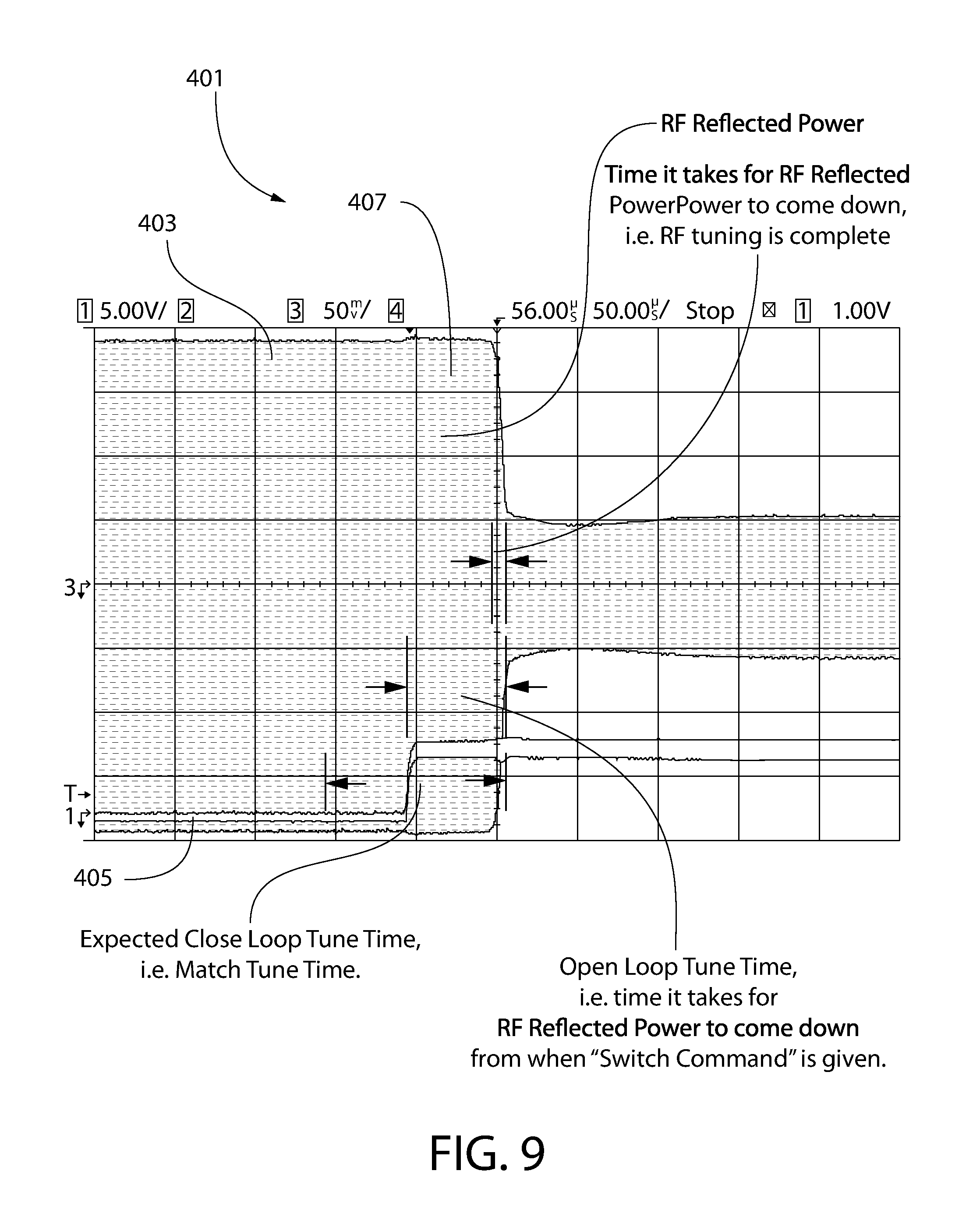
D00013
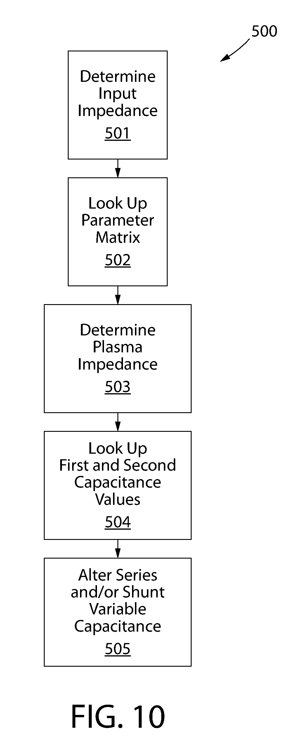
D00014

D00015
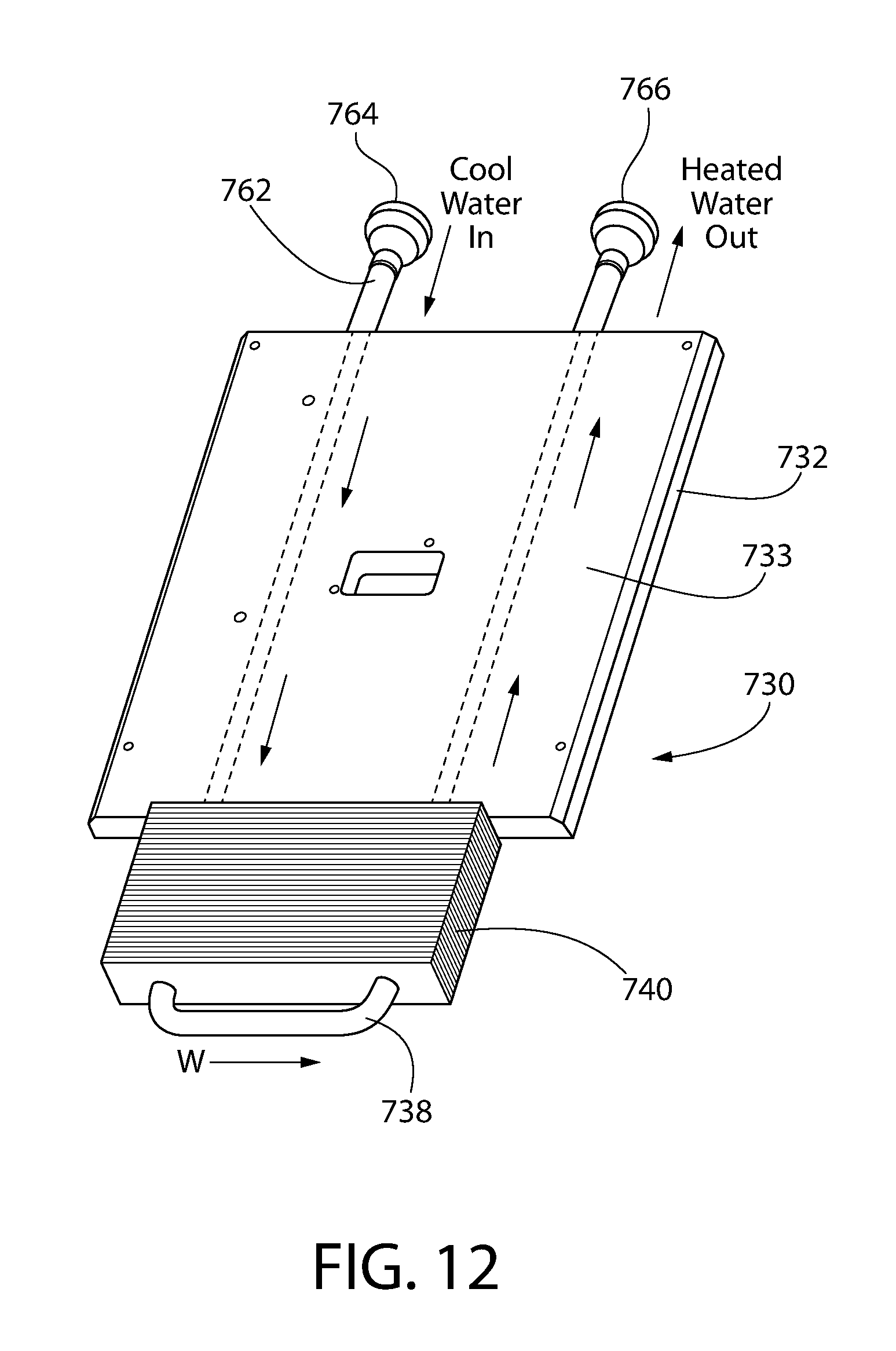
D00016
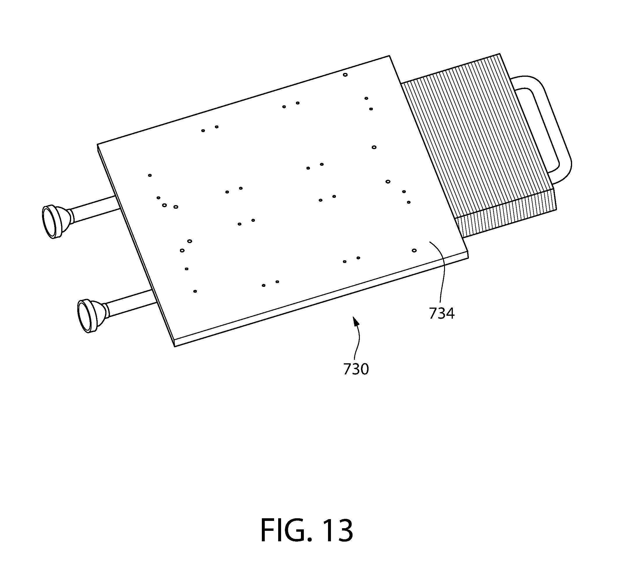
D00017

D00018

XML
uspto.report is an independent third-party trademark research tool that is not affiliated, endorsed, or sponsored by the United States Patent and Trademark Office (USPTO) or any other governmental organization. The information provided by uspto.report is based on publicly available data at the time of writing and is intended for informational purposes only.
While we strive to provide accurate and up-to-date information, we do not guarantee the accuracy, completeness, reliability, or suitability of the information displayed on this site. The use of this site is at your own risk. Any reliance you place on such information is therefore strictly at your own risk.
All official trademark data, including owner information, should be verified by visiting the official USPTO website at www.uspto.gov. This site is not intended to replace professional legal advice and should not be used as a substitute for consulting with a legal professional who is knowledgeable about trademark law.