Methods of fabricating magnetic tunnel junctions integrated with selectors
Kim , et al. O
U.S. patent number 10,438,996 [Application Number 15/865,247] was granted by the patent office on 2019-10-08 for methods of fabricating magnetic tunnel junctions integrated with selectors. This patent grant is currently assigned to Spin Memory, Inc.. The grantee listed for this patent is Spin Transfer Technologies, Inc.. Invention is credited to Dafna Beery, Kuk-Hwan Kim, Amitay Levi, Andy Walker.


View All Diagrams
| United States Patent | 10,438,996 |
| Kim , et al. | October 8, 2019 |
Methods of fabricating magnetic tunnel junctions integrated with selectors
Abstract
Methods of fabricating devices including arrays of integrated Magnetic Tunnel Junctions (MTJs) and corresponding selectors in an array of cells. The array of cells can include a plurality of source lines disposed in columns, set of selectors coupled to respective source lines, MJT structures coupled to respective selectors and a plurality of bit lines disposed in rows and coupled to respective sets of MTJ structures. The array of cells can also include buffers coupled between respective selectors and respective MTJ structures. In addition, multiple arrays can be fabricated on top of each other to implement vertical three-dimensional (3D) MTJ devices.
| Inventors: | Kim; Kuk-Hwan (Fremont, CA), Beery; Dafna (Fremont, CA), Walker; Andy (Fremont, CA), Levi; Amitay (Fremont, CA) | ||||||||||
|---|---|---|---|---|---|---|---|---|---|---|---|
| Applicant: |
|
||||||||||
| Assignee: | Spin Memory, Inc. (Fremont,
CA) |
||||||||||
| Family ID: | 67143764 | ||||||||||
| Appl. No.: | 15/865,247 | ||||||||||
| Filed: | January 8, 2018 |
Prior Publication Data
| Document Identifier | Publication Date | |
|---|---|---|
| US 20190214430 A1 | Jul 11, 2019 | |
| Current U.S. Class: | 1/1 |
| Current CPC Class: | H01L 43/12 (20130101); G11C 11/161 (20130101); H01L 21/76802 (20130101); H01L 21/76877 (20130101); H01L 27/224 (20130101); H01F 10/3272 (20130101); H01L 45/146 (20130101); H01L 21/7684 (20130101); H01F 41/32 (20130101); H01F 10/3286 (20130101); H01L 45/1233 (20130101); H01L 45/1608 (20130101); H01F 10/3254 (20130101); H01L 43/02 (20130101); G11C 2211/5615 (20130101); H01L 21/3212 (20130101); H01L 45/08 (20130101); H01F 10/329 (20130101); H01L 43/10 (20130101); G11C 11/1659 (20130101) |
| Current International Class: | H01L 27/22 (20060101); H01L 21/768 (20060101); H01L 43/12 (20060101); H01L 43/02 (20060101); G11C 11/16 (20060101); H01F 10/32 (20060101); H01L 45/00 (20060101); H01F 41/32 (20060101); H01L 43/10 (20060101); H01L 21/321 (20060101) |
References Cited [Referenced By]
U.S. Patent Documents
| 4597487 | July 1986 | Crosby et al. |
| 5541868 | July 1996 | Prinz |
| 5559952 | September 1996 | Fujimoto |
| 5629549 | May 1997 | Johnson |
| 5640343 | June 1997 | Gallagher et al. |
| 5654566 | August 1997 | Johnson |
| 5691936 | November 1997 | Sakakima et al. |
| 5695846 | December 1997 | Lange et al. |
| 5695864 | December 1997 | Slonczewski |
| 5732016 | March 1998 | Chen et al. |
| 5751647 | May 1998 | O'Toole |
| 5856897 | January 1999 | Mauri |
| 5896252 | April 1999 | Kanai |
| 5966323 | October 1999 | Chen et al. |
| 6016269 | January 2000 | Peterson et al. |
| 6055179 | April 2000 | Koganei et al. |
| 6064948 | May 2000 | West |
| 6075941 | June 2000 | Itoh |
| 6097579 | August 2000 | Gill |
| 6112295 | August 2000 | Bhamidipati et al. |
| 6124711 | September 2000 | Tanaka et al. |
| 6134138 | October 2000 | Lu et al. |
| 6140838 | October 2000 | Johnson |
| 6154139 | November 2000 | Kanai et al. |
| 6154349 | November 2000 | Kanai et al. |
| 6172902 | January 2001 | Wegrowe et al. |
| 6233172 | May 2001 | Chen et al. |
| 6233690 | May 2001 | Choi et al. |
| 6243288 | June 2001 | Ishikawa et al. |
| 6252798 | June 2001 | Satoh et al. |
| 6256223 | July 2001 | Sun |
| 6292389 | September 2001 | Chen et al. |
| 6347049 | February 2002 | Childress et al. |
| 6376260 | April 2002 | Chen et al. |
| 6385082 | May 2002 | Abraham et al. |
| 6436526 | August 2002 | Odagawa et al. |
| 6442681 | August 2002 | Ryan et al. |
| 6458603 | October 2002 | Kersch et al. |
| 6493197 | December 2002 | Ito et al. |
| 6522137 | February 2003 | Sun et al. |
| 6532164 | March 2003 | Redon et al. |
| 6538918 | March 2003 | Swanson et al. |
| 6545903 | April 2003 | Savtchenko et al. |
| 6545906 | April 2003 | Savtchenko et al. |
| 6563681 | May 2003 | Sasaki et al. |
| 6566246 | May 2003 | deFelipe et al. |
| 6603677 | August 2003 | Redon et al. |
| 6653153 | November 2003 | Doan et al. |
| 6654278 | November 2003 | Engel et al. |
| 6677165 | January 2004 | Lu et al. |
| 6710984 | March 2004 | Yuasa et al. |
| 6713195 | March 2004 | Wang et al. |
| 6714444 | March 2004 | Huai et al. |
| 6731537 | May 2004 | Kanamori |
| 6744086 | June 2004 | Daughton et al. |
| 6750491 | June 2004 | Sharma et al. |
| 6765824 | July 2004 | Kishi et al. |
| 6772036 | August 2004 | Eryurek et al. |
| 6773515 | August 2004 | Li et al. |
| 6777730 | August 2004 | Daughton et al. |
| 6785159 | August 2004 | Tuttle |
| 6812437 | November 2004 | Levy et al. |
| 6829161 | December 2004 | Huai et al. |
| 6835423 | December 2004 | Chen et al. |
| 6838740 | January 2005 | Huai et al. |
| 6839821 | January 2005 | Estakhri |
| 6842317 | January 2005 | Sugita et al. |
| 6847547 | January 2005 | Albert et al. |
| 6887719 | May 2005 | Lu et al. |
| 6888742 | May 2005 | Nguyen et al. |
| 6902807 | June 2005 | Argoitia et al. |
| 6906369 | June 2005 | Ross et al. |
| 6920063 | July 2005 | Huai et al. |
| 6933155 | August 2005 | Albert et al. |
| 6938142 | August 2005 | Pawlowski |
| 6958927 | October 2005 | Nguyen et al. |
| 6967863 | November 2005 | Huai |
| 6980469 | December 2005 | Kent et al. |
| 6985385 | January 2006 | Nguyen et al. |
| 6992359 | January 2006 | Nguyen et al. |
| 6995962 | February 2006 | Saito et al. |
| 7002839 | February 2006 | Kawabata et al. |
| 7005958 | February 2006 | Wan |
| 7006371 | February 2006 | Matsuoka |
| 7006375 | February 2006 | Covington |
| 7009877 | March 2006 | Huai et al. |
| 7041598 | May 2006 | Sharma |
| 7045368 | May 2006 | Hong et al. |
| 7057922 | June 2006 | Fukumoto |
| 7170778 | January 2007 | Kent et al. |
| 7187577 | March 2007 | Wang |
| 7190611 | March 2007 | Nguyen et al. |
| 7203129 | April 2007 | Lin et al. |
| 7227773 | June 2007 | Nguyen et al. |
| 7262941 | August 2007 | Li et al. |
| 7307876 | December 2007 | Kent et al. |
| 7324387 | January 2008 | Bergemont et al. |
| 7335960 | February 2008 | Han et al. |
| 7351594 | April 2008 | Bae et al. |
| 7352021 | April 2008 | Bae et al. |
| 7372722 | May 2008 | Jeong |
| 7376006 | May 2008 | Bednorz et al. |
| 7386765 | June 2008 | Ellis |
| 7436699 | October 2008 | Tanizaki |
| 7449345 | November 2008 | Horng et al. |
| 7453719 | November 2008 | Sakimura |
| 7476919 | January 2009 | Hong et al. |
| 7502249 | March 2009 | Ding |
| 7573737 | August 2009 | Kent et al. |
| 7598555 | October 2009 | Papworth-Parkin |
| 7619431 | November 2009 | DeWilde et al. |
| 7642612 | January 2010 | Izumi et al. |
| 7660161 | February 2010 | Van Tran |
| 7733699 | June 2010 | Roohparvar |
| 7773439 | August 2010 | Do et al. |
| 7776665 | August 2010 | Izumi et al. |
| 7852662 | December 2010 | Yang et al. |
| 7881095 | February 2011 | Lu et al. |
| 7911832 | March 2011 | Kent et al. |
| 7936595 | May 2011 | Han et al. |
| 7986544 | July 2011 | Kent et al. |
| 8080365 | December 2011 | Nozaki |
| 8088556 | January 2012 | Nozaki |
| 8094480 | January 2012 | Tonomura |
| 8144509 | March 2012 | Jung |
| 8148970 | April 2012 | Fuse |
| 8255742 | August 2012 | Ipek |
| 8278996 | October 2012 | Miki |
| 8279666 | October 2012 | Dieny et al. |
| 8334213 | December 2012 | Mao |
| 8349536 | January 2013 | Nozaki |
| 8363465 | January 2013 | Kent et al. |
| 8386836 | February 2013 | Burger |
| 8432727 | April 2013 | Ryu |
| 8441844 | May 2013 | El Baraji |
| 8456883 | June 2013 | Liu |
| 8456926 | June 2013 | Ong |
| 8492881 | July 2013 | Kuroiwa et al. |
| 8535952 | September 2013 | Ranjan et al. |
| 8539303 | September 2013 | Lu |
| 8549303 | October 2013 | Fifield et al. |
| 8574928 | November 2013 | Satoh et al. |
| 8582353 | November 2013 | Lee |
| 8593868 | November 2013 | Park |
| 8617408 | December 2013 | Balamane |
| 8625339 | January 2014 | Ong |
| 8634232 | January 2014 | Oh |
| 8716817 | May 2014 | Saida |
| 8737137 | May 2014 | Choy et al. |
| 8780617 | July 2014 | Kang |
| 8792269 | July 2014 | Abedifard |
| 8852760 | October 2014 | Wang et al. |
| 8902628 | December 2014 | Ha |
| 8966345 | February 2015 | Wilkerson |
| 9019754 | April 2015 | Bedeschi |
| 9026888 | May 2015 | Kwok |
| 9043674 | May 2015 | Wu |
| 9082888 | July 2015 | Kent et al. |
| 9104595 | August 2015 | Sah |
| 9140747 | September 2015 | Kim |
| 9165629 | October 2015 | Chih |
| 9166155 | October 2015 | Deshpande |
| 9229853 | January 2016 | Khan |
| 9245608 | January 2016 | Chen et al. |
| 9250990 | February 2016 | Motwani |
| 9263667 | February 2016 | Pinarbasi |
| 9298552 | March 2016 | Leem |
| 9299412 | March 2016 | Naeimi |
| 9317429 | April 2016 | Ramanujan |
| 9337412 | May 2016 | Pinarbasi et al. |
| 9362486 | June 2016 | Kim et al. |
| 9378817 | June 2016 | Kawai |
| 9396991 | July 2016 | Arvin et al. |
| 9401336 | July 2016 | Arvin et al. |
| 9406876 | August 2016 | Pinarbasi |
| 9418721 | August 2016 | Bose |
| 9449720 | September 2016 | Lung |
| 9450180 | September 2016 | Annunziata |
| 9455013 | September 2016 | Kim |
| 9472282 | October 2016 | Lee |
| 9472748 | October 2016 | Kuo et al. |
| 9484527 | November 2016 | Han et al. |
| 9488416 | November 2016 | Fujita et al. |
| 9508456 | November 2016 | Shim |
| 9548445 | January 2017 | Lee et al. |
| 9553102 | January 2017 | Wang |
| 9583167 | February 2017 | Chung |
| 9728712 | August 2017 | Kardasz et al. |
| 9741926 | August 2017 | Pinarbasi et al. |
| 9772555 | September 2017 | Park et al. |
| 9773974 | September 2017 | Pinarbasi et al. |
| 9853006 | December 2017 | Arvin et al. |
| 9853206 | December 2017 | Pinarbasi et al. |
| 9853292 | December 2017 | Loveridge et al. |
| 9865806 | January 2018 | Choi et al. |
| 9972775 | May 2018 | Shum |
| 10026609 | July 2018 | Sreenivasan et al. |
| 10043851 | August 2018 | Shen |
| 10115446 | October 2018 | Louie et al. |
| 10163479 | December 2018 | Yoha |
| 2002/0057593 | May 2002 | Hidaka |
| 2002/0090533 | July 2002 | Zhang et al. |
| 2002/0105823 | August 2002 | Redon et al. |
| 2002/0132140 | September 2002 | Igarashi et al. |
| 2003/0085186 | May 2003 | Fujioka |
| 2003/0117840 | June 2003 | Sharma et al. |
| 2003/0151944 | August 2003 | Saito |
| 2003/0197984 | October 2003 | Inomata et al. |
| 2003/0218903 | November 2003 | Luo |
| 2004/0012994 | January 2004 | Slaughter et al. |
| 2004/0026369 | February 2004 | Ying |
| 2004/0047179 | March 2004 | Chan |
| 2004/0061154 | April 2004 | Huai et al. |
| 2004/0094785 | May 2004 | Zhu et al. |
| 2004/0130936 | July 2004 | Nguyen et al. |
| 2004/0173315 | September 2004 | Leung |
| 2004/0197174 | October 2004 | Van Den Berg |
| 2004/0221030 | November 2004 | Huras |
| 2004/0257717 | December 2004 | Sharma et al. |
| 2005/0022746 | February 2005 | Lampe |
| 2005/0029551 | February 2005 | Atwood et al. |
| 2005/0041342 | February 2005 | Huai et al. |
| 2005/0051820 | March 2005 | Stojakovic et al. |
| 2005/0063222 | March 2005 | Huai et al. |
| 2005/0104101 | May 2005 | Sun et al. |
| 2005/0128842 | June 2005 | Wei |
| 2005/0136600 | June 2005 | Huai |
| 2005/0158881 | July 2005 | Sharma |
| 2005/0160205 | July 2005 | Kuo |
| 2005/0174702 | August 2005 | Gill |
| 2005/0180202 | August 2005 | Huai et al. |
| 2005/0184839 | August 2005 | Nguyen et al. |
| 2005/0201023 | September 2005 | Huai et al. |
| 2005/0237787 | October 2005 | Huai et al. |
| 2005/0251628 | November 2005 | Jarvis et al. |
| 2005/0280058 | December 2005 | Pakala et al. |
| 2005/0285176 | December 2005 | Kim |
| 2006/0018057 | January 2006 | Huai |
| 2006/0049472 | March 2006 | Diao et al. |
| 2006/0077734 | April 2006 | Fong |
| 2006/0087880 | April 2006 | Mancoff et al. |
| 2006/0092696 | May 2006 | Bessho |
| 2006/0132990 | June 2006 | Morise et al. |
| 2006/0198202 | September 2006 | Erez |
| 2006/0227465 | October 2006 | Inokuchi et al. |
| 2006/0271755 | November 2006 | Miura |
| 2006/0284183 | December 2006 | Izumi et al. |
| 2006/0291305 | December 2006 | Suzuki et al. |
| 2007/0019337 | January 2007 | Apalkov et al. |
| 2007/0094573 | April 2007 | Chen |
| 2007/0096229 | May 2007 | Yoshikawa |
| 2007/0220935 | September 2007 | Cernea |
| 2007/0226592 | September 2007 | Radke |
| 2007/0242501 | October 2007 | Hung et al. |
| 2007/0283313 | December 2007 | Ogawa |
| 2007/0285972 | December 2007 | Horii |
| 2008/0049487 | February 2008 | Yoshimura |
| 2008/0049488 | February 2008 | Rizzo |
| 2008/0079530 | April 2008 | Weidman et al. |
| 2008/0112094 | May 2008 | Kent et al. |
| 2008/0144376 | June 2008 | Lee |
| 2008/0151614 | June 2008 | Guo |
| 2008/0181009 | July 2008 | Arai |
| 2008/0259508 | October 2008 | Kent et al. |
| 2008/0294938 | November 2008 | Kondo |
| 2008/0297292 | December 2008 | Viala et al. |
| 2009/0040825 | February 2009 | Adusumilli et al. |
| 2009/0046501 | February 2009 | Ranjan et al. |
| 2009/0072185 | March 2009 | Raksha et al. |
| 2009/0078927 | March 2009 | Xiao |
| 2009/0080267 | March 2009 | Bedeschi |
| 2009/0091037 | April 2009 | Assefa et al. |
| 2009/0098413 | April 2009 | Kanegae |
| 2009/0130779 | May 2009 | Li |
| 2009/0146231 | June 2009 | Kuper et al. |
| 2009/0161421 | June 2009 | Cho et al. |
| 2009/0209102 | August 2009 | Zhong et al. |
| 2009/0231909 | September 2009 | Dieny et al. |
| 2010/0039136 | February 2010 | Chua-Eoan |
| 2010/0080040 | April 2010 | Choi |
| 2010/0087048 | April 2010 | Izumi et al. |
| 2010/0110803 | May 2010 | Arai |
| 2010/0124091 | May 2010 | Cowburn |
| 2010/0162065 | June 2010 | Norman |
| 2010/0193891 | August 2010 | Wang et al. |
| 2010/0195362 | August 2010 | Norman |
| 2010/0195401 | August 2010 | Jeong et al. |
| 2010/0227275 | September 2010 | Nozaki |
| 2010/0232206 | September 2010 | Li |
| 2010/0246254 | September 2010 | Prejbeanu et al. |
| 2010/0248154 | September 2010 | Nozaki |
| 2010/0254181 | October 2010 | Chung |
| 2010/0271090 | October 2010 | Rasmussen |
| 2010/0271870 | October 2010 | Zheng et al. |
| 2010/0277976 | November 2010 | Oh |
| 2010/0290275 | November 2010 | Park et al. |
| 2010/0311243 | December 2010 | Mao |
| 2011/0001108 | January 2011 | Greene |
| 2011/0032645 | February 2011 | Noel et al. |
| 2011/0058412 | March 2011 | Zheng et al. |
| 2011/0061786 | March 2011 | Mason |
| 2011/0076620 | March 2011 | Nozaki |
| 2011/0089511 | April 2011 | Keshtbod et al. |
| 2011/0133298 | June 2011 | Chen et al. |
| 2011/0283135 | November 2011 | Burger |
| 2011/0310691 | December 2011 | Zhou et al. |
| 2011/0320696 | December 2011 | Fee et al. |
| 2012/0028373 | February 2012 | Belen |
| 2012/0052258 | March 2012 | Op DeBeeck et al. |
| 2012/0069649 | March 2012 | Ranjan et al. |
| 2012/0127804 | May 2012 | Ong et al. |
| 2012/0155158 | June 2012 | Higo |
| 2012/0163113 | June 2012 | Hatano et al. |
| 2012/0280336 | June 2012 | Watts |
| 2012/0181642 | July 2012 | Prejbeanu et al. |
| 2012/0188818 | July 2012 | Ranjan et al. |
| 2012/0221905 | August 2012 | Burger |
| 2012/0228728 | September 2012 | Ueki et al. |
| 2012/0239969 | September 2012 | Dickens |
| 2012/0254636 | October 2012 | Tsukamoto et al. |
| 2012/0280339 | November 2012 | Zhang et al. |
| 2012/0294078 | November 2012 | Kent et al. |
| 2012/0299133 | November 2012 | Son et al. |
| 2012/0324274 | December 2012 | Hon |
| 2013/0001506 | January 2013 | Sato et al. |
| 2013/0001652 | January 2013 | Yoshikawa et al. |
| 2013/0021841 | January 2013 | Zhou et al. |
| 2013/0039119 | February 2013 | Rao |
| 2013/0044537 | February 2013 | Ishigaki |
| 2013/0075845 | March 2013 | Chen et al. |
| 2013/0107633 | May 2013 | Kim |
| 2013/0244344 | September 2013 | Malmhall et al. |
| 2013/0267042 | October 2013 | Satoh et al. |
| 2013/0270523 | October 2013 | Wang et al. |
| 2013/0270661 | October 2013 | Yi et al. |
| 2013/0275691 | October 2013 | Chew |
| 2013/0307097 | November 2013 | Yi et al. |
| 2013/0341801 | December 2013 | Satoh et al. |
| 2014/0009994 | January 2014 | Parkin et al. |
| 2014/0036573 | February 2014 | Ishihara |
| 2014/0042571 | February 2014 | Gan et al. |
| 2014/0048896 | February 2014 | Huang et al. |
| 2014/0063949 | March 2014 | Tokiwa |
| 2014/0070341 | March 2014 | Beach et al. |
| 2014/0089762 | March 2014 | Pangal et al. |
| 2014/0103469 | April 2014 | Jan |
| 2014/0103472 | April 2014 | Kent et al. |
| 2014/0136870 | May 2014 | Breternitz et al. |
| 2014/0149827 | May 2014 | Kim et al. |
| 2014/0151837 | June 2014 | Ryu |
| 2014/0169085 | June 2014 | Wang et al. |
| 2014/0177316 | June 2014 | Otsuka et al. |
| 2014/0217531 | August 2014 | Jan |
| 2014/0219034 | August 2014 | Gomez et al. |
| 2014/0252439 | September 2014 | Guo |
| 2014/0264671 | September 2014 | Chepulskyy et al. |
| 2014/0269005 | September 2014 | Kang |
| 2014/0281284 | September 2014 | Block et al. |
| 2014/0289358 | September 2014 | Lindamood |
| 2014/0321196 | October 2014 | Ikeda |
| 2015/0021675 | January 2015 | Min |
| 2015/0056368 | February 2015 | Wang et al. |
| 2015/0098287 | April 2015 | Lee |
| 2015/0100848 | April 2015 | Kalamatianos |
| 2015/0135039 | May 2015 | Mekhanik et al. |
| 2015/0143343 | May 2015 | Weiss |
| 2015/0154116 | June 2015 | Dittrich |
| 2015/0171316 | June 2015 | Park et al. |
| 2015/0206568 | July 2015 | Bose et al. |
| 2015/0206569 | July 2015 | Bose et al. |
| 2015/0242269 | August 2015 | Pelley et al. |
| 2015/0262701 | September 2015 | Takizawa |
| 2015/0278011 | October 2015 | Keppel et al. |
| 2015/0279904 | October 2015 | Pinarbasi et al. |
| 2015/0378814 | December 2015 | Webb et al. |
| 2015/0380088 | December 2015 | Naeimi et al. |
| 2016/0020250 | January 2016 | Li et al. |
| 2016/0027525 | January 2016 | Kim et al. |
| 2016/0027999 | January 2016 | Pinarbasi |
| 2016/0043304 | February 2016 | Chen |
| 2016/0056072 | February 2016 | Arvin et al. |
| 2016/0085443 | March 2016 | Tomishima et al. |
| 2016/0085621 | March 2016 | Motwani |
| 2016/0086600 | March 2016 | Bauer et al. |
| 2016/0087193 | March 2016 | Pinarbasi et al. |
| 2016/0093798 | March 2016 | Kim et al. |
| 2016/0111634 | April 2016 | Lee et al. |
| 2016/0118249 | April 2016 | Sreenivasan et al. |
| 2016/0124299 | May 2016 | Yu et al. |
| 2016/0126201 | May 2016 | Arvin et al. |
| 2016/0126452 | May 2016 | Kuo et al. |
| 2016/0126453 | May 2016 | Chen et al. |
| 2016/0148685 | May 2016 | Roy |
| 2016/0163965 | June 2016 | Han et al. |
| 2016/0163973 | June 2016 | Pinarbasi |
| 2016/0181508 | June 2016 | Lee et al. |
| 2016/0218278 | July 2016 | Pinarbasi et al. |
| 2016/0260486 | September 2016 | Tani |
| 2016/0268499 | September 2016 | You et al. |
| 2016/0283385 | September 2016 | Boyd et al. |
| 2016/0284762 | September 2016 | Wang et al. |
| 2016/0300615 | October 2016 | Lee |
| 2016/0307860 | October 2016 | Arvin et al. |
| 2016/0315118 | October 2016 | Kardasz et al. |
| 2016/0315249 | October 2016 | Kardasz et al. |
| 2016/0315259 | October 2016 | Fennimore et al. |
| 2016/0085692 | December 2016 | Kwok |
| 2016/0358778 | December 2016 | Park et al. |
| 2016/0372656 | December 2016 | Pinarbasi et al. |
| 2016/0378592 | December 2016 | Ikegami et al. |
| 2017/0025472 | January 2017 | Kim et al. |
| 2017/0033156 | February 2017 | Gan et al. |
| 2017/0033283 | February 2017 | Pinarbasi et al. |
| 2017/0047107 | February 2017 | Berger et al. |
| 2017/0062712 | March 2017 | Choi et al. |
| 2017/0069837 | March 2017 | Choi et al. |
| 2017/0084826 | March 2017 | Zhou et al. |
| 2017/0123991 | May 2017 | Sela et al. |
| 2017/0133104 | May 2017 | Darbari et al. |
| 2017/0169872 | June 2017 | Yoda et al. |
| 2017/0170237 | June 2017 | Jung |
| 2017/0199459 | July 2017 | Ryu et al. |
| 2017/0222132 | August 2017 | Pinarbasi et al. |
| 2017/0270988 | September 2017 | Ikegami |
| 2018/0018134 | January 2018 | Kang |
| 2018/0019343 | January 2018 | Asami |
| 2018/0033957 | February 2018 | Zhang |
| 2018/0097175 | April 2018 | Chuang |
| 2018/0114589 | April 2018 | El-Baraji et al. |
| 2018/0119278 | May 2018 | Kornmeyer |
| 2018/0121117 | May 2018 | Berger et al. |
| 2018/0121355 | May 2018 | Berger et al. |
| 2018/0121361 | May 2018 | Berger et al. |
| 2018/0122446 | May 2018 | Berger et al. |
| 2018/0122447 | May 2018 | Berger et al. |
| 2018/0122448 | May 2018 | Berger et al. |
| 2018/0122449 | May 2018 | Berger et al. |
| 2018/0122450 | May 2018 | Berger et al. |
| 2018/0130945 | May 2018 | Choi et al. |
| 2018/0211821 | July 2018 | Kogler |
| 2018/0233362 | August 2018 | Glodde |
| 2018/0233363 | August 2018 | Glodde |
| 2018/0248110 | August 2018 | Kardasz et al. |
| 2018/0248113 | August 2018 | Pinarbasi et al. |
| 2018/0331279 | November 2018 | Shen |
| 2766141 | Jan 2011 | CA | |||
| 105706259 | Jun 2016 | CN | |||
| 1345277 | Sep 2003 | EP | |||
| 2817998 | Jun 2002 | FR | |||
| 2832542 | May 2003 | FR | |||
| 2910716 | Jun 2008 | FR | |||
| H10-004012 | Jan 1998 | JP | |||
| H11-120758 | Apr 1999 | JP | |||
| H11-352867 | Dec 1999 | JP | |||
| 2001-195878 | Jul 2001 | JP | |||
| 2002-261352 | Sep 2002 | JP | |||
| 2002-357489 | Dec 2002 | JP | |||
| 2003-318461 | Nov 2003 | JP | |||
| 2005-044848 | Feb 2005 | JP | |||
| 2005-150482 | Jun 2005 | JP | |||
| 2005-535111 | Nov 2005 | JP | |||
| 2006128579 | May 2006 | JP | |||
| 2008-524830 | Jul 2008 | JP | |||
| 2009-027177 | Feb 2009 | JP | |||
| 2013-012546 | Jan 2013 | JP | |||
| 2014-039061 | Feb 2014 | JP | |||
| 5635666 | Dec 2014 | JP | |||
| 2015-002352 | Jan 2015 | JP | |||
| 10-2014-015246 | Sep 2014 | KR | |||
| 2009-080636 | Jul 2009 | WO | |||
| 2011-005484 | Jan 2011 | WO | |||
| 2014-062681 | Apr 2014 | WO | |||
| 2017052622 | Mar 2017 | WO | |||
Other References
|
US 7,026,672 B2, 04/2006, Grandis (withdrawn) cited by applicant . US 2016/0218273 A1, 06/2016, Pinarbasi (withdrawn) cited by applicant . Bhatti Sabpreet et al., "Spintronics Based Random Access Memory: a Review," Material Today, Nov. 2107, pp. 530-548, vol. 20, No. 9, Elsevier. cited by applicant . Helia Naeimi, et al., "STTRAM Scaling and Retention Failure," Intel Technology Journal, vol. 17, Issue 1, 2013, pp. 54-75 (22 pages). cited by applicant . S. Ikeda, et al., "A Perpendicular-Anisotropy CoFeB--MgO Magnetic Tunnel Junction", Nature Materials, vol. 9, Sep. 2010, pp. 721-724 (4 pages). cited by applicant . R.H. Kock, et al., "Thermally Assisted Magnetization Reversal in Submicron-Sized Magnetic Thin Films", Physical Review Letters, The American Physical Society, vol. 84, No. 23, Jun. 5, 2000, pp, 5419-5422 (4 pages). cited by applicant . K.J. Lee, et al., "Analytical Investigation of Spin-Transfer Dynamics Using a Perpendicular-to-Plane Polarizer", Applied Physics Letters, American Insitute of Physics, vol. 86, (2005), pp. 022505-1 to 022505-3 (3 pages). cited by applicant . Kirsten Martens, et al., "Thermally Induced Magnetic Switching in Thin Ferromagnetic Annuli", NSF grants PHY-0351964 (DLS), 2005, 11 pages. cited by applicant . Kristen Martens, et al., "Magnetic Reversal in Nanoscropic Ferromagnetic Rings", NSF grants PHY-0351964 (DLS) 2006, 23 pages. cited by applicant . "Magnetic Technology Spintronics, Media and Interface", Data Storage Institute, R&D Highlights, Sep. 2010, 3 pages. cited by applicant . Daniel Scott Matic, "A Magnetic Tunnel Junction Compact Model for STT-RAM and MeRAM", Master Thesis University of California, Los Angeles, 2013, pp. 43. cited by applicant. |
Primary Examiner: Au; Bac H
Claims
What is claimed is:
1. A method of fabricating a Magnetic Tunnel Junction (MTJ) device comprising: forming a plurality of source line conductors in a plurality of source line trenches, wherein a surface of the source line conductors are coplanar with a surface of a first dielectric layer; forming a second dielectric layer on the first dielectric layer and the source line conductors; forming an array of selector openings in the second dielectric layer, wherein sets of selector openings extended to respective source line conductors; forming an array of selectors in the array of selector openings, wherein a surface of the selectors are coplanar with a surface of the second dielectric layer; and forming an array of MTJ pillars coupled to the array of selectors.
2. The method of claim 1, further comprising: forming a third dielectric layer on the second dielectric layer and the array of selectors; forming an array of buffer openings in the third dielectric layer, wherein the buffer openings extend to respective selectors; forming an array of buffers in the array of buffer openings; and wherein the array of MTJ pillars are coupled to the array of selectors through the array of buffers.
3. The method of claim 2, wherein: forming the array of buffer openings in the third dielectric layer includes selectively etching the third dielectric layer exposed by a buffer mask to form the array of buffer openings; and forming the array of buffers in the third dielectric layer includes, depositing a buffer layer on the third dielectric layer and filling the array of buffer openings; and chemically-mechanically polishing the buffer layer to remove the buffer layer on the third dielectric layer and leaving the buffer layer in the array of buffer opening to form the array of buffers.
4. The method of claim 1, further comprising: forming the plurality of source line trenches disposed in columns in the first dielectric layer.
5. The method of claim 4, wherein: forming the plurality of source line trenches in the first dielectric layer includes selectively etch the first dielectric layer exposed by a source line trench mask to form the plurality of source line trenches; and forming the plurality of source line conductors includes, depositing a first conductive layer on the first dielectric layer and filling the plurality of source line trenches; and chemical-mechanical polishing the first conductive layer to remove the first conductive layer on the first dielectric layer and leaving the first conductive layer in the plurality of source line trenches to form the plurality of source line conductors.
6. The method of claim 5, wherein forming the plurality of source line conductors further includes depositing a first liner layer on the first dielectric layer including the plurality of source line trenches before depositing the first conductive layer.
7. The method of claim 5, wherein forming the plurality of source line conductors further includes depositing a first capping layer on the plurality of source line conductors after chemical-mechanical polishing of the first conductive layer.
8. The method of claim 1, wherein: forming the array of selector opening in the second dielectric layer includes selectively etching the second dielectric layer exposed by a selector mask to form the array of selector openings; and forming the array of selectors includes, depositing a selector layer on the second dielectric layer and filling the array of selector openings; and chemically-mechanically polishing the selector layer to remove the selector layer on the second dielectric layer and leaving the selector layer in the array of selector openings to form the array of selectors.
9. A method of forming a Magnetic Tunnel Junction (MTJ) device comprising: forming a plurality of source line trenches disposed in columns in a first dielectric layer; forming a plurality of source line conductors in the plurality of source line trenches; forming a selector layer over the first dielectric layer and the plurality of source line conductors; forming a first barrier layer on the selector layer; forming a reference magnetic layer over the first barrier layer; forming a non-magnetic tunneling barrier layer over the reference magnetic layer; forming a free magnetic layer over the non-magnetic tunneling barrier layer; forming a first portion of an array of pillars from the free magnetic layer, the non-magnetic tunneling barrier layer and reference magnetic layer; forming a conformal dielectric layer on the exposed portions of the free magnetic layer, the non-magnetic tunnel barrier layer, and the reference magnetic layer in the first portion of the pillars and the exposed portions of the first barrier layer; and forming a second portion of the array of pillars from the first barrier layer and the select layer, wherein portions of the conformal dielectric layer along sidewalls of the first portion of the array of pillars protect one or more of the free magnetic layer, the non-magnetic tunneling barrier layer and the reference magnetic layer during forming the second portion of the array of pillars.
10. The method of claim 9, further comprising: forming a buffer layer over the selector layer; and forming the second portion of the array of pillars from the first barrier layer, the buffer layer and the select layer, wherein portions of the conformal dielectric layer along sidewalls of the first portion of the array of pillars protect one or more of the free magnetic layer, the non-magnetic tunneling barrier layer and the reference magnetic layer during forming the second portion of the array of pillars.
11. The method of claim 9, wherein: forming the plurality of source line trenches in the first dielectric layer includes selectively etch the first dielectric layer exposed by a source line trench mask to form the plurality of source line trenches; and forming the plurality of source line conductors includes, depositing a first conductive layer on the first dielectric layer and filling the plurality of source line trenches; and chemical-mechanical polishing the first conductive layer to remove the first conductive layer on the first dielectric layer and leaving the first conductive layer in the plurality of source line trenches to form the plurality of source line conductors.
12. A method of forming a Magnetic Tunnel Junction (MTJ) device comprising: forming a source line layer on a first dielectric layer including in a plurality of trenches disposed in columns in the first dielectric layer; forming a selector layer over the source line layer including in the plurality of trenches; planarizing the selector layer and the source line layer to remove the selector layer and the source line layer on the first dielectric layer and leaving the source line layer and selector layer in the plurality of trenches; forming a reference magnetic layer over the first barrier layer; forming a non-magnetic tunneling barrier layer over the reference magnetic layer; forming a free magnetic layer over the non-magnetic tunneling barrier layer; forming a first portion of an array of pillars from the free magnetic layer, the non-magnetic tunneling barrier layer and reference magnetic layer; forming a conformal dielectric layer on the exposed portions of the free magnetic layer, the non-magnetic tunnel barrier layer, and reference magnetic layer in the first portion of the pillars and the exposed portions of the first barrier layer; and forming a second portion of the array of pillars from the first barrier layer and select layer, wherein portions of the conformal dielectric layer along sidewall of the first portion of the array of pillars protect one or more the free magnetic layer, the non-magnetic tunneling barrier layer and the reference magnetic layer during forming the second portion of the array of pillars.
13. The method of claim 12, further comprising: forming a first barrier layer on coplanar exposed portions of the selector layer, source line layer and first dielectric layer before forming the reference layer.
14. The method of claim 12, further comprising: forming a buffer layer on coplanar exposed portions of the selector layer, source line layer and first dielectric layer before forming the reference layer; and forming the second portion of the array of pillars from the buffer layer, wherein portions of the conformal dielectric layer along sidewalls of the first portion of the array of pillars protect one or more of the free magnetic layer, the non-magnetic tunneling barrier layer and the reference magnetic layer during forming the second portion of the array of pillars.
15. A method of forming a Magnetic Tunnel Junction (MTJ) device comprising: forming a source line layer on a first dielectric layer including in a plurality of trenches; forming a selector layer on the source line layer including in the plurality of trenches; forming a buffer layer on the selector layer including in the plurality of trenches; planarizing the buffer layer, the selector layer and the source line layer to remove buffer layer, the selector layer and the source line layer on the first dielectric layer and leaving buffer layer, the source line layer and selector layer in the plurality of trenches; forming a first barrier layer on the coplanar exposed portions of the buffer layer, the selector layer, source line layer and first dielectric layer; forming a reference magnetic layer over the first barrier layer; forming a non-magnetic tunneling barrier layer over the reference magnetic layer; forming a free magnetic layer over the non-magnetic tunneling barrier layer; and forming an array of pillars from the free magnetic layer, the non-magnetic tunneling barrier layer and reference magnetic layer.
16. A method of forming a Magnetic Tunnel Junction (MTJ) device comprising: forming a plurality of bit line conductors in a plurality of bit line trenches, wherein a surface of the bit line conductors are coplanar with a surface of a first dielectric layer; forming a free magnetic layer over the plurality of bit line conductors and first dielectric layer; forming a non-magnetic tunneling barrier layer over the free magnetic layer; forming a reference magnetic layer over the non-magnetic tunneling barrier layer; forming a selector layer over the reference magnetic layer; and forming an array of pillars from the selector layer, the reference magnetic layer, the non-magnetic tunneling barrier layer and the free magnetic layer.
17. The method of claim 16, further comprising: forming a buffer layer over the reference magnetic layer before forming the selector layer; and forming the array of pillars from the selector layer, the buffer layer, the reference magnetic layer, the non-magnetic tunneling barrier layer and the free magnetic layer.
18. The method of claim 16, further comprising: forming the first dielectric layer on a wafer; and forming the plurality of bit line trenches disposed in rows in the first dielectric layer.
19. The method of claim 18, wherein: forming the plurality of bit line trenches in the first dielectric layer includes selectively etch the first dielectric layer exposed by a bit line trench mask to form the plurality of bit line trenches; and forming the plurality of bit line conductors includes, depositing a first conductive layer on the first dielectric layer and filling the plurality of bit line trenches; and chemical-mechanical polishing the first conductive layer to remove the first conductive layer on the first dielectric layer and leaving the first conductive layer in the plurality of bit line trenches to form the plurality of bit line conductors.
20. The method of claim 19, wherein forming the plurality of bit line conductors further includes depositing a first liner layer on the first dielectric layer including the plurality of bit line trenches before depositing the first conductive layer.
21. The method of claim 19, wherein forming the plurality of bit line conductors further includes depositing a first capping layer on the plurality of bit line conductors after chemical-mechanical polishing of the first conductive layer.
Description
BACKGROUND OF THE INVENTION
Computing systems have made significant contributions toward the advancement of modern society and are utilized in a number of applications to achieve advantageous results. Numerous devices, such as desktop personal computers (PCs), laptop PCs, tablet PCs, netbooks, smart phones, game consoles, servers, distributed computing systems, and the like have facilitated increased productivity and reduced costs in communicating and analyzing data in most areas of entertainment, education, business, and science. One common aspect of computing systems is the computing device readable memory. Computing devices may include one or more types of memory, such as volatile random-access memory, non-volatile flash memory, and the like.
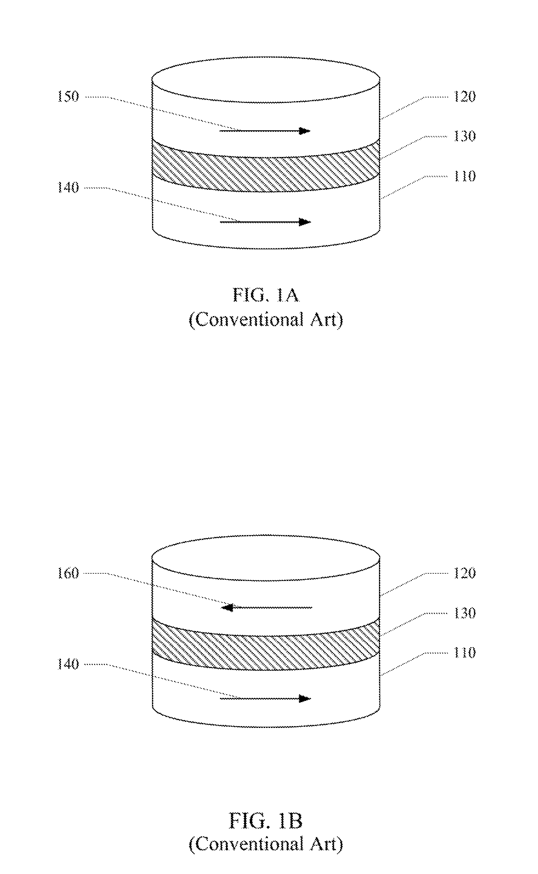
An emerging non-volatile memory technology is Magnetoresistive Random Access Memory (MRAM). In MRAM devices, data can be stored in the magnetization orientation between ferromagnetic layers of a Magnetic Tunnel Junction (MTJ). Referring to FIGS. 1A and 1B, a simplified diagram of a MTJ, in accordance with the convention art, is shown. The MTJ can include two magnetic layers 110, 120, and a magnetic tunnel barrier layer 130. One of the magnetic layers 110 can have a fixed magnetization polarization 140, while the polarization of the magnetization of the other magnetic layer 120 can switch between opposite directions 150, 160. Typically, if the magnetic layers have the same magnetization polarization 140, 150, the MTJ cell will exhibit a relatively low resistance value corresponding to a `1` bit state; while if the magnetization polarization between the two magnetic layers is antiparallel 140, 160 the MTJ cell will exhibit a relatively high resistance value corresponding to a `0` bit state. Because the data is stored in the magnetic fields, MRAM devices are non-volatile memory devices. The state of a MRAM cell can be read by applying a predetermined current through the cell and measuring the resulting voltage, or by applying a predetermined voltage across the cell and measuring the resulting current. The sensed current or voltage is proportional to the resistance of the cell and can be compared to a reference value to determine the state of the cell.
MRAM devices are characterized by densities similar to Dynamic Random-Access Memory (DRAM), power consumption similar to flash memory, and speed similar to Static Random-Access Memory (SRAM). Although MRAM devices exhibit favorable performance characteristics as compared to other memory technologies, there is a continuing need for improved MRAM devices and methods of manufacture thereof.
SUMMARY OF THE INVENTION
The present technology may best be understood by referring to the following description and accompanying drawings that are used to illustrate embodiments of the present technology directed toward methods of fabricating devices including arrays of integrated Magnetic Tunnel Junctions (MTJs) and corresponding selectors.
In one aspect, a method of manufacturing a MTJ device can include forming a plurality of source line trenches disposed in columns in a first dielectric layer. A plurality of source line conductors can be formed in the plurality of source line trenches, wherein a surface of the source line conductors are coplanar with a surface of the first dielectric layer. A second dielectric layer can be formed on the first dielectric layer and the source line conductors, and an array of selector openings can be fabricated in the second dielectric layer, wherein sets of selector openings extended to respective source line conductors. An array of selectors can be formed in the array of selector openings, wherein a surface of the selectors are coplanar with a surface of the second dielectric layer. An array of MTJ pillars coupled to the array of selectors can thereafter be formed.
In another aspect, a method of manufacturing a MTJ device can include forming a plurality of source line trenches disposed in columns in a first dielectric layer. A plurality of source line conductors can be formed in the plurality of source line trenches. A selector layer can be formed over the first dielectric layer and the plurality of source line conductors. A reference magnetic layer, a non-magnetic tunneling barrier layer, and a free magnetic layer can be formed over the selector layer. A first portion of an array of pillars can be formed from the free magnetic layer, the non-magnetic tunneling barrier layer and reference magnetic layer. A conformal dielectric layer can be formed on the exposed portions of the free magnetic layer, the non-magnetic tunnel barrier layer, and the reference magnetic layer in the first portion of the pillars and the exposed portions of the first barrier layer. A second portion of the array of pillars can be formed from the first barrier layer and the select layer, wherein portions of the conformal dielectric layer along sidewalls of the first portion of the array of pillars protect one or more of the free magnetic layer, the non-magnetic tunneling barrier layer and the reference magnetic layer during forming the second portion of the array of pillars.
This Summary is provided to introduce a selection of concepts in a simplified form that are further described below in the Detailed Description. This Summary is not intended to identify key features or essential features of the claimed subject matter, nor is it intended to be used to limit the scope of the claimed subject matter.
BRIEF DESCRIPTION OF THE DRAWINGS
Embodiments of the present technology are illustrated by way of example and not by way of limitation, in the figures of the accompanying drawings and in which like reference numerals refer to similar elements and in which:
FIGS. 1A and 1B show a simplified diagram of a MTJ, in accordance with the convention art.
FIG. 2 shows a block diagram of a cell array of a Magnetic Tunnel Junction (MTJ) device, in accordance with aspects of the present technology.
FIG. 3 shows a block diagram of a cell array of a Magnetic Tunnel Junction (MTJ) device, in accordance with aspects of the present technology.
FIG. 4 shows a block diagram of a cell array of a Magnetic Tunnel Junction (MTJ) device, in accordance with aspects of the present technology.
FIG. 5 shows a block diagram of a cell array of a Magnetic Tunnel Junction (MTJ) device, in accordance with aspects of the present technology.
FIG. 6 shows a method of fabricating a Magnetic Tunnel Junction (MTJ) device, in accordance with aspects of the present technology.
FIGS. 7A-7F illustrate method of fabricating a Magnetic Tunnel Junction (MTJ) device, in accordance with aspects of the present technology.
FIGS. 8A-8B show a method of fabricating a Magnetic Tunnel Junction (MTJ) device, in accordance with aspects of the present technology.
FIGS. 9A-9G illustrate method of fabricating a Magnetic Tunnel Junction (MTJ) device, in accordance with aspects of the present technology.
FIGS. 10A-10B show a method of fabricating a Magnetic Tunnel Junction (MTJ) device, in accordance with aspects of the present technology.
FIGS. 11A-11F illustrate method of fabricating a Magnetic Tunnel Junction (MTJ) device, in accordance with aspects of the present technology.
FIGS. 12A-12B show a method of fabricating a Magnetic Tunnel Junction (MTJ) device, in accordance with aspects of the present technology.
FIGS. 13A-13D illustrate method of fabricating a Magnetic Tunnel Junction (MTJ) device, in accordance with aspects of the present technology.
FIG. 14 shows a method of fabricating a Magnetic Tunnel Junction (MTJ) device, in accordance with aspects of the present technology.
FIGS. 15A-15D illustrate method of fabricating a Magnetic Tunnel Junction (MTJ) device, in accordance with aspects of the present technology.
FIG. 16 shows a block diagram of a cell array of a Magnetic Tunnel Junction (MTJ) device, in accordance with aspects of the present technology.
FIG. 17 shows a block diagram of a memory device, in accordance with aspects of the present technology.
FIG. 18 shows a block diagram of a computing system including a memory device, in accordance with aspects of the present technology.
FIG. 19 shows a block diagram of a computing system including a memory device, in accordance with aspects of the present technology.
FIG. 20 shows a block diagram of a memory sub-system, in accordance with aspects of the present technology.
FIG. 21 shows a block diagram of a memory sub-system, in accordance with aspects of the present technology.
DETAILED DESCRIPTION OF THE INVENTION
Reference will now be made in detail to the embodiments of the present technology, examples of which are illustrated in the accompanying drawings. While the present technology will be described in conjunction with these embodiments, it will be understood that they are not intended to limit the invention to these embodiments. On the contrary, the invention is intended to cover alternatives, modifications and equivalents, which may be included within the scope of the invention as defined by the appended claims. Furthermore, in the following detailed description of the present technology, numerous specific details are set forth in order to provide a thorough understanding of the present technology. However, it is understood that the present technology may be practiced without these specific details. In other instances, well-known methods, procedures, components, and circuits have not been described in detail as not to unnecessarily obscure aspects of the present technology.
Some embodiments of the present technology which follow are presented in terms of routines, modules, logic blocks, and other symbolic representations of operations on data within one or more electronic devices. The descriptions and representations are the means used by those skilled in the art to most effectively convey the substance of their work to others skilled in the art. A routine, module, logic block and/or the like, is herein, and generally, conceived to be a self-consistent sequence of processes or instructions leading to a desired result. The processes are those including physical manipulations of physical quantities. Usually, though not necessarily, these physical manipulations take the form of electric or magnetic signals capable of being stored, transferred, compared and otherwise manipulated in an electronic device. For reasons of convenience, and with reference to common usage, these signals are referred to as data, bits, values, elements, symbols, characters, terms, numbers, strings, and/or the like with reference to embodiments of the present technology.
It should be borne in mind, however, that all of these terms are to be interpreted as referencing physical manipulations and quantities and are merely convenient labels and are to be interpreted further in view of terms commonly used in the art. Unless specifically stated otherwise as apparent from the following discussion, it is understood that through discussions of the present technology, discussions utilizing the terms such as "receiving," and/or the like, refer to the actions and processes of an electronic device such as an electronic computing device that manipulates and transforms data. The data is represented as physical (e.g., electronic) quantities within the electronic device's logic circuits, registers, memories and/or the like, and is transformed into other data similarly represented as physical quantities within the electronic device.
In this application, the use of the disjunctive is intended to include the conjunctive. The use of definite or indefinite articles is not intended to indicate cardinality. In particular, a reference to "the" object or "a" object is intended to denote also one of a possible plurality of such objects. It is also to be understood that the phraseology and terminology used herein is for the purpose of description and should not be regarded as limiting.
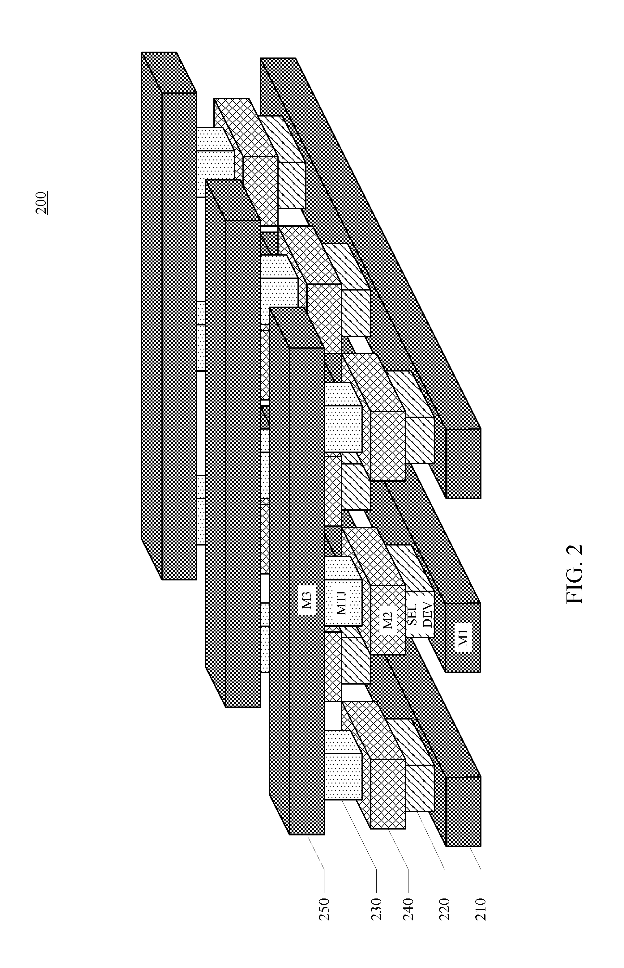
Referring to FIG. 2, a block diagram of a cell array of a Magnetic Tunnel Junction (MTJ) device, in accordance with aspects of the present technology, is shown. The MTJ device can be a Magnetoresistive Random Access Memory (MRAM), Spin Torque Magnetoresistive Random Access Memory (ST-MRAM) or similar memory device. In some aspects, the cell array 200 can include a plurality of source lines 210 disposed in columns on a wafer. In one implementation, the plurality of source lines 210 can include Copper (Cu), Tungsten (W) or other similar conductive material. For conductive material like Copper (Cu) which is characterized by a relatively high solubility and diffusivity in oxide, the plurality of source lines 210 can also include a Titanium Nitride (TiN), a Tantalum Nitride (TaN), Titanium Nitride/Tantalum Nitride (TiN/TaN) or similar capping layer. In one implementation, one or more dielectric materials can be disposed between the columns of source lines 210. In one example, the plurality of source lines 210 can be a first metalization (M1) layer.
In some aspects, the cell array 200 can include an array of selectors 220. Sets of selectors 220 can be coupled to respective source lines 210. The selectors 220 can be two-terminal elements in which the conductivity of a given selector can be controlled by the potential voltage applied across the given selector. For example, the selector 220 can be in a low resistance state when a first voltage is applied across the given selector, and the selector can be in a high resistance state when a second voltage is applied across the given selector. However, unlike the MTJ, the selector 220 does not retain a state. In one implementation, the array of selectors 220 can include a Nickel Oxide (NiOx), Titanium Oxide (TiOx), or Vanadium Oxide (VOx) or other similar material. In one implementation, one or more dielectric materials can be disposed between the array of selectors 220.
In some aspects, the cell array 200 can include an array of MTJ structures 230. The MTJ structures 230 can be coupled to respective selectors 220. The MTJ can include two magnetic layers and a magnetic tunnel barrier layer therebetween. One of the magnetic layers can have a fixed magnetization polarization, while the polarization of the magnetization of the other magnetic layer can switch between opposite directions. Typically, if the magnetic layers have the same magnetization polarization, the MTJ cell will exhibit a relatively low resistance value corresponding to a `1` bit state; while if the magnetization polarization between the two magnetic layers is antiparallel the MTJ cell will exhibit a relatively high resistance value corresponding to a `0` bit state. In one implementation, the MTJ structures 230 can include one or more first ferromagnetic layers, one or more non-magnetic layers disposed on the one or more first ferromagnetic layers, and one or more second ferromagnetic layers of a Synthetic Antiferromagnetic (SAF) portion of the MTJ. The MTJ structures 230 can also include one or more reference magnetic layers, one or more non-magnetic tunneling barrier layers disposed on the one or more reference magnetic layers, and one or more free magnetic layers disposed on the one or more non-magnetic tunneling barrier layers of a MTJ. Some or all of the one or more reference magnetic layers of the MTJ and some or all of the one or more second ferromagnetic layers of the SAF may be shared between both the MTJ and SAF portions of the MTJ structure. The MTJ structure 230 can also include one or more capping layers disposed on the free magnetic layer. In one implementation, a first ferromagnetic layer can include one or more of Cobalt (Co), Platinum (Pt), and Ruthenium (Ru), a first non-magnetic layer can include Magnesium Oxide (MgOx), a reference magnetic layer can include one or more of Cobalt (Co), Iron (Fe), and Boron (B), a non-magnetic tunneling barrier layer can include Magnesium Oxide (MgOx), and a free magnetic layer can include one or more of Cobalt (Co), Iron (Fe), Boron (B), and Tungsten (W). Each MTJ structure 230 may be implemented in a pillar, with one or more dielectric materials disposed between the array of MTJ pillars. The MTJ structures 230 can also include one or more additional layers, such as one or more seed layers, one or more anti-ferromagnetic (AFM) coupling layers, one or more ferromagnetic (FM) coupling layers, one or more Processional Spin Current (PSC) coupling layers, one or more Perpendicular Magnetic Anisotropy (PMA) layers, and the like.
In some aspects, the cell array 200 can optionally include an array of buffers 240 disposed between respective selectors 220 and respective MTJ structures 230. The array of buffers can provide a crystallization structure upon which MTJ structures 230 can be fabricate. The array of buffers can also provide a separation for the MTJ structures 230 so that the array of selectors 220 have a reduced effect on the device characteristics of the MTJ structures 230. In one implementation, the array of buffers 240 can include Tantalum Nitride (TaN) or Titanium Nitride (TiN) or similar material. In one implementation, one or more dielectric materials can be disposed between the array of buffers 240. In one example, the array of buffers 240 can be a second metalization (M2) layer. If the array of buffers 240 are not included, the plurality of source lines 230 can include Tantalum Nitride (TaN) or Titanium Nitride (TiN) or similar material.
In some aspects, the cell array 200 can include a plurality of bit lines 250 disposed in rows. The plurality of bit lines 250 can be coupled to respective sets of MTJ structures 230. In one implementation, the plurality of bit lines 250 can include Tantalum Nitride (TaN) or Titanium Nitride (TiN) or similar material. In one implementation, one or more dielectric materials can be disposed between the rows of bit lines 250. In one example, the plurality of bit lines 250 can be a third metalization (M3) layer.
The cell array 200 of the MTJ device can include numerous other layers, structures, and the like that are not germane to an understanding of aspects of the present technology. Therefore, the other layers, structures and the like of the MTJ device are not described herein.
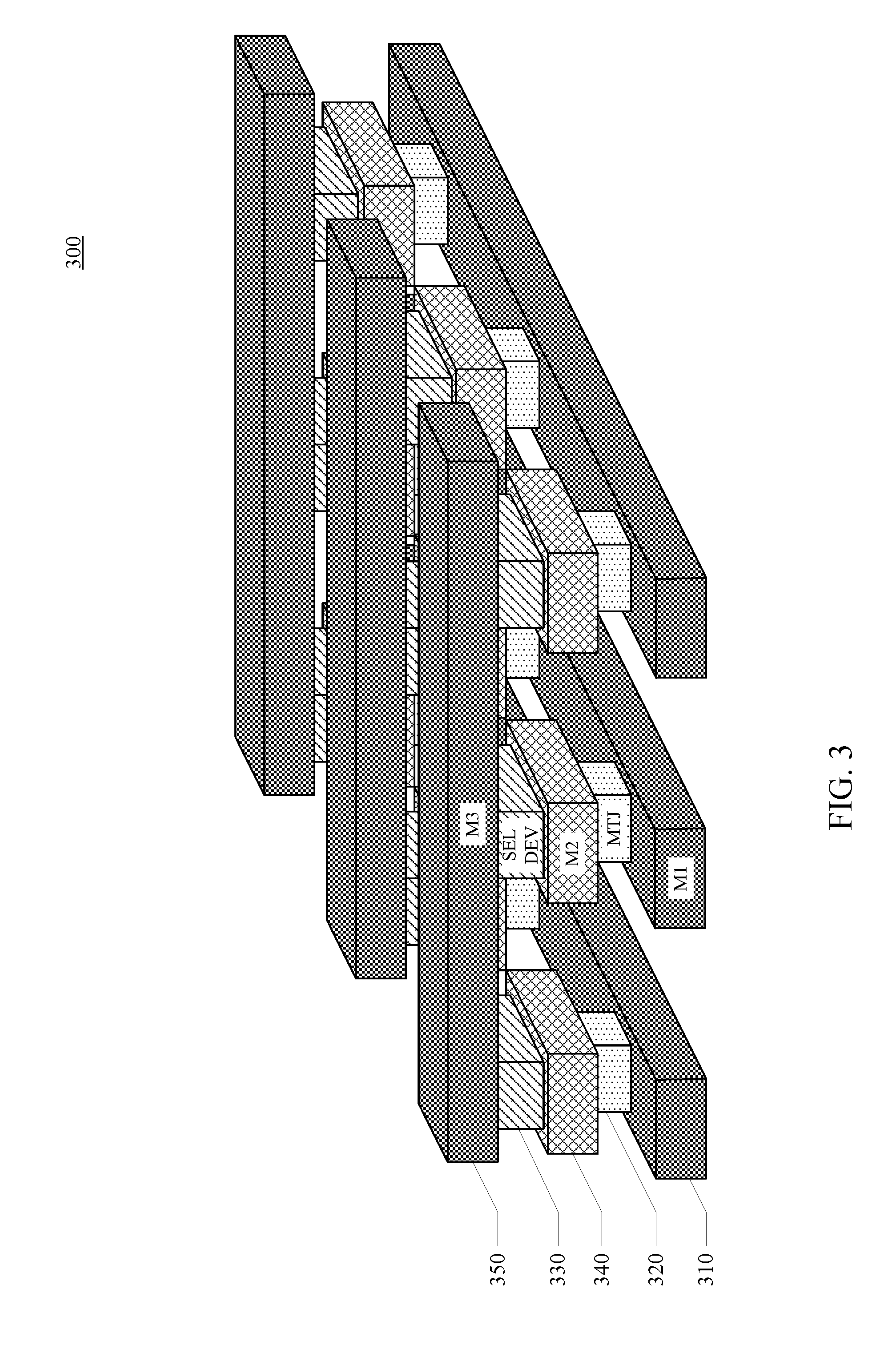
Referring now to FIG. 3 a block diagram of a cell array of a Magnetic Tunnel Junction (MTJ) device, in accordance with aspects of the present technology, is shown. The MTJ device can be a MRAM, ST-MRAM or similar memory device. In some aspects, the cell array 300 can include a plurality of bit lines 310 disposed in rows on a wafer. In one implementation, the plurality of bit lines 310 can include Copper (Cu), Tungsten (W) or other similar conductive material. For conductive material like Copper (Cu) which is characterized by a relatively high solubility and diffusivity in oxide, the plurality of bit lines 310 can also include a Titanium Nitride (TiN), a Tantalum Nitride (TaN), Titanium Nitride/Tantalum Nitride (TiN/TaN) or similar capping layer. In one implementation, one or more dielectric materials can be disposed between the rows of bit lines 310. In one example, the plurality of bit lines 310 can be a first metalization (M1) layer.
In some aspects, the cell array 300 can include an array of MTJ structures 320. Sets of the MTJ structures 320 can be coupled to respective bit lines 310. The MTJ can include two magnetic layers and a magnetic tunnel barrier layer therebetween. One of the magnetic layers can have a fixed magnetization polarization, while the polarization of the magnetization of the other magnetic layer can switch between opposite directions. Typically, if the magnetic layers have the same magnetization polarization, the MTJ cell will exhibit a relatively low resistance value corresponding to a `1` bit state; while if the magnetization polarization between the two magnetic layers is antiparallel the MTJ cell will exhibit a relatively high resistance value corresponding to a `0` bit state. In one implementation, the MTJ structures 320 can include one or more first ferromagnetic layers, one or more non-magnetic layers disposed on the one or more first ferromagnetic layers, and one or more second ferromagnetic layers of a Synthetic Antiferromagnetic (SAF) portion of the MTJ. The MTJ structures 320 can also include one or more reference magnetic layers, one or more non-magnetic tunneling barrier layers disposed on the one or more reference magnetic layers, and one or more free magnetic layers disposed on the one or more non-magnetic tunneling barrier layers of a MTJ. Some or all of the one or more reference magnetic layers of the MTJ and some or all of the one or more second ferromagnetic layers of the SAF may be shared between both the MTJ and SAF portions of the MTJ structure. The MTJ structure 320 can also include one or more capping layers disposed on the free magnetic layer. In one implementation, a first ferromagnetic layer can include one or more of Cobalt (Co), Platinum (Pt), and Ruthenium (Ru), a first non-magnetic layer can include Magnesium Oxide (MgOx), a reference magnetic layer can include one or more of Cobalt (Co), Iron (Fe), and Boron (B), a non-magnetic tunneling barrier layer can include Magnesium Oxide (MgOx), and a free magnetic layer can include one or more of Cobalt (Co), Iron (Fe), Boron (B), and Tungsten (W). Each MTJ structure 320 may be implemented in a pillar, with one or more dielectric materials disposed between the array of MTJ pillars. The MTJ structures 320 can also include one or more additional layers, such as one or more see layers, one or more anti-ferromagnetic (AFM) coupling layers, one or more ferromagnetic (FM) coupling layers, one or more Processional Spin Current (PSC) coupling layers, one or more Perpendicular Magnetic Anisotropy (PMA) layers, and the like.
In some aspects, the cell array 300 can include an array of selectors 330. The selectors 330 can be coupled to respective MTJ structures 320. The selectors 330 can be two-terminal elements in which the conductivity of a given selector can be controlled by the potential voltage applied across the given selector. For example, the selector 330 can be in a low resistance state when a first voltage is applied across the given selector, and the selector 330 can be in a high resistance state when a second voltage is applied across the given selector. In one implementation, the array of selectors 330 can include a Nickel Oxide (NiOx), Titanium Oxide (TiOx), or Vanadium Oxide (VOx) or other similar material. In one implementation, one or more dielectric materials can be disposed between the array of selectors 330.
In some aspects, the cell array 300 can optionally include an array of buffers 340 disposed between respective MTJ structures 320 and respective selectors 330. The array of buffers can provide a separation for the MTJ structures 320 so that the array of selectors 330 have a reduced effect on the device characteristics of the MTJ structures 320. In one implementation, the array of buffers 340 can include Tantalum Nitride (TaN) or Titanium Nitride (TiN) or similar material. In one implementation, one or more dielectric materials can be disposed between the array of buffers 340. In one example, the array of buffers 340 can be a second metalization (M2) layer.
In some aspects, the cell array 300 can include a plurality of source lines 350 disposed in columns. The plurality of source lines 350 can be coupled to respective sets of selectors 330. In one implementation, the plurality of source lines 350 can include Tantalum Nitride (TaN) or Titanium Nitride (TiN) or similar material. In one implementation, one or more dielectric materials can be disposed between the columns of source lines 350. In one example, the plurality of source lines 350 can be a third metalization (M3) layer.
The cell array 300 of the MTJ device can include numerous other layers, structures, and the like that are not germane to an understanding of aspects of the present technology. Therefore, the other layers, structures and the like of the MTJ device are not described herein.
As described above, the MTJ structures 230 can be disposed on top of the selectors 220, relative to the wafer, as illustrated in FIG. 2. Alternatively, the selectors 330 can be disposed on top of the MTJ structures 320, relative to the wafer, as illustrated in FIG. 3. The relative position of the MTJ structures 230, 320 and the selectors 220, 330 can be advantageous in the fabrication of the MTJ device as will be further explained with reference to the methods of manufacturing described herein.
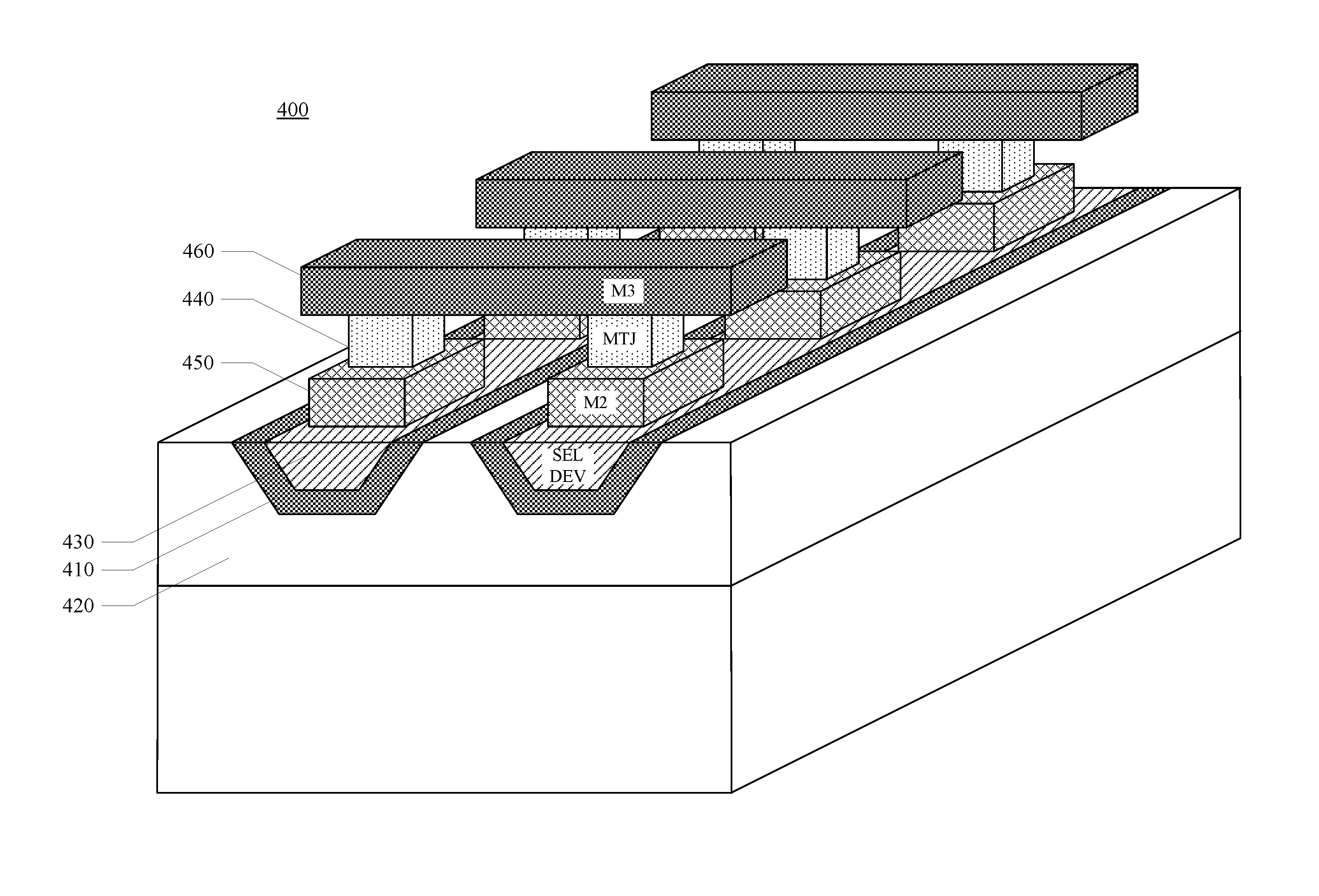
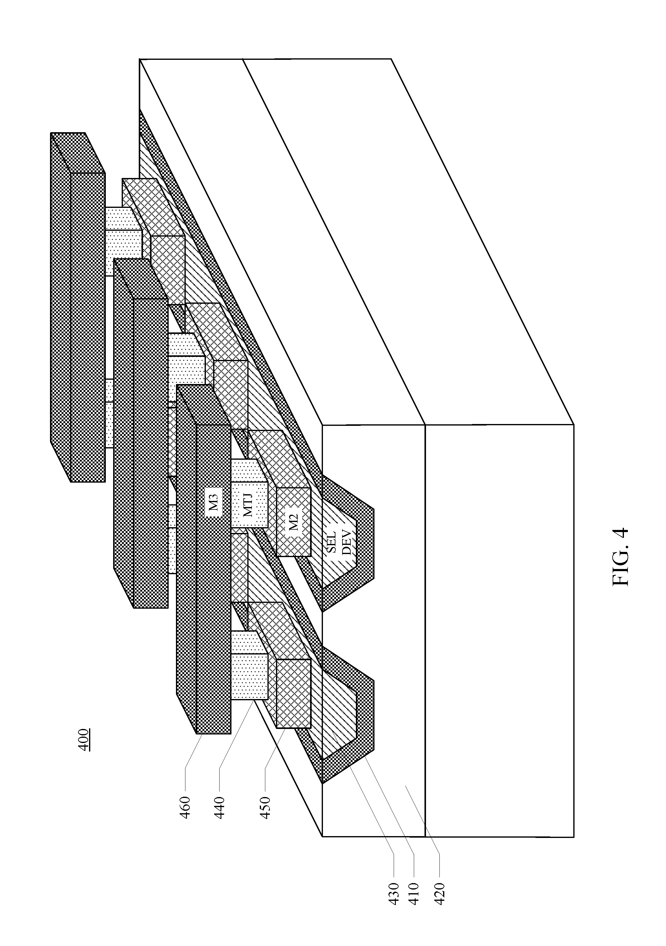
Referring now to FIG. 4, a block diagram of a cell array of a Magnetic Tunnel Junction (MTJ) device, in accordance with aspects of the present technology, is shown. The MTJ device can be a MRAM, ST-MRAM or similar memory device. In some aspects, the cell array 400 can include a plurality of source line layers 410 disposed in columns. The source line layers 410 can be disposed in corresponding trenches in a dielectric layer 420 of a wafer. In one implementation, the plurality of source line layers 410 can include Copper (Cu), Tungsten (W) or other similar conductive material. For conductive material like Copper (Cu) which is characterized by a relatively high solubility and diffusivity in oxide, the plurality of source line layers 410 can also include a Titanium Nitride (TiN), a Tantalum Nitride (TaN), Titanium Nitride/Tantalum Nitride (TiN/TaN) or similar capping layer. In one example, the plurality of source line layers 410 can be a first metalization (M1) layer.
In some aspects, the cell array 400 can include an array of selectors 430. The array of selectors 430 can be disposed on respective source line layers 410 in the corresponding trenches in the dielectric layer 420. The selectors 430 can be two-terminal elements in which the conductivity of a given selector can be controlled by the potential voltage applied across the given selector. For example, the selector 430 can be in a low resistance state when a first voltage is applied across the given selector, and the selector 430 can be in a high resistance state when a second voltage is applied across the given selector. In one implementation, the array of selectors 430 can include a Nickel Oxide (NiOx), Titanium Oxide (TiOx), or Vanadium Oxide (VOx) or other similar material. In some aspects, a surface of the source line layers 410, and a surface of the selectors 430 can be coplanar with a surface of the dielectric layer 420.
In some aspects, the cell array 400 can include an array of MTJ structures 440. The MTJ structures 440 can be coupled to respective selectors 430. The MTJ structure 440 can include two magnetic layers and a magnetic tunnel barrier layer therebetween. One of the magnetic layers can have a fixed magnetization polarization, while the polarization of the magnetization of the other magnetic layer can switch between opposite directions. Typically, if the magnetic layers have the same magnetization polarization, the MTJ cell will exhibit a relatively low resistance value corresponding to a `1` bit state; while if the magnetization polarization between the two magnetic layers is antiparallel the MTJ cell will exhibit a relatively high resistance value corresponding to a `0` bit state. In one implementation, the MTJ structures 440 can include one or more first ferromagnetic layers, one or more non-magnetic layers disposed on the one or more first ferromagnetic layers, and one or more second ferromagnetic layers of a Synthetic Antiferromagnetic (SAF) portion of the MTJ. The MTJ structures 230 can also include one or more reference magnetic layers, one or more non-magnetic tunneling barrier layers disposed on the one or more reference magnetic layers, and one or more free magnetic layers disposed on the one or more non-magnetic tunneling barrier layers of a MTJ. Some or all of the one or more reference magnetic layers of the MTJ and some or all of the one or more second ferromagnetic layers of the SAF may be shared between both the MTJ and SAF portions of the MTJ structure. The MTJ structure 440 can also include one or more capping layers disposed on the free magnetic layer. In one implementation, a first ferromagnetic layer can include one or more of Cobalt (Co), Platinum (Pt), and Ruthenium (Ru), a first non-magnetic layer can include Magnesium Oxide (MgOx), a reference magnetic layer can include one or more of Cobalt (Co), Iron (Fe), and Boron (B), a non-magnetic tunneling barrier layer can include Magnesium Oxide (MgOx), and a free magnetic layer can include one or more of Cobalt (Co), Iron (Fe), Boron (B), and Tungsten (W). Each MTJ structure 40 may be implemented in a pillar, with one or more dielectric materials (not shown) disposed between the array of MTJ pillars. The MTJ structures 440 can also include one or more additional layers, such as one or more seed layers, one or more anti-ferromagnetic (AFM) coupling layers, one or more ferromagnetic (FM) coupling layers, one or more Processional Spin Current (PSC) coupling layers, one or more Perpendicular Magnetic Anisotropy (PMA) layers, and the like.
In some aspects, the cell array 400 can optionally include an array of buffers 450 disposed between respective selectors 430 and respective MTJ structures 440. The array of buffers 450 can provide a crystallization structure upon which MTJ structures 440 can be fabricate. The array of buffers 450 can also provide a separation for the MTJ structures 440 so that the array of selectors 430 have a reduced effect on the device characteristics of the MTJ structures 230. In one implementation, the array of buffers 450 can include Tantalum Nitride (TaN) or Titanium Nitride (TiN) or similar material. In one implementation, one or more dielectric materials (not shown) can be disposed between the array of buffers 450. I n one example, the array of buffers 450 can be a second metalization (M2) layer.
In some aspects, the cell array 400 can include a plurality of bit lines 460 disposed in rows. The plurality of bit lines 460 can be coupled to respective sets of MTJ structures 440. In one implementation, the plurality of bit lines 460 can include Tantalum Nitride (TaN) or Titanium Nitride (TiN) or similar material. In one implementation, one or more dielectric materials (not shown) can be disposed between the rows of bit lines 460. In one example, the plurality of bit lines 460 can be a third metalization (M3) layer.
The cell array 400 of the MTJ device can include numerous other layers, structures, and the like that are not germane to an understanding of aspects of the present technology. Therefore, the other layers, structures and the like of the MTJ device are not described herein.
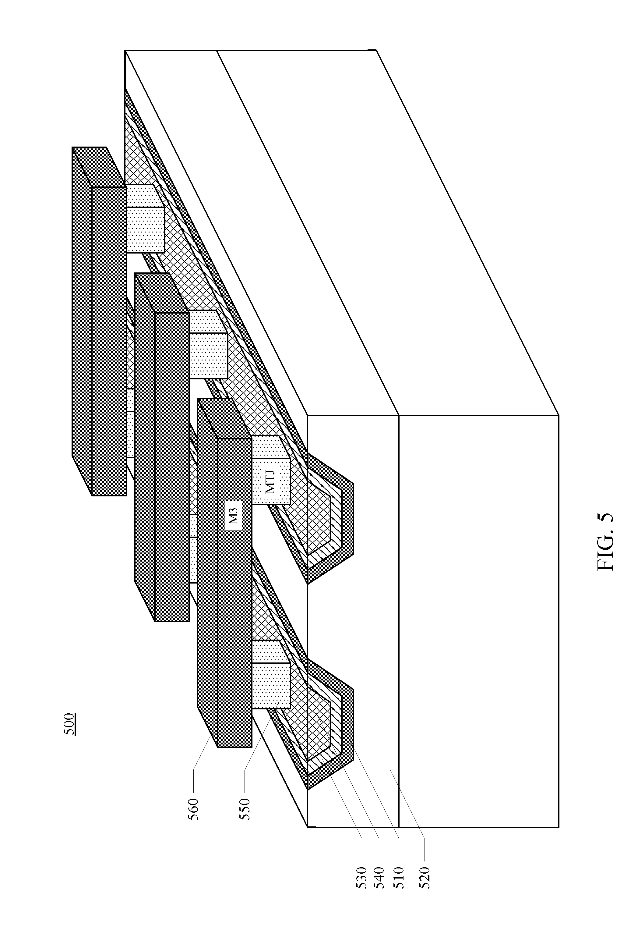
Referring now to FIG. 5, a block diagram of a cell array of a Magnetic Tunnel Junction (MTJ) device, in accordance with aspects of the present technology, is shown. The MTJ device can be a MRAM, ST-MRAM or similar memory device. In some aspects, the cell array 500 can include a plurality of source line layers 410 disposed in columns. The source line layers 510 can be disposed in corresponding trenches in a dielectric layer 520 of a wafer. In one implementation, the plurality of source line layers 510 can include Copper (Cu), Tungsten (W) or other similar conductive material. For conductive material like Copper (Cu) which is characterized by a relatively high solubility and diffusivity in oxide, the plurality of source line layers 510 can also include a Titanium Nitride (TiN), a Tantalum Nitride (TaN), Titanium Nitride/Tantalum Nitride (TiN/TaN) or similar capping layer. In one example, the plurality of source line layers 510 can be a first metalization (M1) layer.
In some aspects, the cell array 500 can include an array of selectors 530. The array of selectors 530 can be disposed on respective source line layers 510 in the corresponding trenches in the dielectric layer 520. The selectors 530 can be two-terminal elements in which the conductivity of a given selector can be controlled by the potential voltage applied across the given selector. For example, the selector 530 can be in a low resistance state when a first voltage is applied across the given selector, and the selector can be in a high resistance state when a second voltage is applied across the given selector. In one implementation, the array of selectors 530 can include a Nickel Oxide (NiOx), Titanium Oxide (TiOx), or Vanadium Oxide (VOx) or other similar material.
In some aspects, the cell array 500 can include an array of buffers 540 disposed one respective selectors 530 in the corresponding trenches in the dielectric layer 520. The array of buffers 540 can provide a crystallization structure upon which MTJ structures 550 can be fabricate. The array of buffers 540 can also provide a separation for the MTJ structures 550 so that the array of selectors 530 have a reduced effect on the device characteristics of the MTJ structures 550. In one implementation, the array of buffers 540 can include Tantalum Nitride (TaN) or Titanium Nitride (TiN) or similar material. In one example, the array of buffers 540 can be a second metalization (M2) layer. In some aspects, a surface of the source line layers 410, a surface of the selectors 430 and a surface of the buffers 540 can be coplanar with a surface of the dielectric layer 520.
In some aspects, the cell array 500 can include an array of MTJ structures 550. The MTJ structures 550 can be coupled to respective buffers 540. The MTJ can include two magnetic layers and a magnetic tunnel barrier layer therebetween. One of the magnetic layers can have a fixed magnetization polarization, while the polarization of the magnetization of the other magnetic layer can switch between opposite directions. Typically, if the magnetic layers have the same magnetization polarization, the MTJ cell will exhibit a relatively low resistance value corresponding to a `1` bit state; while if the magnetization polarization between the two magnetic layers is antiparallel the MTJ cell will exhibit a relatively high resistance value corresponding to a `0` bit state. In one implementation, the MTJ structures 550 can include one or more first ferromagnetic layers, one or more non-magnetic layers disposed on the one or more first ferromagnetic layers, and one or more second ferromagnetic layers of a Synthetic Antiferromagnetic (SAF) portion of the MTJ. The MTJ structures 230 can also include one or more reference magnetic layers, one or more non-magnetic tunneling barrier layers disposed on the one or more reference magnetic layers, and one or more free magnetic layers disposed on the one or more non-magnetic tunneling barrier layers of a MTJ. Some or all of the one or more reference magnetic layers of the MTJ and some or all of the one or more second ferromagnetic layers of the SAF may be shared between both the MTJ and SAF portions of the MTJ structure. The MTJ structure 550 can also include one or more capping layers disposed on the free magnetic layer. In one implementation, a first ferromagnetic layer can include one or more of Cobalt (Co), Platinum (Pt), and Ruthenium (Ru), a first non-magnetic layer can include Magnesium Oxide (MgOx), a reference magnetic layer can include one or more of Cobalt (Co), Iron (Fe), and Boron (B), a non-magnetic tunneling barrier layer can include Magnesium Oxide (MgOx), and a free magnetic layer can include one or more of Cobalt (Co), Iron (Fe), Boron (B), and Tungsten (W). Each MTJ structure 550 may be implemented in a pillar, with one or more dielectric materials (not shown) disposed between the array of MTJ pillars. The MTJ structures 550 can also include one or more additional layers, such as one or more see layers, one or more anti-ferromagnetic (AFM) coupling layers, one or more ferromagnetic (FM) coupling layers, one or more Processional Spin Current (PSC) coupling layers, one or more Perpendicular Magnetic Anisotropy (PMA) layers, and the like.
In some aspects, the cell array 500 can include a plurality of bit lines 560 disposed in rows. The plurality of bit lines 560 can be coupled to respective sets of MTJ structures 550. In one implementation, the plurality of bit lines 560 can include Tantalum Nitride (TaN) or Titanium Nitride (TiN) or similar material. In one implementation, one or more dielectric materials (not shown) can be disposed between the rows of bit lines 560. In one example, the plurality of bit lines 560 can be a third metalization (M3) layer.
The cell array 400 of the MTJ device can include numerous other layers, structures, and the like that are not germane to an understanding of aspects of the present technology. Therefore, the other layers, structures and the like of the MTJ device are not described herein.
In some aspects, the cell array 200, 300, 400 of the MTJ devices can advantageously be stacked on top of each other to implement vertical three-dimension (3D) memory architectures, such as cross-point MRAM, cross-point ST-MRAM and the like.
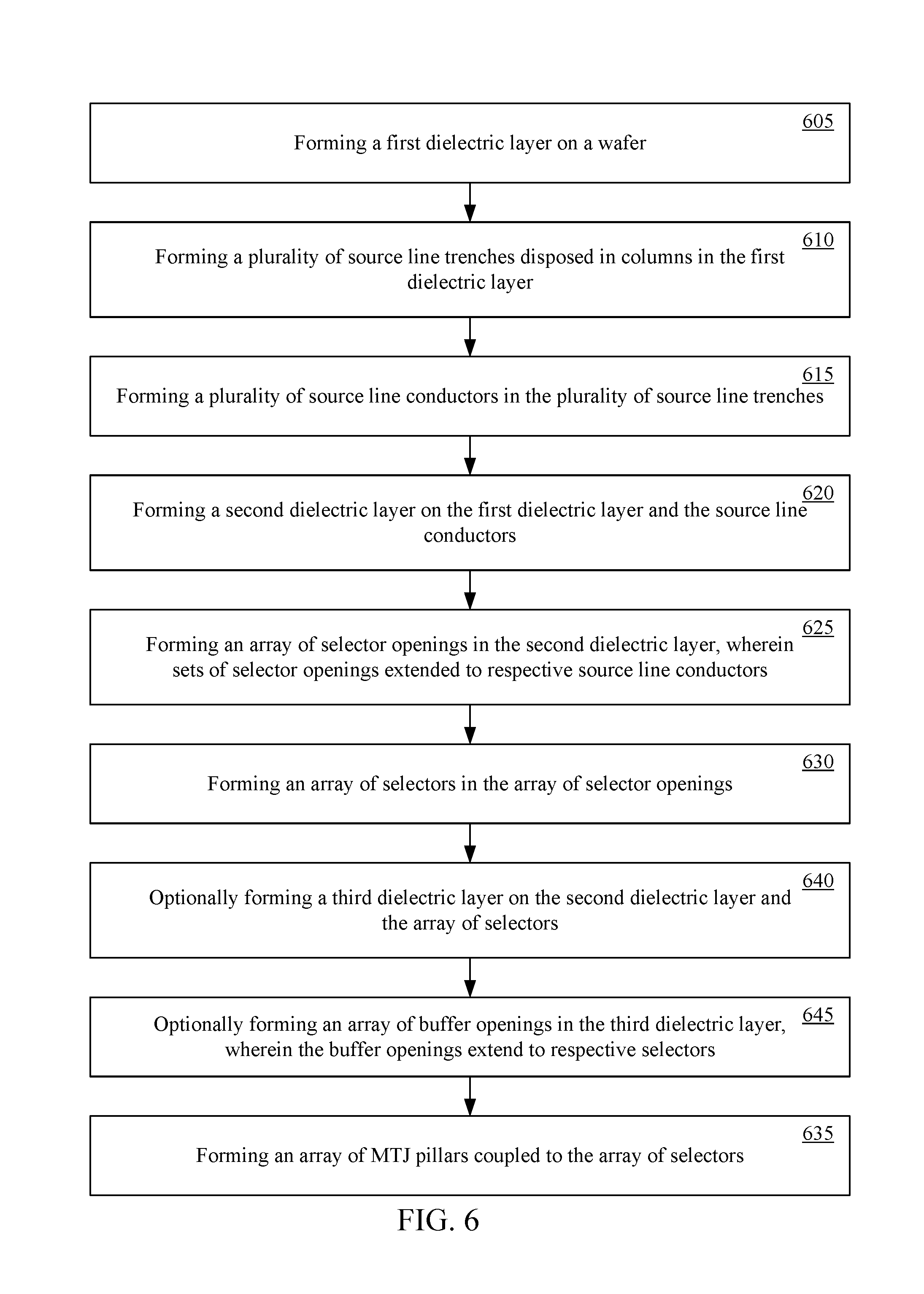
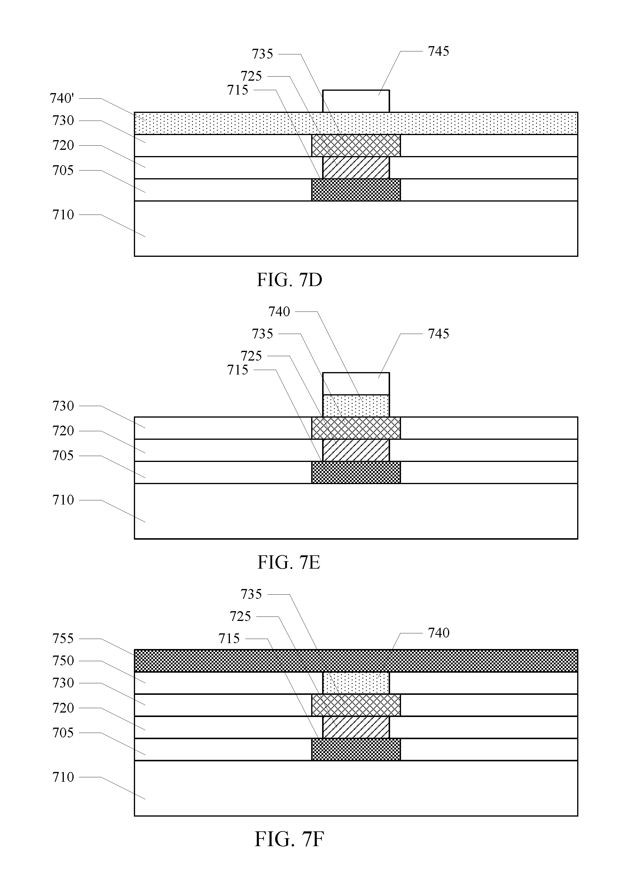
Referring now to FIG. 6, a method of fabricating a Magnetic Tunnel Junction (MTJ) device, in accordance with aspects of the present technology, is shown. The method of fabrication will be described with reference to FIGS. 7A-7F, which illustrate the method of fabrication. The MTJ device can be a Magnetoresistive Random Access Memory (MRAM), Spin Torque Magnetoresistive Random Access Memory (ST-MRAM) or similar memory device. In some aspects, a first dielectric layer 705 can be formed on a wafer 710, at 605. In one implementation, forming the first dielectric layer can include depositing a layer of Silicon Oxide (SiO), Silicon Nitride (SiN) or other similar material, with a thickness of approximately 10-100 nanometers (nm), by a process such as Chemical Vapor Deposition (CVD), Atomic Layer Deposition (ALD), Physical Vapor Deposition (PVD) or Plasma Enhanced Chemical Vapor Deposition or the like.
In some aspects, a plurality of source line trenches can be formed in columns in the first dielectric layer, at 610. In one implementation, the plurality of source line trenches can be formed by selectively etching the first dielectric layer exposed by a source line trench mask.
In some aspects, a plurality of source line conductors 715 can be formed in the plurality of source line trenches, at 615. In one implementation, forming the plurality of source line conductors can include depositing a first conductive layer 715' on the first dielectric layer 705 and filling the plurality of source line trenches. The first conductive layer can be Copper (Cu), Tungsten (W) or other similar conductor deposited by a process such as Physical Vapor Deposition (PVD), Atomic Layer Deposition (ALC) or the like. In addition, a first liner layer can be deposited on the first dielectric layer including the plurality of source line trenches before depositing the first conductive layer. For conductive material like Copper (Cu) which is characterized by a relatively high solubility and diffusivity in oxide, the first liner layer can be Titanium Nitride (TiN), Tantalum Nitride (TaN), Titanium Nitride/Tantalum Nitride (TiN/TaN) or similar material with a thickness of approximately 5-15 nm, by a process such as High-Density Plasma (HDP) deposition or the like. The first conductive layer can then be Chemical-Mechanical Polished (CMP) to remove the first conductive layer on the first dielectric layer and leaving the first conductive layer material in the plurality of source line trenches to form the plurality of source line conductors with a thickness of approximately 100-150 nm. The liner layer on the first dielectric layer can be utilized as a CMP stop. A surface of the source line conductors can be formed to be coplanar with a surface of the first dielectric layer as a result of the CMP process. In addition, a first capping layer can be deposited on the plurality first source line conductors after the CMP process. The first capping layer can be deposited by a process such as electroplating or the like. The first capping layer can be Titanium Nitride (TiN), Tantalum Nitride (TaN), Titanium Nitride/Tantalum Nitride (TiN/TaN) or similar material with a thickness of approximately 5-15 nm, to reduce solubility and diffusivity of the first source line conductor material into the first dielectric layer and other subsequently formed layers. The first capping layer material and thickness can be selected based upon a filing characteristic of the subsequent deposition of selector layer in the array of selector elements, and/or the CMP selectivity of the selector material over the capping layer material.
In some aspects, a second dielectric layer 720 can be formed on the first dielectric layer and the source line conductors, at 620. In one implementation, the second dielectric layer can be deposited on the first dielectric layer and the source line conductors by a process such as Chemical Vapor Deposition (CVD), Atomic Layer Deposition (ALD), Physical Vapor Deposition (PVD) or Plasma Enhanced Chemical Vapor Deposition or the like. The second dielectric layer can be Silicon Oxide (SiO), Silicon Nitride (SiN) with a thickness of approximately about 50 nm.
In some aspects, an array of selector openings can be formed in the second dielectric layer, at 625. Sets of the selector opening can extended to respective source line conductors. In one implementation, the array of selector openings can be formed by selectively etching the second dielectric layer exposed by a selector opening mask.
In some aspects, an array of selectors 725 can be formed in the selector openings 630. In one implementation, forming the array of selectors can include depositing a selector layer 725' on the second dielectric layer and filling the array of selector openings. The selector layer can be a Nickel Oxide (NiOx), Titanium Oxide (TiOx), or Vanadium Oxide (VOx) or other similar material deposited by a process such as sputtering or the like. Sputtering of the selector material can be performed in the presence of a strong electromagnetic fields to confine charge plasma particles close to the surface of the plurality of source line conductor targets. Depending on a design current density and rectifying ratio, the thickness of the selector material can composition of the selector material can be tuned and modified. Post-deposition morphology may not be smooth due to the via structure of the selector. The selector layer can then be CMP to remove the selector layer on the second dielectric layer and leaving the selector layer material in the array of selector opening to form the array of selectors with a thickness of approximately 30-50 nm. The slurry, pad pressure and speed can be selected to achieve a good selective removal rate of the selector material over the second dielectric material. The good selectivity can minimize loss of stack height. A surface of the selectors can be coplanar with a surface of the second dielectric layer as a result of the CMP process. In addition, a second capping layer can be deposited on the array of selectors after the CMP process. The second capping layer can be deposited by a process such as electroplating or the like. The second capping layer can be Titanium Nitride (TiN), Tantalum Nitride (TaN), Titanium Nitride/Tantalum Nitride (TiN/TaN) or similar material with a thickness of approximately 5-70 nm, to reduce solubility and diffusivity of the selector material into the second dielectric layer and other subsequently formed layers.
In some aspects, an optional third dielectric layer 730 can be formed on the second dielectric layer and the array of selectors, at 635. In one implementation, the third dielectric layer can be deposited on the second dielectric layer and the array of selectors by a process such as Chemical Vapor Deposition (CVD), Atomic Layer Deposition (ALD), Physical Vapor Deposition (PVD) or Plasma Enhanced Chemical Vapor Deposition or the like. The third dielectric layer can be Silicon Oxide (SiO), Silicon Nitride (SiN) with a thickness of approximately 40-60 nm.
In some aspects, optionally an array of buffer opening in the third dielectric layer can be formed, at 640. The buffer openings can extend to respective selectors. In one implementation, the array of buffer openings can be formed by selectively etching the third dielectric layer exposed by a buffer opening mask.
In some aspects, an optional array of buffers 735 can be formed in the array of buffer openings when the optional array of buffer openings are formed in the optional third dielectric layer, at 645. In one implementation, forming the array of buffers can include depositing a buffer layer 735' on the third dielectric layer and filling the array of buffer openings. The buffer layer can be Tantalum Nitride (TaN) or other similar material deposited by a process such as High-Density Plasma (HDP) deposition or the like. The buffer layer can then be CMP to remove the buffer layer on the third dielectric layer and leaving the buffer layer material in the array of buffer opening to form the array of buffers with a thickness of approximately 50 nm. A surface of the buffers can be coplanar with a surface of the third dielectric layer as a result of the CMP process. Forming array of buffers before forming the array of MTJs advantageously allows the fabrication of the MTJs without the processes used for forming the selectors affecting the performance parameters of the MTJs.
In some aspects, an array of MTJ pillars 740 can be formed, at 650. The MTJ pillars can be coupled directly to the array of selectors, or through the array of optional buffers to the array of selectors. In one implementation, a reference magnetic layer can be formed over the first barrier layer. A non-magnetic tunneling barrier layer can be formed over the reference magnetic layer. A free magnetic layer can be formed over the non-magnetic tunneling barrier layer. An array of pillars can be formed from the free magnetic layer, the non-magnetic tunnel barrier layer, and the reference magnetic layer by selective etching the free magnetic layer, the non-magnetic tunnel barrier layer, and the reference magnetic layer exposed by one or more pillar masks 745.
Fabrication can continue with forming a fourth dielectric layer 750 and forming a plurality of bit lines 755 disposed in rows and coupled to the MTJ pillars 740. The fabrication of the MTJ device can include numerous other processes that are not germane to an understanding of aspect of the present technology. Therefore, the other processes of fabricating the MTJ device are not described herein.
In some aspects, multiple cell arrays can be fabricated in stacks on top of each other to implement vertical three-dimension (3D) memory architectures, such as cross-point MRAM, cross-point ST-MRAM and the like. The stacked arrays can be formed by repeating the above described processes to form multiple cell arrays stacked upon each other.
Referring now to FIGS. 8A-8B, a method of fabricating a Magnetic Tunnel Junction (MTJ) device, in accordance with aspects of the present technology, is shown. The method of fabrication will be described with reference to FIGS. 9A-9G, which illustrate the method of fabrication. The MTJ device can be a MRAM, ST-MRAM or similar memory device. In some aspects, a first dielectric layer 905 can be formed on a wafer 910, at 805. In one implementation, forming the first dielectric layer can include depositing a layer of Silicon Oxide (SiO), Silicon Nitride (SiN) or other similar material, with a thickness of approximately 40-60 nm, by a process such as Chemical Vapor Deposition (CVD), Atomic Layer Deposition (ALD), Physical Vapor Deposition (PVD) or Plasma Enhanced Chemical Vapor Deposition or the like.
In some aspects, a plurality of source line trenches can be formed in columns in the first dielectric layer, at 810. In one implementation, the plurality of source line trenches can be formed by selectively etching the first dielectric layer exposed by a source line trench mask.
In some aspect, a plurality of source line conductors 915 can be formed in the plurality of source line trenches, at 815. In one implementation, forming the plurality of source line conductors can include depositing a first conductive layer 915' on the first dielectric layer 905 and filling the plurality of source line trenches. The first conductive layer can be Copper (Cu), Tungsten (W) or other similar conductor deposited by a process such as ??? or the like. In addition, a first liner layer can be deposited on the first dielectric layer including the plurality of source line trenches before depositing the first conductive layer. For conductive material like Copper (Cu) which is characterized by a relatively high solubility and diffusivity in oxide, the first liner layer can be Titanium Nitride (TiN), Tantalum Nitride (TaN), Titanium Nitride/Tantalum Nitride (TiN/TaN) or similar material with a thickness of approximately 5-15 nm, by a process such as High-Density Plasma (HDP) deposition or the like. The first conductive layer can then be Chemical-Mechanical Polished (CMP) to remove the first conductive layer on the first dielectric layer and leaving the first conductive layer material in the plurality of source line trenches to form the plurality of source line conductors with a thickness of approximately 100-150 nm. The liner layer on the first dielectric layer can be utilized as a CMP stop. A surface of the source line conductors can be formed to be coplanar with a surface of the first dielectric layer as a result of the CMP process. In addition, a first capping layer can be deposited on the plurality source line conductors after the CMP process. The first capping layer can be deposited by a process such as electroplating or the like. The first capping layer can be Titanium Nitride (TiN), Tantalum Nitride (TaN), Titanium Nitride/Tantalum Nitride (TiN/TaN) or similar material with a thickness of approximately 5-15 nm, to reduce solubility and diffusivity of the source line conductor material into the first dielectric layer and other subsequently formed layers. The first capping layer material and thickness can be selected based upon a filing characteristic of the subsequent deposition of selector layer in the array of selector elements, and/or the CMP selectivity of the selector material over the capping layer material.
In some aspects, a selector layer 920' can be formed over the first dielectric layer and the plurality of source line conductors, at 820. In one implementation, the selector layer can be formed by depositing a layer of Nickel Oxide (NiOx), Titanium Oxide (TiOx), or Vanadium Oxide (VOx) or other similar material, with a thickness of approximately 50 nm, by a process such as sputtering or the like. Sputtering of the selector material can be performed in the presence of a strong electromagnetic fields to confine charge plasma particles close to the surface of the target. Depending on a design current density and rectifying ratio, the thickness of the selector material can composition of the selector material can be tuned and modified. Post-deposition morphology may not be smooth due to the via structure of the selector.
In some aspects, a first buffer layer 925' can be formed on the selector layer, at 825. In one implementation, the buffer layer can be formed by deposit a layer of Tantalum Nitride (TaN) or other similar material, with a thickness of approximately 50-100 nm, by a process such as High-Density Plasma (HDP) deposition or the like. The array of buffers disposed between the array of selectors and the subsequently formed array of MTJs advantageously allow the fabrication of the MTJs without the processes used for forming the selectors affecting the performance parameters of the MTJs.
In some aspects, a reference magnetic layer can be formed over the first barrier layer, 830. In one implementation, the reference magnetic layer can be formed by depositing a layer of Cobalt-Iron-Boron (Co--Fe--B) alloy or other similar material, with a thickness of approximately 1-5 nm, by a process such as Physical Vapor Deposition (PVD) or the like.
In some aspects, a non-magnetic tunneling barrier layer can be formed over the reference magnetic layer, at 835. In one implementation, the non-magnetic tunneling barrier layer can be formed by depositing a layer of Magnesium Oxide (MgOx) or other similar material, with a thickness of approximately 0.1-1 nm, by a process such as sputtering or the like.
In some aspects, a free magnetic layer can be formed over the non-magnetic tunneling barrier layer, at 840. In one implementation, the free magnetic layer can be formed by depositing a layer of Cobalt-Iron-Boron (Co--Fe--B) alloy or other similar material, with a thickness of approximately 0.5-2 nm, by a process such as Physical Vapor Deposition (PVD) or the like.
In some aspects, a first portion of an array of pillars 930 can be formed from the free magnetic layer, the non-magnetic tunnel barrier layer, and the reference magnetic layer, at 845. In one implementation, the first portion of the array of pillars can be formed by selectively etching the free magnetic layer, the non-magnetic tunnel barrier layer, and the reference magnetic layer exposed by one or more pillar masks 935.
In some aspects, a conformal dielectric layer 945' can be formed on the exposed portion of the free magnetic layer, the non-magnetic tunnel barrier layer, and the reference magnetic layer in the first portion of the pillars and the exposed portion of the first barrier layer, at 850. In one implementation, the conformal dielectric layer can be formed by depositing a layer of Silicon Oxide (SiO), Silicon Nitride (SiN) or other similar material, with a thickness of approximately 50 nm, by a process such as Chemical Vapor Deposition (CVD), Atomic Layer Deposition (ALD), Physical Vapor Deposition (PVD) or Plasma Enhanced Chemical Vapor Deposition or the like.
In some aspects, a second portion of the array of pillars can be formed from the first barrier layer and the select layer, at 855. In one implementation, portions of the conformal dielectric layer 940' on the exposed portion of the first barrier layer, the exposed portions of the barrier layer 925, and the exposed portions of the select layer 920 can be selectively etched to form the second portion of the array of pillars. Portions of the conformal dielectric layer 940 along sidewalls of the first portion of the array of pillars can protect one or more of the free magnetic layer, the non-magnetic tunneling barrier layer and the reference magnetic layer during forming the second portion of the array of pillars. The dielectric layer 940 along the sidewalls of the first portion of the array of pillars can prevent re-deposition of the barrier layer and/or select layer on the free magnetic, the non-magnetic tunnel barrier layer, and/or the reference magnetic layer, and/or contamination thereof during the etching process.
Fabrication can continue with forming a second dielectric layer 945 and forming a plurality of bit lines 950 disposed in rows and coupled to the MTJ pillars 930. The fabrication of the MTJ device can include numerous other processes that are not germane to an understanding of aspect of the present technology. Therefore, the other processes of fabricating the MTJ device are not described herein.
In some aspects, multiple cell arrays can be fabricated in stacks on top of each other to implement vertical three-dimension (3D) memory architectures, such as cross-point MRAM, cross-point ST-MRAM and the like. The stacked arrays can be formed by repeating the above described processes to form multiple cell arrays stacked upon each other.
Referring now to FIGS. 10A-10B, a method of fabricating a Magnetic Tunnel Junction (MTJ) device, in accordance with aspects of the present technology, is shown. The method of fabrication will be described with reference to FIGS. 11A-11F, which illustrate the method of fabrication. The MTJ device can be a Magnetoresistive Random Access Memory (MRAM), Spin Torque Magnetoresistive Random Access Memory (ST-MRAM) or similar memory device. In some aspect, a first dielectric layer 1105 can be formed on a wafer 1110, at 1005. In one implementation, forming the first dielectric layer can include depositing a layer of Silicon Oxide (SiO), Silicon Nitride (SiN) or other similar material, with a thickness of approximately 40-60 nm, by a process such as Chemical Vapor Deposition (CVD), Atomic Layer Deposition (ALD), Physical Vapor Deposition (PVD) or Plasma Enhanced Chemical Vapor Deposition or the like.
In some aspects, a plurality of trenches can be formed in columns in the first dielectric layer, at 1010. In one implementation, the plurality of trenches can be formed by selectively etching the first dielectric layer exposed by a trench mask.
In some aspects, a source line layer 1115' can be formed on the first dielectric layer including in the plurality of trenches, at 1015. In one implementation, forming the first source line layer can include depositing a layer of Copper (Cu), Tungsten (W) or other similar material, with a thickness of approximately 100-150 nm, by a process such as Atomic Layer Deposition (ALD) or the like.
In some aspects, a select layer 1120' can be formed on the source line layer including in the plurality of trenches, at 1020. In one implementation, the selector layer can be formed by depositing a layer of Nickel Oxide (NiOx), Titanium Oxide (TiOx), or Vanadium Oxide (VOx) or other similar material, with a thickness of approximately 50 nm, by a process such as sputtering or the like. Sputtering of the selector material can be performed in the presence of a strong electromagnetic fields to confine charge plasma particles close to the surface of the target. Depending on a design current density and rectifying ratio, the thickness of the selector material can composition of the selector material can be tuned and modified. Post-deposition morphology may not be smooth due to the via structure of the selector.
In some aspects, the select layer 1115' and the source line layer 1120' can be planarized to remove the selector layer and the source line layer on the first dielectric layer and leaving selector layer material and source line layer material in the plurality of trenches 1025. In one implementation, the select layer and the source line layer can be CMPed to remove the selector layer and the source line layer on the first dielectric layer and leaving selector layer material and source line layer material in the plurality of trenches. After CMPing the portions of the selectors, the source lines and the first dielectric layer can be coplanar.
In some aspects, a first barrier layer can be formed on the coplanar exposed portions of the select layer, source line layer and first dielectric layer, at 1030. In one implementation, the first barrier layer can be formed by deposit a layer of Tantalum Nitride (TaN) or other similar material, with a thickness of approximately 50-100 nm, by a process such as High-Density Plasma (HDP) deposition or the like.
In some aspects, a reference magnetic layer can be formed over the first barrier layer, 1035. In one implementation, the reference magnetic layer can be formed by depositing a layer of Cobalt-Iron-Boron (Co--Fe--B) alloy or other similar material, with a thickness of approximately 1-5 nm, by a process such as Physical Vapor Deposition (PVD) or the like.
In some aspects, a non-magnetic tunneling barrier layer can be formed over the reference magnetic layer, at 1040. In one implementation, the non-magnetic tunneling barrier layer can be formed by depositing a layer of Magnesium Oxide (MgOx) or other similar material, with a thickness of approximately 0.1-1 nm, by a process such as sputtering or the like.
In some aspects, a free magnetic layer can be formed over the non-magnetic tunneling barrier layer, at 1045. In one implementation, the free magnetic layer can be formed by depositing a layer of Cobalt-Iron-Boron (Co--Fe--B) alloy or other similar material, with a thickness of approximately 0.5-2 nm, by a process such as Physical Vapor Deposition (PVD) or the like.
In some aspects, a first portion of an array of pillars 1050 can be formed from the free magnetic layer, the non-magnetic tunnel barrier layer, and the reference magnetic layer, at 1050. In one implementation, the first portion of the array of pillars can be formed by selectively etching the free magnetic layer, the non-magnetic tunnel barrier layer, and the reference magnetic layer exposed by one or more pillar masks.
In some aspects, a conformal dielectric layer 1155 can be formed on the exposed portion of the free magnetic layer, the non-magnetic tunnel barrier layer, and the reference magnetic layer in the first portion of the pillars and the exposed portion of the first barrier layer, at 1055. In one implementation, the conformal dielectric layer can be formed by depositing a layer of Silicon Oxide (SiO), Silicon Nitride (SiN) or other similar material, with a thickness of approximately 50 nm, by a process such as Chemical Vapor Deposition (CVD), Atomic Layer Deposition (ALD), Physical Vapor Deposition (PVD) or Plasma Enhanced Chemical Vapor Deposition or the like.
In some aspects, a second portion of the array of pillars 1160 can be formed from the first barrier layer and the select layer, at 1060. In one implementation, portions of the conformal dielectric layer on the exposed portion of the first barrier layer, the exposed portions of the barrier layer, and the exposed portions of the select layer can be selectively etched to form the second portion of the array of pillars. Portions of the conformal dielectric layer along sidewalls of the first portion of the array of pillars can protect one or more of the free magnetic layer, the non-magnetic tunneling barrier layer and the reference magnetic layer during forming the second portion of the array of pillars. The dielectric layer along the sidewalls of the first portion of the array of pillars can prevent re-deposition of the barrier layer and/or select layer on the free magnetic, the non-magnetic tunnel barrier layer, and/or the reference magnetic layer, and/or contamination thereof during the etching process.
In some aspects, a buffer layer can optionally be formed on the selector layer before forming the first barrier layer over the selector layer, at 1065. In one implementation, the buffer layer can be formed by depositing a layer of Tantalum Nitride (TaN) or other similar material, with a thickness of approximately 50 nm, by a process such as High-Density Plasma (HDP) deposition or the like. When a buffer layer is formed on the selector layer, the second portion of the array of pillars can be formed from the buffer layer, the barrier layer and the selector layer, at 1060. The array of buffers disposed between the array of selectors and the subsequently formed array of MTJs advantageously allow the fabrication of the MTJs without the processes used for forming the selectors affecting the performance parameters of the MTJs. The array of buffers disposed between the array of selectors and the subsequently formed array of MTJs advantageously allow the fabrication of the MTJs without the processes used for forming the selectors affecting the performance parameters of the MTJs.
Fabrication can continue with forming a second dielectric layer 1165 and forming a plurality of bit lines 1170 disposed in rows and coupled to the MTJ pillars 150. The fabrication of the MTJ device can include numerous other processes that are not germane to an understanding of aspect of the present technology. Therefore, the other processes of fabricating the MTJ device are not described herein.
In some aspects, multiple cell arrays can be fabricated in stacks on top of each other to implement vertical three-dimension (3D) memory architectures, such as cross-point MRAM, cross-point ST-MRAM and the like. The stacked arrays can be formed by repeating the above described processes to form multiple cell arrays stacked upon each other.
Referring now to FIGS. 12A-12B, a method of fabricating a Magnetic Tunnel Junction (MTJ) device, in accordance with aspects of the present technology, is shown. The method of fabrication will be described with reference to FIGS. 13A-13D, which illustrate the method of fabrication. The MTJ device can be a Magnetoresistive Random Access Memory (MRAM), Spin Torque Magnetoresistive Random Access Memory (ST-MRAM) or similar memory device. In some aspect, a first dielectric layer 1305 can be formed on a wafer 1310, at 1205. In one implementation, forming the first dielectric layer can include depositing a layer of Silicon Oxide (SiO), Silicon Nitride (SiN) or other similar material, with a thickness of approximately 40-60 nm, by a process such as Chemical Vapor Deposition (CVD), Atomic Layer Deposition (ALD), Physical Vapor Deposition (PVD) or Plasma Enhanced Chemical Vapor Deposition or the like.
In some aspects, a plurality of trenches can be formed in columns in the first dielectric layer, at 1210. In one implementation, the plurality of trenches can be formed by selectively etching the first dielectric layer exposed by a trench mask.
In some aspects, a source line layer 1315' can be formed on the first dielectric layer including in the plurality of trenches, at 1215. In one implementation, forming the first source line layer can include depositing a layer of Copper (Cu), Tungsten (W) or other similar material, with a thickness of approximately 100-150 nm, by a process such as Atomic Layer Deposition (ALD).
In some aspects, a selector layer 1320' can be formed on the source line layer including in the plurality of trenches, at 1220. In one implementation, the selector layer can be formed by depositing a layer of Nickel Oxide (NiOx), Titanium Oxide (TiOx), or Vanadium Oxide (VOx) or other similar material, with a thickness of approximately 50 nm, by a process such as sputtering or the like. Sputtering of the selector material can be performed in the presence of a strong electromagnetic fields to confine charge plasma particles close to the surface of the target. Depending on a design current density and rectifying ratio, the thickness of the selector material can composition of the selector material can be tuned and modified. Post-deposition morphology may not be smooth due to the via structure of the selector.
In some aspect, a buffer layer 1325' can be formed on the selector layer including in the plurality of trenches, at 1225. In one implementation, the buffer layer can be formed by depositing a layer of Tantalum Nitride (TaN) or other similar material, with a thickness of approximately 50 nm, by a process such as High-Density Plasma (HDP) deposition or the like. The array of buffers disposed between the array of selectors and the subsequently formed array of MTJs advantageously allow the fabrication of the MTJs without the processes used for forming the selectors affecting the performance parameters of the MTJs.
In some aspects, the select layer, the source line layer and the buffer layer can be planarized to remove the selector layer the source line layer and the buffer layer on the first dielectric layer and leaving selector layer material, source line layer material and buffer layer material in the plurality of trenches, at 1230. In one implementation, the select layer, the source line layer and the buffer layer can be CMPed to remove the selector layer, the source line layer and buffer layer on the first dielectric layer and leaving selector layer material, source line layer material and buffer material in the plurality of trenches. After CMPing the portions of the buffer layers 1325, the selectors 1320, the source lines 1315 and the first dielectric layer can be coplanar.
In some aspects, a first barrier layer can be formed on the coplanar exposed portions of the select layer, source line layer, buffer layer and first dielectric layer, at 1235. In one implementation, the buffer layer can be formed by deposit a layer of Titanium Nitride (TiN), Tantalum Nitride (TaN), Titanium Tungsten (TiW) or other similar material, with a thickness of approximately 5-15 nm, by a process such as Atomic Layer Deposition (ALD) or the like.
In some aspects, a reference magnetic layer can be formed over the first barrier layer, 1240. In one implementation, the reference magnetic layer can be formed by depositing a layer of Cobalt-Iron-Boron (Co--Fe--B) alloy or other similar material, with a thickness of approximately 1-5 nm, by a process such as Physical Vapor Deposition (PVD) or the like.
In some aspects, a non-magnetic tunneling barrier layer can be formed over the reference magnetic layer, at 1245. In one implementation, the non-magnetic tunneling barrier layer can be formed by depositing a layer of Cobalt-Iron-Boron (Co--Fe--B) alloy or other similar material, with a thickness of approximately 0.1-1 nm, by a process such as Physical Vapor Deposition (PVD) or the like.
In some aspects, a free magnetic layer can be formed over the non-magnetic tunneling barrier layer, at 1250. In one implementation, the free magnetic layer can be formed by depositing a layer of Cobalt-Iron-Boron (Co--Fe--B) alloy or other similar material, with a thickness of approximately 0.5-2 nm, by a process such as Physical Vapor Deposition (PVD) or the like.
In some aspects, an array of pillars 1350 can be formed from the free magnetic layer, the non-magnetic tunnel barrier layer, and the reference magnetic layer, at 1255. In one implementation, the array of pillars can be formed by selectively etching the free magnetic layer, the non-magnetic tunnel barrier layer, and the reference magnetic layer exposed by one or more pillar masks 1355.
Fabrication can continue with forming a second dielectric layer 1365 and forming a plurality of bit lines 1370 disposed in rows and coupled to the MTJ pillars 1355. The fabrication of the MTJ device can include numerous other processes that are not germane to an understanding of aspect of the present technology. Therefore, the other processes of fabricating the MTJ device are not described herein.
In some aspects, multiple cell arrays can be fabricated in stacks on top of each other to implement vertical three-dimension (3D) memory architectures, such as cross-point MRAM, cross-point ST-MRAM and the like. The stacked arrays can be formed by repeating the above described processes to form multiple cell arrays stacked upon each other.
Referring now to FIG. 14, a method of fabricating a Magnetic Tunnel Junction (MTJ) device, in accordance with aspects of the present technology, is shown. The method of fabrication will be described with reference to FIGS. 15A-15D, which illustrate the method of fabrication. The MTJ device can be a Magnetoresistive Random Access Memory (MRAM), Spin Torque Magnetoresistive Random Access Memory (ST-MRAM) or similar memory device. In some aspects, a first dielectric layer 1505 can be formed on a wafer 1510, at 1405. In one implementation, forming the first dielectric layer can include depositing a layer of Silicon Oxide (SiO), Silicon Nitride (SiN) or other similar material, with a thickness of approximately 40-60 nm, by a process such as Chemical Vapor Deposition (CVD), Atomic Layer Deposition (ALD), Physical Vapor Deposition (PVD) or Plasma Enhanced Chemical Vapor Deposition or the like.
In some aspects, a plurality of bit line trenches can be formed in rows in the first dielectric layer, at 1410. In one implementation, the plurality of bit line trenches can be formed by selectively etching the first dielectric layer exposed by a bit line trench mask.
In some aspect, a plurality of bit line conductors 1515 can be formed in the plurality of bit line trenches, at 1415. In one implementation, forming the plurality of bit line conductors can include depositing a first conductive layer 1515' on the first dielectric layer and filling the plurality of bit line trenches. The first conductive layer can be Copper (Cu), Tungsten (W) or other similar conductor deposited by a process such as Atomic Layer Deposition (ALD) or the like. In addition, a first liner layer can be deposited on the first dielectric layer including the plurality of bit line trenches before depositing the first conductive layer. The first line layer can be deposited by a process such as ??? or the like. For conductive material like Copper (Cu) which is characterized by a relatively high solubility and diffusivity in oxide, the first liner layer can be Titanium Nitride (TiN), Tantalum Nitride (TaN), Titanium Nitride/Tantalum Nitride (TiN/TaN) or similar material with a thickness of approximately 5-15 nm, by a process such as High-Density Plasma (HDP) deposition or the like. The first conductive layer can then be Chemical-Mechanical Polished (CMP) to remove the first conductive layer on the first dielectric layer and leaving the first conductive layer material in the plurality of bit line trenches to form the plurality of bit line conductors with a thickness of approximately 100-150 nm. The liner layer on the first dielectric layer can be utilized as a CMP stop. A surface of the bit line conductors can be formed to be coplanar with a surface of the first dielectric layer as a result of the CMP process. In addition, a first capping layer can be deposited on the plurality bit line conductors after the CMP process. The first capping layer can be deposited by a process such as electroplating or the like. The first capping layer can be Titanium Nitride (TiN), Tantalum Nitride (TaN), Titanium Nitride/Tantalum Nitride (TiN/TaN) or similar material with a thickness of approximately 5-15 nm, to reduce solubility and diffusivity of the bit line conductor material into the first dielectric layer and other subsequently formed layers.
In some aspects, a free magnetic layer can be formed over the plurality of bit line conductors and the first dielectric layer, at 1420. In one implementation, the free magnetic layer can be formed by depositing a layer of Cobalt-Iron-Boron (Co--Fe--B) alloy or other similar material, with a thickness of approximately 0.5-2 nm, by a process such as Physical Vapor Deposition (PVD) or the like.
In some aspects, a non-magnetic tunneling barrier layer can be formed over the free magnetic layer, at 1425. In one implementation, the non-magnetic tunneling barrier layer can be formed by depositing a layer of Magnesium Oxide (MgOx) or other similar material, with a thickness of approximately 0.1-1 nm, by a process such as sputtering or the like.
In some aspects, a reference magnetic layer can be formed over the non-magnetic tunneling barrier layer, 1430. In one implementation, the reference magnetic layer can be formed by depositing a layer of Cobalt-Iron-Boron (Co--Fe--B) alloy or other similar material, with a thickness of approximately 1-5 nm, by a process such as Physical Vapor Deposition (PVD) or the like.
In some aspects, a selector layer 1535' can be formed over the reference magnetic layer, at 1435. In one implementation, the selector layer can be formed by depositing a layer of Nickel Oxide (NiOx), Titanium Oxide (TiOx), or Vanadium Oxide (VOx) or other similar material, with a thickness of approximately 40-60 nm, by a process such as sputtering or the like.
In some aspect, an optional buffer layer 1540' can be formed over the selector laery, at 1440. In one implementation, forming the array of buffers can include depositing a buffer layer on the third dielectric layer and filling the array of buffer openings. The buffer layer can be Tantalum Nitride (TaN) or other similar material deposited by a process such as High-Density Plasma (HDP) deposition or the like.
In some aspects, an array of pillars can be formed from the optional buffer layer, the selector layer, the free magnetic layer, the non-magnetic tunnel barrier layer, and the reference magnetic layer, at 1445. In one implementation, the array of pillars can be formed by selectively etching the selector layer, the free magnetic layer, the non-magnetic tunnel barrier layer, and the reference magnetic layer exposed by one or more pillar masks.
Fabrication can continue with forming a second dielectric layer 1550, a plurality of source line trenches, and a plurality of source line conductors 1555 in the plurality of source line trenches. The fabrication of the MTJ device can include numerous other processes that are not germane to an understanding of aspect of the present technology. Therefore, the other processes of fabricating the MTJ device are not described herein.
In some aspects, multiple cell arrays can be fabricated in stacks on top of each other to implement vertical three-dimension (3D) memory architectures, such as cross-point MRAM, cross-point ST-MRAM and the like. The stacked arrays can be formed by repeating the above described processes to form multiple cell arrays stacked upon each other.
Referring to FIG. 16, a block diagram of a cell array of a Magnetic Tunnel Junction (MTJ) device, in accordance with aspects of the present technology, is shown. The MTJ device can be a Magnetoresistive Random Access Memory (MRAM), Spin Torque Magnetoresistive Random Access Memory (ST-MRAM) or similar memory device. In some aspects, the cell array 1600 can include a plurality of memory cells 1605, 1610, organized in rows and columns, with a plurality of bit lines 1615-1635 arranged along rows, and a plurality of source lines 1640-1660 arranged along columns of the cell array. The memory cells 1605, 1610 can include an MTJ 1605 and a selector 1610 coupled in series between a respective bit line 1620 and a respective source line 1645. The state of the MTJ 1605 can be written to or read by applying appropriate voltage or currents to a corresponding bit line 1620 and a corresponding source line 1645.
In some aspects, the cell array of the MTJ device 1600 can advantageously be stacked on top of each other to implement vertical three-dimension (3D) memory architectures, such as cross-point (e.g., cross-gridded) MRAM, cross-point ST-MRAM and the like.
Referring to FIG. 17. a block diagram of a memory device, in accordance with aspects of the present technology, is shown. The memory device 1700 can be a Magnetoresistive Random Access Memory (MRAM), Spin Torque Magnetoresistive Random Access Memory (ST-MRAM), 3D cross-point MRAM, 3D cross-point ST-MRAM, or similar memory device. In some aspects, the memory device 1700 can include a memory cell array 1710, an address buffer 1720, an address decoder circuit 1730, a bit line driver circuit 1740, a source line driver circuit 1750, a sense circuit 1760, a data buffer 1770, and control circuit 1780. The memory device 1700 can also include other well-known circuits that are not necessary for an understanding of the present technology and therefore are not discussed herein.
In some aspects, the memory cell array 1710 can include a plurality of memory cells organized in rows and columns, with bit lines and source lines spanning the array of cells. The address buffer 1720 can be configured to receive and buffer a plurality of address signals. The address decoder 1730 can decode the address signals buffered by the address buffer 1720 and output a plurality of decoded address signals. The address decoder 1730 can map a given memory address to a particular row of memory cells in the array. The output of the address decoder 1730 can be input to the bit line driver 1740 and the source line driver 1750. The output of the bit line driver 1740 can drive the bit lines to select a given bit line of the array 1710.
In some aspect, the source line driver 1750 and the sense circuit 1760 utilize the source lines of the array 1710 to read from and write to memory cells of a selected source line of the array 1710. The data read from and written to the memory cells can be buffered in the data buffer 1770. The control circuit 1780 can generate one or more control signals for the control of one or more of the address buffer 1720, the address decoder circuit 1730, the bit line driver circuit 1740, the source line driver circuit 1750, the sense circuit 1760, the data buffer 1770.
Referring now to FIG. 18, a block diagram of a computing system including a memory device, in accordance with aspects of the present technology, is shown. The computing system 1800 can, for example, be a cellular telephone, smart phone, e-reader, table personal computer (PC), laptop PC, desktop PC, gaming console, workstation, server computer, or other similar computing device. The computing system 1800 can include one or more processors 1810, one or more memory controllers 5180, one or more memory devices 1830, and one or more input/output devices 1840. The one or more input/output device 1840 can include, for example, a display 1850, a wireless transceiver 1860 and the like. The computing system 1800 can also include other sub-circuits that are not necessary for an understanding of the present technology and therefore are not discussed herein.
The one or more memory controllers 1820 can be operable to control access to data stored in the one or more memory devices 1830 for use by the one or more processors 510, one or more input/output devices 1840 and/or other sub-systems of the computing system 1800 communicatively coupled together by one or more buses 1870-1890. The one or more memory controllers 1820 can generate commands for reading and writing of data in the one or more memory devices 1830 in response to memory requests received from the one or more processors 1810, one or more input/output devices 1840 and/or other sub-systems. One or more of the memory devices 1830 can include the MTJ cell array as described herein. In one implementation, the one or more memory devices 1830 can be a Magnetoresistive Random Access Memory (MRAM), cross-point MRAM, Spin Torque Magnetoresistive Random Access Memory (ST-MRAM), cross-point ST-MRAM or the like.
Referring now to FIG. 19, a block diagram of a computing system including a memory device, in accordance with aspects of the present technology, is shown. The computing system 1900 can, for example, be a cellular telephone, smart phone, e-reader, table personal computer (PC), laptop PC, desktop PC, gaming console, workstation, server computer, or other similar computing device. The computing system 1900 can include one or more processors 1910, one or more memory controllers 1920, one or more memory devices 1930, and one or more input/output devices 1940 that can be communicatively coupled together by one or more input/output controller hubs 1950 through one or more buses 1960-1990. The computing system 1900 can also include other sub-circuits that are not necessary for an understanding of the present technology and therefore are not discussed herein.
The one or more memory controllers 1920 can be integral to one or more other sub-circuits such as the one or more input/output controller hubs 1950 and/or memory devices 1930, or can be implemented as a separate sub-circuit. The one or more memory controllers 1920 can be operable to control access to data stored in the one or more memory devices 1930 for use by the one or more processors 1910, one or more input/output devices 1940 and/or other sub-systems of the computing system 1900. The one or more memory controllers 1920 can generate commands for reading and writing of data in the one or more memory devices 1930 in response to memory requests received from the one or more processors 1910, one or more input/output devices 1940 and/or other sub-systems. One or more of the memory devices 1930 can include the MTJ cell array as described herein. In one implementation, the one or more memory devices 1930 can be a Magnetoresistive Random Access Memory (MRAM), cross-point MRAM, Spin Torque Magnetoresistive Random Access Memory (ST-MRAM), cross-point ST-MRAM, or the like.
Referring now to FIG. 20, a block diagram of a memory sub-system, in accordance with aspects of the present technology, is shown. The memory sub-system 2000 can include one or more memory controllers 2010 and one or more memory devices 2020. The memory sub-system 2000 can be a memory expansion card, Solid State Drive (SSD), or the like that is configurable to be coupled to a host device 2030 such as a cellular telephone, smart phone, e-reader, table personal computer (PC), laptop PC, desktop PC, gaming console, workstation, server computer, or other similar computing device. The memory sub-system 2000 can be coupled to the host device 2030 as in internal or external peripheral device.
The one or more memory controllers 2010 can be operable to control access to data stored in the one or more memory devices 2020 for use by the host device 2030. The one or more memory controllers 2010 can generate commands for reading and writing of data in the one or more memory devices 2020 in response to memory requests received from the host device 2030. One or more of the memory devices 2020 can include the MTJ cell array as described herein. In one implementation, the one or more memory devices 2020 can be a Magnetoresistive Random Access Memory (MRAM), cross-point MRAM, Spin Torque Magnetoresistive Random Access Memory (ST-MRAM), cross-point ST-MRAM, or the like
Referring now to FIG. 21, a block diagram of a memory sub-system, in accordance with aspects of the present technology, is shown. The memory sub-system 2100 can include one or more memory devices 2110. The memory sub-system 2100 can be a memory expansion card, Solid State Drive (SSD), or the like that is configurable to be coupled to a host device 2120 such as a cellular telephone, smart phone, e-reader, table personal computer (PC), laptop PC, desktop PC, gaming console, workstation, server computer, or other similar computing device. The host device 2120 can include one or more memory controllers 2130. The memory sub-system 2100 can be coupled to the host device 2120 as in internal or external peripheral device.
The one or more memory controllers 2130 can be operable to control access to data stored in the one or more memory devices 2110 for use by the host device 2120. The one or more memory controllers 2130 can generate commands for reading and writing of data in the one or more memory devices 2110 in response to memory requests received from the host device 2120. One or more of the memory devices 2110 can include the MTJ cell array as described herein. In one implementation, the one or more memory device 2110 can be a Magnetoresistive Random Access Memory (MRAM), cross-point MRAM, Spin Torque Magnetoresistive Random Access Memory (ST-MRAM), cross-point ST-MRAM or the like.
The computing systems and memory sub-systems of FIG. 18-21 are illustrative of exemplary embodiments, and are not intended to limit aspects of the present technology. The cell array of MTJ devices as described herein can be readily applied to any number of conventional memory devices, memory sub-systems, and/or computing systems, along with memory devices, memory sub-systems, and/or computing systems to be developed in the future.
The foregoing descriptions of specific embodiments of the present technology have been presented for purposes of illustration and description. They are not intended to be exhaustive or to limit the invention to the precise forms disclosed, and obviously many modifications and variations are possible in light of the above teaching. The embodiments were chosen and described in order to best explain the principles of the present technology and its practical application, to thereby enable others skilled in the art to best utilize the present technology and various embodiments with various modifications as are suited to the particular use contemplated. It is intended that the scope of the invention be defined by the claims appended hereto and their equivalents.
* * * * *
D00000
D00001
D00002
D00003
D00004
D00005
D00006
D00007
D00008
D00009
D00010
D00011
D00012
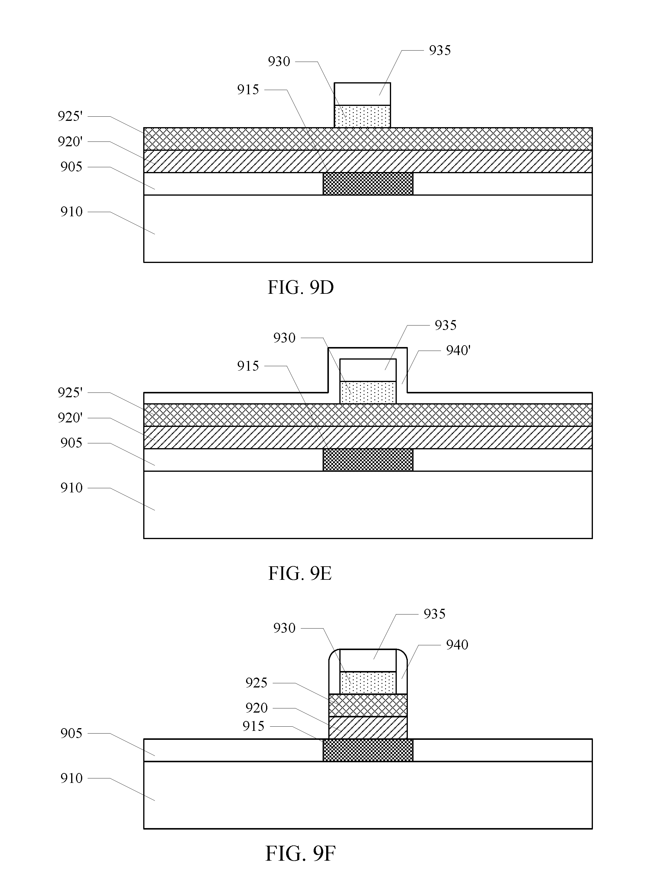
D00013
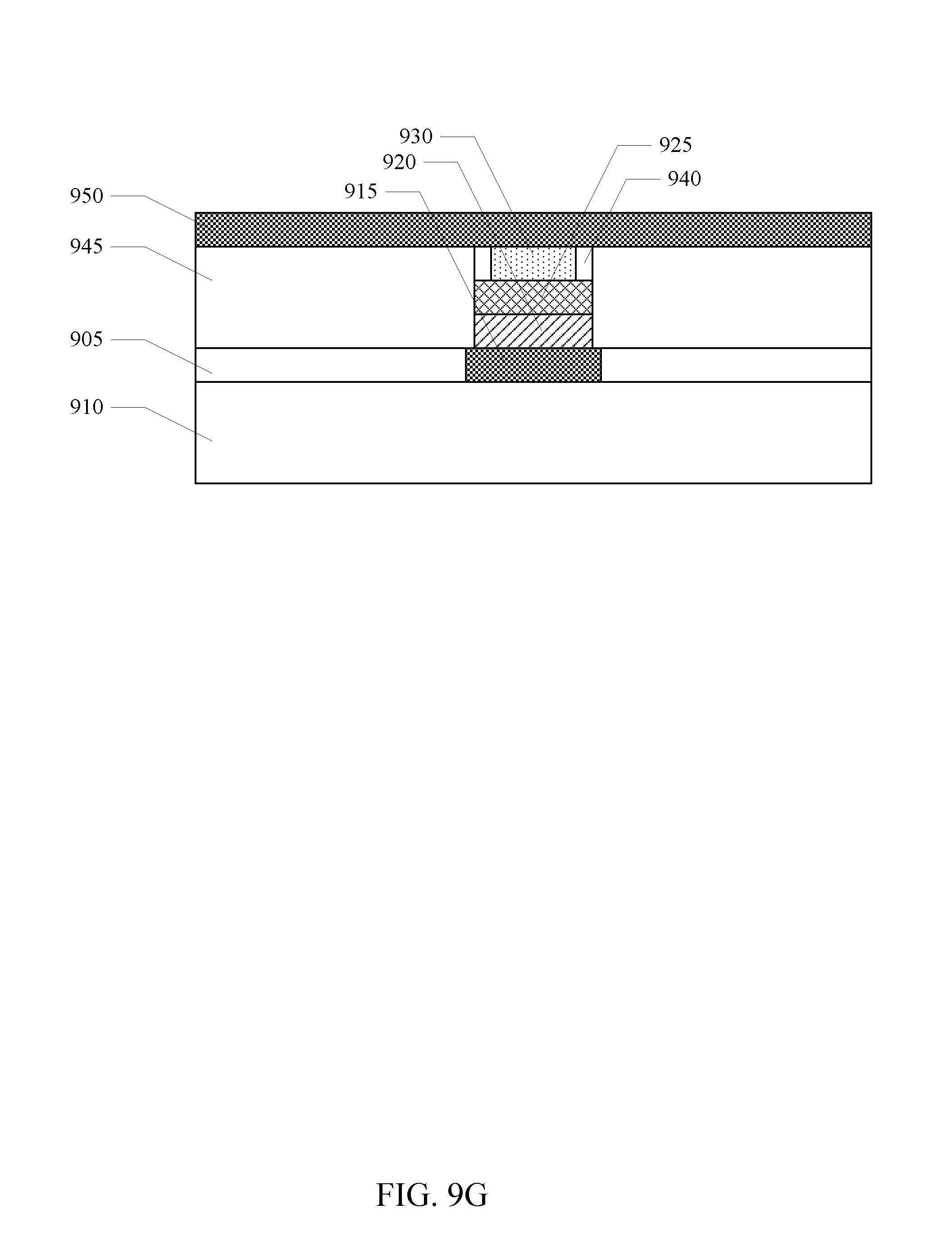
D00014
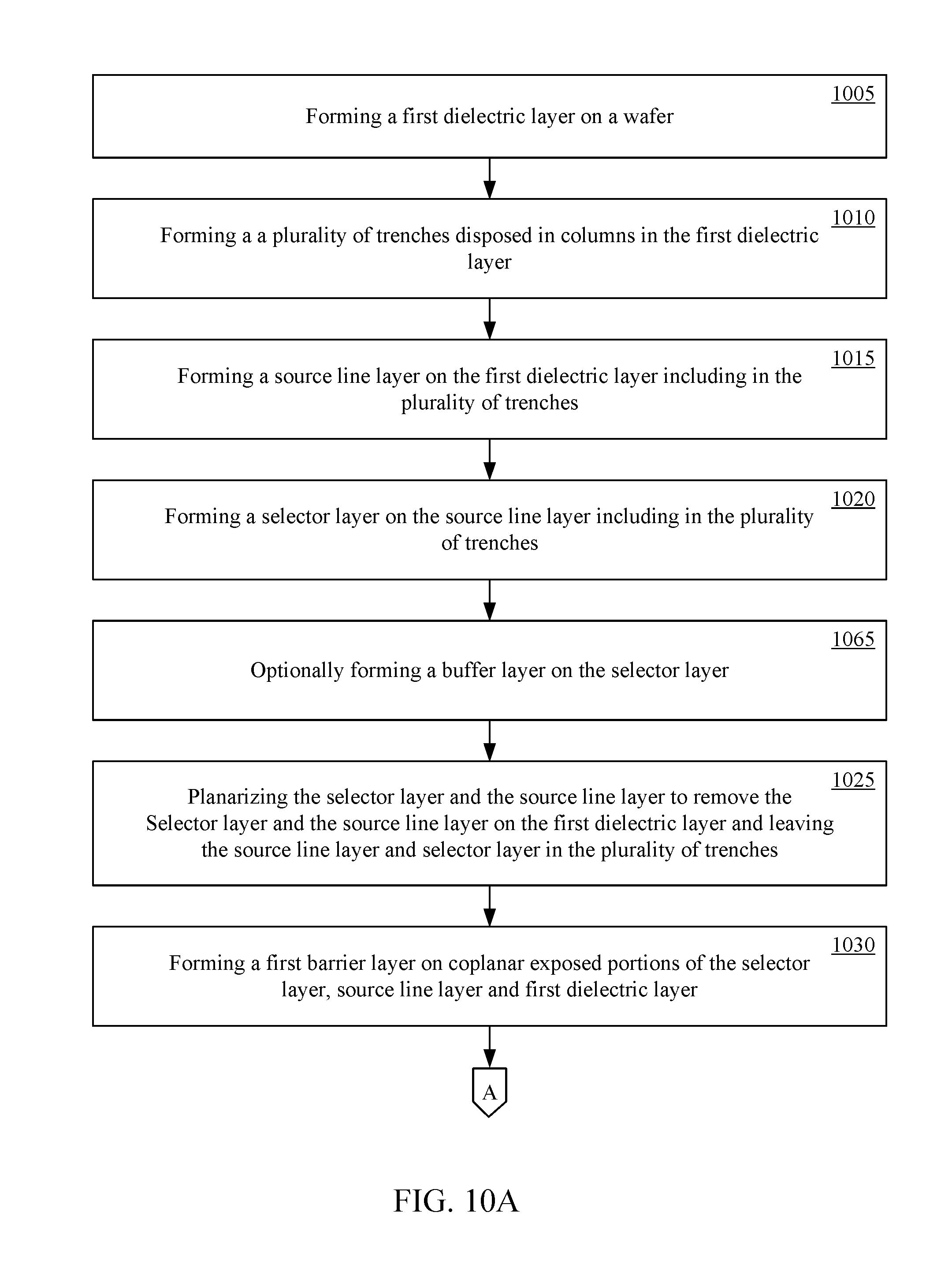
D00015
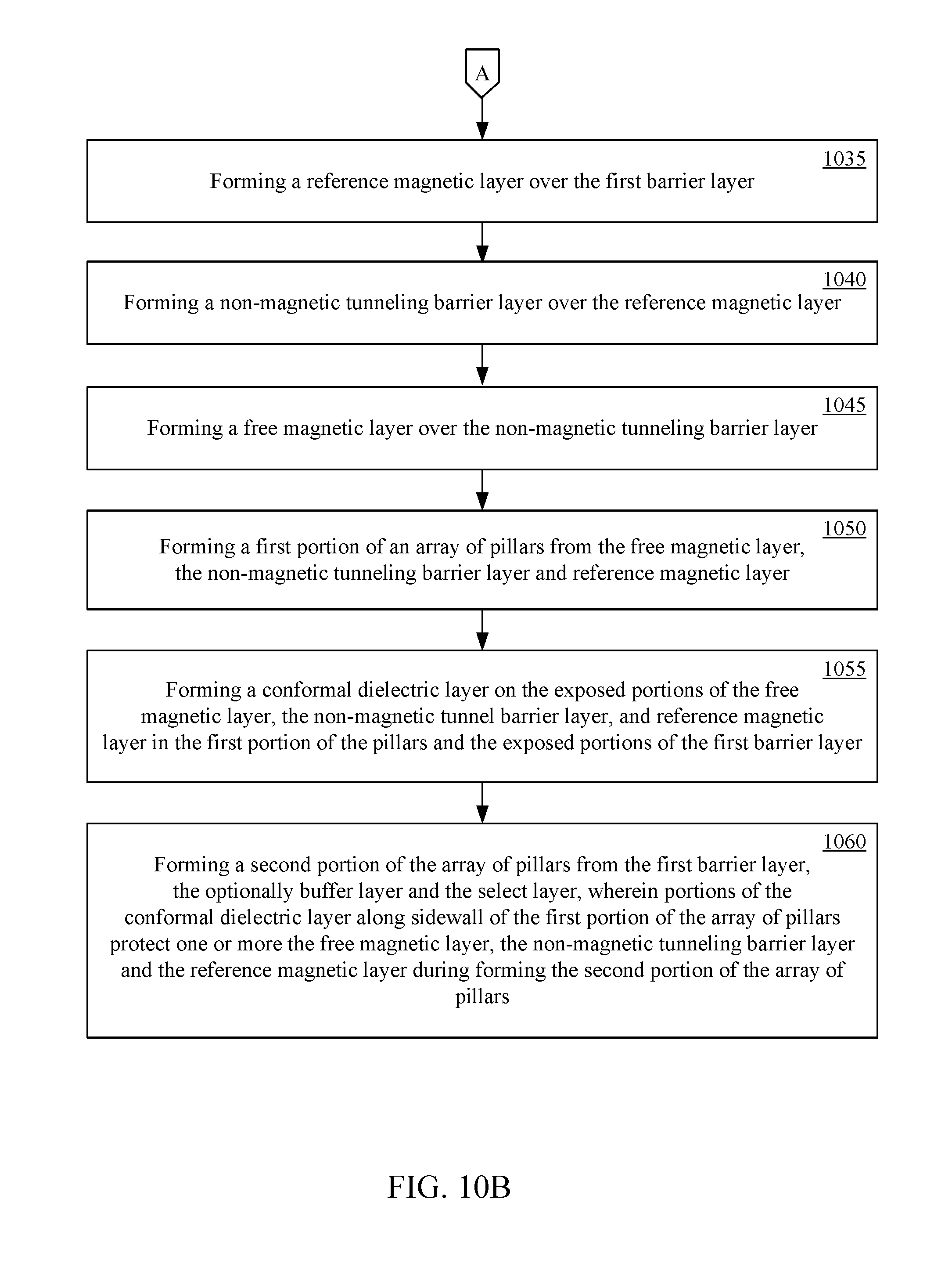
D00016
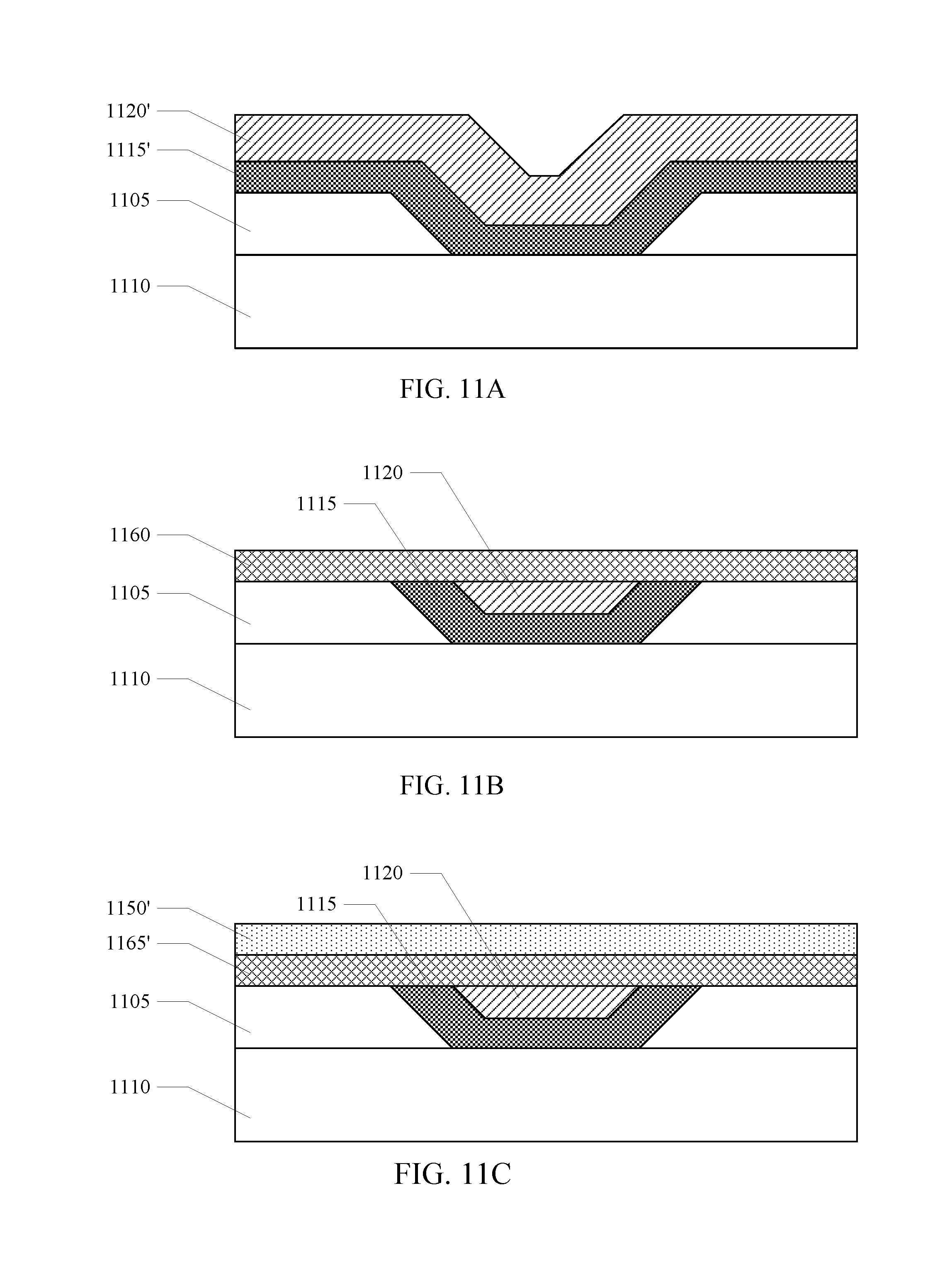
D00017
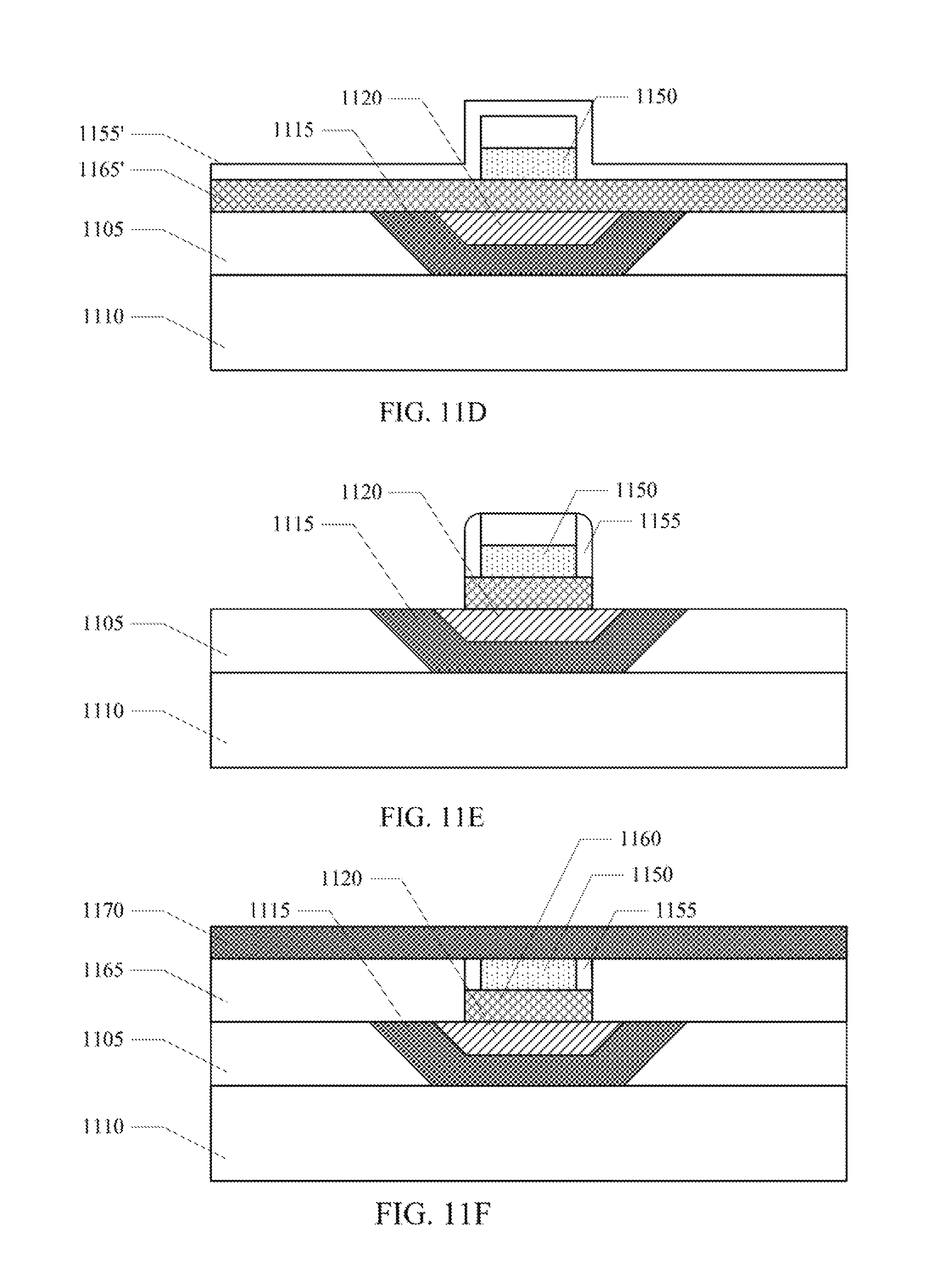
D00018
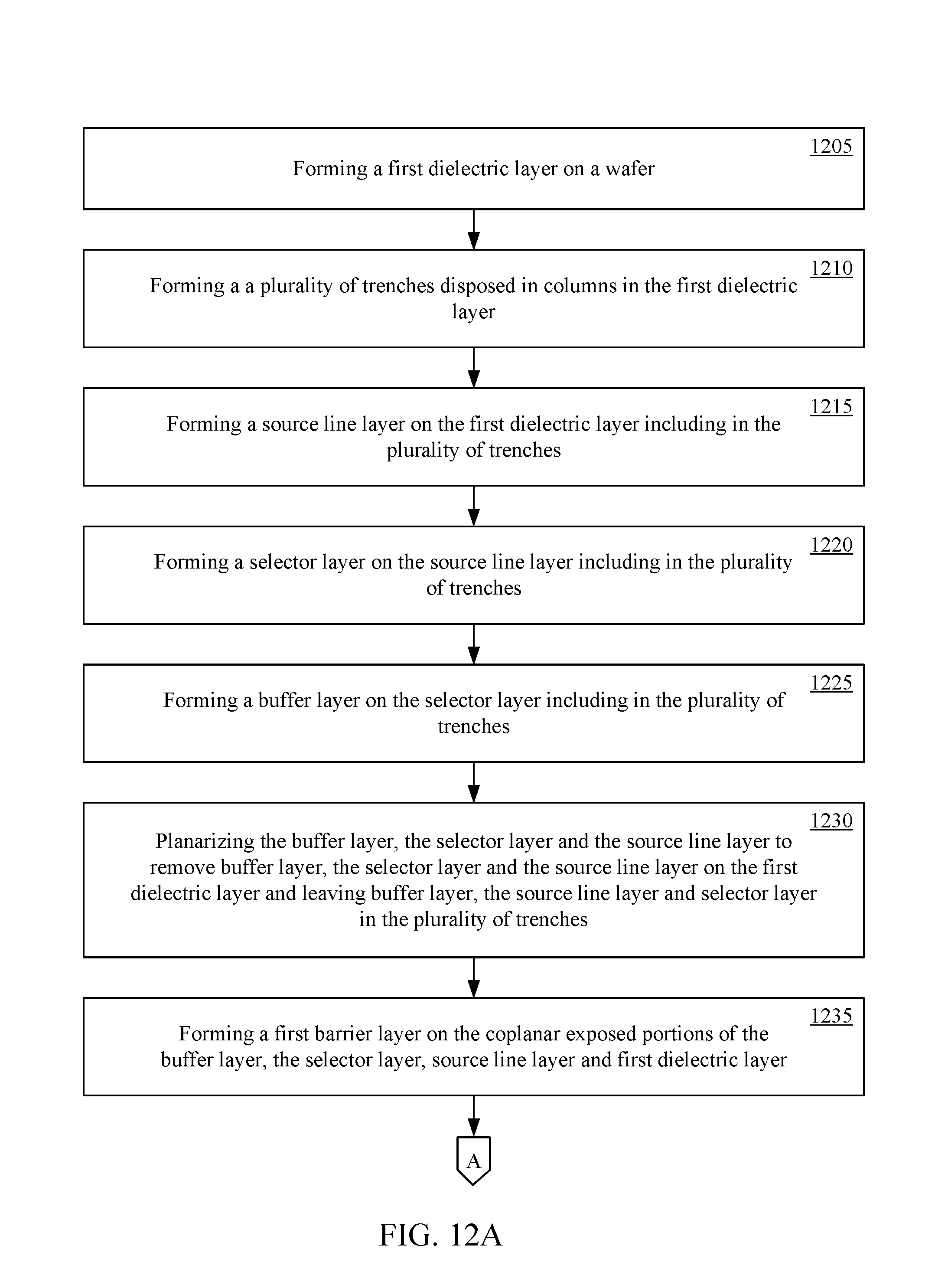
D00019
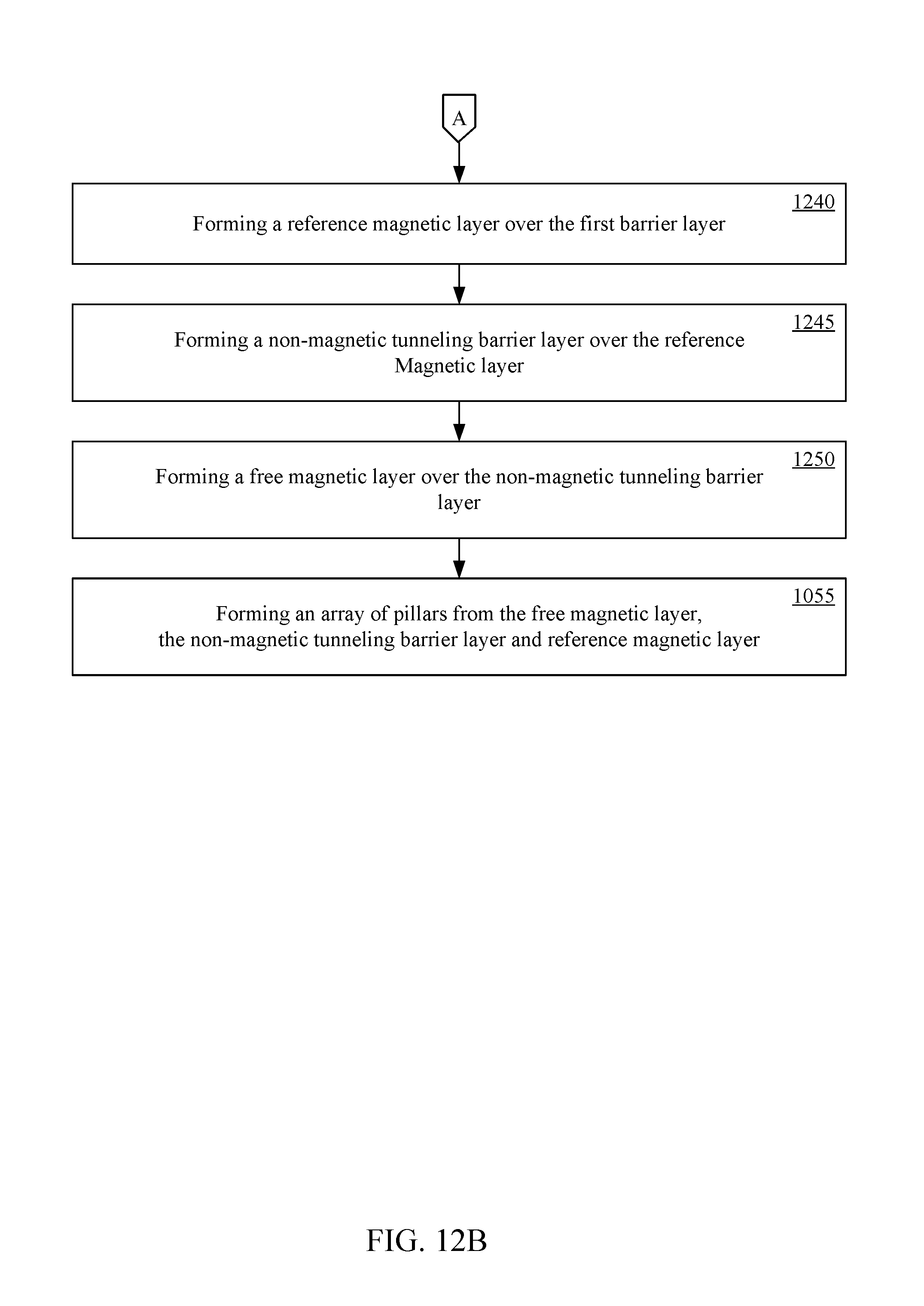
D00020
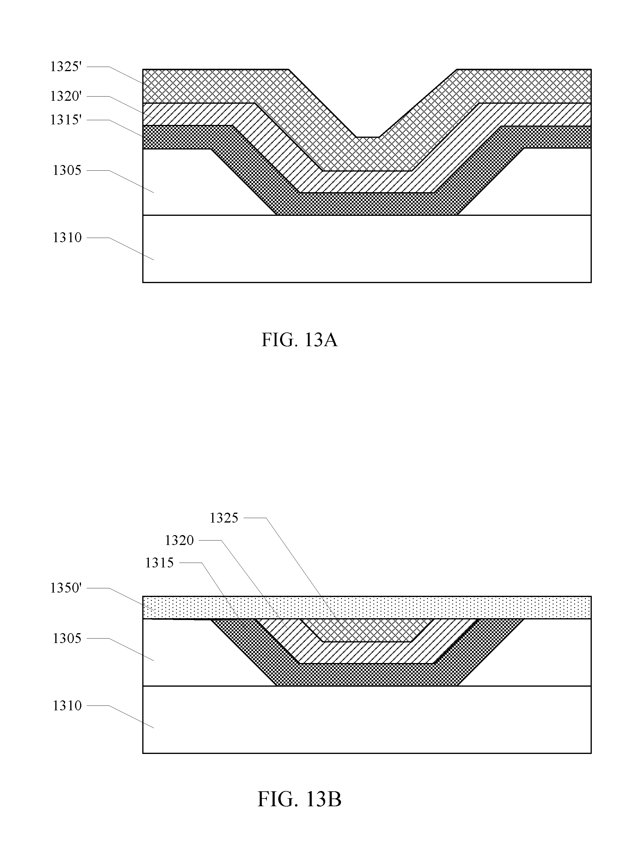
D00021
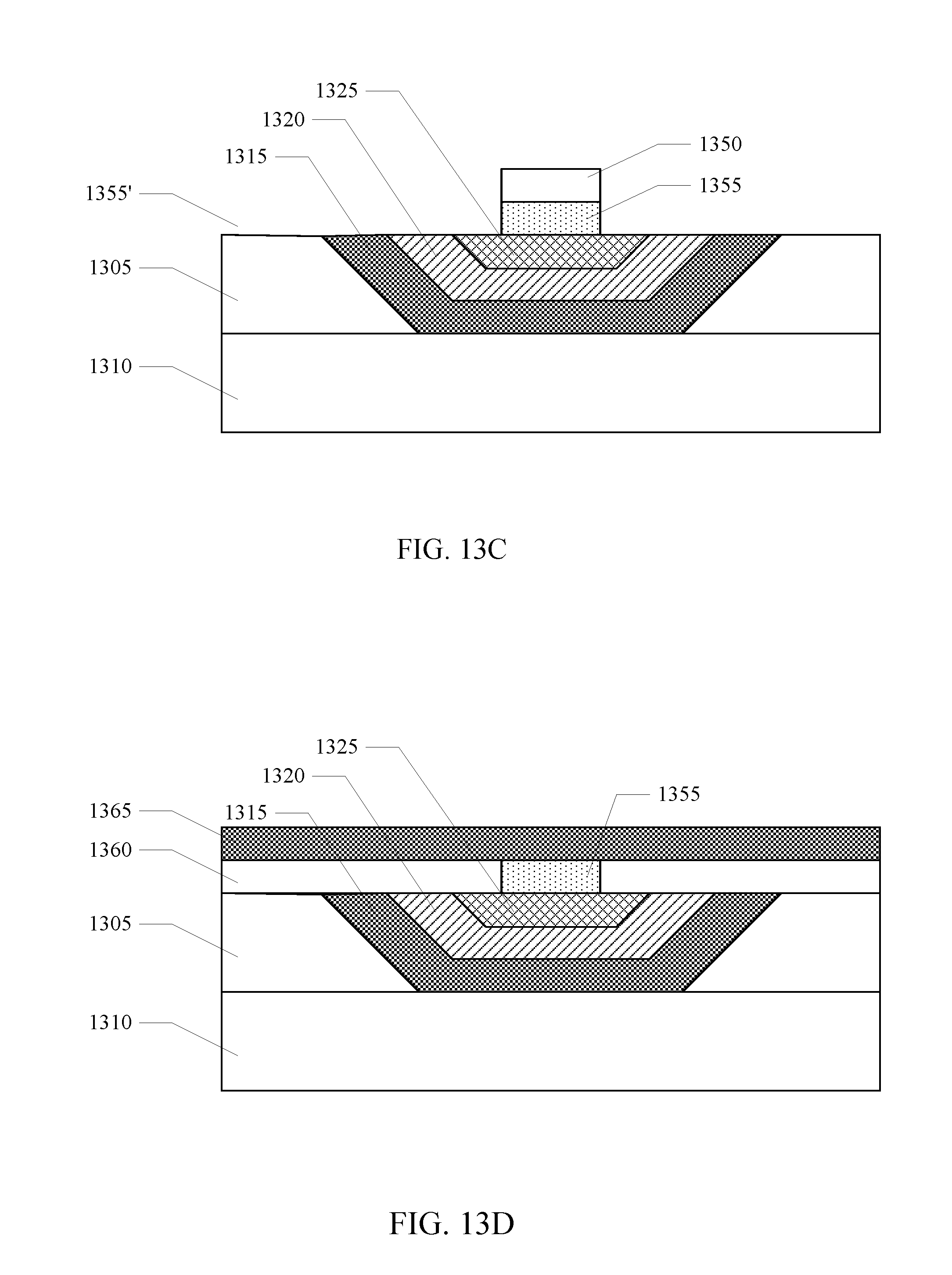
D00022

D00023
D00024
D00025
D00026
D00027
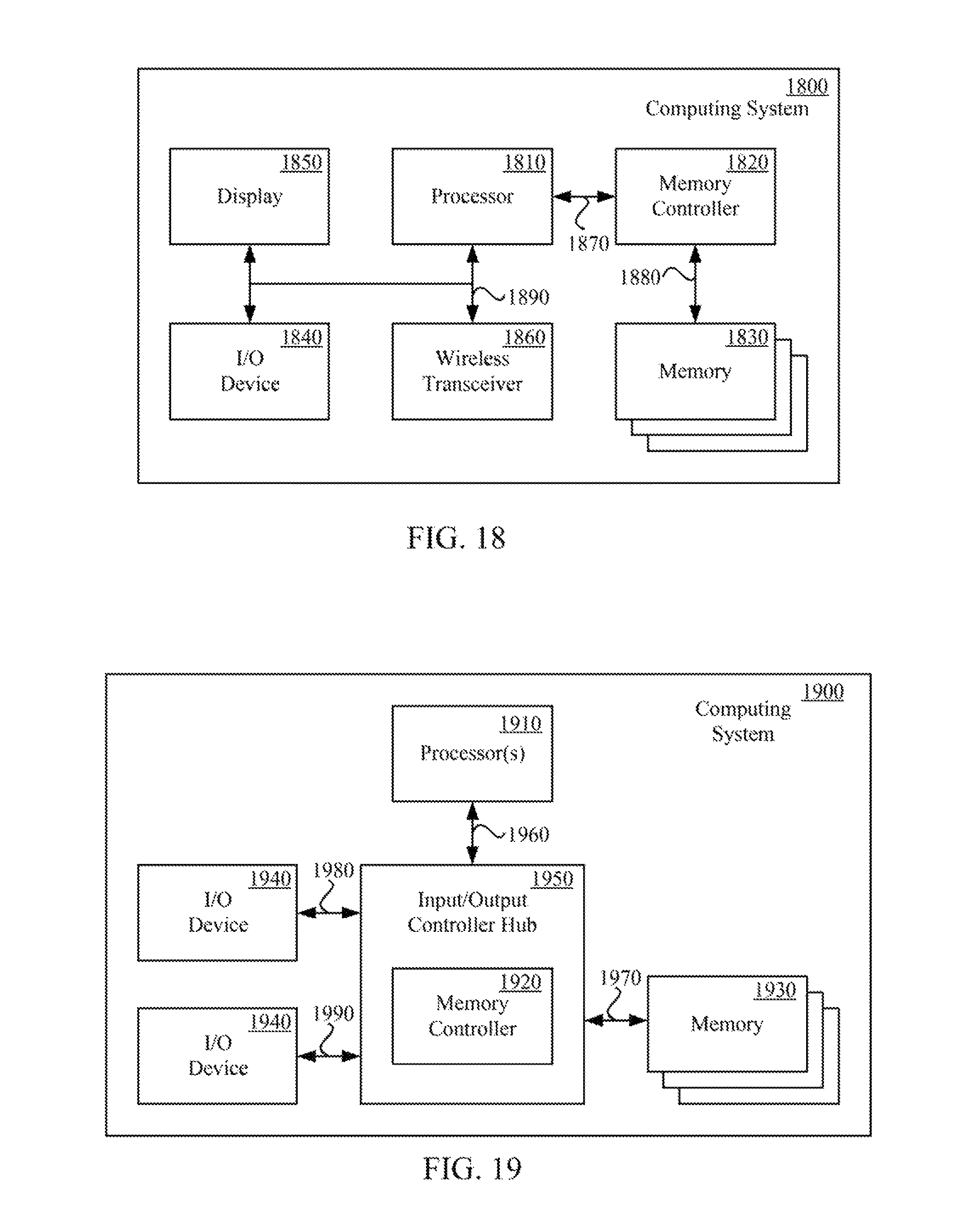
D00028
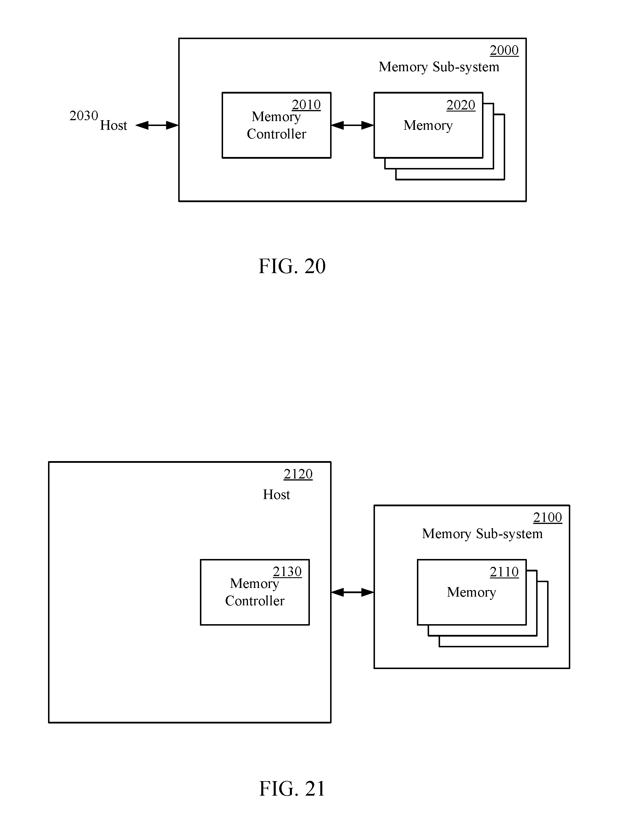
XML
uspto.report is an independent third-party trademark research tool that is not affiliated, endorsed, or sponsored by the United States Patent and Trademark Office (USPTO) or any other governmental organization. The information provided by uspto.report is based on publicly available data at the time of writing and is intended for informational purposes only.
While we strive to provide accurate and up-to-date information, we do not guarantee the accuracy, completeness, reliability, or suitability of the information displayed on this site. The use of this site is at your own risk. Any reliance you place on such information is therefore strictly at your own risk.
All official trademark data, including owner information, should be verified by visiting the official USPTO website at www.uspto.gov. This site is not intended to replace professional legal advice and should not be used as a substitute for consulting with a legal professional who is knowledgeable about trademark law.