System and method to measure capacitance of capacitive sensor array
Moyal , et al. A
U.S. patent number 10,386,969 [Application Number 13/670,671] was granted by the patent office on 2019-08-20 for system and method to measure capacitance of capacitive sensor array. This patent grant is currently assigned to Cypress Semiconductor Corporation. The grantee listed for this patent is Cypress Semiconductor Corporation. Invention is credited to Nathan Y. Moyal, Dana Jon Olson.


| United States Patent | 10,386,969 |
| Moyal , et al. | August 20, 2019 |
System and method to measure capacitance of capacitive sensor array
Abstract
A system and method for determining position information. The method includes selecting a column, a first row, and a second row of a capacitive sensor array. The first row and second row intersect with the column of the capacitive sensor array. The method further includes measuring a differential capacitance between the first row and the second row and utilizing the differential capacitance in determining a location of an object proximate to the capacitive sensor array.
| Inventors: | Moyal; Nathan Y. (West Linn, OR), Olson; Dana Jon (Kirkland, WA) | ||||||||||
|---|---|---|---|---|---|---|---|---|---|---|---|
| Applicant: |
|
||||||||||
| Assignee: | Cypress Semiconductor
Corporation (San Jose, CA) |
||||||||||
| Family ID: | 47190959 | ||||||||||
| Appl. No.: | 13/670,671 | ||||||||||
| Filed: | November 7, 2012 |
Related U.S. Patent Documents
| Application Number | Filing Date | Patent Number | Issue Date | ||
|---|---|---|---|---|---|
| 12239692 | Sep 26, 2008 | 8321174 | |||
| Current U.S. Class: | 1/1 |
| Current CPC Class: | G06F 3/0416 (20130101); G06F 3/044 (20130101) |
| Current International Class: | G01C 9/00 (20060101); G06F 3/044 (20060101) |
| Field of Search: | ;702/150 |
References Cited [Referenced By]
U.S. Patent Documents
| 3660801 | May 1972 | Paulfus |
| 3921167 | November 1975 | Fox |
| 3979745 | September 1976 | Bishop |
| 4039940 | August 1977 | Butler et al. |
| 4090092 | May 1978 | Serrano |
| 4103252 | July 1978 | Bobick |
| 4113378 | September 1978 | Wirtz |
| 4145748 | March 1979 | Eichelberger et al. |
| 4193063 | March 1980 | Hitt et al. |
| 4238711 | December 1980 | Wallot |
| 4264903 | April 1981 | Bigelow |
| 4266144 | May 1981 | Bristol |
| 4283713 | August 1981 | Philipp |
| 4292604 | September 1981 | Embree et al. |
| 4293734 | October 1981 | Pepper, Jr. |
| 4305135 | December 1981 | Dahl et al. |
| 4438404 | March 1984 | Philipp |
| 4475151 | October 1984 | Philipp |
| 4497575 | February 1985 | Philipp |
| 4558274 | December 1985 | Carusillo |
| 4560830 | December 1985 | Perl |
| 4586260 | May 1986 | Baxter et al. |
| 4614937 | September 1986 | Poujois |
| 4728932 | March 1988 | Atherton |
| 4736097 | April 1988 | Philipp |
| 4736191 | April 1988 | Matzke et al. |
| 4742331 | May 1988 | Barrow et al. |
| 4772983 | September 1988 | Kerber et al. |
| 4773024 | September 1988 | Faggin et al. |
| 4802103 | January 1989 | Faggin et al. |
| 4806709 | February 1989 | Evans |
| 4825147 | April 1989 | Cook et al. |
| 4831325 | May 1989 | Watson, Jr. |
| 4876534 | October 1989 | Mead et al. |
| 4878013 | October 1989 | Andermo |
| 4879461 | November 1989 | Philipp |
| 4879505 | November 1989 | Barrow et al. |
| 4879508 | November 1989 | Andermo |
| 4920399 | April 1990 | Hall |
| 4935702 | June 1990 | Mead et al. |
| 4940980 | July 1990 | Tice |
| 4953928 | September 1990 | Anderson et al. |
| 4962342 | October 1990 | Mead et al. |
| 4977480 | December 1990 | Nishihara |
| 5008497 | April 1991 | Asher |
| 5049758 | September 1991 | Mead et al. |
| 5055827 | October 1991 | Philipp |
| 5059920 | October 1991 | Anderson et al. |
| 5068622 | November 1991 | Mead et al. |
| 5073759 | December 1991 | Mead et al. |
| 5083044 | January 1992 | Mead et al. |
| 5089757 | February 1992 | Wilson |
| 5095284 | March 1992 | Mead |
| 5097305 | March 1992 | Mead et al. |
| 5107149 | April 1992 | Platt et al. |
| 5109261 | April 1992 | Mead et al. |
| 5119038 | June 1992 | Anderson et al. |
| 5120996 | June 1992 | Mead et al. |
| 5122800 | June 1992 | Philipp |
| 5126685 | June 1992 | Platt et al. |
| 5146106 | September 1992 | Anderson et al. |
| 5160899 | November 1992 | Anderson et al. |
| 5165054 | November 1992 | Platt et al. |
| 5166562 | November 1992 | Allen et al. |
| 5204549 | April 1993 | Platt et al. |
| 5214388 | May 1993 | Vranish et al. |
| 5237879 | August 1993 | Speeter |
| 5243554 | September 1993 | Allen et al. |
| 5248873 | September 1993 | Allen et al. |
| 5260592 | November 1993 | Mead et al. |
| 5270963 | December 1993 | Allen et al. |
| 5276407 | January 1994 | Mead et al. |
| 5281862 | January 1994 | Ma |
| 5289023 | February 1994 | Mead |
| 5294889 | March 1994 | Heep et al. |
| 5303329 | April 1994 | Mead et al. |
| 5305017 | April 1994 | Gerpheide |
| 5323158 | June 1994 | Ferguson, Jr. |
| 5324958 | June 1994 | Mead et al. |
| 5331215 | July 1994 | Allen et al. |
| 5336936 | August 1994 | Allen et al. |
| 5339213 | August 1994 | O'Callaghan |
| 5349303 | September 1994 | Gerpheide |
| 5373245 | December 1994 | Vranish et al. |
| 5374787 | December 1994 | Miller et al. |
| 5381515 | January 1995 | Platt et al. |
| 5384467 | January 1995 | Plimon et al. |
| 5386219 | January 1995 | Greanias et al. |
| 5408194 | April 1995 | Steinbach et al. |
| 5412387 | May 1995 | Vincelette et al. |
| 5424756 | June 1995 | Ho et al. |
| 5461321 | October 1995 | Sanders et al. |
| 5479103 | December 1995 | Kernahan et al. |
| 5488204 | January 1996 | Mead et al. |
| 5495077 | February 1996 | Miller et al. |
| 5518078 | May 1996 | Tsujioka et al. |
| 5525980 | June 1996 | Jahier et al. |
| 5541580 | July 1996 | Gerston et al. |
| 5541878 | July 1996 | Lemoncheck et al. |
| 5543588 | August 1996 | Bisset et al. |
| 5543590 | August 1996 | Gillespie et al. |
| 5543591 | August 1996 | Gillespie et al. |
| 5555907 | September 1996 | Philipp |
| 5565658 | October 1996 | Gerpheide et al. |
| 5566702 | October 1996 | Philipp |
| 5572205 | November 1996 | Caldwell et al. |
| 5589856 | December 1996 | Stein et al. |
| 5629891 | May 1997 | Lemoncheck et al. |
| 5648642 | July 1997 | Miller et al. |
| 5650597 | July 1997 | Redmayne |
| 5670915 | September 1997 | Cooper et al. |
| 5672959 | September 1997 | Der |
| 5680070 | October 1997 | Anderson et al. |
| 5682032 | October 1997 | Philipp |
| 5684487 | November 1997 | Timko |
| 5691513 | November 1997 | Yamamoto et al. |
| 5694063 | December 1997 | Burlison et al. |
| 5730165 | March 1998 | Philipp |
| 5748185 | May 1998 | Stephan et al. |
| 5757368 | May 1998 | Gerpheide et al. |
| 5760852 | June 1998 | Wu et al. |
| 5763909 | June 1998 | Mead et al. |
| 5763924 | June 1998 | Lum et al. |
| 5767457 | June 1998 | Gerpheide et al. |
| 5796183 | August 1998 | Hourmand et al. |
| 5801340 | September 1998 | Peter |
| 5812698 | September 1998 | Platt et al. |
| 5841078 | November 1998 | Miller et al. |
| 5844265 | December 1998 | Mead et al. |
| 5854625 | December 1998 | Frisch et al. |
| 5861583 | January 1999 | Schediwy et al. |
| 5861875 | January 1999 | Gerpheide |
| 5864242 | January 1999 | Allen et al. |
| 5864392 | January 1999 | Winklhofer et al. |
| 5880411 | March 1999 | Gillespie et al. |
| 5889236 | March 1999 | Gillespie et al. |
| 5905489 | May 1999 | Takahama et al. |
| 5914465 | June 1999 | Allen et al. |
| 5914708 | June 1999 | Lagrange et al. |
| 5920309 | July 1999 | Bisset et al. |
| 5920310 | July 1999 | Faggin et al. |
| 5926566 | July 1999 | Wang et al. |
| 5942733 | August 1999 | Allen et al. |
| 5943052 | August 1999 | Allen et al. |
| 5949264 | September 1999 | Lo |
| 5969513 | October 1999 | Clark |
| 6023422 | February 2000 | Allen et al. |
| 6028271 | February 2000 | Gillespie et al. |
| 6028959 | February 2000 | Wang et al. |
| 6037929 | March 2000 | Ogura et al. |
| 6037930 | March 2000 | Wolfe et al. |
| 6060957 | May 2000 | Kodrnja et al. |
| 6067019 | May 2000 | Scott |
| 6097432 | August 2000 | Mead et al. |
| 6140853 | October 2000 | Lo |
| 6145850 | November 2000 | Rehm |
| 6148104 | November 2000 | Wang et al. |
| 6184871 | February 2001 | Teres et al. |
| 6185450 | February 2001 | Seguine et al. |
| 6188228 | February 2001 | Philipp |
| 6188391 | February 2001 | Seely et al. |
| 6191723 | February 2001 | Lewis |
| 6222528 | April 2001 | Gerpheide et al. |
| 6239389 | May 2001 | Allen et al. |
| 6249447 | June 2001 | Boylan et al. |
| 6262717 | July 2001 | Donohue et al. |
| 6271719 | August 2001 | Sevastopoulos |
| 6271720 | August 2001 | Sevastopoulos |
| 6271835 | August 2001 | Hoeksma |
| 6278283 | August 2001 | Tsugai |
| 6280391 | August 2001 | Olson et al. |
| 6288707 | September 2001 | Philipp |
| 6295052 | September 2001 | Kato et al. |
| 6304014 | October 2001 | England et al. |
| 6320184 | November 2001 | Winklhofer et al. |
| 6323846 | November 2001 | Westerman et al. |
| 6326859 | December 2001 | Goldman et al. |
| 6342817 | January 2002 | Crofts et al. |
| 6344773 | February 2002 | Sevastopoulos et al. |
| 6353200 | March 2002 | Schwankhart |
| 6366099 | April 2002 | Reddi |
| 6377009 | April 2002 | Philipp |
| 6377129 | April 2002 | Rhee et al. |
| 6380929 | April 2002 | Platt |
| 6380931 | April 2002 | Gillespie et al. |
| 6400217 | June 2002 | Bhandari |
| 6414671 | July 2002 | Gillespie et al. |
| 6424338 | July 2002 | Anderson |
| 6430305 | August 2002 | Decker |
| 6441073 | August 2002 | Tanaka et al. |
| 6441682 | August 2002 | Vinn et al. |
| 6445257 | September 2002 | Cox et al. |
| 6448911 | September 2002 | Somayajula |
| 6452514 | September 2002 | Philipp |
| 6457355 | October 2002 | Philipp |
| 6459321 | October 2002 | Belch |
| 6466036 | October 2002 | Philipp |
| 6473069 | October 2002 | Gerpheide |
| 6476798 | November 2002 | Bertram et al. |
| 6489899 | December 2002 | Ely et al. |
| 6490203 | December 2002 | Tang |
| 6498720 | December 2002 | Glad |
| 6499359 | December 2002 | Washeleski et al. |
| 6522083 | February 2003 | Roach |
| 6522128 | February 2003 | Ely et al. |
| 6522187 | February 2003 | Sousa |
| 6523416 | February 2003 | Takagi et al. |
| 6529015 | March 2003 | Nonoyama et al. |
| 6534970 | March 2003 | Ely et al. |
| 6535200 | March 2003 | Philipp |
| 6570557 | May 2003 | Westerman et al. |
| 6574095 | June 2003 | Suzuki |
| 6577140 | June 2003 | Wenman |
| 6583632 | June 2003 | Von Basse et al. |
| 6587093 | July 2003 | Shaw et al. |
| 6597347 | July 2003 | Yasutake |
| 6610936 | August 2003 | Gillespie et al. |
| 6614313 | September 2003 | Crofts et al. |
| 6624640 | September 2003 | Lund et al. |
| 6639586 | October 2003 | Gerpheide |
| 6642857 | November 2003 | Schediwy et al. |
| 6649924 | November 2003 | Philipp et al. |
| 6667740 | December 2003 | Ely et al. |
| 6673308 | January 2004 | Hino et al. |
| 6677758 | January 2004 | Maki et al. |
| 6677932 | January 2004 | Westerman |
| 6680731 | January 2004 | Gerpheide et al. |
| 6683462 | January 2004 | Shimizu |
| 6690066 | February 2004 | Lin et al. |
| 6704005 | March 2004 | Kato et al. |
| 6705511 | March 2004 | Dames et al. |
| 6714817 | March 2004 | Daynes et al. |
| 6720777 | April 2004 | Wang |
| 6730863 | May 2004 | Gerpheide et al. |
| 6731121 | May 2004 | Hsu et al. |
| 6744258 | June 2004 | Ishio et al. |
| 6750852 | June 2004 | Gillespie et al. |
| 6768420 | July 2004 | McCarthy et al. |
| 6774644 | August 2004 | Eberlein |
| 6781577 | August 2004 | Shigetaka |
| 6788221 | September 2004 | Ely et al. |
| 6788521 | September 2004 | Nishi |
| 6798218 | September 2004 | Kasperkovitz |
| 6806693 | October 2004 | Bron |
| 6809275 | October 2004 | Cheng et al. |
| 6810442 | October 2004 | Lin et al. |
| 6825673 | November 2004 | Yamaoka |
| 6825890 | November 2004 | Matsufusa |
| 6829727 | December 2004 | Pawloski |
| 6838887 | January 2005 | Denen et al. |
| 6839052 | January 2005 | Kramer |
| 6856433 | February 2005 | Hatano et al. |
| 6859159 | February 2005 | Michalski |
| 6861961 | March 2005 | Sandbach et al. |
| 6873203 | March 2005 | Latham, II et al. |
| 6879215 | April 2005 | Roach |
| 6882338 | April 2005 | Flowers |
| 6888536 | May 2005 | Westerman et al. |
| 6888538 | May 2005 | Ely et al. |
| 6891531 | May 2005 | Lin |
| 6893724 | May 2005 | Lin et al. |
| 6897673 | May 2005 | Savage et al. |
| 6903402 | June 2005 | Miyazawa |
| 6904570 | June 2005 | Foote et al. |
| 6914547 | July 2005 | Swaroop et al. |
| 6933873 | August 2005 | Horsley et al. |
| 6940291 | September 2005 | Ozick |
| 6946853 | September 2005 | Gifford et al. |
| 6949811 | September 2005 | Miyazawa |
| 6949937 | September 2005 | Knoedgen |
| 6958594 | October 2005 | Redl et al. |
| 6969978 | November 2005 | Dening |
| 6970120 | November 2005 | Bjornsen |
| 6970126 | November 2005 | O'Dowd et al. |
| 6975123 | December 2005 | Malang et al. |
| 6993607 | January 2006 | Philipp |
| 6999009 | February 2006 | Monney |
| 7002557 | February 2006 | Iizuka et al. |
| 7006078 | February 2006 | Kim |
| 7006938 | February 2006 | Laraia et al. |
| 7030782 | April 2006 | Ely et al. |
| 7030860 | April 2006 | Hsu et al. |
| 7031886 | April 2006 | Hargreaves |
| 7032051 | April 2006 | Reay et al. |
| 7036096 | April 2006 | Sarkar et al. |
| 7046230 | May 2006 | Zadesky et al. |
| 7068039 | June 2006 | Parker |
| 7075316 | July 2006 | Umeda et al. |
| 7075523 | July 2006 | Marten et al. |
| 7075864 | July 2006 | Kakitsuka et al. |
| 7078916 | July 2006 | Denison |
| 7098675 | August 2006 | Inaba et al. |
| 7109978 | September 2006 | Gillespie et al. |
| 7119550 | October 2006 | Kitano et al. |
| 7129714 | October 2006 | Baxter |
| 7129935 | October 2006 | Mackey |
| 7133140 | November 2006 | Lukacs et al. |
| 7133793 | November 2006 | Ely et al. |
| 7136051 | November 2006 | Hein et al. |
| 7141968 | November 2006 | Hibbs et al. |
| 7141987 | November 2006 | Hibbs et al. |
| 7148704 | December 2006 | Philipp |
| 7151276 | December 2006 | Gerlach et al. |
| 7151528 | December 2006 | Taylor et al. |
| 7158056 | January 2007 | Wright et al. |
| 7158125 | January 2007 | Sinclair et al. |
| 7202655 | April 2007 | Itoh |
| 7202857 | April 2007 | Hinckley et al. |
| 7205777 | April 2007 | Schulz et al. |
| 7212189 | May 2007 | Shaw et al |
| 7224591 | May 2007 | Kaishita et al. |
| 7225090 | May 2007 | Coley |
| 7233508 | June 2007 | Itoh |
| 7235983 | June 2007 | O'Dowd et al. |
| 7245131 | July 2007 | Kurachi et al. |
| 7253643 | August 2007 | Seguine |
| 7254775 | August 2007 | Geaghan et al. |
| 7256588 | August 2007 | Howard et al. |
| 7262609 | August 2007 | Reynolds |
| 7271608 | September 2007 | Vermeire et al. |
| 7288946 | October 2007 | Hargreaves et al. |
| 7288977 | October 2007 | Stanley |
| 7298124 | November 2007 | Kan et al. |
| 7301350 | November 2007 | Hargreaves et al. |
| 7307485 | December 2007 | Snyder et al. |
| 7312616 | December 2007 | Snyder |
| 7323879 | January 2008 | Kuo et al. |
| 7323886 | January 2008 | Lee |
| 7333090 | February 2008 | Tanaka et al. |
| 7339580 | March 2008 | Westerman et al. |
| 7359816 | April 2008 | Kumar et al. |
| 7375535 | May 2008 | Kutz et al. |
| 7381031 | June 2008 | Kawaguchi et al. |
| 7392431 | June 2008 | Swoboda |
| 7417411 | August 2008 | Hoffman et al. |
| 7417441 | August 2008 | Reynolds |
| 7423437 | September 2008 | Hargreaves et al. |
| 7439962 | October 2008 | Reynolds et al. |
| 7449895 | November 2008 | Ely et al. |
| 7450113 | November 2008 | Gillespie et al. |
| 7451050 | November 2008 | Hargreaves |
| 7453270 | November 2008 | Hargreaves et al. |
| 7453279 | November 2008 | Corbin, Jr. et al. |
| 7466307 | December 2008 | Trent, Jr. et al. |
| 7479788 | January 2009 | Bolender et al. |
| 7495659 | February 2009 | Marriott et al. |
| 7499040 | March 2009 | Zadesky et al. |
| 7504833 | March 2009 | Seguine |
| 7515140 | April 2009 | Philipp |
| 7521941 | April 2009 | Ely et al. |
| RE40867 | August 2009 | Binstead |
| 7598752 | October 2009 | Li |
| 7598822 | October 2009 | Rajagopal et al. |
| 7656168 | February 2010 | Mahowald et al. |
| 7663607 | February 2010 | Hotelling et al. |
| 7667468 | February 2010 | Anderson |
| 7683641 | March 2010 | Hargreaves et al. |
| 7804307 | September 2010 | Bokma et al. |
| 7812827 | October 2010 | Hotelling et al. |
| 7812829 | October 2010 | Gillespie et al. |
| 7821274 | October 2010 | Philipp et al. |
| 7831070 | November 2010 | Cheng et al. |
| 7880481 | February 2011 | Zangl et al. |
| 7911456 | March 2011 | Gillespie et al. |
| 7932897 | April 2011 | Elias et al. |
| 7952366 | May 2011 | Philipp et al. |
| 7969166 | June 2011 | Fasshauer |
| 8040142 | October 2011 | Bokma et al. |
| 8040321 | October 2011 | Peng et al. |
| 8054299 | November 2011 | Krah |
| 8067948 | November 2011 | Sequine |
| 8068097 | November 2011 | Guanghai |
| 8072429 | December 2011 | Grivna |
| 8082566 | December 2011 | Stallings |
| 8089288 | January 2012 | Maharita |
| 8089289 | January 2012 | Kremin et al. |
| 8093914 | January 2012 | Maharyta et al. |
| 8094128 | January 2012 | Vu et al. |
| 8144125 | March 2012 | Peng et al. |
| 8144126 | March 2012 | Wright |
| 8169238 | May 2012 | Maharyta et al. |
| 8358142 | January 2013 | Maharyta |
| 8525798 | September 2013 | Peterson et al. |
| 2001/0012667 | August 2001 | Ma et al. |
| 2002/0000978 | January 2002 | Gerpheide |
| 2002/0063688 | May 2002 | Shaw et al. |
| 2002/0067348 | June 2002 | Masters et al. |
| 2002/0080014 | June 2002 | Mccarthy et al. |
| 2002/0109035 | August 2002 | Denen et al. |
| 2002/0136372 | September 2002 | Bozorgui-Nesbat |
| 2002/0140440 | October 2002 | Haase |
| 2002/0191029 | December 2002 | Gillespie et al. |
| 2003/0014239 | January 2003 | Ichbiah et al. |
| 2003/0025679 | February 2003 | Taylor et al. |
| 2003/0062889 | April 2003 | Ely et al. |
| 2003/0063073 | April 2003 | Geaghan et al. |
| 2003/0063428 | April 2003 | Nishi |
| 2003/0076306 | April 2003 | Zadesky et al. |
| 2003/0080755 | May 2003 | Kobayashi |
| 2003/0091220 | May 2003 | Sato et al. |
| 2003/0098858 | May 2003 | Perski et al. |
| 2003/0112021 | June 2003 | Palata et al. |
| 2003/0156098 | August 2003 | Shaw et al. |
| 2003/0160808 | August 2003 | Foote et al. |
| 2003/0178675 | September 2003 | Nishizaka et al. |
| 2003/0183864 | October 2003 | Miyazawa |
| 2003/0183884 | October 2003 | Miyazawa |
| 2003/0184315 | October 2003 | Eberlein |
| 2003/0189419 | October 2003 | Maki et al. |
| 2003/0230438 | December 2003 | Keefer et al. |
| 2003/0232507 | December 2003 | Chen |
| 2004/0041798 | March 2004 | Kim |
| 2004/0056845 | March 2004 | Harkcom et al. |
| 2004/0068409 | April 2004 | Tanaka et al. |
| 2004/0082198 | April 2004 | Nakamura et al. |
| 2004/0169594 | September 2004 | Ely et al. |
| 2004/0178989 | September 2004 | Shahoian et al. |
| 2004/0178997 | September 2004 | Gillespie et al. |
| 2004/0183560 | September 2004 | Savage et al. |
| 2004/0217945 | November 2004 | Miyamoto et al. |
| 2004/0239616 | December 2004 | Collins |
| 2004/0239650 | December 2004 | Mackey |
| 2004/0252109 | December 2004 | Trent et al. |
| 2004/0263864 | December 2004 | Lukacs et al. |
| 2005/0021269 | January 2005 | Ely et al. |
| 2005/0024341 | February 2005 | Gillespie et al. |
| 2005/0031175 | February 2005 | Hara et al. |
| 2005/0062732 | March 2005 | Sinclair et al. |
| 2005/0073302 | April 2005 | Hibbs et al. |
| 2005/0073322 | April 2005 | Hibbs et al. |
| 2005/0083110 | April 2005 | Latham, II et al. |
| 2005/0099188 | May 2005 | Baxter |
| 2005/0159126 | July 2005 | Wang |
| 2005/0169768 | August 2005 | Kawaguchi et al. |
| 2005/0179668 | August 2005 | Edwards |
| 2005/0270273 | December 2005 | Marten |
| 2005/0275382 | December 2005 | Stessman et al. |
| 2005/0280639 | December 2005 | Taylor et al. |
| 2005/0283330 | December 2005 | Laraia et al. |
| 2006/0022660 | February 2006 | Itoh |
| 2006/0026535 | February 2006 | Hotelling et al. |
| 2006/0032680 | February 2006 | Elias et al. |
| 2006/0033508 | February 2006 | Lee |
| 2006/0033724 | February 2006 | Chaudhri et al. |
| 2006/0038793 | February 2006 | Philipp |
| 2006/0049834 | March 2006 | Umeda |
| 2006/0053387 | March 2006 | Ording |
| 2006/0066582 | March 2006 | Lyon et al. |
| 2006/0066585 | March 2006 | Lin |
| 2006/0097991 | May 2006 | Hotelling |
| 2006/0097992 | May 2006 | Gitzinger et al. |
| 2006/0108349 | May 2006 | Finley et al. |
| 2006/0113974 | June 2006 | Kan et al. |
| 2006/0114247 | June 2006 | Brown |
| 2006/0139469 | June 2006 | Yokota et al. |
| 2006/0152739 | July 2006 | Silvestre |
| 2006/0164142 | July 2006 | Stanley |
| 2006/0172767 | August 2006 | Cathey et al. |
| 2006/0176718 | August 2006 | Itoh |
| 2006/0187214 | August 2006 | Gillespie et al. |
| 2006/0193156 | August 2006 | Kaishita et al. |
| 2006/0197750 | September 2006 | Kerr et al. |
| 2006/0197752 | September 2006 | Hurst et al. |
| 2006/0221061 | October 2006 | Fry |
| 2006/0227117 | October 2006 | Proctor |
| 2006/0232559 | October 2006 | Chien et al. |
| 2006/0256090 | November 2006 | Huppi |
| 2006/0258390 | November 2006 | Cui et al. |
| 2006/0262101 | November 2006 | Layton et al. |
| 2006/0267953 | November 2006 | Peterson et al. |
| 2006/0273804 | December 2006 | Delorme et al. |
| 2006/0290678 | December 2006 | Lii |
| 2007/0046299 | March 2007 | Hargreaves et al. |
| 2007/0069274 | March 2007 | Elsass et al. |
| 2007/0074913 | April 2007 | Geaghan et al. |
| 2007/0076897 | April 2007 | Philipp |
| 2007/0100566 | May 2007 | Coley |
| 2007/0132737 | June 2007 | Mulligan et al. |
| 2007/0152983 | July 2007 | Mckillop et al. |
| 2007/0164756 | July 2007 | Lee |
| 2007/0173220 | July 2007 | Kim et al. |
| 2007/0176609 | August 2007 | Ely et al. |
| 2007/0176903 | August 2007 | Dahlin et al. |
| 2007/0228256 | October 2007 | Mentzer et al. |
| 2007/0229469 | October 2007 | Seguine |
| 2007/0236478 | October 2007 | Geaghan et al. |
| 2007/0257894 | November 2007 | Philipp |
| 2007/0263191 | November 2007 | Shibazaki |
| 2007/0268243 | November 2007 | Choo et al. |
| 2007/0268265 | November 2007 | Xiaoping |
| 2007/0268273 | November 2007 | Westerman et al. |
| 2007/0268274 | November 2007 | Westerman et al. |
| 2007/0268275 | November 2007 | Westerman et al. |
| 2007/0273659 | November 2007 | Xiaoping et al. |
| 2007/0291013 | December 2007 | Won |
| 2007/0296709 | December 2007 | Guanghai |
| 2008/0007529 | January 2008 | Paun et al. |
| 2008/0007534 | January 2008 | Peng et al. |
| 2008/0024455 | January 2008 | Lee et al. |
| 2008/0036473 | February 2008 | Jansson |
| 2008/0041639 | February 2008 | Westerman et al. |
| 2008/0041640 | February 2008 | Gillespie et al. |
| 2008/0042986 | February 2008 | Westerman et al. |
| 2008/0042987 | February 2008 | Westerman et al. |
| 2008/0042988 | February 2008 | Westerman et al. |
| 2008/0042989 | February 2008 | Westerman et al. |
| 2008/0042994 | February 2008 | Gillespie et al. |
| 2008/0047764 | February 2008 | Lee |
| 2008/0048997 | February 2008 | Gillespie et al. |
| 2008/0062139 | March 2008 | Hotelling et al. |
| 2008/0062140 | March 2008 | Hotelling et al. |
| 2008/0062148 | March 2008 | Hotelling et al. |
| 2008/0068100 | March 2008 | Goodnow et al. |
| 2008/0072192 | March 2008 | Lenahan |
| 2008/0088595 | April 2008 | Liu et al. |
| 2008/0111714 | May 2008 | Kremin |
| 2008/0116904 | May 2008 | Reynolds et al. |
| 2008/0128182 | June 2008 | Westerman et al. |
| 2008/0150906 | June 2008 | Grivna |
| 2008/0158177 | July 2008 | Wilson et al. |
| 2008/0158178 | July 2008 | Hotelling et al. |
| 2008/0162997 | July 2008 | Vu et al. |
| 2008/0165134 | July 2008 | Krah |
| 2008/0179112 | July 2008 | Qin et al. |
| 2008/0180399 | July 2008 | Cheng |
| 2008/0196945 | August 2008 | Konstas |
| 2008/0250864 | October 2008 | Shipton |
| 2008/0266263 | October 2008 | Motaparti et al. |
| 2008/0278178 | November 2008 | Philipp |
| 2008/0309623 | December 2008 | Hotelling et al. |
| 2008/0309634 | December 2008 | Hotelling et al. |
| 2009/0002206 | January 2009 | Kremin |
| 2009/0096758 | April 2009 | Hotelling et al. |
| 2009/0153152 | June 2009 | Maharyta et al. |
| 2009/0322351 | December 2009 | Mcleod |
| 2010/0001973 | January 2010 | Hotelling et al. |
| 2010/0328262 | December 2010 | Huang et al. |
| 2011/0025629 | February 2011 | Grivna et al. |
| 2011/0234523 | September 2011 | Chang et al. |
| 2012/0043140 | February 2012 | Peterson et al. |
| 2012/0043973 | February 2012 | Kremin |
| 2013/0049771 | February 2013 | Peng et al. |
| 2013/0127779 | May 2013 | Lillie et al. |
| 0574213 | Dec 1993 | EP | |||
| 05000604 | Feb 2005 | GB | |||
| 04012528 | Jan 1992 | JP | |||
| 05283519 | Oct 1993 | JP | |||
| 6104334 | Apr 1994 | JP | |||
| 6163528 | Jun 1994 | JP | |||
| 0002188 | Jan 2000 | WO | |||
Other References
|
Janusz Mlodzianowski, "A Simple Multipurpose Logic Analyzer," Dec. 1997, Circuit Cellar Ink. Issue 89, pp. 28-36. cited by applicant . Kremin, V. "Noise resistant capacitive sensor," U.S. Appl. No. 11/8244,249, filed Jun. 29, 2007: 41 pages. cited by applicant . Larry K. Baxter "Capacitive Sensors, Design and Applications" IEEE Press, The Institute of Electrical and Electronics Engineers Inc., Aug. 1996. pp. 177-187; 12 pages. cited by applicant . Lee, Mark; "EMC Design Considerations for PSoC CapSense Applications," Cypress Semiconductor Corporation, Application Note AN2318: Sep. 16, 2005, 6 pages. cited by applicant . Mark Lee, "CapSense Best Practices," Cypress Semiconductor Application Note. Oct. 16, 2006; 10 pages. cited by applicant . Milton Ohring, "The Materials Science of Thin Films: Deposition and Structure," 2nd Edition, Academic Press, 2002, pp. 336-337; 4 pages. cited by applicant . Min et al., "Offset Compensaton of Capacitive Sensors for Electrostatic Microactuators." ISIE 2001, Pusan Korea, pp. 2114-2117. cited by applicant . Ryan Seguine et al, "Layout Guidelines for PSoC CapSense", Cypress Application Note AN2292, Revision B, Oct. 31, 2005, all pages. cited by applicant . Sangil Park, "Motorola Digital Signal Processors, Principles of Sigma-Delta Modulation for Analog-to-Digital Converters," Rev. 1, downloaded from <http://digitalsignallabs.com/SigmaDelta.pdf>, Mar. 1997; 64 pages. cited by applicant . Sedra, Adel S. et al., "Microelectronic Circuits," 3rd Edition, Oxford University Press, pp. xiii-xx and 861-883, 1991; 20 pages. cited by applicant . Seguine, Ryan "Layout Guidelines for PSoC CapSense," Cypress Semiconductor Corporation, Application Note AN2292; Jul. 22, 2005, 13 pages. cited by applicant . SIPO 1st Office Action for Application No. 200880120802.9 dated Nov. 5, 2012: 6 pages. cited by applicant . Ted Tsui, "Migrating from CSR to CSD," Cypress Semiconductor Corporation, Application Note AN2408, Feb. 8, 2007, http://www.cypress.com. cited by applicant . The Authoritative Dictionary of IEEE Standards Terms, 2000, IEEE Press Publications, 7th Edition, pp. 1133-1134; 4 pages. cited by applicant . The Written Opinion of the International Searching Authority for International Application No. PCT/US05/23468 dated Aug. 25, 2006; 7 pages. cited by applicant . USPTO Advisory Action for U.S. Appl. No. 11/230,719 dated Nov. 30, 2007; 3 pages. cited by applicant . USPTO Advisory Action for U.S. Appl. No. 11/337,272 dated Apr. 3, 2007; 3 pages. cited by applicant . USPTO Advisory Action for U.S. Appl. No. 11/395,417 dated Jul. 6, 2007; 3 pages. cited by applicant . USPTO Advisory Action for U.S. Appl. No. 11/437,517 dated Apr. 7, 2010; 3 pages. cited by applicant . USPTO Advisory Action for U.S. Appl. No. 11/442,212 dated Jan. 5, 2011; 3 pages. cited by applicant . USPTO Advisory Action for U.S. Appl. No. 11/442,212 dated Dec. 17, 2009; 3 pages. cited by applicant . USPTO Advisory Action for U.S. Appl. No. 11/477,179 dated Jun. 7, 2010; 3 pages. cited by applicant . USPTO Advisory Action for U.S. Appl. No. 11/512,042 dated Feb. 23, 2011; 3 pages. cited by applicant . USPTO Advisory Action for U.S. Appl. No. 12/332,980 dated Aug. 9, 2011; 3 pages. cited by applicant . USPTO Advisory Action for U.S. Appl. No. 12/367,279 dated Jun. 25, 2010; 3 pages. cited by applicant . USPTO Advisory Action for U.S. Appl. No. 12/395,462 dated Mar. 28, 2012; 2 pages. cited by applicant . USPTO Final Rejection for U.S. Appl. No. 09/975,105 dated Jul. 13, 2006; 7 pages. cited by applicant . USPTO Final Rejection for U.S. Appl. No. 11/230,719 dated Sep. 7, 2007; 9 pages. cited by applicant . USPTO Final Rejection for U.S. Appl. No. 11/273,708 dated Jul. 5, 2007; 8 pages. cited by applicant . USPTO Final Rejection for U.S. Appl. No. 11/337,272 dated Feb. 2, 2007; 11 pages. cited by applicant . USPTO Final Rejection for U.S. Appl. No. 11/395,417 dated Apr. 24, 2007; 9 pages. cited by applicant . USPTO Final Rejection for U.S. Appl. No. 11/437,517 dated Jan. 26, 2010; 11 pages. cited by applicant . USPTO Final Rejection for U.S. Appl. No. 11/442,212 dated Jun. 7, 2011; 14 pages. cited by applicant . USPTO Final Rejection for U.S. Appl. No. 11/442,212 dated Oct. 2, 2009; 12 pages. cited by applicant . USPTO Final Rejection for U.S. Appl. No. 11/442,212 dated Oct. 13, 2010; 13 pages. cited by applicant . USPTO Final Rejection for U.S. Appl. No. 11/477,179 dated Apr. 1, 2010; 10 pages. cited by applicant . USPTO Final Rejection for U.S. Appl. No. 11/477,179 dated Nov. 24, 2010; 10 pages. cited by applicant . USPTO Final Rejection for U.S. Appl. No. 11/484,085 dated Mar. 26, 2010; 7 pages. cited by applicant . USPTO Final Rejection for U.S. Appl. No. 11/502,267 dated Feb. 3, 2009; 10 pages. cited by applicant . USPTO Final Rejection for U.S. Appl. No. 11/512,042 dated Dec. 21, 2010; 7 pages. cited by applicant . USPTO Final Rejection for U.S. Appl. No. 11/600,896 dated Sep. 30, 2010; 19 pages. cited by applicant . USPTO Final Rejection for U.S. Appl. No. 11/709,897 dated Jul. 29, 2010; 24 pages. cited by applicant . USPTO Final Rejection for U.S. Appl. No. 11/983,291 dated Aug. 12, 2009; 10 pages. cited by applicant . USPTO Final Rejection for U.S. Appl. No. 12/040,387 dated Nov. 21, 2011; 13 pages. cited by applicant . USPTO Final Rejection for U.S. Appl. No. 12/166,228 dated Jan. 4, 2011; 9 pages. cited by applicant . USPTO Final Rejection for U.S. Appl. No. 12/166,228 dated May 28, 2010; 12 pages. cited by applicant . USPTO Final Rejection for U.S. Appl. No. 12/239,692 dated May 9, 2011; 10 pages. cited by applicant . USPTO Final Rejection for U.S. Appl. No. 12/332,980 dated May 31, 2011; 11 pages. cited by applicant . USPTO Final Rejection for U.S. Appl. No. 12/367,279 dated Apr. 1, 2010; 6 pages. cited by applicant . USPTO Final Rejection for U.S. Appl. No. 12/395,462 dated Jan. 3, 2012; 6 pages. cited by applicant . USPTO Notice of Allowance for U.S. Appl. No. 12/167,100 dated Sep. 30, 2010; 7 pages. cited by applicant . USPTO Notice of Allowance for U.S. Appl. No. 12/239,692 dated Jan. 5, 2012; 8 pages. cited by applicant . USPTO Notice of Allowance for U.S. Appl. No. 12/239,692 dated May 16, 2012; 8 pages. cited by applicant . USPTO Notice of Allowance for U.S. Appl. No. 12/239,692 dated Jun. 25, 2012; 8 pages. cited by applicant . USPTO Notice of Allowance for U.S. Appl. No. 12/239,692 dated Aug. 15, 2012; 8 pages. cited by applicant . USPTO Notice of Allowance for U.S. Appl. No. 12/239,692 dated Sep. 18, 2012; 8 pages. cited by applicant . USPTO Notice of Allowance for U.S. Appl. No. 12/239,692 dated Oct. 13, 2011; 6 pages. cited by applicant . USPTO Notice of Allowance for U.S. Appl. No. 12/332,980 dated Oct. 4, 2011; 5 pages. cited by applicant . USPTO Notice of Allowance for U.S. Appl. No. 12/367,279 dated Aug. 23, 2010; 7 pages. cited by applicant . USPTO Notice of Allowance for U.S. Appl. No. 12/380,141 dated Jan. 26, 2012; 7 pages. cited by applicant . USPTO Notice of Allowance for U.S. Appl. No. 12/380,141 dated Mar. 8, 2013; 5 pages. cited by applicant . USPTO Notice of Allowance for U.S. Appl. No. 12/380,141 dated Apr. 10, 2012; 7 pages. cited by applicant . USPTO Notice of Allowance for U.S. Appl. No. 12/380,141 dated May 15, 2012; 7 pages. cited by applicant . USPTO Notice of Allowance for U.S. Appl. No. 12/380,141 dated Nov. 8, 2012; 7 pages. cited by applicant . USPTO Notice of Allowance for U.S. Appl. No. 12/395,462 dated May 4, 2012; 8 pages. cited by applicant . USPTO Notice of Allowance for U.S. Appl. No. 12/395,462 dated Jul. 20, 2012; 6 pages. cited by applicant . USPTO Notice of Allowance for U.S. Appl. No. 12/395,462 dated Nov. 14, 2012; 5 pages. cited by applicant . USPTO Notice of Allowance for U.S. Appl. No. 13/047,035 dated Dec. 14, 2012; 12 page. cited by applicant . USPTO Notice of Allowance for U.S. Appl. No. 13/047,620 dated Jun. 8, 2012; 5 pages. cited by applicant . USPTO Notice of Allowance for U.S. Appl. No. 13/301,764 dated Oct. 4, 2012; 10 pages. cited by applicant . USPTO Notice of Allowance for U.S. Appl. No. 13/612,803 date Dec. 10, 2012; 8 pages. cited by applicant . USPTO Notice of Allowance U.S. Appl. No. 11/600,255, dated Apr. 12, 2012, 7 pages. cited by applicant . USPTO Notice of ANowance, U.S. Appl. No. 11/601,465, dated Jan. 11, 2010, 18 pages. cited by applicant . USPTO Notice of Allowance, U.S. Appl. No. 11/601,465, dated Mar. 11, 2011, 17 pages. cited by applicant . USPTO Notice of Allowance, U.S. Appl. No. 11/601,465, dated Apr. 22, 2010, 41 pages. cited by applicant . USPTO Notice of Allowance, U.S. Appl. No. 11/601,465, dated May 8, 2009, 14 pages. cited by applicant . USPTO Notice of Allowance, U.S. Appl. No. 11/601,465, dated Jun. 28, 2011, 21 pages. cited by applicant . USPTO Notice of Allowance, U.S. Appl. No. 11/601,465, dated Aug. 10, 2010, 17 pages. cited by applicant . USPTO Notice of Allowance, U.S. Appl. No. 11/601,465, dated Sep. 10, 2009, 21 pages. cited by applicant . USPTO Notice of Allowance, U.S. Appl. No. 11/601,465, dated Oct. 7, 2011, 19 pages. cited by applicant . USPTO Notice of Allowance, U.S. Appl. No. 11/601,465, dated Nov. 26, 2010, 16 pages. cited by applicant . USPTO Notice of Allowance, U.S. Appl. No. 11/729,818, dated Jan. 26, 2011, 12 pages. cited by applicant . USPTO Notice of Allowance, U.S. Appl. No. 11/729,818, dated May 9, 2011, 8 pages. cited by applicant . USPTO Notice of Allowance, U.S. Appl. No. 11/729,818, dated Jun. 9, 2011, 13 pages. cited by applicant . USPTO Notice of Allowance, U.S. Appl. No. 11/729,818, dated Oct. 5, 2010, 33 pages. cited by applicant . USPTO Notice of Allowance, U.S. Appl. No. 11/729,818, dated Jun. 25, 2010, 7 pages. cited by applicant . USPTO Notice of Allowance, U.S. Appl. No. 11/823,982, dated May 14, 2010, 8 pages. cited by applicant . USPTO Notice of Allowance, U.S. Appl. No. 13/047,620, dated Apr. 11, 2012, 19 pages. cited by applicant . USPTO Requirement for Restriction for U.S. Appl. No. 12/167,100 dated Aug. 20, 2010; 6 pages. cited by applicant . USPTO Requirement for Restriction for U.S. Appl. No. 12/239,692 dated Sep. 27, 2010; 7 pages. cited by applicant . USPTO Requirement for Restriction for U.S. Appl. No. 12/380,141 dated Jul. 8, 2011; 6 pages. cited by applicant . USPTO Requirement for Restriction for U.S. Appl. No. 12/395,462 dated May 13, 2011; 6 pages. cited by applicant . USPTO Requirement for Restriction/Election for U.S. Appl. No. 11/337,272 dated Sep. 11, 2006; 5 pages. cited by applicant . USPTO Requirement Restriction for U.S. Appl. No. 11/824,249 dated Feb. 17, 2011; 5 pages. cited by applicant . USPTO Restriction Requirement, U.S. Appl. No. 11/601,465, dated Nov. 1, 2007, 5 pages. cited by applicant . USPTO Restriction Requirement, U.S. Appl. No. 13/047,620, dated Feb. 27, 2012, 7 pages. cited by applicant . Van Ess, David; "Simulating a 555 Timer with PSoC," Cypress Semiconductor Corporation, Application Note AN2286, May 19, 2005; 10 pages. cited by applicant . Vladislav Golub, PhD.: "Sigma-Delta ADCs", pub. date: Jun. 17, 2003, 10 pages. cited by applicant . Wikipedia, The Free Encyclopedia, "IBM PC Keyboard," <http://en.wikipedia.org/wiki/PC_keyboard> accessed May 19, 2006, 3 pages. cited by applicant . Written Opinion of the International Searching Authority for International Application No. PCT/US08/60696 mailed Sep. 22, 2008; 4 pages. cited by applicant . USPTO Final Rejection for U.S. Appl. No. 12/395,969 dated Jul. 17, 2012; 25 pages. cited by applicant . USPTO Final Rejection, U.S. Appl. No. 11/601,465, dated Mar. 6, 2009, 13 pages. cited by applicant . USPTO Final Rejection, U.S. Appl. No. 11/601,465, dated Jul. 9, 2008, 16 pages. cited by applicant . USPTO Final Rejection, U.S. Appl. No. 11/729,818, dated Jul. 2, 2009, 14 pages. cited by applicant . USPTO Final Rejection, U.S. Appl. No. 11/824,249, dated Dec. 22, 2011, 10 pages. cited by applicant . USPTO Final Rejection, U.S. Appl. No. 12/861,812, dated Oct. 18, 2011, 16 pages. cited by applicant . USPTO Non-Final Rejection for U.S. Appl. No. 09/975,105 dated Jan. 19, 2006; 5 pages. cited by applicant . USPTO Non-Final Rejection for U.S. Appl. No. 09/975,105 dated Apr. 19, 2005; 9 pages. cited by applicant . USPTO Non-Final Rejection for U.S. Appl. No. 11/230,719 dated Jan. 18, 2007; 8 pages. cited by applicant . USPTO Non-Final Rejection for U.S. Appl. No. 11/230,719 dated May 11, 2006; 5 pages. cited by applicant . USPTO Non-Final Rejection for U.S. Appl. No. 11/230,719 dated May 25, 2007, 6 pages. cited by applicant . USPTO Non-Final Rejection for U.S. Appl. No. 11/230,719 dated Aug. 28, 2006; 7 pages. cited by applicant . USPTO Non-Final Rejection for U.S. Appl. No. 11/273,708 dated Mar. 19, 2007; 16 pages. cited by applicant . USPTO Non-Final Rejection for U.S. Appl. No. 11/337,272 dated May 17, 2007; 11 pages. cited by applicant . USPTO Non-Final Rejection for U.S. Appl. No. 11/337,272 dated Oct. 24, 2006; 9 pages. cited by applicant . USPTO Non-Final Rejection for U.S. Appl. No. 11/395,417 dated Apr. 25, 2008; 7 pages. cited by applicant . USPTO Non-Final Rejection for U.S. Appl. No. 11/395,417 dated Oct. 26, 2006; 13 pages. cited by applicant . USPTO Non-Final Rejection for U.S. Appl. No. 11/395,417 dated Nov. 1, 2007; 6 pages. cited by applicant . USPTO Non-Final Rejection for U.S. Appl. No. 11/437,517 dated Aug. 3, 2010; 10 pages. cited by applicant . USPTO Non-Final Rejection for U.S. Appl. No. 11/437,517 dated Aug. 5, 2009; 9 pages. cited by applicant . USPTO Non-Final Rejection for U.S. Appl. No. 11/442,212 dated Feb. 25, 2011; 13 pages. cited by applicant . USPTO Non-Final Rejection for U.S. Appl. No. 11/442,212 dated Mar. 31, 2009; 12 pages. cited by applicant . USPTO Non-Final Rejection for U.S. Appl. No. 11/442,212 dated Jul. 6, 2010; 13 pages. cited by applicant . USPTO Non-Final Rejection for U.S. Appl. No. 11/477,179 dated Jun. 9, 2009; 13 pages. cited by applicant . USPTO Non-Final Rejection for U.S. Appl. No. 11/477,179 dated Jul. 20, 2010; 10 pages. cited by applicant . USPTO Non-Final Rejection for U.S. Appl. No. 11/477,179 dated Nov. 18, 2009; 10 pages. cited by applicant . USPTO Non-Final Rejection for U.S. Appl. No. 11/484,085 dated Sep. 17, 2009; 8 pages. cited by applicant . USPTO Non-Final Rejection for U.S. Appl. No. 11/493,350 dated Jun. 16, 2010; 8 pages. cited by applicant . USPTO Non-Final Rejection for U.S. Appl. No. 11/493,350 dated Nov. 9, 2010; 9 pages. cited by applicant . USPTO Non-Final Rejection for U.S. Appl. No. 11/502,267 dated Aug. 11, 2008; 10 pages. cited by applicant . USPTO Non-Final Rejection for U.S. Appl. No. 11/600,255 dated Mar. 29, 2010; 10 pages. cited by applicant . USPTO Non-Final Rejection for U.S. Appl. No. 11/600,896 dated May 14, 2010; 15 pages. cited by applicant . USPTO Non-Final Rejection for U.S. Appl. No. 11/600,896 dated Dec. 16, 2009; 13 pages. cited by applicant . USPTO Non-Final Rejection for U.S. Appl. No. 11/700,314 dated Mar. 26, 2010; 7 pages. cited by applicant . USPTO Non-Final Rejection for U.S. Appl. No. 11/709,897 dated Feb. 16, 2010; 21 pages. cited by applicant . USPTO Non-Final Rejection for U.S. Appl. No. 11/729,818 dated Dec. 17, 2008; 12 pages. cited by applicant . USPTO Non-Final Rejection for U.S. Appl. No. 11/823,982 dated Mar. 19, 2009; 14 pages. cited by applicant . USPTO Non-Final Rejection for U.S. Appl. No. 11/824,249 dated May 25, 2011; 9 pages. cited by applicant . USPTO Non-Final Rejection for U.S. Appl. No. 11/880,963 dated Jun. 12, 2009; 10 pages. cited by applicant . USPTO Non-Final Rejection for U.S. Appl. No. 11/967,243 dated Sep. 17, 2009; 9 pages. cited by applicant . USPTO Non-Final Rejection for U.S. Appl. No. 11/983,291 dated Mar. 9, 2009; 9 pages. cited by applicant . USPTO Non-Final Rejection for U.S. Appl. No. 12/040,387 dated Jun. 30, 2011; 12 pages. cited by applicant . USPTO Non-Final Rejection for U.S. Appl. No. 12/166,228 dated Aug. 11, 2010; 8 pages. cited by applicant . USPTO Non-Final Rejection for U.S. Appl. No. 12/166,228 dated Dec. 30, 2009; 11 pages. cited by applicant . USPTO Non-Final Rejection for U.S. Appl. No. 12/239,692 dated Nov. 29, 2010; 9 pages. cited by applicant . USPTO Non-Final Rejection for U.S. Appl. No. 12/367,279 dated Oct. 29, 2009; 8 pages. cited by applicant . USPTO Non-Final Rejection for U.S. Appl. No. 12/380,141 dated Jan. 29, 2013; 6 pages. cited by applicant . USPTO Non-Final Rejection for U.S. Appl. No. 12/380,141 dated Sep. 19, 2011; 6 pages. cited by applicant . USPTO Non-Final Rejection for U.S. Appl. No. 12/395,462 dated Aug. 23, 2011; 5 pages. cited by applicant . USPTO Non-Final Rejection for U.S. Appl. No. 12/395,969 dated Feb. 8, 2013; 24 pages. cited by applicant . "CSD User Module Data Sheet," CSD v1.0 Oct. 23, 2006; 58 pages. cited by applicant . "Sigma-Delta ADCs and DACs, AN-283 Application Note, Analog Devices," 1993; Downloaded from <http://www.analog.com/UploadedFiles/Application_Notes/292524291525717- 245054923680458171AN283.pdf; 16 pages. cited by applicant . "The Virtual Keyboard: I-Tech Bluetooth/Serial Virtual Laser Keyboard Available Now!" The Virtual Laser Keyboard (VKB) Online Worldwide Shop, <http://www.virtual-laser-keyboard.com>, downloaded Apr. 13, 2006; 4 pages. cited by applicant . Andrew S. Tanebaum with contributions from James R. Goodman, "Structured Computer Organization", 1999, Prentice Hall, Fourth Edition, pp. 264-288. 359-362. cited by applicant . U.S. Appl. No. 12/861,812 "Capacitance Measurement Systems and Methods", filed Aug. 23, 2010, 24 pages. cited by applicant . U.S. Appl. No. 13/047,620 "Touch Detection Techniques for Capacitive Touch Sense Systems", filed Mar. 14, 2011, 38 pages. cited by applicant . U.S. Appl. No. 13/191,806 "Capacitance Measurement Systems and Methods", filed Jul. 27, 2011, 38 pages. cited by applicant . U.S. Appl. No. 13/049,798: "Capacitance to Code Converter With Sigma-Delta Modulator," Kremin, filed Mar. 16, 2011; 77 pages. cited by applicant . U.S. Appl. No. 11/493,350: "Technique for Increasing the Sensitivity of Capacitive Sensor Arrays," Lee et al., filed Jul. 25, 2006; 48 pages. cited by applicant . U.S. Appl. No. 11/600,255: "Capacitance to Code Converter With Sigma-Delta Modulator," Kremin, filed Nov. 14, 2006; 102 pages. cited by applicant . U.S. Appl. No. 11/709,897: "Preventing Unintentional Activation of a Sensor Element of a Sensing Device," Jason Konstas; filed Feb. 21, 2007; 97 pages. cited by applicant . U.S. Appl. No. 12/040,387: "Touch Sensing," Peterson et al., filed Feb. 29, 2008; 28 pages. cited by applicant . U.S. Appl. No. 12/166,228 "Capacitance to Frequency Converter," Andriy Maharyta et al., filed Jul. 1, 2008; 29 pages. cited by applicant . U.S. Appl. No. 12/197,466: "Radical Oxidation Process for Fabricating a Nonvolatile Charge Trap Memory Device," Ramkumar et al., filed Aug. 25, 2008; 68 pages. cited by applicant . U.S. Appl. No. 12/239,692 "System and Method to Measure Capacitance of Capacitive Sensor Array" Nathan Moyal et al., filed Sep. 26, 2008; 34 pages. cited by applicant . U.S. Appl. No. 12/332,980: "Compensation Circuit for a TX-RX Capacitive Sensor" Andriy Maharyta, filed Dec. 11, 2008; 55 pages. cited by applicant . U.S. Appl. No. 12/380,141: "Capacitive field sensor with sigma-delta modulator," Rystun et al., filed Feb. 23, 2009 48 pages. cited by applicant . U.S. Appl. No. 12/395,462: "Methods and Circuits for Measuring Mutual and Self Capacitance," Andriy Maharyta, filed Feb. 27, 2009; 44 pages. cited by applicant . U.S. Appl. No. 12/395,969: "Multi-Touch Sensing Method," Dana Olson, filed Mar. 2, 2009; 22 pages. cited by applicant . U.S. Appl. No. 12/606,147: "Methods and Circuits for Measuring Mutual and Self Capacitance," Andriy Manaryta, filed Oct. 26, 2009; 49 pages. cited by applicant . U.S. Appl. No. 12/618,661: "Automatic Tuning of a Capacitive Sensing Device," Dana Olson, filed Nov. 13, 2009; 30 pages. cited by applicant . U.S. Appl. No. 13/047,035: "Apparatus and Method for Reducing Average Scan Rate to Detect a Conductive Object on a Sensing Device," Tao Peng, filed Mar. 14, 2011; 64 pages. cited by applicant . U.S. Appl. No. 13/345,504 "Compensation Circuit for a TX-RX Capacitive Sensor", filed Jan. 6, 2012, 56 pages. cited by applicant . U.S. Appl. No. 13/612,803: "Capacitive Field Sensor with Sigma-Delta Modulator," Andriy Ryshtun, filed Sep. 12, 2012; 56 pages. cited by applicant . U.S. Appl. No. 13/671,389 "Touch Sensing," Jonathan R. Peterson, filed Nov. 7, 2012; 35 jpages. cited by applicant . U.S. Appl. No. 13/720,861: "Methods and Circuits for Measuring Mutual and Self Capacitance," Andriy Maharyta, filed Dec. 19, 2012; 38 pages. cited by applicant . U.S. Appl. No. 60/220,921: "Method for Automatically Tuning Capacitive Sensing Device," Dana Olson, filed Jun. 26, 2009; 13 pages. cited by applicant . U.S. Appl. No. 60/947,871 "Capacitance to Frequency Convertor," Andrey Maharita et al., filed Jul. 3, 2007; 21 pages. cited by applicant . U.S. Appl. No. 61/016,123 "Capacitive Field Sensor With Sigma-Delta Modulator" filed Dec. 21, 2007, 23 pages. cited by applicant . U.S. Appl. No. 61/023,988: "Touch Sensing" Jon Peterson, et al., filed Jan. 26, 2008; 26 pages. cited by applicant . U.S. Appl. No. 61/024,158 "Multi-Touch Sensing Method With Differential Input" Dana Olson et al., filed Jan. 28, 2008; 19 pages. cited by applicant . U.S. Appl. No. 61/067,539 "Methods and Circuits for Measuring Mutual and Self Capacitance" Andriy Maharyta et al., filed Feb. 27, 2008; 40 pages. cited by applicant . U.S. Appl. No. 61/067,743 "Multi-Touch Sensing Method with Differential Input" Dana Olson et al., filed Filed Feb. 29, 2008; 19 pages. cited by applicant . U.S. Appl. No. 13/342,942 "Capacitive Field Sensor With Sigma-Delta Modulator", filed Jan. 3, 2012, 37 pages. cited by applicant . Chapweske, Adam: "The PS/2 Mouse Interface," PS/2 Mouse Interfacing, 2001, retrieved on May 18, 2006; 11 pages. cited by applicant . Chris Mack, "Semiconductor Lithography--The Basic Process," Gentleman Scientist, downloaded Apr. 20, 2006, http://www.lithoguru.com/scientist/lithobasics.html; 12 pages. cited by applicant . Cypress Semiconductor Corporation, "CY8C21x34 Data Sheet." CSR User Module, CSR V.1.0; Oct. 6. 2005; 36 pages. cited by applicant . Cypress Semiconductor Corporation, "Cypress Introduces PSoC(TM)-Based Capacitive Touch Sensor Solution," Cypress Press Release; May 31, 2005; <http://www.cypress.com/portal/server>; retrieved on Feb. 5, 2007; 4 pages. cited by applicant . Cypress Semiconductor Corporation, "FAN Controller CG6457AM, and CG6462AM," PSoC Mixed Signal Array Preliminary Data Sheet; May 24, 2005; 25 pages. cited by applicant . Cypress Semiconductor Corporation, "PSoC CY8C20x34 Technical Reference Manual (TRM)," PSoC CY8C20x34 TRM, Version 1.0, 2006; 218 pages. cited by applicant . Cypress Semiconductor Corporation, "PSoC Mixed-Signal Controllers," Production Description; <http://www.cypress.com/portal/server>; retrieved on Sep. 27, 2005; 2 pages. cited by applicant . Cypress Semiconductor Corporation, "Release Notes srn017," Jan. 24, 2007; 3 pages. cited by applicant . Dave Van Ess, "Understanding Switched Capacitor Analog Blocks," Application Note AN2041, Mar. 30, 2004; 16 pages. cited by applicant . Dennis Seguine, "Capacitive Switch Scan," AN2233a, Application Note, CY8C21x34, Apr. 7, 2005; 6 pages. cited by applicant . International Search Report and Written Opinion for Application No. PCT/US08/06627 dated Aug. 26, 2008; 8 pages. cited by applicant . International Search Report for International Application No. PCT/US05/23468 dated Aug. 25, 2006; 2 pages. cited by applicant . International Search Report of the International Searching Authority for International Application No. PCT/US08/13622 dated Feb. 9, 2009; 2 pages. cited by applicant . International Search Report of the International Searching Authority, dated Feb. 9, 2009 for International Application No. PCTUS2008/013622; 2 pages. cited by applicant . International Written Opinion of the International Searching Authority for International Application No. PCT/US08/13622 dated Feb. 9, 2009; 5 pages. cited by applicant . International Written Opinion of the International Searching Authority, dated Feb. 9, 2009 for International Application No. PCT/US2008/013622; 5 pages. cited by applicant . USPTO Non-Final Rejection for U.S. Appl. No. 12/395,969 dated Dec. 16, 2011; 17 pages. cited by applicant . USPTO Non-Final Rejection for U.S. Appl. No. 12/606,147 dated Aug. 23, 2011; 6 pages. cited by applicant . USPTO Non-Final Rejection for U.S. Appl. No. 12/861,812 dated Apr. 15, 2011; 26 pages. cited by applicant . USPTO Non-Final Rejection for U.S. Appl. No. 13/049,556 dated Jan. 25, 2013; 11 pages. cited by applicant . USPTO Non-Final Rejection for U.S. Appl. No. 13/612,803 dated Feb. 5, 2013; 7 pages. cited by applicant . USPTO Non-Final Rejection for U.S. Appl. No. 13/720,861 dated Mar. 11, 2013; 9 pages. cited by applicant . USPTO Non-Final Rejection, U.S. Appl. No. 11/512,042, dated Jul. 13, 2010, 14 pages. cited by applicant . USPTO Non-Final Rejection, U.S. Appl. No. 11/601,465, dated Oct. 2, 2008, 16 pages. cited by applicant . USPTO Non-Final Rejection, U.S. Appl. No. 11/601,465, dated Dec. 28, 2007, 16 pages. cited by applicant . USPTO Non-Final Rejection, U.S. Appl. No. 11/824,249, dated Mar. 30, 2012, 10 pages. cited by applicant . USPTO Non-Final Rejection, U.S. Appl. No. 12/332,980, dated Dec. 22, 2010; 9 pages. cited by applicant . USPTO Notice of Allowance for U.S. Appl. No. 09/975,105 dated Dec. 4, 2006; 4 pages. cited by applicant . USPTO Notice of Allowance for U.S. Appl. No. 09/986,338 dated Feb. 16, 2010; 4 pages. cited by applicant . USPTO Notice of Allowance for U.S. Appl. No. 10/888,666 dated Aug. 2, 2006; 11 pages. cited by applicant . USPTO Notice of Allowance for U.S. Appl. No. 11/230,719 dated Jan. 16, 2008; 4 pages. cited by applicant . USPTO Notice of Allowance for U.S. Appl. No. 11/273,708 dated Aug. 9, 2007; 4 pages. cited by applicant . USPTO Notice of Allowance for U.S. Appl. No. 11/337,272 dated Aug. 15, 2007; 9 pages. cited by applicant . USPTO Notice of Allowance for U.S. Appl. No. 11/395,417 dated Nov. 6, 2008; 7 pages. cited by applicant . USPTO Notice of Allowance for U.S. Appl. No. 11/484,085 dated Jun. 10, 2010; 4 pages. cited by applicant . USPTO Notice of Allowance for U.S. Appl. No. 11/489,944 dated Apr. 9, 2007; 7 pages. cited by applicant . USPTO Notice of Allowance for U.S. Appl. No. 11/489,944 dated May 24, 2007; 2 pages. cited by applicant . USPTO Notice of Allowance for U.S. Appl. No. 11/600,255 dated Feb. 5, 2013; 7 pages. cited by applicant . USPTO Notice of Allowance for U.S. Appl. No. 11/600,255 dated Mar. 11, 2013; 7 pages. cited by applicant . USPTO Notice of Allowance for U.S. Appl. No. 11/600,255 dated Apr. 20, 2011; 7 pages. cited by applicant . USPTO Notice of Allowance for U.S. Appl. No. 11/600,255 dated May 30, 2012; 7 pages. cited by applicant . USPTO Notice of Allowance for U.S. Appl. No. 11/600,255 dated Jun. 16, 2011; 7 pages. cited by applicant . USPTO Notice of Allowance for U.S. Appl. No. 11/600,255 dated Jul. 27, 2010; 6 pages. cited by applicant . USPTO Notice of Allowance for U.S. Appl. No. 11/600,255 dated Dec. 9, 2010; 6 pages. cited by applicant . USPTO Notice of Allowance for U.S. Appl. No. 11/700,314 dated Sep. 16, 2010; 8 pages. cited by applicant . USPTO Notice of Allowance for U.S. Appl. No. 11/709,866 dated Feb. 16, 2010; 7 pages. cited by applicant . USPTO Notice of Allowance for U.S. Appl. No. 11/729,818 dated Feb. 24, 2010, 6 pages. cited by applicant . USPTO Notice of Allowance for U.S. Appl. No. 11/729,818 dated Nov. 13, 2009; 7 pages. cited by applicant . USPTO Notice of Allowance for U.S. Appl. No. 11/801,115 dated Feb. 2, 2012; 10 pages. cited by applicant . USPTO Notice of Allowance for U.S. Appl. No. 11/801,115 dated Nov. 30, 2011; 5 pages. cited by applicant . USPTO Notice of Allowance for U.S. Appl. No. 11/823,982 dated Feb. 1, 2010; 8 pages. cited by applicant . USPTO Notice of Allowance for U.S. Appl. No. 11/823,982 dated Oct. 6, 2009; 12 pages. cited by applicant . USPTO Notice of Allowance for U.S. Appl. No. 11/880,963 dated Oct. 2, 2009; 4 pages. cited by applicant . USPTO Notice of Allowance for U.S. Appl. No. 11/983,291 dated Mar. 9, 2010; 7 pages. cited by applicant . USPTO Notice of Allowance for U.S. Appl. No. 11/983,291 dated Jun. 21, 2010; 7 pages. cited by applicant . USPTO Notice of Allowance for U.S. Appl. No. 11/983,291 dated Sep. 29, 2010; 7 pages. cited by applicant . USPTO Notice of Allowance for U.S. Appl. No. 11/983,291 dated Oct. 22, 2009; 7 pages. cited by applicant . USPTO Notice of Allowance for U.S. Appl. No. 12/040,387 dated Jan. 28, 2013; 8 pages. cited by applicant . USPTO Notice of Allowance for U.S. Appl. No. 12/040,387 dated Mar. 1, 2013; 8 pages. cited by applicant . USPTO Notice of Allowance for U.S. Appl. No. 12/040,387 dated Mar. 29, 2012; 8 pages. cited by applicant . USPTO Notice of Allowance for U.S. Appl. No. 12/040,387 dated Nov. 8, 2012; 9 pages. cited by applicant . USPTO Notice of Allowance for U.S. Appl. No. 12/166,228 dated Mar. 22, 2011; 8 pages. cited by applicant . USPTO Notice of Allowance for U.S. Appl. No. 12/167,100 dated Jan. 12, 2011; 8 pages. cited by applicant . USPTO Notice of Allowance for U.S. Appl. No. 12/167,100 dated Apr. 29, 2011; 8 pages. cited by applicant . USPTO Notice of Allowance for U.S. Appl. No. 12/167,100 dated Jun. 28, 2011; 8 pages. cited by applicant . USPTO Notice of Allowance for U.S. Appl. No. 12/167,100 dated Sep. 1, 2011; 8 pages. cited by applicant . USPTO Advisory Action for U.S. Appl. No. 12/395,969 dated Sep. 21, 2012; 3 pages. cited by applicant . USPTO Advisory Action for U.S. Appl. No. 12/395,969 dated Oct. 29, 2013; 4 pages. cited by applicant . USPTO Advisory Action for U.S. Appl. No. 13/671,389 dated Mar. 23, 2015; 3 pages. cited by applicant . USPTO Advisory Action for U.S. Appl. No. 13/671,389 dated Aug. 27, 2014; 3 pages. cited by applicant . USPTO Advisory Action for U.S. Appl. No. 13/720,861 dated Sep. 18, 2013; 3 pages. cited by applicant . USPTO Final Rejection for U.S. Appl. No. 12/395,969 dated Aug. 2, 2013; 25 pages. cited by applicant . USPTO Final Rejection for U.S. Appl. No. 13/671,389 dated Jan. 15, 2015; 20 pages. cited by applicant . USPTO Final Rejection for U.S. Appl. No. 13/671,389 dated Jun. 6, 2014; 18 pages. cited by applicant . USPTO Final Rejection for U.S. Appl. No. 13/720,861 dated May 14, 2013; 7 pages. cited by applicant . USPTO Final Rejection for U.S. Appl. No. 13/720,861 dated Aug. 2, 2013; 9 pages. cited by applicant . USPTO Non Final Rejection for U.S. Appl. No. 12/395,969 dated Dec. 19, 2013; 31 pages. cited by applicant . USPTO Non Final Rejection for U.S. Appl. No. 13/671,389 dated Sep. 30, 2013; 10 pages. cited by applicant . USPTO Non-Final Rejection for U.S. Appl. No. 13/671,389 dated Jun. 11, 2015; 22 pages. cited by applicant . USPTO Non-Final Rejection for U.S. Appl. No. 13/671,389 dated Oct. 20, 2014; 22 pages. cited by applicant . USPTO Notice of Allowance for U.S. Appl. No. 12/395,462 dated Oct. 2, 2012; 5 pages. cited by applicant . USPTO Notice of Allowance for U.S. Appl. No. 12/395,969 dated Jun. 11, 2014; 5 pages. cited by applicant . USPTO Notice of Allowance for U.S. Appl. No. 13/720,861 dated Dec. 3, 2013; 13 pages. cited by applicant . USPTO Advisory Action for U.S. Appl. No. 13/671,389 dated Feb. 26, 2016; 3 pages. cited by applicant . USPTO Final Rejection for U.S. Appl. No. 13/671,389 dated Dec. 2, 2015; 21 pages. cited by applicant . USPTO Non-Final Rejection for U.S. Appl. No. 13/671,389 dated Apr. 14, 2016; 23 pages. cited by applicant . USPTO Non-Final Rejection for U.S. Appl. No. 14/203,145 dated Dec. 24, 2015; 13 pages. cited by applicant . USPTO Notice of Allowance for U.S. Appl. No. 14/203,145 dated Apr. 19, 2016; 7 pages. cited by applicant. |
Primary Examiner: Le; Toan M
Assistant Examiner: Sun; Xiuquin
Parent Case Text
RELATED U.S. APPLICATIONS
This application is a continuation and claims the benefit of U.S. Utility application Ser. No. 12/239,692, filed Sep. 26, 2008, which issued as U.S. Pat. No. 8,321,174 on Nov. 12, 2012, which is hereby incorporated by reference.
This application is related to commonly assigned, patent application Ser. No. 12/167,552, filed on Jul. 3, 2008, entitled "Method for Normalizing Signal From A High-Impedance Array of Capacitance Sensors," which issued as U.S. Pat. No. 8,086,417 on Dec. 27, 2011, which is hereby incorporated by reference in its entirety.
This application is related to commonly assigned, patent application Ser. No. 12/167,464, filed on Jul. 3, 2008, entitled "Method for Improving Scan Time And Sensitivity In Touch Sensitive User Interface Device," which issued as U.S. Pat. No. 8,508,244 on Aug. 13, 2013, which is hereby incorporated by reference in its entirety.
Claims
What is claimed is:
1. A method for determining position information, the method comprising: selecting a first electrode of a capacitive sensor array; selecting a second electrode of said capacitive sensor array; selecting a third electrode of said capacitive sensor array, wherein said second electrode and said third electrode intersect with said first electrode of said capacitive sensor array; receiving: a first current associated with a capacitance of said second electrode and said first electrode, the first current induced on the second electrode by a drive signal applied to the first electrode and capacitively coupled to the second electrode, and a second current associated with another capacitance of said third electrode and said first electrode, the second current induced on the third electrode by the drive signal applied to the first electrode and capacitively coupled to the third electrode; measuring a capacitance between said second electrode and said third electrode, based on a comparison of the first and second currents, the measuring of the capacitance including: converting the result of the comparison of the first and second currents to a digital value, the digital value representative of the measured capacitance; and determining a location of an object proximate to said capacitive sensor array, based on the measured capacitance.
2. The method of claim 1, wherein said second electrode and said third electrode are adjacent to one another.
3. The method of claim 1, wherein the first and second electrodes are disposed along orthogonal axes.
4. The method of claim 1, wherein the second and third electrodes are parallel to each other.
5. The method of claim 1, wherein said second electrode is separated from said third electrode by at least one other electrode.
6. The method of claim 1, wherein the determining of the location of the object, based on the measured capacitance includes detecting a presence of the object proximate to said capacitive sensor array, based on the measured capacitance.
7. The method of claim 1, further comprising: measuring a plurality of capacitances over a plurality of electrodes of said first electrode; integrating said plurality of capacitances to obtain integrated capacitance values; and using said integrated capacitance values to determine said location.
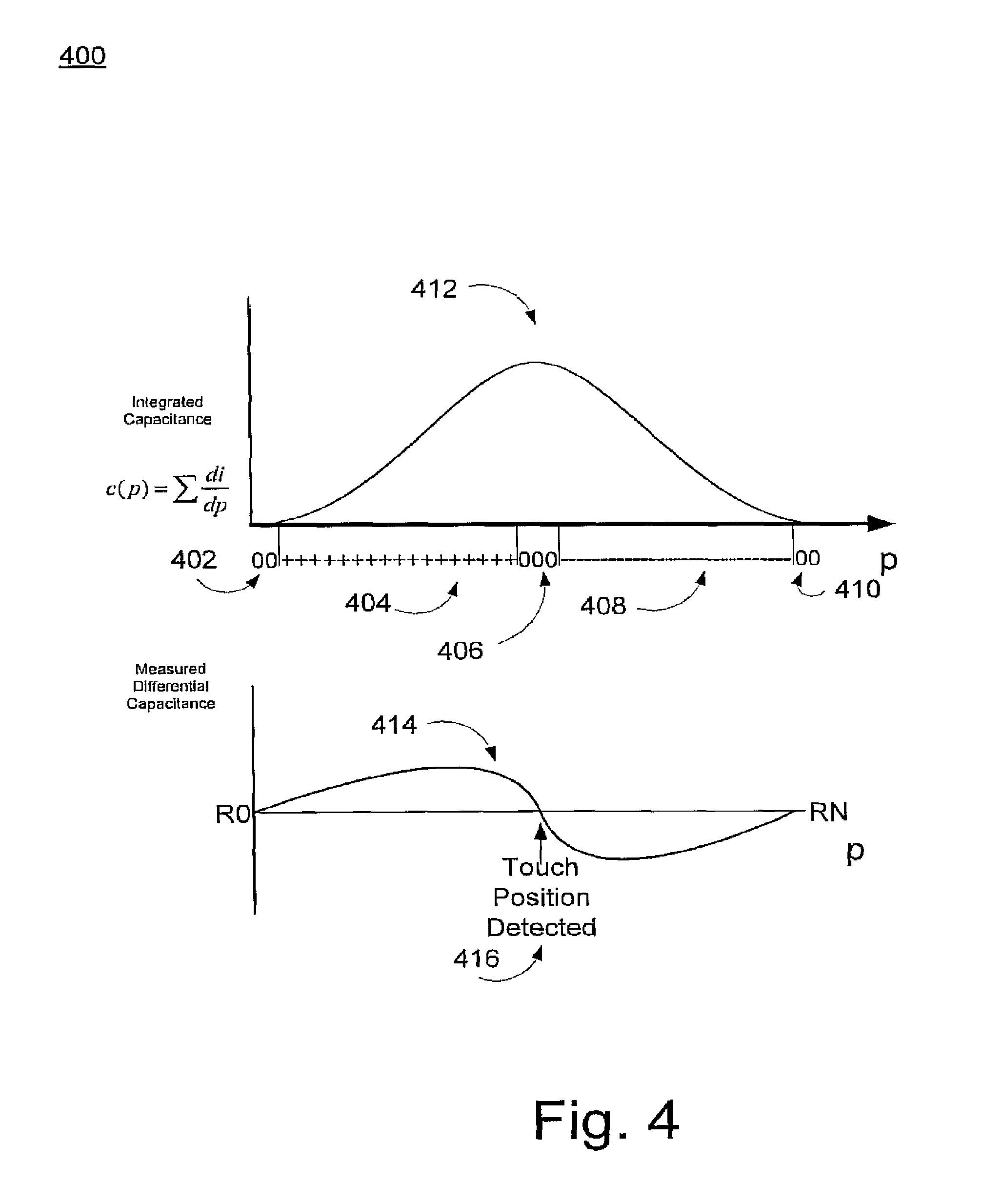
8. The method of claim 1, wherein said measured capacitance excludes a contribution from uniform variations in said capacitive sensor array.
9. The method of claim 1, wherein said comparison of the first and second currents is performed by a differential current measurement circuit.
10. The method of claim 1, wherein said capacitive sensor array comprises N electrodes disposed along a first axis and said measuring of said capacitance is performed N-1 times per electrode along a second axis.
11. An apparatus to determine location of an object proximate to a capacitive sensor array, the apparatus comprising: a first input coupled to a first electrode of a capacitive sensor array; a second input coupled to a second electrode of the capacitive sensor array; a third input coupled to a third electrode of the capacitive sensor array, wherein the second electrode and the third electrode intersect with the first electrode of the capacitive sensor array; a receive circuit coupled to the first, second and third inputs, the receive circuit configured to receive a first current associated with a capacitance of the first and second electrodes, the first current induced on the second electrode by a drive signal applied to the first electrode and capacitively coupled to the second electrode, and a second current associated with another capacitance of the first and third electrodes, the second current induced on the third electrode by the drive signal applied to the first electrode and capacitively coupled to the third electrode; a compare circuit configured to compare capacitance between the second and third electrodes represented by the first and second currents, wherein the capacitance is converted a digital value representative of the result of the comparison of the first and second currents; and a processor configured to determine a location of an object proximate to the capacitive sensor array, based on a differential capacitance represented by a difference between the first and second currents.
12. The apparatus of claim 11, wherein the second and third electrodes are adjacent.
13. The apparatus of claim 11, wherein the first electrode is disposed along an axis orthogonal to an axis on which the second and third electrodes are disposed.
14. The apparatus of claim 11, wherein the second electrode is separated from the third electrode by at least one other electrode.
15. The apparatus of claim 11, wherein the determining the location of the object, based on the differential capacitance is configured to detect a presence of the object proximate to the capacitive sensor array.
16. The apparatus of claim 11, wherein the compare circuit is configured to measure a plurality of capacitances over a plurality of electrodes disposed along a second axis of the first electrode disposed along a first axis, and the processor is configured to integrate the plurality of capacitances to obtain integrated capacitance values, and use the integrated capacitance values to determine the location.
17. The apparatus of claim 11, wherein the differential capacitance excludes a contribution from uniform variations in the capacitive sensor array.
18. The apparatus of claim 11, wherein the compare circuit includes a differential current measurement circuit.
19. The apparatus of claim 11, wherein said capacitive sensor array comprises N electrodes disposed along a first axis and a comparing of said capacitance by the compare circuit is performed N -1 times per electrode along a second axis.
20. A system for determining position information comprising: a sensor array controller for selecting each of a first plurality of electrodes disposed along a first axis and each of a second plurality of electrodes disposed along a second axis for measuring a capacitance, wherein each of the second plurality of electrodes receives an induced current from a signal applied to at least one of the first plurality of electrodes and capacitively coupled to each of the second plurality of electrodes, wherein the induced current on each of the second plurality of electrodes is converted to a digital value by an integration circuit, the digital value representative of the signal and the capacitive coupling between the at least one of the first plurality of electrodes and each of the second plurality of electrodes, wherein said capacitance comprises the difference in capacitance between two of said second plurality of electrodes and at least one of said of second plurality of electrodes; a capacitive sensor array operable to be controlled by said sensor array controller and operable to respond to a presence of an object proximate to said sensor array; a data storage module for storing a plurality of capacitive measurements from said sensor array controller; and a data processing module for processing said plurality of capacitive measurements to determine a position of said object proximate to said capacitive sensor array.
Description
FIELD OF INVENTION
Embodiments of the present invention generally relate to touch sensitive sensor arrays.
BACKGROUND OF THE INVENTION
As computing technology has developed, user interface devices have advanced correspondingly. User interfaces have become increasingly significant in the usability of a computing device.
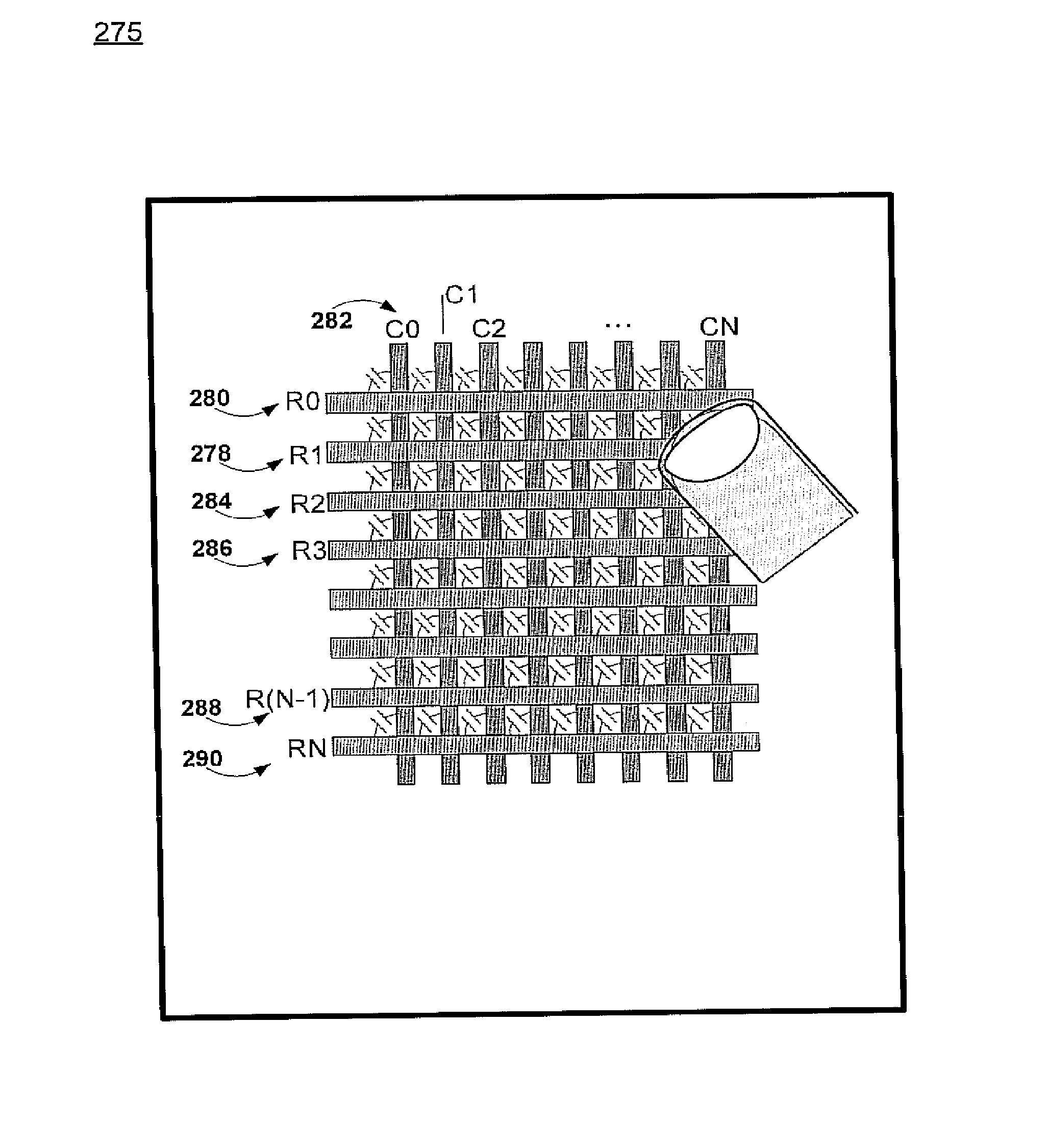
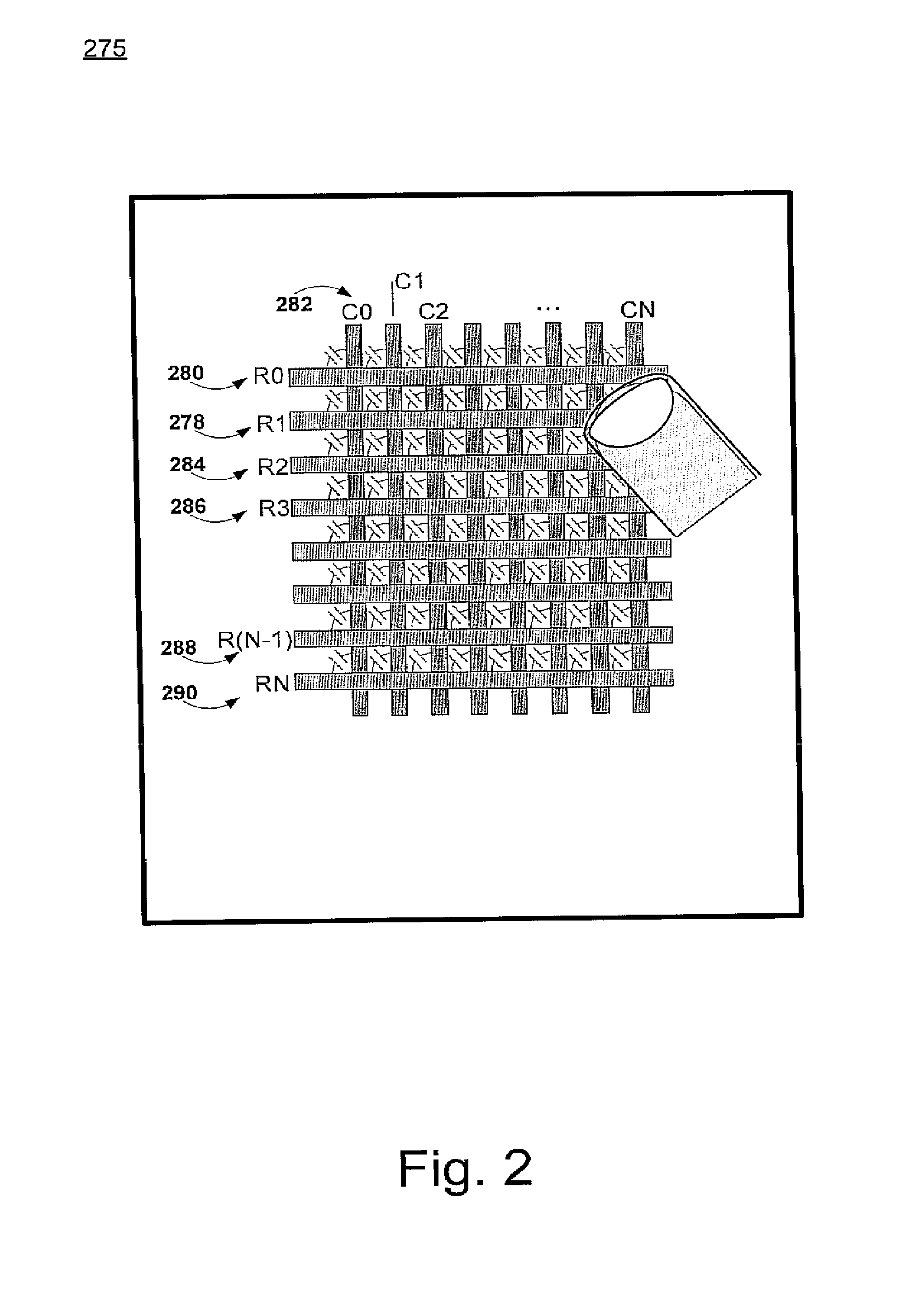
One particular user interface becoming increasingly popular is the touch screen or track pad which uses an array of capacitive sensors using high impedance capacitance substrates. The current, based on the change of the capacitance at the intersection of a row and a column of the array, which varies depending on the presence or absence of a touch, e.g., a finger, etc.
Row and/or columns are scanned sequentially and independently, one by one across the array by a microprocessor. The microprocessor may start by measuring the capacitance at a first column and a first row, then measuring the capacitance for the intersection of the first column and a second row, and then measuring each subsequent intersection in the capacitive sensor array. Thus, if there are 10 rows and 10 columns, a total of 100 measurements of capacitance may be obtained and stored by the microprocessor. Based on the measurements, a centroid corresponding to the finger location may then determined by the microprocessor.
Measuring of each intersection of each row and column may result in the measurements being subject to variations in the physical properties of the sensor array. For example, temperature changes can increase or decrease the capacitance.
Further, measuring capacitance means that the measured range with includes the absolute value of the capacitance. For example, if the capacitance is 8 picofarads (pF) without a finger present and a capacitance of 8.1 pF indicates a touch, the measurement circuit may be calibrated to measure a range of 1 to 10 pF for instance while the dynamic range is only 0.1. This leads to low resolution. The centering of the measurement window by using current compensation may avoid this low resolution. The current compensation involves using a current source to balance out or subtract the base capacitance. The current source is used to provide a current based on the baseline capacitance and thereby subtract out the baseline capacitance from capacitance measurements. The microprocessor accesses and load the baseline values into a programmable current source before each measurement of each row and column intersection. This current compensation solution requires extra hardware which increases costs and is slower as additional operations and settling times increase the time for each scan.
Thus, conventional capacitive sensor systems are susceptible to capacitive variations and utilize ground referenced capacitive measurements resulting in less accurate position information.
SUMMARY OF THE INVENTION
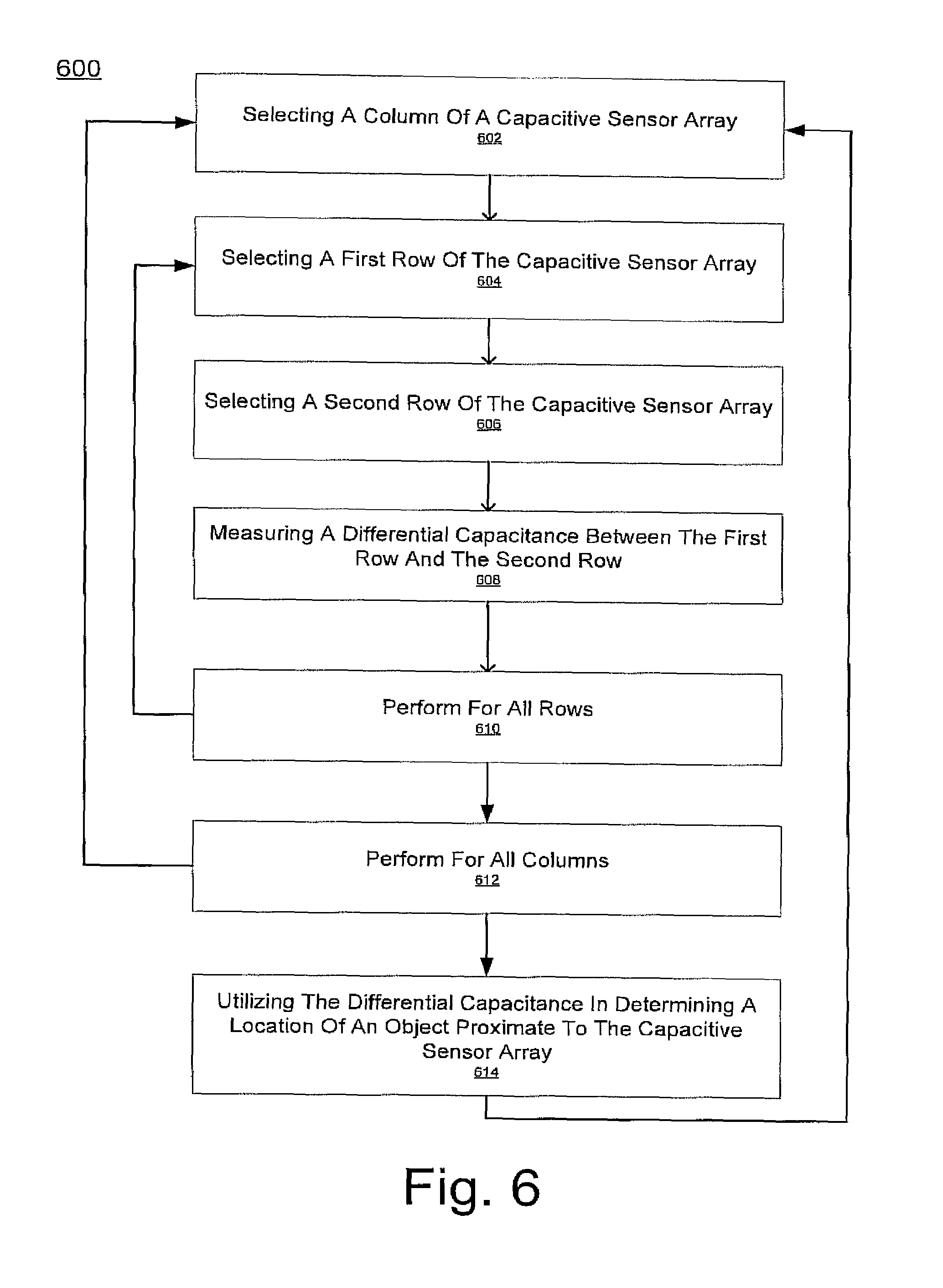
Accordingly, embodiments of the present invention are directed to a system and method for determining position information e.g., with respect to a touch sensitive array. Position information is determined based on differential capacitance measurements in one embodiment. The differential capacitance measurements may be with respect to adjacent rows and/or columns of the array and are substantially immune to variations (e.g., temperature changes, dielectric changes, etc.) of a capacitive sensor array. The differential capacitive measurements further facilitate increased resolution and require fewer measurements thereby making scans faster and more precise.
More specifically, an embodiment of the present invention is directed to a method for determining position information. The method includes selecting a column, a first row, and a second row of a capacitive sensor array. The first row and second row intersect with the column of the capacitive sensor array. Further, the first and second row may be selected as an adjacent pair or a distant pair (e.g., separated by at least one other row). The method further includes measuring a differential capacitance between the first row and the second row and utilizing the differential capacitance in determining a location of an object proximate to the capacitive sensor array. The location of the object may be determined by computing capacitance values for each row and column intersection based on the differential capacitance measurements.
Another embodiment of the present invention is directed to a circuit or electronic system for determining position information. The system includes a sensor array controller for selecting each of a plurality of rows and each of a plurality of columns for measuring a differential capacitance. The differential capacitance may include the difference in capacitance between two adjacent rows and thus variations (e.g., temperature effects, dielectric variations, etc.) in the capacitive sensor array may be substantially removed. The capacitive sensor array is operable to be controlled by the sensor array controller for detecting a presence of an object proximate to the sensor array. The system further includes a data storage module for storing a plurality of differential capacitive measurements and a data processing module for processing the plurality of differential capacitive measurements to determine the position of an object proximate to a capacitive sensor array.
In one embodiment, the circuit for measuring the capacitance across two rows or columns is differential in nature thereby leading to a direct differential measurement which is supplied to a processor for position determination. By eliminating the base capacitance of the array in this fashion, more resolution applied via the capacitive sensor to the expected dynamic range for a touch. In another embodiment, however, absolute capacitance measurements can be taken and supplied to the processor which computes the different values via software.
In this fashion, embodiments of the present invention facilitate more precise capacitance measurements and therefore more accurate object location detection. Embodiments of the present invention further facilitate simplified capacitive sensor array systems by removing the necessity for current compensation circuitry. Moreover, embodiments of the present invention allow more frequent scans by reducing the number of measurements performed for each column.
BRIEF DESCRIPTION OF THE DRAWINGS
FIG. 1 shows block a diagram of an exemplary system for determining position information, in accordance with one embodiment of the present invention.
FIG. 2 shows a block diagram of an exemplary capacitive sensor array, in accordance with another embodiment of the present invention.
FIG. 3 shows block diagram of an exemplary implementation of a system for determining position information, in accordance with an embodiment of the present invention.
FIG. 4 shows an exemplary graph of capacitance measurements, in accordance with an embodiment of the present invention.
FIG. 5 shows an exemplary system for determining position information, in accordance with an embodiment of the present invention.
FIG. 6 shows a flowchart of an exemplary method for determining position information, in accordance with an embodiment of the present invention.
DESCRIPTION OF THE INVENTION
Reference will now be made in detail to embodiments of the claimed subject matter, examples of which are illustrated in the accompanying drawings. While the invention will be described in conjunction with embodiments, it will be understood that they are not intended to limit the claimed subject matter to these embodiments. On the contrary, the claimed subject matter is intended to cover alternatives, modifications and equivalents, which may be included within the spirit and scope of the claimed subject matter as defined by the claims. Furthermore, in the detailed description of the present invention, numerous specific details are set forth in order to provide a thorough understanding of the claimed subject matter. However, it will be obvious to one of ordinary skill in the art that the claimed subject matter may be practiced without these specific details. In other instances, well known methods, procedures, components, and circuits have not been described in detail as not to unnecessarily obscure aspects of the claimed subject matter.
EXAMPLE SYSTEMS
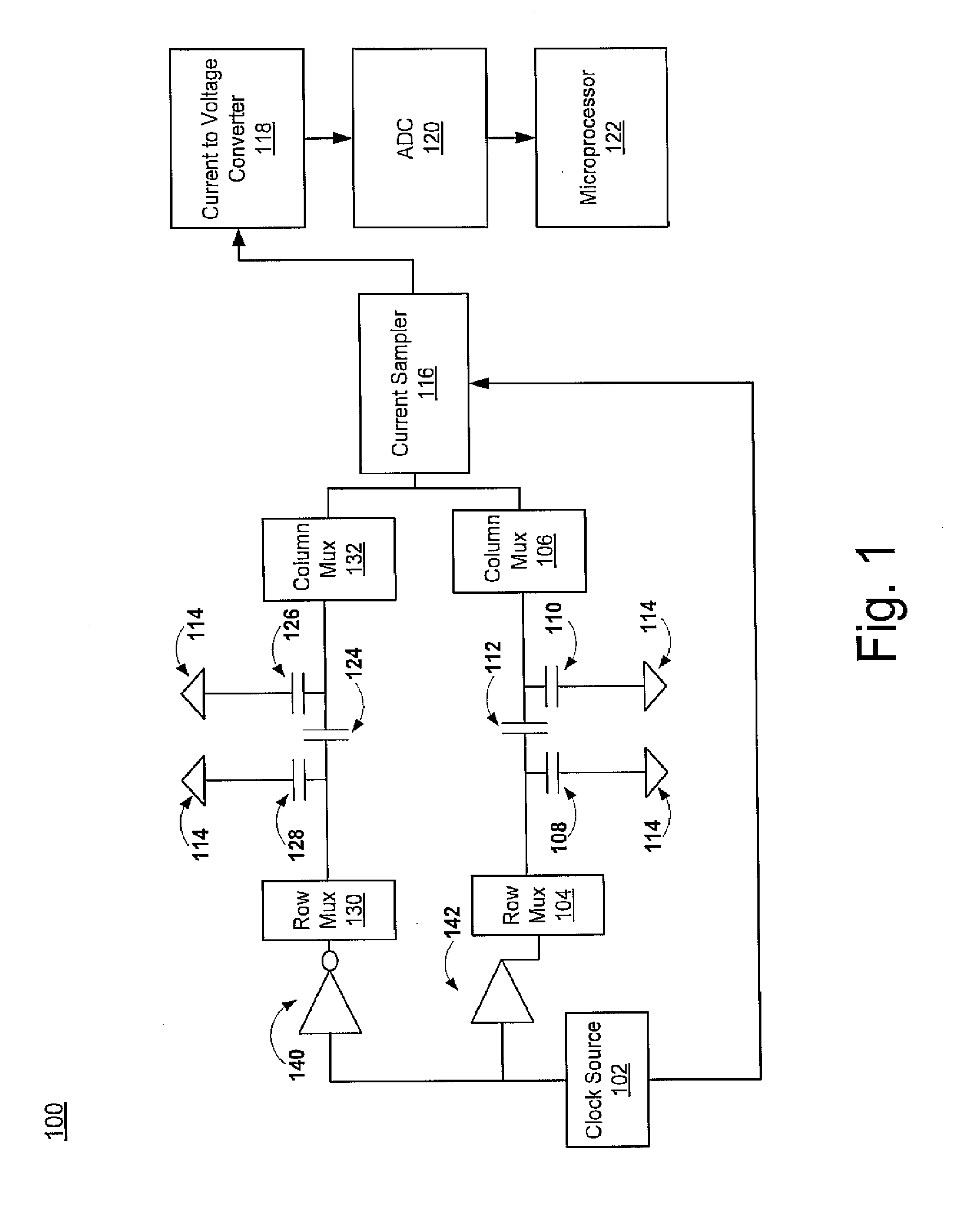
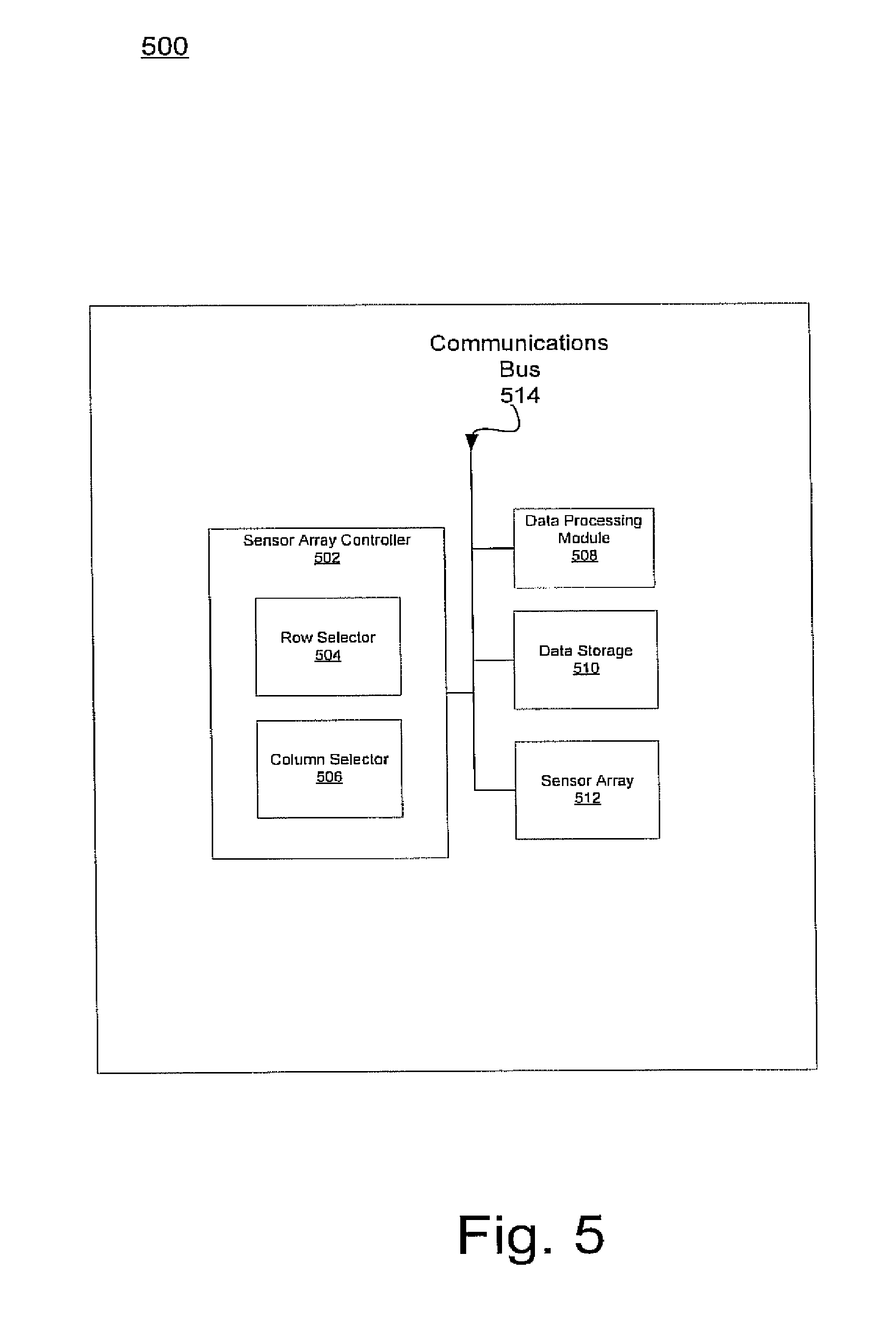
FIGS. 1, 3, and 5 illustrate example components used by various embodiments of the present invention. Although specific components are disclosed in circuits or systems 100, 300, and 500 it should be appreciated that such components are examples. That is, embodiments of the present invention are well suited to having various other components or variations of the components recited in systems 100, 300, and 500. It is appreciated that the components in systems 100, 300, and 500 may operate with other components than those presented, and that not all of the components of systems 100, 300, and 500 may be used to achieve the goals of systems 100, 300, and 500.
Further, systems 100, 300, and 500 include components or modules that, in various embodiments, are carried out by software, e.g., a processor under the control of computer-readable and computer-executable instructions. The computer-readable and computer-executable instructions reside, for example, in data storage features such as computer usable memory, removable storage, and/or non-removable storage. The computer-readable and computer-executable instructions are used to control or operate in conjunction with, for example, a processing unit It should be appreciated that the aforementioned components of systems 100, 300, and 500 can be implemented in hardware or software or in a combination of both.
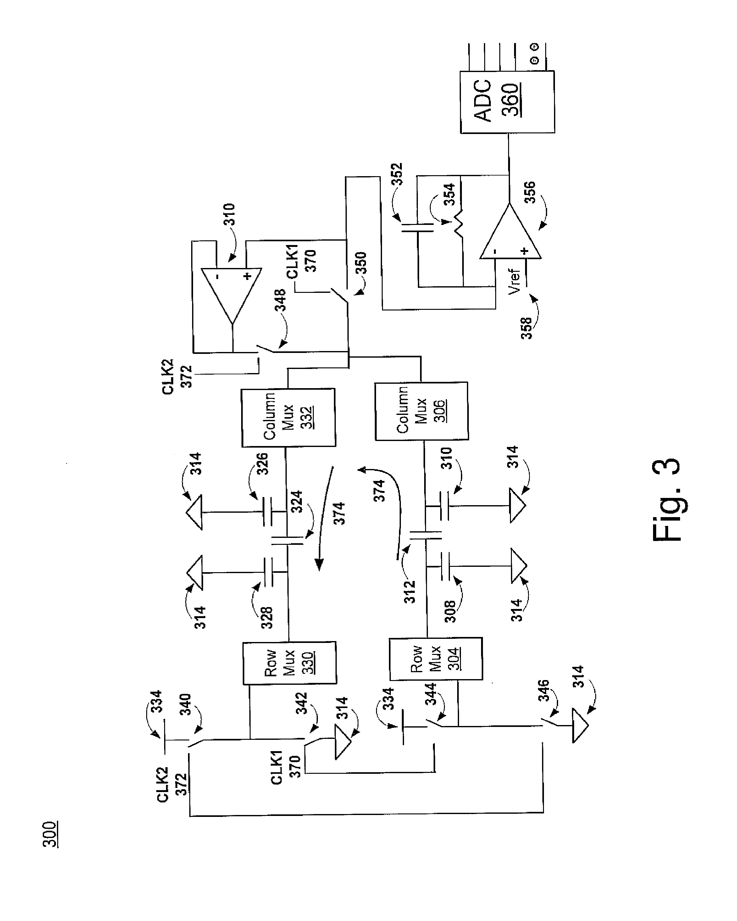
FIG. 1 shows block diagram of an exemplary system for determining position information, in accordance with another embodiment of the present invention. System 100 includes clock source 102, buffer 142, inverter 140, row multiplexers 104 and 130, column multiplexers 106 and 132, row capacitors 108 and 128, column capacitors 110 and 126, measurement capacitors 112 and 124, current sampler 116, current to voltage converter 118, analog to digital converter (ADC) 120, and microprocessor 122. System 100 measures the differential current based on the difference in capacitance of measurement capacitors 112 and 124.
Clock source 102 is coupled to buffer 142, inverter 140, and current sampler 116. Buffer 142 is coupled to row multiplexer 104. Inverter 140 is coupled to row multiplexer 130. Row multiplexers 104 and 130 thus receive clock signals. The selection of rows and columns via row multiplexers 130 and 104 and column multiplexers 106 and 132 allows current sampler 116 to measure a differential current between two rows of a capacitive sensor array. It is appreciated that clock source 102, buffer 142, and inverter 140 may be interchanged with a component having an inverting and non-inverting state. It is further appreciated that the coupling of current sampler 116 and clock source 102 may be optional or current sampler 116 may be coupled to a microprocessor (e.g., microprocessor 122) or some external control.
In one embodiment, current sampler 116 provides synchronous rectification which is represented by a switch which becomes closed only on the positive transition of a clock signal from clock source 102. Current sampler 116 may be a switching circuit. Current to voltage converter 118 converts the measured current to a voltage for input to ADC 120. ADC 120 converts the analog voltage to a digital signal for input to microprocessor 122.
Microprocessor 122 controls row multiplexers 104 and 130 and column multiplexers 106 and 132, sets conversion times and collects the data from the capacitive sensor array. Microprocessor 122 may utilize column multiplexers 106 and 132 to select a single column of capacitive sensor array (e.g., an indium tin oxide (ITO) sensor array) and utilizes row multiplexers 104 and 130 to select a pair of rows. Of course the role of columns and rows can be switches in accordance with embodiments of the present invention and any discursion herein regarding a particular scan order is merely a convenience for illustration. The selection of two different rows in combination with the clock signal and inverted clock signal (e.g., via inverter 140) allows current to flow in opposite directions though measurement capacitors 112 and 124. The opposite current flow results in a current difference flowing into current sampler 116. That is, current sampler 116 receives the summation of the currents (e.g., in opposite directions) or a differential current. This differential current reflects the difference in the capacitance of measurement capacitors 112 and 124. For example, if the capacitance of capacitor 112 is greater than the capacitance of capacitor 124, there will be a net positive current remaining and measured by the current sampler 116.
The differential current measured is independent of physical variations on the capacitive sensor array that are common to both measured capacitors. For example, a temperature variation which uniformly impacts the capacitive sensor arrays may be substantially cancelled because both measurements capacitors 112 and 124 will include the noise signal which thereby will be subtracted out. Similarly, physical variations (e.g., dielectric changes caused by temperature changes, etc.) that impact the array in general are substantially removed from the differential current measurements.
The measuring of differential currents thereby reduces the corresponding dynamic range of the measurement chain. Due to the differential nature of the current measurements only the differences are measured which means the total dynamic range of the measurement circuit may be much smaller and more finely tuned to the range of expected capacitance variations of a touch. That is, embodiments of the present invention provide for zero current centered measurements. For example, where the difference in capacitance (as measured based on the current) is 0.1 pF to register a touch instead of an absolute measurement of 8.1 pF, the dynamic range can be tuned to measure small variations (e.g., a range of 0-0.5 pF instead of 0-10 pF). It is appreciated that the differential measurements of embodiments of the present invention thereby remove the necessity of a current source and additional circuitry for providing current compensation. Embodiments of the present invention may thus be simpler and more reliable with increase resolution.
Further, the more finely tune dynamic range facilitates much higher resolution. For example, if ADC 220 has 10 output bits for communicating a value to microprocessor, with embodiments of the present invention the 10 bits may be used to communicate values with a range of 1 pF instead of a range of 5 or 10 pF. Accordingly, embodiments of the present invention facilitate increased accuracy and resolution of measurements.
In one embodiment, the pairs of rows may be adjacent as microprocessor 122 goes through each column of a capacitive sensor array. That is, microprocessor 122 may select pairs of adjacent rows for making differential measurements. For example, microprocessor 222 may select column C0, then obtain differential measurements between rows R0 and R1, then R1 and R2, the R2 and R3, all the way up to R(N-1) and R(N).
However, row measurements may not necessarily be across adjacent rows. In another embodiment, the pairs of rows may be distant (e.g., separated by at least one other row) as microprocessor 122 goes through each column of a capacitive sensor array. That is, microprocessor 122 may select a first row and measure a differential capacitance between the first row and each of the other rows of the capacitive sensor array for each column. For example, microprocessor may selected column C0, then get differential measurements between row R0 and R1, then row R0 and R2, then rows R0 and R3, all the way up to row R0 and RN. Embodiments of the present invention may further include an extra row and column to be used a control (e.g., baseline) for differential measurements, e.g., a dummy row.
The scanning of the rows in pairs results in N-1 measurements per each column in a capacitive sensory array having N rows. That is, the scanning of the rows in pairs means that one less measurement is made per column which decreases the time to scan the capacitive sensor array. For example, where a capacitive sensor array has 10 rows and 10 columns, 9 differential measurements for each of the 10 columns will be made. This results in a total of 90 (e.g., 9 differential measurements.times.10 columns) differential measurements being made. It is appreciated that a measurement for each row and column intersection would result in 100 measurements (e.g., 10 rows.times.10 columns). More generally, a capacitive sensor array with N row and M columns will have N-1 measurements per column and N-1.times.M measurements in total in accordance with embodiments of the present invention.
Microprocessor 122 further analyzes the data from the capacitive sensor array. Based on the differential current measurements and corresponding differential capacitance values, microprocessor 122 can determine the centroid of an object relative to the capacitive sensor array. In one embodiment, microprocessor 122 integrates the differential capacitive values going down each column to create a curve of the total capacitance at each row and column intersection (e.g., See FIG. 4). The integration may be then used for position determination. The curve may be further adjusted by adding the absolute value of the lowest negative number to each capacitance value thereby shifting the curve up to assist in locating a centroid. In another embodiment, microprocessor 122 may execute a method of searching the differential values for locations where the differential values change from positive to negative (e.g., cross zero).
FIG. 2 shows block diagram of an exemplary capacitive sensor array, in accordance with another embodiment of the present invention. Capacitive sensor array 275 includes rows R0-RN and columns C0-CN. Multiplexers 104, 106, 130, and 132 may be used to select respective pairs of rows and columns as microprocessor 122 scans each pair of rows and the corresponding column intersection.
As described herein, scanning of capacitive sensor array 275 may be based on differential measurements of adjacent pairs (e.g., separated by at least one other row). For example, column C0 282 may be selected and differential measurements may be made with row R0 280 and row R1 278, then row R1 278 and row R2 284, then row R2 284 and row R3 286, all the way up to row R(N-1) 288 and row RN 290. As discussed herein, the roll of the columns and rows can be reverses in accordance with embodiments of the present invention.
As described herein, scanning of capacitive sensor array 275 may also be based on differential measurements of distant pairs (e.g., separated by at least one other row). For example, column C0 282 may be selected and differential measurements may be made with row R0 280 and row R1 278, then row R0 280 and row R2 284, then row R0 280 and row R3 286, all the way up to row R0 280 and row RN 290.
FIG. 3 shows block diagram of an exemplary implementation of a system for determining position information, in accordance with an embodiment of the present invention. System 300 includes clock1 370, clock2 372, voltage rail 334 (e.g., Vcc), row multiplexers 304 and 330, column multiplexers 306 and 332, row capacitors 308 and 328, column capacitors 310 and 326, measurement capacitors 312 and 324, switches 340-350, amplifiers 310 and 356, resistor 354, capacitor 352, reference voltage (Vref) 358, and analog to digital converter (ADC) 360. Circuit 300 measures the differential current based on the difference in capacitance of measurement capacitors 312 and 324. Arrows 374 reflect an exemplary current flow.
System 300 operates in a substantially similar manner to system 200. Switches 342, 344, and 348 are coupled to clock1 370. Switches 340, 346, and 348 are coupled to clock2 372. It is appreciated that clock1 370 and clock2 372 may be inverses of each other. Row multiplexers 330 and 304 and column multiplexers 306 and 332 may be controlled by a microprocessor (e.g., microprocessor 222).
Amplifier 310 in combination with switches 348 and 350 acts a current sampler (e.g., current sampler 216) to sample differential current from measurement capacitors 312 and 324. The differential current measurement signal then passes to capacitor 352, resistor 354, and amplifier 358. Amplifier 358 has reference voltage (Vref) 358 as an input. The combination of capacitor 352, resistor 354, and amplifier 358 acts to convert the current to a voltage for input to ADC 360. ADC 360 may then convert the voltage to a digital signal for input to a microprocessor (e.g., microprocessor 222).
FIG. 4 shows an exemplary graph of capacitance measurements, in accordance with an embodiment of the present invention. Each graph includes a vertical axis corresponding to the capacitance and horizontal axis corresponding to position(p) (e.g., row). Curve 414 corresponds to the measured differential capacitance for each position (e.g., row). A touch position is detected at position 416 where curve 414 crosses the axis. Line 412 represents exemplary capacitance values measured over a plurality of row and column intersections (e.g., for a give column). Line 412 may be expressed by the equation:
.function.dd ##EQU00001## Where
dd ##EQU00002## is the differential capacitance measured at each row and column intersection for the given column and reported to the processor. The function f(p) is the summation of each
dd ##EQU00003## which results in the capacitance values as depicted by line 412. The function f(p) may correspond to the capacitance values for a single column. The summation or integration may be performed by a processor (e.g., processor 122). Further, the processor detects a touch position by analyzing the curve of the function f(p).
Regions 402 and 410 corresponds to areas where the differential capacitive measurements have minimal to zero difference and may correspond to row and column intersections where an object (e.g., finger) is not present.
Region 406 corresponds to an area where the capacitance on each measurement capacitor (e.g., measurement capacitors 212 and 224) is substantially similar where there is no object nearby and thus the differential capacitance is minimal or zero. Region 406 may correspond to the centroid where an object is present over or on top of a capacitive sensor array (e.g., capacitive sensor array 275). Region 404 corresponds to locations where the differential capacitance is increasing (e.g., the row and column intersections on the edge of an object).
Region 408 corresponds to locations where the differential capacitance is decreasing (e.g., the row and column intersections on the edge of an object). It is appreciated that the increasing or decreasing nature of the differential capacitive values may be based on the selection of current flow (e.g., as depicted in FIG. 3).
FIG. 5 shows an exemplary system for determining position information, in accordance with an embodiment of the present invention. System 500 includes sensor array controller 502, data processing module 508, data storage 510, sensor array 512, and communications bus 514. The blocks of system 500 may be carried out or performed by system for determining position information (e.g., system 100 or 300). Capacitive sensor array 512 is operable to be controlled by the sensor array controller for detecting the presence of an object proximate to the sensor array.
Sensor array controller 502 selects each of a plurality of rows and each of a plurality of columns for measuring a differential capacitance. Sensor array controller 502 includes row selector 504 and column selector 506. Sensor array controller 502 may use the column selector 506 to select each column of capacitive sensor array and use row selector 504 to select pairs of row for measuring differential capacitances. It is appreciated that embodiments of the present invention may also select a row and pairs of columns.
As described herein, the differential capacitance may be measured by a pair of adjacent rows or a pair of distant rows (e.g., rows separated by at least one other row). For example, differential capacitances may be measured for row 0 and row 1, row 1 and row 2, and so on in adjacent pairs until row N-1 and row N for a capacitive sensor array having N rows. As another example, differential capacitances may be measured for row 0 and row 1, row 0 and row 2, and so on with row 0 being paired with successive rows until row 0 is paired with row N for a capacitive sensory array having N rows. As described herein, the measuring of differential capacitances for pairs of rows allows sensor array controller to make N-1 measurements per column for a capacitive sensor array having N rows.
Further, as described herein, the differential measurements performed by embodiments resulting the capacitance measurements being substantially immune to common mode variations in the capacitive sensor array. The differential measurements facilitate increased resolution as the range of measurement can be calibrated accordingly to the capacitance change instead of the absolute capacitance value (e.g., capacitance with respect to ground).
Data storage module 510 stores a plurality of differential capacitive measurements. As described herein, a plurality of differential capacitive measurements may be made for each pair of rows in a capacitive sensor array.
Data processing module 508 processes a plurality of differential capacitive measurements to determine the position of an object proximate to a capacitive sensor array. As described herein, data processing module 508 may be operable to compute capacitance values for each row and column intersection of the capacitive sensor array based on the differential capacitance measurements.
EXAMPLE OPERATIONS
With reference to FIG. 6, exemplary flowchart 600 illustrates example blocks used by various embodiments of the present invention. Although specific blocks are disclosed in flowchart 600, such blocks are examples. That is, embodiments are well suited to performing various other blocks or variations of the blocks recited in flowchart 600. It is appreciated that the blocks in flowchart 600 may be performed in an order different than presented, and that not all of the blocks in flowchart 600 may be performed. Flowchart 600 includes processes that, in various embodiments, are carried out by a processor under the control of computer-readable and computer-executable instructions. Embodiments of the present invention may thus be stored as computer readable media or computer-executable instructions including, but not limited to, a firmware update, software update package, or hardware (e.g., ROM).
In particular, FIG. 6 shows a flowchart of an exemplary process for determining position information, in accordance with an embodiment of the present invention. Blocks of flow chart 600 may be carried out by modules of system (e.g., system 500) for determining position information.
At block 602, a column of a capacitive sensor array is selected. At block 604, a first row of the capacitive sensor array is selected. At block 606, a second row of the capacitive sensor array is selected. The first row and the second row intersect with the selected column of the capacitive sensor array. In one embodiment, the first row and the second row are adjacent. In another embodiment, the first and second row may be distant from one another (e.g., separated by at least one other row).
At block 608, a differential capacitance between the first row and the second row is measured. As described herein, the differential capacitance is independent of variations in the capacitive sensor array. Further, the differential capacitance facilitates increased resolution as the measurements are zero centered. The measuring of the differential capacitances facilitates quicker scans because the differential measurements are performed N-1 times per column for a capacitive sensor array comprising N rows.
At block 610, a check is performed to determine if the differential measurements have been performed for all rows. If there are rows remaining in a column to be measured block 604 is performed. If there are no more rows remaining, block 612 may be performed.
At block 612, a check is performed to determine if the differential measurements have been performed for all columns. If there are columns remaining to be measured block 604 is performed. If there no more columns remaining to be measured, block 614 may be performed.
At block 614, the differential capacitance is utilized in determining a location of an object proximate to the capacitive sensor array. As described herein, the differential capacitances are operable to be used to compute capacitance values for each row and column intersection of the capacitive sensor array (e.g., FIG. 4).
Thus, embodiments of the present invention facilitate more accurate capacitance measurements which are immune to capacitive sensor variations (e.g., temperature changes, dielectric property changes, etc.). Embodiments of the present invention further provide increased resolution and zero centered measurements thereby making current compensation circuitry unnecessary for tuning the dynamic range of the measurements. The measuring of differential capacitances by embodiments of the present invention allows for faster scanning of a capacitive sensor array by performing one less measurement per column.
Embodiments of the present invention are thus described. While the present invention has been described in particular embodiments, it should be appreciated that the present invention should not be construed as limited by such embodiments, but rather construed according to the below claims.
* * * * *
References
D00000
D00001
D00002
D00003
D00004
D00005
D00006
M00001
M00002
M00003
XML
uspto.report is an independent third-party trademark research tool that is not affiliated, endorsed, or sponsored by the United States Patent and Trademark Office (USPTO) or any other governmental organization. The information provided by uspto.report is based on publicly available data at the time of writing and is intended for informational purposes only.
While we strive to provide accurate and up-to-date information, we do not guarantee the accuracy, completeness, reliability, or suitability of the information displayed on this site. The use of this site is at your own risk. Any reliance you place on such information is therefore strictly at your own risk.
All official trademark data, including owner information, should be verified by visiting the official USPTO website at www.uspto.gov. This site is not intended to replace professional legal advice and should not be used as a substitute for consulting with a legal professional who is knowledgeable about trademark law.