ALD metal coatings for high Q MEMS structures
Kubena , et al.
U.S. patent number 10,266,398 [Application Number 14/555,459] was granted by the patent office on 2019-04-23 for ald metal coatings for high q mems structures. This patent grant is currently assigned to HRL Laboratories, LLC. The grantee listed for this patent is HRL Laboratories, LLC. Invention is credited to Richard J. Joyce, Randall L. Kubena.


View All Diagrams
| United States Patent | 10,266,398 |
| Kubena , et al. | April 23, 2019 |
ALD metal coatings for high Q MEMS structures
Abstract
A method for fabricating a Microelectromechanical System (MEMS) resonator includes providing a dielectric substrate defining a resonator and depositing a conductive coating having a resistivity of approximately 1 to 50 .mu..OMEGA.-cm on that substrate by Atomic Layer Deposition (ALD). A resonator fabricated according to this process includes a dielectric substrate defining a resonator and a conductive coating having a resistivity of approximately 1 to 50 .mu..OMEGA.-cm for electrically coupling the resonator to electronics. Another method for fabricating a MEMS resonator includes providing a dielectric substrate defining a resonator, depositing an aluminum oxide film on that substrate by ALD, and depositing a noble metal film on the aluminum oxide film, also by ALD.
| Inventors: | Kubena; Randall L. (Oak Park, CA), Joyce; Richard J. (Thousand Oaks, CA) | ||||||||||
|---|---|---|---|---|---|---|---|---|---|---|---|
| Applicant: |
|
||||||||||
| Assignee: | HRL Laboratories, LLC (Malibu,
CA) |
||||||||||
| Family ID: | 66174702 | ||||||||||
| Appl. No.: | 14/555,459 | ||||||||||
| Filed: | November 26, 2014 |
Related U.S. Patent Documents
| Application Number | Filing Date | Patent Number | Issue Date | ||
|---|---|---|---|---|---|
| 13363174 | Jan 31, 2012 | ||||
| 13648041 | Jun 21, 2015 | 9046541 | |||
| 12488784 | Jul 1, 2014 | 8766745 | |||
| 12179579 | Jul 24, 2008 | ||||
| 61082125 | Jul 18, 2008 | ||||
| 60962176 | Jul 25, 2007 | ||||
| 60973703 | Sep 19, 2007 | ||||
| Current U.S. Class: | 1/1 |
| Current CPC Class: | B81B 3/0078 (20130101); C23C 16/18 (20130101); C23C 16/045 (20130101); B81C 1/00206 (20130101); C23C 16/45525 (20130101); B81B 3/0086 (20130101); C23C 16/403 (20130101); C23C 16/06 (20130101); C23C 16/45555 (20130101); B81B 2201/0242 (20130101); B81B 2201/0271 (20130101); B81C 2201/0181 (20130101) |
| Current International Class: | H03H 9/02 (20060101); C23C 16/455 (20060101); B81C 1/00 (20060101); H03H 9/24 (20060101); C23C 16/06 (20060101) |
| Field of Search: | ;73/503.3 ;427/250,395,255.7 ;438/15,55,64,106,6 |
References Cited [Referenced By]
U.S. Patent Documents
| 392650 | November 1888 | Watrous |
| 2487165 | November 1949 | Miller |
| 3390287 | June 1968 | Hans |
| 3766616 | October 1973 | Staudte |
| 4364016 | December 1982 | Tanski |
| 4426769 | January 1984 | Grabbe |
| 4442574 | April 1984 | Wanuga et al. |
| 4447753 | May 1984 | Ochiai |
| 4618262 | October 1986 | Maydan et al. |
| 4870313 | September 1989 | Hirama et al. |
| 4898031 | February 1990 | Oikawa et al. |
| 4944836 | July 1990 | Beyer et al. |
| 5203208 | April 1993 | Bernstein |
| 5226321 | July 1993 | Varnham et al. |
| 5260596 | November 1993 | Dunn et al. |
| 5421312 | June 1995 | Dawson |
| 5480747 | January 1996 | Vasudev |
| 5530408 | June 1996 | Vig et al. |
| 5552016 | September 1996 | Ghanayem |
| 5578976 | November 1996 | Yao et al. |
| 5589724 | December 1996 | Satoh et al. |
| 5604312 | February 1997 | Lutz |
| 5605490 | February 1997 | Laffey et al. |
| 5644139 | July 1997 | Allen |
| 5646346 | July 1997 | Okada |
| 5648849 | July 1997 | Canteloup et al. |
| 5658418 | August 1997 | Coronel et al. |
| 5665915 | September 1997 | Kobayashi et al. |
| 5666706 | September 1997 | Tomita et al. |
| 5668057 | September 1997 | Eda et al. |
| 5728936 | March 1998 | Lutz |
| 5783749 | July 1998 | Lee et al. |
| 5894090 | April 1999 | Tang et al. |
| 5905202 | May 1999 | Kubena et al. |
| 5920012 | July 1999 | Pinson |
| 5928532 | July 1999 | Koshimizu et al. |
| 5942445 | August 1999 | Kato et al. |
| 5959206 | September 1999 | Ryrko |
| 5981392 | November 1999 | Oishi |
| 5987985 | November 1999 | Okada |
| 6009751 | January 2000 | Ljung |
| 6044705 | April 2000 | Neukermans et al. |
| 6049702 | April 2000 | Tham |
| 6081334 | June 2000 | Grimbergen et al. |
| 6094985 | August 2000 | Kapels et al. |
| 6114801 | September 2000 | Tanaka et al. |
| 6145380 | November 2000 | MacGugan et al. |
| 6151964 | November 2000 | Nakajima |
| 6155115 | December 2000 | Ljung |
| 6164134 | December 2000 | Cargille |
| 6182352 | February 2001 | Deschenes et al. |
| 6196059 | March 2001 | Kosslinger |
| 6204737 | March 2001 | Ella |
| 6207008 | March 2001 | Kijima |
| 6236145 | May 2001 | Biernacki |
| 6250157 | June 2001 | Touge |
| 6263552 | July 2001 | Takeuchi et al. |
| 6282958 | September 2001 | Fell et al. |
| 6289733 | September 2001 | Challoner et al. |
| 6297064 | October 2001 | Koshimizu |
| 6349597 | February 2002 | Folkmer et al. |
| 6367326 | April 2002 | Okada |
| 6367786 | April 2002 | Gutierrez et al. |
| 6413682 | July 2002 | Shibano et al. |
| 6417925 | July 2002 | Naya |
| 6424418 | July 2002 | Kawabata et al. |
| 6426296 | July 2002 | Okojie |
| 6432824 | August 2002 | Yanagisawa |
| 6481284 | November 2002 | Geen et al. |
| 6481285 | November 2002 | Shkel et al. |
| 6492195 | December 2002 | Nakanishi |
| 6513380 | February 2003 | Reeds et al. |
| 6514767 | February 2003 | Natan |
| 6515278 | February 2003 | Wine et al. |
| 6571629 | June 2003 | Kipp |
| 6584845 | July 2003 | Gutierrez et al. |
| 6614529 | September 2003 | Tang |
| 6621158 | September 2003 | Martin et al. |
| 6627067 | September 2003 | Branton et al. |
| 6628177 | September 2003 | Clark et al. |
| 6629460 | October 2003 | Challoner |
| 6651027 | November 2003 | McCall |
| 6710681 | March 2004 | Figueredo |
| 6715352 | April 2004 | Tracy |
| 6744335 | June 2004 | Ryhanen |
| 6750728 | June 2004 | Takahashi et al. |
| 6756304 | June 2004 | Robert |
| 6768396 | July 2004 | Klee |
| 6796179 | September 2004 | Bae et al. |
| 6806557 | October 2004 | Ding |
| 6815228 | November 2004 | Usui et al. |
| 6856217 | February 2005 | Clark et al. |
| 6862398 | March 2005 | Elkind et al. |
| 6883374 | April 2005 | Fell et al. |
| 6915215 | July 2005 | M'Closkey et al. |
| 6933164 | August 2005 | Kubena |
| 6943484 | September 2005 | Clark et al. |
| 6944931 | September 2005 | Shcheglov et al. |
| 6985051 | January 2006 | Nguyen et al. |
| 7040163 | May 2006 | Shcheglov |
| 7057331 | June 2006 | Shimodaira et al. |
| 7118657 | October 2006 | Golovchenko et al. |
| 7152290 | December 2006 | Junhua et al. |
| 7168318 | January 2007 | Challoner et al. |
| 7211933 | May 2007 | Kawakubo |
| 7224245 | May 2007 | Song |
| 7232700 | June 2007 | Kubena |
| 7234214 | June 2007 | Xu |
| 7237315 | July 2007 | Kubena et al. |
| 7270884 | September 2007 | Lian |
| 7295088 | November 2007 | Nguyen |
| 7317354 | January 2008 | Lee |
| 7347095 | March 2008 | Shcheglov |
| 7401397 | July 2008 | Shcheglov |
| 7446628 | November 2008 | Morris, III |
| 7459099 | December 2008 | Kubena et al. |
| 7459992 | December 2008 | Matsuda et al. |
| 7479846 | January 2009 | Inoue |
| 7490390 | February 2009 | Kawakubo et al. |
| 7493814 | February 2009 | Whelan |
| 7543496 | June 2009 | Ayazi |
| 7551054 | June 2009 | Mizuno |
| 7555824 | July 2009 | Chang |
| 7557493 | July 2009 | Fujimoto |
| 7559130 | July 2009 | Kubena et al. |
| 7564177 | July 2009 | Yoshimatsu |
| 7579748 | August 2009 | Kuroda |
| 7579926 | August 2009 | Jhung |
| 7581443 | September 2009 | Kubena |
| 7624494 | December 2009 | Challoner |
| 7663196 | February 2010 | Liu |
| 7671427 | March 2010 | Kim et al. |
| 7675224 | March 2010 | Tanaya |
| 7690095 | April 2010 | Takahashi |
| 7750535 | July 2010 | Kubena |
| 7757393 | July 2010 | Ayazi et al. |
| 7791431 | September 2010 | Piazza et al. |
| 7793541 | September 2010 | Challoner |
| 7802356 | September 2010 | Chang |
| 7830074 | November 2010 | Kubena |
| 7836765 | November 2010 | Challoner |
| 7872548 | January 2011 | Nishihara et al. |
| 7878064 | February 2011 | Abbott |
| 7884930 | February 2011 | Kirby |
| 7895892 | March 2011 | Aigner |
| 7958781 | June 2011 | Fell |
| 7987714 | August 2011 | DeNatale |
| 7994877 | August 2011 | Kubena |
| 8138016 | March 2012 | Chang |
| 8151640 | April 2012 | Kubena |
| 8176607 | May 2012 | Kubena |
| 8205495 | June 2012 | Challoner |
| 8322028 | December 2012 | Ge |
| 8381590 | February 2013 | Ikeda |
| 8393212 | March 2013 | Ge |
| 8522612 | September 2013 | Kubena |
| 8567041 | October 2013 | Roper |
| 8593037 | November 2013 | Kubena |
| 8766745 | July 2014 | Kubena |
| 8769802 | July 2014 | Chang et al. |
| 8782876 | July 2014 | Kubena et al. |
| 8912711 | December 2014 | Chang et al. |
| 9046541 | June 2015 | Kubena et al. |
| 2002/0066317 | June 2002 | Lin |
| 2002/0072246 | June 2002 | Goo et al. |
| 2002/0074947 | June 2002 | Tsukamoto |
| 2002/0107658 | August 2002 | McCall |
| 2002/0185611 | December 2002 | Menapace et al. |
| 2003/0003608 | January 2003 | Arikado et al. |
| 2003/0010123 | January 2003 | Malvern et al. |
| 2003/0029238 | February 2003 | Challoner |
| 2003/0196490 | October 2003 | Cardarelli |
| 2003/0205948 | November 2003 | Lin |
| 2004/0055380 | March 2004 | Shcheglov et al. |
| 2004/0055381 | March 2004 | Shcheglov |
| 2004/0065864 | April 2004 | Vogt et al. |
| 2004/0189311 | September 2004 | Glezer |
| 2004/0211052 | October 2004 | Kubena et al. |
| 2005/0034822 | February 2005 | Kim et al. |
| 2005/0062368 | March 2005 | Hirasawa |
| 2005/0093659 | May 2005 | Larson |
| 2005/0156309 | July 2005 | Fujii |
| 2005/0172714 | August 2005 | Challoner |
| 2005/0260792 | November 2005 | Patel |
| 2005/0274183 | December 2005 | Shcheglov |
| 2006/0016065 | January 2006 | Nagaura |
| 2006/0022556 | February 2006 | Bail et al. |
| 2006/0055479 | March 2006 | Okazaki et al. |
| 2006/0066419 | March 2006 | Iwaki |
| 2006/0139121 | June 2006 | Jhung |
| 2006/0162146 | July 2006 | Shcheglov |
| 2006/0197619 | September 2006 | Oishi et al. |
| 2006/0213266 | September 2006 | French |
| 2006/0252906 | November 2006 | Godschalx et al. |
| 2006/0255691 | November 2006 | Kuroda |
| 2007/0017287 | January 2007 | Kubena |
| 2007/0034005 | February 2007 | Acar |
| 2007/0084042 | April 2007 | Challoner |
| 2007/0205839 | September 2007 | Kubena et al. |
| 2007/0220971 | September 2007 | Ayazi |
| 2007/0240508 | October 2007 | Watson |
| 2008/0034575 | February 2008 | Chang et al. |
| 2008/0074661 | March 2008 | Zhang |
| 2008/0096313 | April 2008 | Patel |
| 2008/0148846 | June 2008 | Whelan |
| 2008/0295622 | December 2008 | Challoner |
| 2009/0095077 | April 2009 | DeNatale |
| 2009/0146527 | June 2009 | Lee |
| 2009/0189294 | July 2009 | Chang |
| 2010/0020311 | January 2010 | Kirby |
| 2010/0024560 | February 2010 | Shcheglov |
| 2010/0148803 | June 2010 | Ohnish |
| 2010/0251817 | October 2010 | Ge |
| 2010/0251818 | October 2010 | Ge |
| 2011/0107838 | May 2011 | Suijlen |
| 2012/0000288 | January 2012 | Matsuura |
| 2012/0212109 | August 2012 | Yamazaki |
| 2012/0266682 | October 2012 | Torashima |
| 4442033 | May 1996 | DE | |||
| 19719601 | Nov 1998 | DE | |||
| 461761 | Dec 1991 | EP | |||
| 0 531 985 | Mar 1993 | EP | |||
| 1055908 | Nov 2000 | EP | |||
| 971208 | Dec 2000 | EP | |||
| 57-091017 | Jun 1982 | JP | |||
| 401129517 | May 1989 | JP | |||
| 4322507 | Nov 1992 | JP | |||
| 5286142 | Nov 1993 | JP | |||
| 6232678 | Aug 1994 | JP | |||
| 6-318533 | Nov 1994 | JP | |||
| 8330878 | Dec 1996 | JP | |||
| 9-247025 | Sep 1997 | JP | |||
| 2003-318685 | Nov 2003 | JP | |||
| 2005-180921 | Jul 2005 | JP | |||
| 2006-352487 | Dec 2006 | JP | |||
| 10-2001-0110428 | Dec 2001 | KR | |||
| 84-00082 | Jan 1984 | WO | |||
| 96/38710 | Dec 1996 | WO | |||
| 98/15799 | Apr 1998 | WO | |||
| 00/68640 | Nov 2000 | WO | |||
| 01/44823 | Jun 2001 | WO | |||
| 01/74708 | Oct 2001 | WO | |||
| 02/12873 | Feb 2002 | WO | |||
| 2005/121769 | Dec 2005 | WO | |||
| 2006/010206 | Feb 2006 | WO | |||
| 2006/103439 | Oct 2006 | WO | |||
Other References
|
Ducument#1 http://hypertextbook.com/facts/2004/ValPolyakov.shtml, no date. cited by examiner . M. McNie et al, Microzyztem technologies 6(2000)184-188. cited by examiner . Jeffrey W. Elam et al, Journal of Nanomaterails vol. 2006, Article ID 64501, pp. 1-5, 2006. cited by examiner . U.S. Appl. No. 11/458,911, filed Jul. 20, 2006, Kubena et al. cited by applicant . U.S. Appl. No. 11/881,461, filed Jul. 27, 2007, Kubena et al. cited by applicant . U.S. Appl. No. 12/026,486, filed Feb. 5, 2008, Kubena. cited by applicant . U.S. Appl. No. 12/179,579, filed Jul. 24, 2008, Kubena. cited by applicant . U.S. Appl. No. 13/363,174, filed Jan. 31, 2012, Kubena et al. cited by applicant . Aaltonen, T., et al. "ALD of rhodium thin films from RH(acach and oxygen." Electrochemical and Solid-State Letters, 8{8), C99-C101 (2005). Laboratory of Inorganic Chemistry, Department of Chemistry, the University of Helsinki, Helsinki, Finland. cited by applicant . Abe,T., et al., "One-Chip Multichannel Quartz Crystal Microbalance (QCM) Fabricated by Deep RIE," Sensors and Actuators, 2000, pp. 139-143. cited by applicant . Barbour et al., "Micromechanical Silicon Instrument and Systems Development at Draper Laboratory," AIAA Guidance Navigation and Control Conference, 1996, Paper No. 96-3709. cited by applicant . Burdess et al., "The Theory of a Piezoelectric Disc Gyroscope", Jul. 1986, IEEE vol. AES 22, No. 4; p. 410-418. cited by applicant . Cleland, A.N., et al., "Fabrication of High Frequency Nanometer Scale Mechanical Resonators From Bulk Si Crystals," Applied Physics Letters, Oct. 28, 1996, pp. 2653-2655. cited by applicant . Evoy, S., et al., "Temperature-dependent Internal Friction in Silicon Nanoelectromechanical Systems," Applied Physics Letters, vol. 77, No. 15, Oct. 9, 2010. cited by applicant . Fujita et al., "Disk-shaped bulk micromachined gyroscope with vacuum sealing," Sensors and Actuators A:Physical, vol. 82, May 2000, pp. 198-204. cited by applicant . Greer, J.A., et al., "Properties of SAW resonators fabricated on quartz substrates of various qualities," Ultrasonics Symposium, 1994 IEEE, vol. 1, Nov. 1-4, 1994, pp. 31-36. cited by applicant . J.-M. Friedt and E. Carry, "Introduction to the quartz tuning fork", American Journal of Physics 75, 415 (2007), pp. 415-422. cited by applicant . Johnson et al., "Surface Micromachined Angular Rate Sensor," A1995 SAE Conference, Paper No. 950538, pp. 77-83. cited by applicant . Lin, J.W., et al., "A Robust High-Q Micromachined RF Inductor for RFIC Applications," IEEE Transactions on Electronic Devices, vol. 52, No. 7, pp. 1489-1496 (Jul. 2005). cited by applicant . Park, K.J. and Parsons, G.N. "Selective area atomic layer deposition of rhodium and effective work function characterization in capacitor structures." Applied Physics Letters, 89, pp. 043111-1 to 043111-3 (2006. cited by applicant . Putty et al., "A Micromachined Vibrating Ring Gyroscope," Solid State Sensor and Actuator Workshop, Transducer Research Foundation, Hilton Head, 1994, pp. 213-220. cited by applicant . Sirbuly, Donald J. et al., Multifunctional Nanowire Evanescent Wave Optical Sensors, Advanced Materials, 2007 (published online: Dec. 5, 2006), 19, pp. 61-66. cited by applicant . Skulski et al., "Planar resonator sensor for moisture measurements", Microwaves and Radar, 1998, MIKON '98, 12th International Conf., vol. 3, May 20-22, 1998, pp. 692-695. cited by applicant . Tang et al., "A Packaged Silicon MEMS Vibratory Gyroscope for Microspacecraft," Proceedings IEEE, 10th Annual Int. Workshop on MEMS, Japan, 1997, pp. 500-505. cited by applicant . Tang et al., "Silicon Bulk Micromachined Vibratory Gyroscope," Jet Propulsion Lab (6 pages). cited by applicant . White, Lan M., et al., Increasing the Enhancement of SERS with Dielectric Microsphere Resonators, Spectroscopy--Eugene, Apr. 2006. cited by applicant . Wright et al., "The HRG Applied to a Satellite Attitude Reference System," Guidance and Control, AASAAS, 1994, 86: pp. 55-67. cited by applicant . Yan, Fei, et al.,"Surface-enhanced Raman scattering (SERS) detection for chemical and biological agents," IEEE Sensors Journal, vol. 5, No. 4, Aug. 2005. cited by applicant . From U.S. Appl. No. 10/426,931 (now U.S. Pat. No. 7,237,315), Application and Office Actions including but not limited to the Office Actions dated Jun. 16, 2004, Aug. 31, 2004, Dec. 8, 2004, May 16, 2005, Aug. 11, 2005, Jan. 20, 2006, Jul. 11, 2006, Sep. 13, 2006, Oct. 24, 2006, and Feb. 1, 2007. cited by applicant . From U.S. Appl. No. 11/043,378 (now U.S. Pat. No. 7,459,099), Application and Office Actions, including but not limited to the Office Actions dated Aug. 11, 2006, Dec. 6, 2006, May 25, 2007, Sep. 12, 2007, Jan. 15, 2008, and Aug. 4, 2008. cited by applicant . From U.S. Appl. No. 11/458,911 (now U.S. Pat. No. 7,581,443), Application and Office Actions, including but not limited to the Office Actions dated Oct. 12, 2007, Apr. 17, 2008, Jul. 2, 2008, Sep. 17, 2008, and Apr. 23, 2009. cited by applicant . From U.S. Appl. No. 11/502,336 (now U.S. Pat. No. 7,555,824), Application and Office Actions, including but not limited to the Office Actions dated Nov. 14, 2008, Jan. 23, 2009, and Mar. 20, 2009. cited by applicant . From U.S. Appl. No. 11/800,289 (now U.S. Pat. No. 7,559,130), Application and Office Actions including but not limited to the Office Actions dated Oct. 24, 2008 and Mar. 25, 2009. cited by applicant . From U.S. Appl. No. 11/800,294 (now U.S. Pat. No. 7,750,535), Application and Office Actions, including but not limited to the Office Actions dated Jul. 29, 2009 and Nov. 30, 2009. cited by applicant . From U.S. Appl. No. 11/881,461 (now U.S. Pat. No. 7,830,074), Application and Office Actions, including but not limited to the Office Actions dated Jun. 16, 2009, Oct. 19, 2009, Jun. 2, 2010, Jul. 13, 2010, and Sep. 24, 2010. cited by applicant . From U.S. Appl. No. 12/027,247 (now U.S. Pat. No. 8,151,640), Application and Office Actions, including but not limited to the Office Actions dated Feb. 16, 2011, Jun. 7, 2011, and Dec. 8, 2011. cited by applicant . From U.S. Appl. No. 12/034,852 (now U.S. Pat. No. 7,802,356), Application and Office Actions, including but not limited to the Office Actions dated Oct. 2, 2009, Jan. 28, 2010, and May 19, 2010. cited by applicant . From U.S. Appl. No. 12/145,678 (now U.S. Pat. No. 7,884,930), Application and Office Actions, including but not limited to the Office Actions dated including those dated Jul. 22, 2009, Jan. 14, 2010, Mar. 26, 2010, and Jul. 13, 2010. cited by applicant . From U.S. Appl. No. 12/179,579, Application and Office Actions, including but not limited to the office action dated Dec. 9, 2010. cited by applicant . From U.S. Appl. No. 12/268,309 (now U.S. Pat. No. 7,994,877), Application and Office Actions, including but not limited to the Office Actions dated Aug. 20, 2010, Nov. 22, 2010, and Apr. 4, 2011. cited by applicant . From U.S. Appl. No. 12/399,680 (now U.S. Pat. No. 8,138,016), Application and Office Actions, including but not limited to the Office Action dated Jun. 7, 2011, Aug. 4, 2011, and Nov. 14, 2011. cited by applicant . From U.S. Appl. No. 12/488,784 (now U.S. Pat. No. 8,766,745) Application and Office Actions, including but not limited to the Office Actions dated Apr. 30, 2012, Aug. 1, 2012, Jan. 3, 2013, Jun. 4, 2013, Oct. 3, 2013 and Feb. 20, 2014. cited by applicant . From U.S. Appl. No. 12/575,634 (now U.S. Pat. No. 8,176,607), Application and Office Actions, including but not limited to Office Actions dated Mar. 23, 2011, Jul. 11, 2011, Oct. 17, 2011, and Jan. 9, 2012. cited by applicant . From U.S. Appl. No. 12/820,761 (now U.S. Pat. No. 8,912,711) Application and Office Actions, including but not limited to the Office Actions dated Jan. 9, 2012, Feb. 23, 2012, Jun. 25, 2012, Sep. 6, 2012, Nov. 2, 2012, Mar. 19, 2013, Jul. 24, 2013, Nov. 19, 2013, Mar. 7, 2014, Jul. 1, 2014, Aug. 15, 2014. cited by applicant . From U.S. Appl. No. 12/831,028 (now U.S. Pat. No. 8,769,802) Application and Office Actions, including but not limited to the Office Action dated Apr. 11, 2012, Nov. 7, 2013 and Feb. 27, 2014. cited by applicant . From U.S. Appl. No. 13/163,357 (now U.S. Pat. No. 8,782,876) Application and Office Actions, including but not limited to the Office Actions dated Mar. 1, 2013, Aug. 19, 2013, and Mar. 13, 2014. cited by applicant . From U.S. Appl. No. 13/363,174 (unpublished) Office Action dated Aug. 27, 2014. cited by applicant . From U.S. Appl. No. 13/410,998 (now U.S. Pat. No. 8,522,612) Application and Office Actions, including but not limited to the Office Action dated Apr. 11, 2013. cited by applicant . From U.S. Appl. No. 13/434,144 (now U.S. Pat. No. 8,593,037) Application and Office Actions, including but not limited to the Office Action dated Jul. 11, 2013. cited by applicant . From U.S. Appl. No. 13/648,041 (now U.S. Pat. No. 9,046,541) Office Action dated Sep. 5, 2014 and Jan. 16, 2015. cited by applicant. |
Primary Examiner: Eslami; Tabassom Tadayyon
Attorney, Agent or Firm: Ladas & Parry
Government Interests
STATEMENT REGARDING FEDERALLY SPONSORED RESEARCH OR DEVELOPMENT
The present invention was made with support from the United States Government under contract number FA8650-05-C-7245 awarded by the Defense Advanced Research Projects Agency (DARPA). The United States Government has certain rights in the invention.
Parent Case Text
CROSS-REFERENCE TO RELATED APPLICATIONS
This application is related to U.S. patent application Ser. No. 11/458,911, filed Jul. 20, 2006 and entitled "DISC RESONATOR GYROSCOPES," the contents of which are hereby expressly incorporated herein in their entirety. The inventor named in this application is a named co-inventor in the Ser. No. 11/458,911 application. The inventor named in this application has further developed and made subsequent improvements to certain features disclosed in the Ser. No. 11/458,911 application which reflect what is believed to be the best mode for practicing those features. This application includes disclosure of those developments and improvements. The present application is a divisional application based on U.S. patent application Ser. No. 13/363,174 filed Jan. 31, 2012, the contents of which are hereby expressly incorporated herein by reference.
This application is also a continuation in part of U.S. patent application Ser. No. 13/648,041 filed Oct. 9, 2012, which application is in turn a division of U.S. patent application Ser. No. 12/488,784 filed Jun. 22, 2009. U.S. patent application Ser. No. 12/488,784 is in turn a continuation in part of U.S. patent application Ser. No. 12/179,579 filed Jul. 24, 2008 and also claims the benefit of U.S. Provisional Patent Application No. 61/082,125 filed Jul. 18, 2008.
U.S. patent application Ser. No. 12/179,579 filed Jul. 24, 2008 claims the benefit of two U.S. Provisional Patent Applications: (1) U.S. Provisional Patent Application No. 60/962,176 filed Jul. 25, 2007; and (2) U.S. Provisional Patent Application No. 60/973,703 filed Sep. 19, 2007.
This application is also related to the following United States patent applications which are all incorporated herein in their entirety: U.S. patent application Ser. No. 10/426,931, filed on Apr. 30, 2003, entitled "A METHOD FOR FABRICATING A RESONATOR," and now issued as U.S. Pat. No. 7,237,315; U.S. patent application Ser. No. 11/881,461, filed on Jul. 27, 2007 and entitled "AN INTEGRATED QUARTZ OSCILLATOR ON AN ACTIVE ELECTRONIC SUBSTRATE;" and U.S. patent application Ser. No. 12/268,309, filed on Nov. 10, 2008, and entitled "MEMS-BASED QUARTZ HYBRID FILTERS."
Claims
What is claimed is:
1. A method for fabricating a microelectromechanical system (MEMS) resonator, comprising: providing a dielectric substrate having a resonator defined therein; and depositing a bilayer conductive coating on the dielectric substrate, the depositing of the bilayer conductive coating including (i) depositing a dielectric film on the dielectric substrate by Atomic Layer Deposition, and (ii) depositing a metal film on the deposited dielectric film by Atomic Layer Deposition, and wherein the bilayer conductive coating electrically couples the resonator to electronics.
2. The method of claim 1, wherein the bilayer conductive coating is deposited to a thickness of less than 100 nm.
3. The method of claim 1, wherein the metal film has a resistivity of 10.sup.-6 to 10.sup.-5 .OMEGA.-cm.
4. The method of claim 1, wherein the deposited bilayer conductive coating has a uniform thickness.
5. The method of claim 4, wherein the resonator has an aspect ratio greater than 2:1.
6. The method of claim 4, wherein the resonator has an aspect ratio greater than 5:1.
7. The method of claim 1, wherein the metal film is a noble metal.
8. The method of claim 7, wherein the noble metal is one of Ru, Rh, Pd, Re, Ir, or Pt.
9. The method of claim 1, wherein the metal film has a thickness of 1 nm to 20 nm.
10. The method of claim 1, wherein the metal film is a pure metal film.
11. The method of claim 1, wherein the dielectric substrate is one of quartz, fused quartz, or fused silica.
12. The method of claim 1, wherein: the dielectric film is an Al.sub.2O.sub.3 amorphous film and the metal film is a noble metal film.
13. The method of claim 12, wherein: the Al.sub.2O.sub.3 amorphous film is deposited to a thickness of 1 nm to 2 nm; and the noble metal film is deposited to a thickness of 1 nm to 20 nm.
14. The method of claim 12, wherein the noble metal is one of Ru, Rh, Pd, Re, Ir, or Pt.
15. The method of claim 12, wherein the Al.sub.2O.sub.3 amorphous film reduces surface interfacial slippage and provides surface passivation.
16. A method for fabricating a microelectromechanical system (MEMS) resonator, comprising: providing a dielectric substrate having a resonator defined therein; depositing an Al.sub.2O.sub.3 amorphous film on the dielectric substrate by Atomic Layer Deposition; and depositing a noble metal film on the Al.sub.2O.sub.3 amorphous film by Atomic Layer Deposition, wherein the noble metal film for electrically couples the resonator to electronics.
17. The method of claim 16, wherein the deposited noble metal film has a resistivity of 1 to 50 .mu..OMEGA.-cm.
18. The method of claim 16, wherein the deposited noble metal film has a resistivity of 10.sup.-6 to 10.sup.-5 .OMEGA.-cm.
19. The method of claim 16, wherein the noble metal is one of Ru, Rh, Pd, Re, Ir, or Pt.
20. The method of claim 16, wherein the deposited Al.sub.2O.sub.3 amorphous film and the deposited noble metal film each have a uniform thickness.
21. The method of claim 16, wherein the deposited Al.sub.2O.sub.3 amorphous film reduces surface interfacial slippage and provides surface passivation.
22. The method of claim 16, further comprising: placing the dielectric substrate in a vacuum chamber prior to depositing the Al.sub.2O.sub.3 amorphous film; creating a vacuum in the vacuum chamber; and depositing the Al.sub.2O.sub.3 amorphous film and the noble metal film without breaking the created vacuum.
Description
BACKGROUND
Technical Field
The present invention generally relates to MEMS structures and methods for fabricating such structures. More particularly, the present invention relates to conductive coatings on MEMS structures and methods for forming conductive coatings on MEMS structures.
Related Art
Microelectromechanical systems (MEMS) technology relates to the small scale integration of mechanical structures with electronics. In general, MEMS structures are formed on a substrate using micromachining techniques in which layers are added to the substrate and in which material is selectively removed from the substrate and/or added material layers. The electronics are formed using conventional integrated circuit (IC) techniques.
Resonators are fundamental to RF architectures and can be used as, for example, filters and oscillators, in MEMS devices. MEMS devices which consist of silicon-based resonators have been fabricated in an attempt to integrate nanoresonators or microresonators with other electronics. Nanoresonators and microresonators are resonators which have linear dimensions on the order of nanometers and micrometers, respectively. As used herein, `resonator` refers to any resonator incorporated in, or coupled to, a MEMS device and includes both nanoresonators and microresonators. Silicon-based resonators have shown resonant frequencies as high as 600 MHz. However, a problem with silicon-based resonators is that they have high electrical impedances and low quality factors.
Quality factor (Q) is a measure of the frequency sensitivity of a resonate body and is related to how well a resonator traps oscillation energy. In other words, a resonator with a high Q exhibits low energy loss. Thus, the higher the value of Q, the better the resonator performance, and ultimately the better the performance of the overall MEMS device. A high Q factor is especially important for improving electrical functionalities in MEMS devices for RF applications.
One of the fundamental energy loss mechanisms in a resonating solid is thermolelastic damping, which is caused by irreversible heat flows in the solid as it oscillates. The magnitude of energy loss depends on the thermal conductivity of the particular substrate material of which that solid is formed. Thus, for a given geometry and a fixed temperature, Q is strongly material dependent.
Because quartz can have lower intrinsic damping than other resonator materials, the use of quartz structures in MEMS resonators is highly desirable. Quartz-based resonators are known to have a Q several orders of magnitude larger than silicon-based resonators with similar geometry.
For at least shear-mode piezoelectric resonators, thickness of the resonator determines resonant frequency. The thinner the resonator, the higher the resonant frequency. Techniques for thinning quartz resonators to obtain high resonate frequencies are known. However, another factor that influences how well oscillation energy is trapped is resonator surface smoothness. A rough or damaged surface increases a resonator's surface-to-volume ratio, which in turn increases dissipation of oscillation energy. Thus, when thinning a quartz structure to obtain a high resonate frequency, it is desirable to maintain a smooth, undamaged surface to ensure a high Q.
U.S. patent application Ser. No. 10/426,931 for "A METHOD FOR FABRICATING A RESONATOR," published as 200410211052 and now issued as U.S. Pat. No. 7,237,315, is co-owned with the present application and is incorporated herein in its entirety. The U.S. Pat. No. 7,237,315 patent relates to a method for fabricating a quartz nanoresonator that can be integrated on a substrate along with other electronics, disclosing methods for fabricating and integrating quartz-based resonators on a high speed substrate for integrated signal processing that utilize a combination of novel bonding and etching steps to form smooth, ultra-thin quartz-based resonators. The quartz resonators made in accordance with these methods can achieve a frequency in excess of 1 GHz.
U.S. patent application Ser. No. 11/881,461 for "AN INTEGRATED QUARTZ OSCILLATOR ON AN ACTIVE ELECTRONIC SUBSTRATE" is also co-owned with the current application and incorporated herein in its entirety. The Ser. No. 11/881,461 application discloses methods to attach a full wafer of quartz resonators to a substrate wafer using low temperature bonding, allowing a complete integration of a wafer of resonators to a wafer containing an array of oscillator circuits. As well, the Ser. No. 11/881,461 application also discloses integrating a quartz resonator with active electronics to form a low power, high performance (low vibration sensitivity, low temperature drift, and low phase noise) oscillator with reduced stray signals.
Quartz is an insulating material. Thus, to electrostatically drive or sense motion of a quartz-based resonator, the resonator's surface must be made conductive by forming an electrically continuous metal film thereon for electrodes. The thickness of the metal film, as well as the uniformity of that thickness, affects both resonate frequency and native Q of the resonator. The conductivity of the metal film affects RC time constants and impedances, which are critical for high performance in many MEMS devices. For example, electrically continuous thin metal coatings are desired for high frequency (>2 GHz) oscillators and high performance quartz filters. The isolation and bandwidth of high performance quartz filters depend on making metal electrodes with ultrathin films for optimal modal properties. For oscillators, a thick metal electrode reduces the frequency and can reduce the resulting Q. Therefore, the best performing oscillators typically have very thin electrodes.
Deposition of metal coatings on electronic and MEMS structures has been restricted to the conventional thin film processes of sputtering, electron beam evaporation, or thermal evaporation. These processes are only slightly conformal (with sputtering being the best) on high-aspect-ratio structures, as these processes generally coat structures along a line-of-sight from the source, resulting in non-uniform thickness metal films which introduce stress gradients over temperature, degrading Q. Chemical Vapor Deposition (CVD) processes are more conformal than sputtering, electron beam evaporation, or thermal evaporation, but are not able to produce substantially pure metal films, desired for high conductivity.
Another problem with sputtering, electron beam evaporation, or thermal evaporation processes is the films generally form grain structures due to the kinetics of the growth process. Slippage between these grains during mechanical bending results in energy loss, degrading Q. Also, the grain structure limits the minimum thickness which can be applied in order to obtain electrically continuous films, also degrading Q as well as resonate frequency. The thickness of the metal film cannot be controlled on the monolayer scale using these processes.
Atomic Layer Deposition (ALD) is a gas phase chemical process used to form extremely thin conformal coatings on a substrate and/or structure. ALD is similar in chemistry to CVD, except that the ALD reaction breaks the CVD reaction into two sequential self-limited reactions between gas phase reactants (also known as precursors) and the growth surface
Because ALD film growth is self-limited it is possible to control deposition on the atomic scale, as fine as approximately 0.1 angstroms (0.01 nanometer) or a fraction of a monolayer. ALD has unique advantages over other thin film deposition techniques, as ALD grown films are highly conformal, amorphous or polycrystalline and chemically bonded to the substrate with essentially fine grain structure. In addition, since the reactions only occur at the surface as opposed to in the gas phase as in CVD, no particulates are produced and the surface finish reproduces the original surface topology.
The use of ALD for ultra-thin film deposition of dielectrics has been used for several years in the IC industry, primarily in the fabrication of gate insulators and conformal passivation layers. However, successful demonstration of methods and chemistry to deposit relatively thick pure metal films by Atomic Layer Deposition techniques was only first reported in 2005. (See Solid-State Lett. 8, C99 (2005). See also APL, Vol. 89, pp. 043111-1 to 043111-3 (2006).) In these ALD metal processes a metal precursor is introduced into a vacuum chamber. The metal precursor reacts with functional groups, usually oxygen, on the growth surface to deposit a monolayer of the desired metal. This precursor and oxidized hydrocarbon ligands from the precursors are then purged from the system. Next, a second precursor, such as oxygen, is introduced into the system. The second precursor combines with unreacted ligands on the surface and the metal to produce a clean oxide surface. Byproducts of water and carbon dioxide are produced, which are pumped away. The thicknesses of the metal films made by ALD were in the range of 30 nm to 100 nm and the resistivities of these metal films were consistent with the resistivity of bulk metal.
Co-pending U.S. patent application Ser. No. 11/458,911, filed Jul. 20, 2006 and in which the inventor of the instant application is a named co-inventor, recognized the potential benefits of using ALD metal films as conductive coatings on MEMS resonators. Disclosed below is subsequent development of, and improvement to, that recognized in the Ser. No. 11/458,911 application.
SUMMARY
In accordance with a first embodiment of the present invention, a MEMS resonator is provided that includes a dielectric substrate defining a resonator and a conductive coating, formed by Atomic Layer Deposition (ALD), having a resistivity of near bulk metal values of approximately 1 to 50 .mu..OMEGA.-cm. The conductive coating electrically couples the resonator to electronics, such as to drive or sense movement.
The resonator can be used as a part of an oscillator or filter. The resonator can be a disc resonator. In such a case, the disc resonator can be used in a disc resonator gyroscope (DRG). The resonator can also be a shear-mode piezoelectric resonator. In such a case, the resonator can have a fundamental mode resonance of greater than 100 MHz. As well, the resonator can be a high-aspect-value resonator, having an aspect ratio greater than 2:1, or even greater than 5:1.
According to one aspect of this embodiment, the conductive coating is less than 100 nm thick, and in another aspect, the conductive coating has a resistivity of approximately 10.sup.-6 to 10.sup.-5 .OMEGA.-cm. In still another aspect the dielectric substrate is one of quartz, fused quartz, or fused silica.
According to yet another aspect, the conductive coating is a metal film. In a further aspect, the metal is a noble metal. In a still further aspect, the noble metal is one of Ru, Rh, Pd, Re, Ir, or Pt. According to another further aspect, the metal film has a thickness of 1 to 20 nm. And in yet another further aspect, the metal film is a pure metal film.
In still another aspect, the conductive coating is a bilayer coating in which each of two layers is formed by ALD. The first layer is a dielectric layer formed on the substrate, and the second layer is a metal layer that is formed on the first layer. Because of the dielectric layer, the resonator has a higher Q than if the conductive coating consisted of only the metal layer. The dielectric layer reduces surface interfacial slippage and provides surface passivation, resulting in the higher Q. This layer also enhances the adhesion of the conductive layer.
In another aspect, the conductive coating comprises a dielectric film and a metal film. The dielectric film is formed on the dielectric substrate using Atomic Layer Deposition. The dielectric film is for reducing surface interfacial slippage and providing surface passivation. The metal film is formed on the dielectric film, also using Atomic Layer Deposition.
In a further aspect, the dielectric film is an Al.sub.2O.sub.3 amorphous film, and the metal film is a noble metal film. Further still, the Al.sub.2O.sub.3 amorphous film has a thickness of 1 to 2 nm, and the noble metal film has a thickness of 1 to 20 nm. And, in a yet still further aspect, the noble metal film is a pure noble metal film, and the noble metal is one of Ru, Rh, Pd, Re, Ir, or Pt.
Also provided is a method for fabricating a MEMS resonator in accord with this first embodiment of the present invention. This method includes providing a dielectric substrate having a resonator defined therein and depositing a conductive coating having a resistivity of approximately 1 to 50 .mu..OMEGA.-cm on the dielectric substrate by Atomic Layer Deposition, the conductive coating for electrically coupling the resonator to electronics.
In accordance with another embodiment of the present invention, a MEMS resonator is provided that includes a dielectric substrate having a resonator defined therein, an Al.sub.2O.sub.3 amorphous film formed on the substrate by Atomic Layer Deposition, and a noble metal film formed on the dielectric film by Atomic Layer Deposition to electrically couple the resonator to electronics.
As with the resonator in accordance with the first embodiment of the invention, this resonator can be used as a part of an oscillator or filter. This resonator can be a disc resonator. In such a case, the disc resonator can be used in a disc resonator gyroscope (DRG). This resonator can also be a shear-mode piezoelectric resonator. In such a case, the resonator can have a fundamental mode resonance of greater than 100 MHz. As well, this resonator can be a high-aspect-value resonator, having an aspect ratio greater than 2:1, or even greater than 5:1.
According to one aspect of this embodiment, the noble metal film has a resistivity of 1 to 50 .mu..OMEGA.-cm. In another aspect, the Al.sub.2O.sub.3 amorphous film and the noble metal film each have a uniform thickness. In still another aspect, the Al.sub.2O.sub.3 amorphous film reduces surface interfacial slippage and provides surface passivation.
Also provided is a method for fabricating a MEMS resonator in accord with this other embodiment of the present invention. This method includes providing a dielectric substrate having a resonator defined therein, depositing an Al.sub.2O.sub.3 amorphous film on the dielectric substrate by Atomic Layer Deposition, and depositing a noble metal film on the deposited Al.sub.2O.sub.3 amorphous film, also using Atomic Layer Deposition, the noble metal film for electrically coupling the resonator to electronics. In one aspect, the dielectric substrate is placed in a vacuum chamber, a vacuum is created in the vacuum chamber, and the Al.sub.2O.sub.3 amorphous film and the noble metal film are then deposited without breaking the created vacuum.
BRIEF DESCRIPTION OF THE DRAWINGS
The present invention will be understood and appreciated more fully from the following detailed description taken in conjunction with the drawings in which:
FIG. 1A shows a typical disc resonator architecture for an all-quartz resonator gyroscope;
FIG. 1B depicts the operation of a disc resonator for an all-quartz resonator gyroscope;
FIG. 1C illustrates the configuration of an all-quartz disc resonator gyroscope including vacuum sealing;
FIG. 1D is a cross sectional view of the resonator in FIG. 1A along the line 1D-1D;
FIGS. 2A-2F illustrate a manufacturing process of a baseplate wafer for an all-quartz resonator gyroscope;
FIG. 2G is a flowchart of an exemplary method of manufacturing a baseplate wafer for an all-quartz resonator gyroscope;
FIGS. 3A-3H illustrate a manufacturing process of a resonator wafer for an all-quartz resonator gyroscope;
FIG. 3I is a flowchart of an exemplary method of manufacturing a resonator wafer for an all-quartz resonator gyroscope;
FIGS. 4A-4C illustrate an assembly process of a resonator wafer and baseplate wafer for an all-quartz resonator gyroscope;
FIG. 4D is a flowchart of an exemplary method of assembling a resonator wafer and baseplate wafer for an all-quartz resonator gyroscope;
FIGS. 5A-5F illustrate a vacuum sealing process of a resonator wafer and baseplate wafer for an all-quartz resonator gyroscope;
FIG. 5G is a flowchart of an exemplary method of vacuum sealing a resonator wafer and baseplate wafer for an all-quartz resonator gyroscope;
FIGS. 6A and 6B illustrate an embodiment of an all-quartz resonator gyroscope including integral control electronics;
FIG. 7 illustrates an exemplary method for forming a bilayer conductive coating on a MEMS structure.
FIG. 8 is a scanning electronic microscope image of a high-aspect-ratio resonator having a conductive coating formed thereon according to one aspect of the invention.
DETAILED DESCRIPTION
The present invention will now be described more fully hereinafter with reference to the accompanying drawings, in which preferred embodiments of the invention are shown. This invention may be embodied in many different forms and should not be construed as limited to the embodiments set forth herein.
Bilayer High Q Coating and Method
FIG. 7 is a flowchart of a method 710 of forming an ultra-thin, highly conformal and highly conductive bilayer dielectric/metal coating. In operation 712, a dielectric substrate having at least one resonant structure defined thereon is provided. The dielectric substrate could be, for example, quartz, fused quartz, fused silica, or any other dielectric having desired properties.
In operation 714 the dielectric substrate is sealed in a vacuum chamber suitable for Atomic Layer Deposition (ALD) processes. In operation 716, an ALD dielectric film is formed on exposed substrate surfaces. The ALD dielectric film can be an ALD Al.sub.2O.sub.3 (aluminum oxide) amorphous film formed using trimethylaluminum as a first precursor and water vapor gasses as a second precursor for the Atomic Layer Deposition. ALD Al.sub.2O.sub.3 amorphous films are known to exhibit a reactive chemistry which can serve as an adhesion layer or seed layer for other ALD layers. Reports in the literature have shown that Al.sub.2O.sub.3/ZnO (aluminum oxide/zinc oxide) composite ALD coatings can be used to prevent charging in the dielectric layer of RF MEMS switch devices. These films have resistivities in the 10.sup.13 to 10.sup.16 .OMEGA.-cm range. However, the use of Al.sub.2O.sub.3/metal ALD composite films is heretofore unknown for producing highly conductive and high Q coatings for metal electrodes on MEMS structures.
Typically, for Al.sub.2O.sub.3 amorphous films, in operation 714, the substrate is heated to the range of 180.degree. C. to 220.degree. C. and preferably to 200.degree. C. while the background pressure in the chamber is preferably brought to the 10.sup.-2 Torr range before deposition begins. In one embodiment, a 15 millisecond pulse of deionized water vapor is released into a nitrogen (N.sub.2) carrier gas stream flowing over the substrate. The chamber is then pumped for approximately eight seconds to return to a pressure of about 10.sup.-1 Torr with a continuous flow of N.sub.2 at 20 Standard Cubic Centimeters per Minute (sccm). Then the precursor Trimethylaluminum (TMA) is introduced the same way. The reactant trimethylaluminum and water vapor gasses are introduced into the chamber sequentially, in pulses of about 10-15 milliseconds duration each and at an operating pressure of approximately 0.1 to 1 Torr, each being released into the same carrier gas stream, with the chamber being pumped for approximately eight seconds to bring it to a pressure of less than 1 Torr between the 10-15 millisecond between releases of trimethylaluminum and deionized water vapor into the carrier gas. The carrier gas is preferably N.sub.2, but other carrier gases may be used, such as argon (Ar), if desired. The trimethylaluminum can be carried into the chamber using an Ar or N.sub.2 flow with the total gas flow rate of approximately 20 sccm.
The deposition rate is nominally 1.1 angstroms per sequence (or cycle). A typical deposition run for a quartz DRG would consist of ten cycles, leading to the deposition of 11 angstroms (1.1 nm) of conformal Al.sub.2O.sub.3.
It should be understood that these process parameters can be varied to obtain desired results.
Next, in step 718, without breaking the vacuum, the chamber is purged. Then, in operation 720, still without breaking the vacuum, an ALD metal film is formed on the ALD dielectric film. As will be understood, the ALD metal film can be formed to any thickness desired by varying the number of monolayers deposited on the substrate. Preferably, the metal is a pure noble metal, such as, for example, rhodium (Rh), platinum (Pt), ruthenium (Ru), rhenium (Re), palladium (Pd), or iridium (Ir), and the oxidant (second precursor) is O.sub.2. For rhodium, the first precursor can be rhodium (III) acetylacetonate. For platinum, the first precursor is preferably trimethyl (methylcylopentadienyl) platinum ((CH.sub.3).sub.3(CH.sub.3C.sub.5H.sub.4)Pt).
The ALD process parameters for depositing an ALD platinum metal film in operation 720 are preferably as follows: 1. Establish a substrate temperature of approximately 270.degree. C. 2. Release a 1 second pulse (approximately) of oxygen (O.sub.2) into a nitrogen (N.sub.2) carrier gas stream flowing over the substrate. 3. Pump the chamber for 1 second (approximately) to a pressure of less than 1 Torr. 4. Release a 0.25 second pulse of Trimethyl(methylcyclopentadienyl)platinum ((CH.sub.3).sub.3 (CH.sub.3C.sub.5H.sub.4)Pt) into the same carrier gas stream, while maintaining the target substrate at approximately 270.degree. C. 5. Pump the sample and chamber for 1 second to a pressure of less than 1 Torr. 6. Repeat steps 1 through 5 until the required number of cycles is completed.
The deposition rate is nominally 0.04 nm per cycle in operation 720. A typical deposition run for a quartz DRG would consist of 250 cycles, leading to the deposition of 10 nm of conformal Pt.
The monolayer deposition process yields coatings that are both ultra-thin and highly uniform, even on high-aspect ratio (>10:1) structures. Thus, damping, due to coating thickness, is minimized, and stress gradients over temperature, introduced by non-uniform coatings, are reduced.
The actual measured resistivities (.rho.) of ALD metal films formed by the process described in operation 720 are near bulk metal resistivity values of 10-.sup.5 to 10-.sup.6 .OMEGA.-cm, as shown below, which provides for highly conductive coatings and thus excellent electrical performance characteristics.
Measured resistivity of ALD metal films of the present invention: .rho.=9.1.times.10.sup.-6 .OMEGA.-cm for 50 nm thick Pt (bulk value 9.8.times.10.sup.-6 .OMEGA.-cm); and .rho.=2.0.times.10.sup.-5 .OMEGA.-cm for 30 nm thick Ru (bulk value 1.0.times.10.sup.-5 .OMEGA.-cm).
Additionally, an ALD Al.sub.2O.sub.3 amorphous film beneath an ALD metal film actually increases a resonator's Q compared to coating that resonator with an ALD metal film alone. This is due to the reduction of surface interfacial slippage and the surface passivation that the ALD Al.sub.2O.sub.3 amorphous film provides. For example, disc resonators, to be described in detail below, having bilayer ALD Al.sub.2O.sub.3/Pt or Al.sub.2O.sub.3/Ru coatings formed according to the method of FIG. 7 have shown to have performance gains of 20% over comparable disc resonators having only Pt or Ru coatings, respectively.
Alternate Metal High Q Coating and Method
In an alternate method for forming an ultra-thin, highly conformal and highly conductive coating, though not shown in detail in the Figures, an ALD metal film is deposited directly on a dielectric substrate having at least a MEMS structure defined thereon. That is, in this alternate method, the ALD dielectric film is not utilized. Rather, the High Q coating consists of only an ALD metal film. As above, the dielectric substrate could be, for example, quartz, fused quartz, fused silica, or any other dielectric having desired properties. And, the MEMS structure could be a resonator. Also, preferably the metal is a noble metal. The same ALD process parameters and precursors discussed above in relation to step 720 of FIG. 7 can be used in this alternate method. For the same reasons as above, the resulting conductive coatings are highly conformal, have a highly uniform thickness, and have resistivities approaching that of bulk metal values. It will be appreciated that this alternate metal coating and method can be utilized whenever desired.
It should be understood that formed bilevel High Q coatings or alternative metal High Q coatings can be etched, patterned, or otherwise processed as desired and/or necessary in certain applications.
These methods for forming High Q coatings, disclosed above, will now be further discussed in regard to fabricating an all-quartz disc resonator gyroscope. However, the present disclosure is applicable to any crystalline or amorphous dielectric MEMS structure design, geometry, or architecture where ultra-thin, highly conformal and highly conductive coatings are desired, including, for example, shear mode piezoelectric resonators having any desired fundamental mode resonance, including those in excess of 100 MHz. Further, a resonator fabricated in accordance with these methods may be utilized as any desired component in a MEMS device, including oscillators and filters.
Disc Resonator Gyroscope (DRG) Architecture
FIG. 1A shows a typical disc resonator 100 architecture for an all-quartz resonator gyroscope. A typical embodiment comprises a gyroscope including a planar disc resonator 100 fabricated of fused quartz in which deep reactive ion etching may be used to slot the disc into a system of interconnected rings 103 supported at a central support 102 with internal drive and sense electrodes 104, 106. The rings 103 and drive/sense electrodes 104, 106 are separated by gaps 101 over a substantial portion of the circumference. The internal drive and sense electrodes 104, 106 are formed from the quartz material left in the circumferential slots of the disc resonator 100. The drive and sense electrodes 104, 106 are electrostatic and may operate in paired halves within a single slot, e.g. an inner half and outer half divided along the length of the slot. Thus, the drive and sense electrodes 104, 106 generally interact with the disc resonator in the plane of the disc across narrow gaps 101 between the electrodes 104, 106 and the disc structure. Location of the drive and sense electrodes 104, 106 can be varied, however, it is desirable to position the sense electrodes 106 towards the outside edge of the disc resonator 100 to enhance sensitivity. Electrical connections to the drive and sense electrodes 104, 106 can be achieved through an etched metallic layer deposited on the etched quartz baseplate as described hereafter. Additional bias (or trim) electrodes may also be employed to assist in tuning the resonator and improving overall performance. The bias electrodes are incorporated into the structure along with the drive and sense electrodes and are used for tuning the frequency of the modes electrostatically for optimal performance.
FIG. 1D is a cross section taken along line 1D-1D of FIG. 1A which is along a radial line of the resonator 100 illustrating the ALD coating 105 on the resonator 100. The basically concentric rings 103 are separated from each other and the drive and sense electrodes 104, 106 by gaps 101. If the resonator 100 were illuminated from below, light would be visible through the gaps 101. These gaps 101 have an aspect ratio of their own in the range from 10:1 to 3:1 of height to width. The ALD process is ideally suited for applying a metal coating between 10 and 100 nm thick on the rings 103 and drive and sense electrodes 104, 106. As shown in FIG. 1D, the ALD coating 105 coats three sides of the electrodes 104, 106, rings 103 and central support 102. Both the central support 102 and the drive and sense electrodes 104, 106 may be supported at high spots on an etched quartz baseplate 107. The actual support for the rings 103 are not visible in FIG. 1D. A section along a different radius would show the rings 103 connect to the central support 102 through a serpentine path of ring 103 material.
FIG. 1B illustrates the operation of a disc resonator for an all-quartz resonator gyroscope. The left panel illustrates an analytical model of a typical disc resonator. The right panel depicts a DRG. In operation, the disc resonator 100 is excited such that a standing wave vibration pattern (which may be likened to the "wine glass" mode of the known hemispherical resonator gyroscope) moves in response to rotation of the gyroscope case as shown in the right image. Coriolis forces couple two degenerate modes of the disc to yield a new standing wave pattern after rotation of the DRG. In the example shown, under a case rotation (i.e. rotation of the entire DRG) of 90 degrees, the standing wave pattern shifts approximately 60 degrees (90 degrees less a 30 degree shift). The disc resonator architecture may comprise an axisymmetric resonator supported at a central node. A large number of circumferential slots occupied by the drive and sense electrodes 104, 106 provide a large area for capacitive electrode actuation and sensing, yielding a large signal to noise (S/N) ratio. The architecture lends itself to a simple two dimensional design, homogeneous material and batch fabrication and inexpensive manufacturing.
FIG. 1C illustrates the overall configuration of an all-quartz disc resonator gyroscope including vacuum sealing which will be detailed hereafter. The all quartz construction of the disc resonator, baseplate wafer, and cap wafer provides a design with low temperature sensitivity. The handle wafer employed in manufacturing helps minimize debris, shorting and footing issues. An Au to Au thermo-compression bond may be employed for resonator attachment to the baseplate using .about.3 .mu.m accuracy for the critical bonding step. In addition, device wafer pair fabrication can be fully decoupled from vacuum sealing to enable early wafer-level vacuum testing of the gyroscope.
U.S. Pat. No. 6,915,215 to McCloskey et al., which is incorporated by reference herein, describes exemplary control architectures for DRG embodiments described herein such as the all-quartz disc resonator gyroscope. Control of a DRG can be accomplished through the use of bulk complementary metal oxide semiconductor (CMOS) low power digital control circuit (e.g., an application specific integrated circuit [ASIC]) and/or a silicon-on-insulator (SOI) CMOS analog interface in the exemplary circuit designs described therein.
Prior art post resonator gyroscopes operate using rocking modes of a post fixed to a planar electrostatically driven and sensed plate. One example is described in U.S. Pat. No. 5,894,090 to Tang et al., which is incorporated by reference herein.
All-Quartz Disc Resonator Gyroscope and Manufacturing Process
Four fused quartz wafers may be used to form the vacuum-sealed disc resonator gyroscope (DRG). One quartz wafer can serve as a temporary handle for the quartz resonator wafer processing of another quartz wafer. The two remaining quartz wafers can be used as a vacuum cap and an electrical baseplate, respectively. It should be noted that in description hereafter exemplary embodiments are illustrated through a two-dimensional side view cross sections showing the processes for developing the basic electrical and structural elements involved. Those skilled in the art will understand application of those processes to the exemplary disc resonator architecture of FIG. 1A or other MEMS structures.
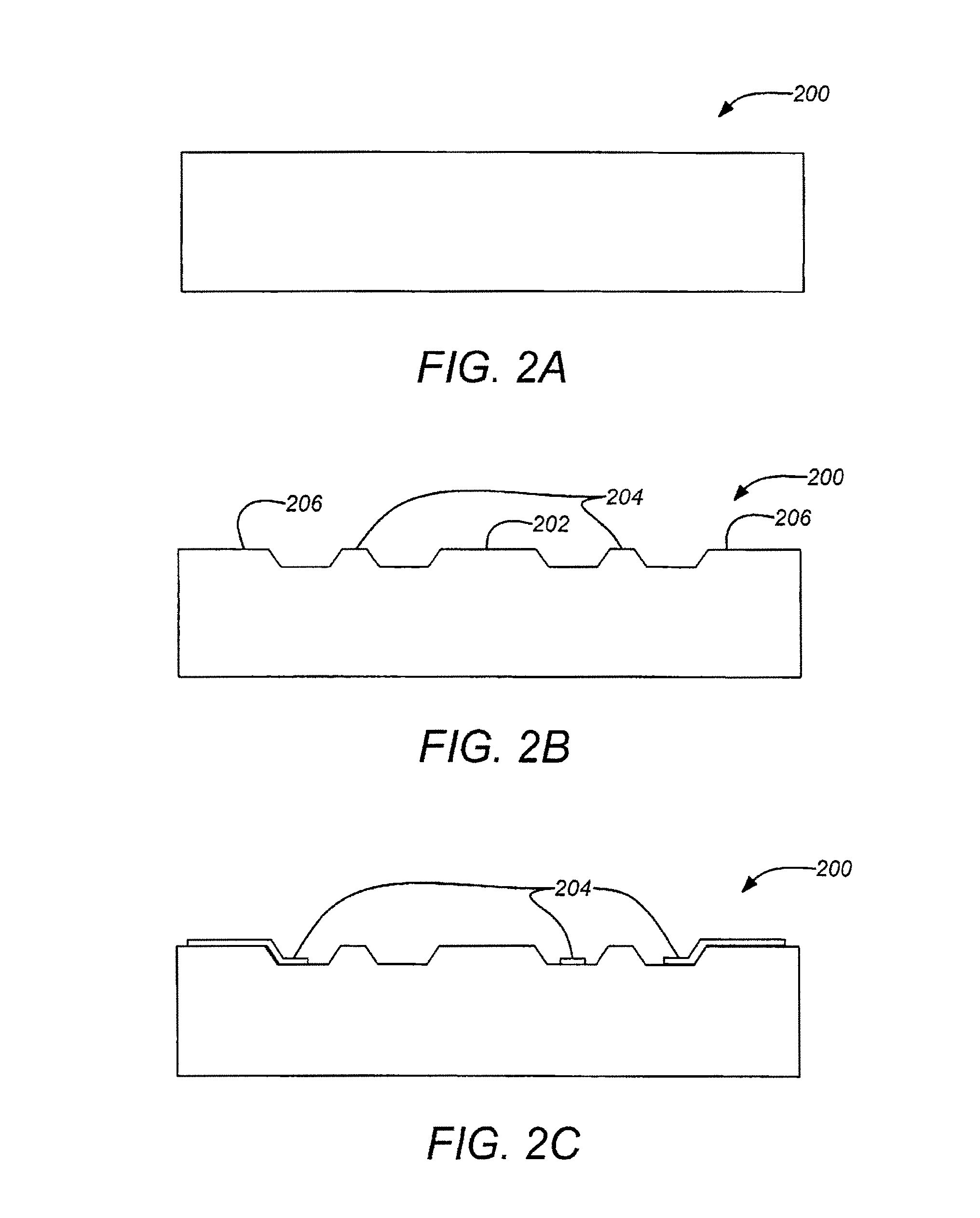
FIGS. 2A-2F illustrate a manufacturing process of a complete baseplate wafer for use in an all-quartz resonator gyroscope in sequence. The quartz baseplate wafer fabrication begins with a recess etch of the fused quartz wafer 200 as shown in FIG. 2B using either a fluorine-chemistry plasma or hydrofluoric acid process or any other known process capable of etching quartz to yield the appropriate pattern (e.g. matching the planar resonator layout of FIG. 1A) of recesses leaving high spots for the central support location 202 of the planar resonator and to provide contacts for the electrode locations 204 as well as the DRG case wall location 206 (for the cap wafer detailed hereafter). The etched recesses provide areas in which electrical circuit interconnects can be deposited to appropriately connect the drive and sense electrodes to the control circuitry. Following the etching, Ti/Au or Cr/Au (200 A/5000 A) are metallized on the wafer 200 to form the interconnects 208 for the electrodes as shown in FIG. 2C. A plasma enhanced chemical vapor deposition (PECVD) silicon dioxide or silicon nitride (5000 .ANG.) is then deposited to form the inter-metal dielectric layer 210 as shown in FIG. 2D. Reactive ion etching (RIE) may then be used to open vias 212 through the inter-metal dielectric layer 210 as shown in FIG. 2E. A second metallization of Ti/Au or Cr/Au (200 .ANG./5000 .ANG.) may be used to deposit the metal bond pads 214 and a vacuum seal ring 216 as shown in FIG. 2F. This concludes the baseplate wafer 200 fabrication.
FIG. 2G is a flowchart of an exemplary method 220 of manufacturing a baseplate wafer for an all-quartz resonator gyroscope. In operation 222, a first fused quartz wafer is provided for a baseplate as shown in FIG. 2A. In operation 224, recesses are etched in the fused quartz baseplate as shown in FIG. 2B. In operation 226, metal interconnects are deposited on the fused quartz baseplate as shown in FIG. 2C. In operation 228, dielectric film is deposited over the interconnects as shown in FIG. 2D. In operation 230, vias are etched in the dielectric film as shown in FIG. 2E. And in operation 232, bond metal and a seal ring are deposited as shown in FIG. 2F. The seal ring marks out the periphery of the disc resonator and the bond metal is used to mount the disc resonator at the central support and the electrodes throughout the interior of the disc.
FIGS. 3A-3G illustrate a manufacturing process of a resonator wafer for an all-quartz resonator gyroscope, in sequence. The starting materials for the resonator wafer process are a full fused quartz resonator wafer 300 (FIG. 3A) and another fused quartz wafer to be used as a handle wafer 302 (FIG. 3B) having release holes 304 (which may be ultrasonically machined through it). A silicon thin film 306 (approximately 1 .mu.m) is deposited on the resonator wafer 300 using a plasma enhanced chemical vapor deposition (PECVD) as shown in FIG. 3C or using SOI technology as will be understood by those skilled in the art. A chemical mechanical planarization (CMP) step may be carried out if there are any unacceptable surface imperfections due to the deposition. The silicon film may then be patterned 308 using a fluorine chemistry RIE as shown in FIG. 3D in regions that are not required for later bonding the etched resonator to the baseplate wafer. This will speed the final release step. In general, depending upon the applied resonator architecture the pattern will provide enough bonding area in the appropriate locations so that the resonator wafer 300 is stable on the handle wafer 302, but allowing relatively easy release of the handle wafer 302 in later processing. The resonator wafer 300 with patterned silicon film 308 is then bonded to the handle wafer 302 with through holes as shown in FIG. 3E.
FIG. 3F illustrates an optional process of additional etching of the bottom of the disc resonator wafer 300 as shown. This may be done to form raised areas for the central support location 310 and electrode locations 312 where the baseplate wafer 200 will be bonded in subsequent processing.
FIG. 3G then illustrates deep reactive ion etching (DRIE) that may be used to define the resonator pattern (e.g. the pattern shown in FIG. 1A) including the electrodes and central support with straight side walls 314 completely through the resonator wafer 300. DRIE of fused quartz defines resonator with straight side walls and minimal surface roughness. Note that the electrodes are now embedded within the resonator wafer 300 but physically disconnected from the resonator structure. Thus, the handle wafer 302 now supports the pattern of resonator structure and electrodes in the resonator wafer 300.
The bonding surface of the resonator and the sidewalls are then metallized 316 with either the bilayer High Q coating or the alternate metal High Q coating, each discussed above. Both provide highly conformal and highly uniform coatings on the atomic scale. Thus, the thickness of a conductive coating can be reduced to a minimum while maintaining a continuous coating in high aspect ratio structures, including those having an aspect ratio in excess of 5:1. For example, FIG. 8 is a scanning electron microscope image 800 of the etched disc resonator wafer 300 having a 30 nm thick platinum coating formed directly thereon in accordance with the alternate metal High Q method described above.
FIG. 3I is a flowchart of a method 320 of manufacturing a resonator wafer for an all-quartz resonator gyroscope, including the bilayer High Q coating. In operation 322, a second fused quartz wafer is received for the disc resonator as shown in FIG. 3A. In operation 324, a third fused quartz wafer is received for a handle with ultrasonically machined or laser machined through holes as shown in FIG. 3B. In operation 326, amorphous silicon thin film is deposited on the second wafer with chemical mechanical planarization (CMP) performed as necessary as shown in FIG. 3C. In operation 328, silicon is patterned on the second wafer as shown in FIG. 3D. In operation 330, the second wafer is bonded to the third wafer as shown in FIG. 3E. The wafers may be bonded with plasma-assisted room temperature bonding. Though not shown in FIG. 31, an optional process of additional etching of the bottom of the disc resonator wafer for electrode and support contacts as shown in FIG. 3F, can be performed subsequent to operation 330 and before operation 332.
In operation 332, the second wafer is deep reactive ion etched (DRIE) to define the disc resonator with straight side walls as shown in FIG. 3G. The sidewalls define gaps 101 between rings 103 or drive/sensor electrodes 104/106 with a height-to-width aspect ratio between 3:1 and 10:1. In operation 334, an Al.sub.2O.sub.3 amorphous film is deposited on the etched quartz resonator wafer by Atomic Layer Deposition, as discussed above and shown in FIG. 7, to form the first layer of the bilayer High Q coating on the bonding surface and sidewalls of the disc resonator. Preferably, the deposited Al.sub.2O.sub.3 amorphous film is 1 to 2 nm-thick. In operation 336, a noble metal film is deposited on the Al.sub.2O.sub.3 amorphous film, also as discussed above and shown in FIG. 7, to form the second layer of the bilayer High Q coating on the bonding surface and sidewalls of the disc resonator. Preferably, the deposited noble metal film is 1 to 20 nm thick. Together, the ALD Al.sub.2O.sub.3 amorphous film and the ALD metal film form a bilayer High Q coating that is ultra-thin, highly conformal, and highly conductive, as discussed above.
FIGS. 4A-4B illustrate assembly of a resonator wafer and baseplate wafer for an all-quartz resonator gyroscope. The resonator wafer 300 and handle wafer 302 pair are then brought in contact and aligned with the baseplate wafer 200. The resonator wafer 300 and baseplate wafer 200 may be bonded together using a metal/metal thermal compression bond, to bond the metal bond pads 214 of the baseplate wafer 200 to the central support location 310 and the electrode locations 312 of the resonator wafer 300 as shown in FIG. 4A. Alignment can be performed through the transparent baseplate wafer for .about 0.5 .mu.m accuracy. These bonds form the electrical connections to the electrodes and resonator structure. To release the resonator structure from the handle wafer, Xenon Difluoride gas (shown by arrows in FIG. 4B) may be passed through the release holes of the handle wafer to undercut the silicon layer complete the transfer of the resonator wafer 300 from the handle wafer 302 to the baseplate 200. The top side of the resonator wafer may then be coated with thin metallic layer 400 (e.g., approximately 10-20 nm thick) Al or Au with angled evaporation to form a completely symmetric structure and prevent shorting of probe pads.
The final structure is illustrated in FIG. 4C.
FIG. 4D is a flowchart of a method 420 of assembling a resonator wafer and baseplate wafer for an all-quartz resonator gyroscope. In operation 422, the second and the third wafer pair are bonded to the first wafer with metal-to-metal thermal compression bonding as shown in FIG. 4A. Alignment of the second and third wafers may be performed through the transparent first wafer to achieve about 0.5 .mu.m accuracy. In operation 424, the third wafer is removed from the second wafer by undercutting the silicon layer using Xenon Difluoride dry release as shown in FIG. 4B. The flow of Xenon Difluoride is indicated by the arrows. And in operation 426, the top side of the second wafer is metallized with angled deposition through a shadow mask to prevent shorting of probe pads as shown in FIG. 4C. Thus, the disc resonator is symmetrically coated with a thin conductive layer of metal to allow it to function electrostatically with the electrodes.
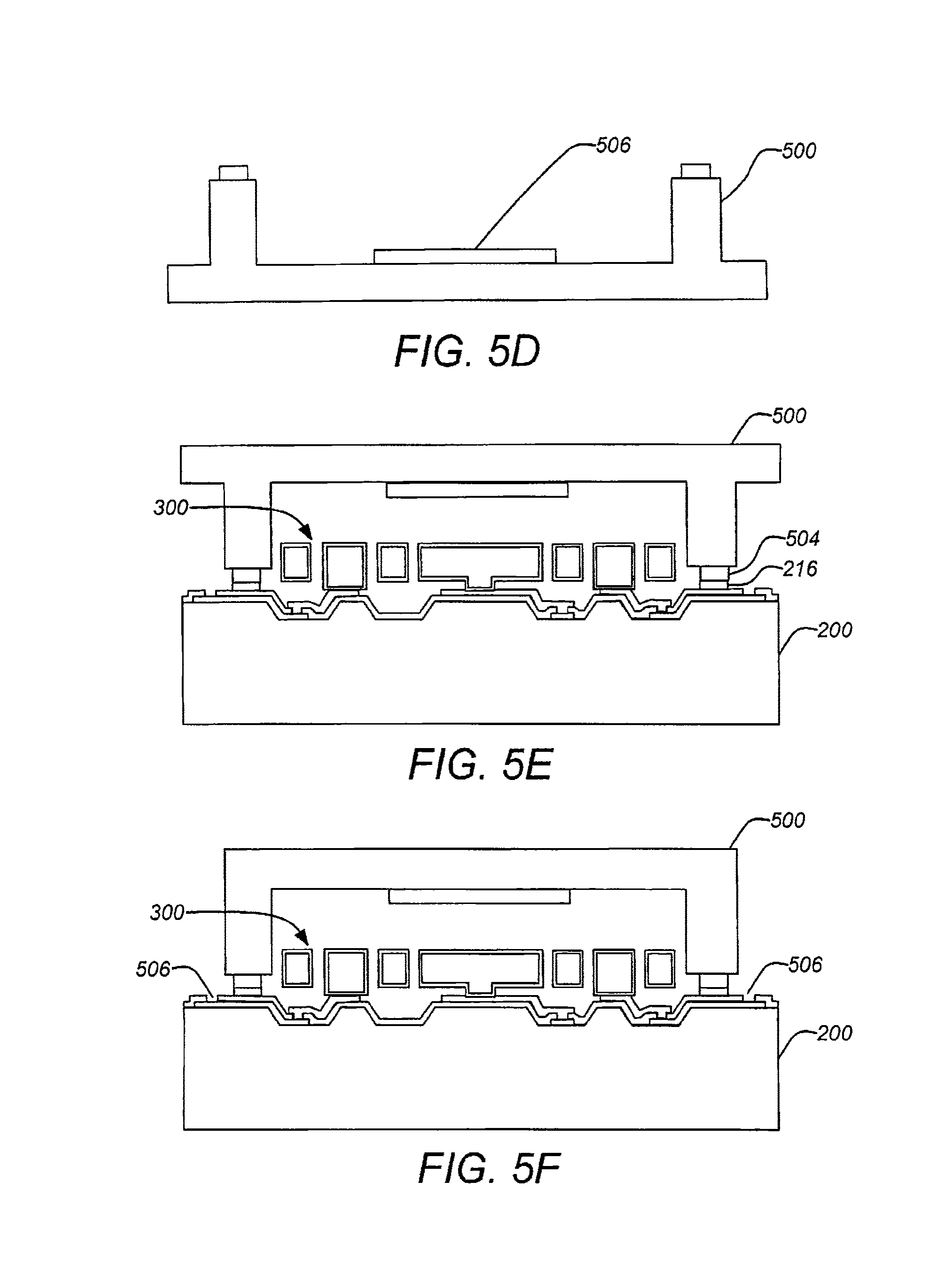
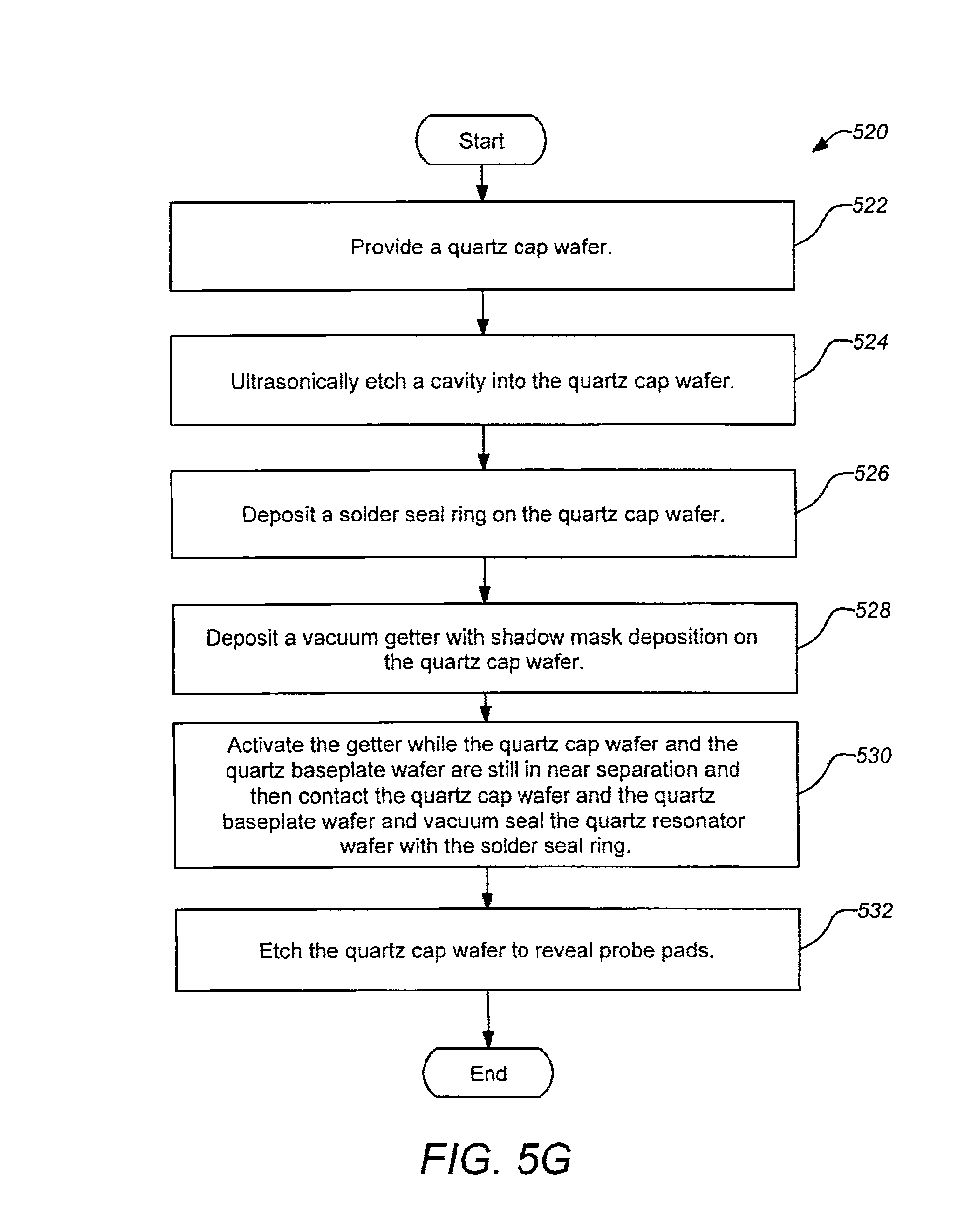
FIGS. 5A-5F illustrate a vacuum sealing process of a resonator wafer 300 and baseplate wafer 200 for an all-quartz resonator gyroscope. The vacuum sealing process begins with a cavity 502 etched into a fused quartz cap wafer 500, e.g. using ultrasonic machining as shown in FIG. 5B. Then indium or tin solder (.about.5 .mu.m thick) may be deposited using spray coating lithograph) and lift-off to form a metal bond line 504 around the perimeter of the cavity 502 as shown in FIG. 5C. A vacuum getter 506 may then be deposited into the cavity using a shadow mask as shown in FIG. 5D. For example the vacuum getter may comprise a titanium-based thin film getter or any similar getter material compatible with the structure and processes defined herein. The cap wafer 500 is brought to the resonator wafer 300 and baseplate wafer 200 pair and aligned using a bond aligner known in the art. For example, a bond aligner system from Electronic Vision Group or other similar systems may be applied to properly bond the wafers previously aligned to one another. The cap wafer 500 may be temporarily kept in near separation from the resonator wafer 300 and baseplate wafer 200 pair with 50 .mu.m thick spacers. This three-wafer stack is then transferred to a wafer bonder so that the cavity of the cap wafer 500 can be evacuated through the gap created by the 50 .mu.m-thick spacers. Once vacuum is achieved inside the cavity, the vacuum getter may be heated to approximately 350.degree. C. for activation. The 50 .mu.m thick spacers may then be removed to contact the metal bond line 504 of the cap wafer 500 to the vacuum seal ring 216 of the baseplate wafer 200 to form the vacuum seal with the solder as shown in FIG. 5E. Note that the electrical interconnects to the resonator and electrodes pass under the vacuum seal. Finally, the cap wafer 500 may be ultrasonically machined to create access to the probe pads to the electrical interconnects of the gyroscope as shown in FIG. 5F.
FIG. 5G is a flowchart of a vacuum sealing method 520 of a resonator wafer and baseplate wafer for an all-quartz resonator gyroscope. In operation 522, a fourth fused quartz wafer is provided for a cap wafer as shown in FIG. 5A. In operation 524, a cavity is ultrasonically etched into the cap wafer as shown in FIG. 5B. In operation 526, a solder seal ring is deposited with spray coating lithography and lifted-off as shown in FIG. 5C. In operation 528, a vacuum getter is deposited with shadow mask deposition as shown in FIG. 50. In operation 530, the getter is activated while the cap wafer and the baseplate wafer are still separated and then the cap wafer and the baseplate wafer are contacted to vacuum seal the resonator wafer with the solder seal ring as shown in FIG. 5E. And in operation 532, the cap wafer is then etched to reveal probe pads as shown in FIG. 5F.
FIGS. 6A and 6B illustrate an embodiment of an all-quartz resonator gyroscope 610 including integral control electronics. In general, the gyroscope 610 is developed as described above with some additional processing. In FIG. 6A the all-quartz disc resonator gyroscope is vacuum sealed (consistent with the process outlined in FIGS. 5A-5G) with through wafer interconnects 600 and backside indium bond pads 602 integrated into the baseplate wafer 604. The baseplate wafer 604 may be produced just as the baseplate wafer 200 of FIGS. 2A-2G with the addition of the through wafer interconnects 600 being integrated into the baseplate wafer 604 prior to the metallization patterning on the wafer to form the interconnects for the electrodes as shown in FIG. 2C. In this case, the metallization is connected to the through wafer interconnects 600. Further metallization may be patterned on the backside of the baseplate wafer 604 from the through wafer interconnects 600 to the bond pads 602. In FIG. 6B control electronics 606 (e.g. an ASIC control electronics chip) may be flip-chip bonded to the all-quartz disc resonator gyroscope package with electrical connections going directly from the electronics to the electrodes and resonator within the vacuum sealed package.
This concludes the description including preferred embodiments of the present invention. The foregoing description including preferred embodiments of the invention has been presented for the purposes of illustration and description. It is not intended to be exhaustive or to limit the invention to the precise forms disclosed. Many modifications and variations are possible within the scope of the foregoing teachings. Additional variations of the present invention may be devised without departing from the inventive concept as set forth in the following claims.
* * * * *
References
D00000
D00001
D00002
D00003
D00004
D00005
D00006
D00007
D00008
D00009
D00010
D00011
D00012

D00013

D00014

D00015
D00016
D00017

D00018

D00019

XML
uspto.report is an independent third-party trademark research tool that is not affiliated, endorsed, or sponsored by the United States Patent and Trademark Office (USPTO) or any other governmental organization. The information provided by uspto.report is based on publicly available data at the time of writing and is intended for informational purposes only.
While we strive to provide accurate and up-to-date information, we do not guarantee the accuracy, completeness, reliability, or suitability of the information displayed on this site. The use of this site is at your own risk. Any reliance you place on such information is therefore strictly at your own risk.
All official trademark data, including owner information, should be verified by visiting the official USPTO website at www.uspto.gov. This site is not intended to replace professional legal advice and should not be used as a substitute for consulting with a legal professional who is knowledgeable about trademark law.