Programmable code generation for radar sensing systems
Maher , et al. March 2, 2
U.S. patent number 10,935,633 [Application Number 16/884,155] was granted by the patent office on 2021-03-02 for programmable code generation for radar sensing systems. This patent grant is currently assigned to Uhnder, Inc.. The grantee listed for this patent is UHNDER, INC.. Invention is credited to Murtaza Ali, Jean Pierre Bordes, Steve Borho, Curtis Davis, Srikanth Gollapudi, Monier Maher, Raghunath Krishna Rao, Frederick Rush, Wayne E. Stark.


View All Diagrams
| United States Patent | 10,935,633 |
| Maher , et al. | March 2, 2021 |
Programmable code generation for radar sensing systems
Abstract
A radar sensing system for a vehicle has multiple transmitters and receivers on a vehicle. The transmitters are configured to transmit radio signals which are reflected off of objects in the environment. There are one or more receivers that receive the reflected radio signals. Each receiver has an antenna, a radio frequency front end, an analog-to-digital converter (ADC), and a digital signal processor. The transmitted signals are based on spreading codes generated by a programmable code generation unit. The receiver also makes use of the spreading codes generated by the programmable code generation unit. The programmable code generation unit is configured to selectively generate particular spreading codes that have desired properties.
| Inventors: | Maher; Monier (St. Louis, MO), Bordes; Jean Pierre (St. Charles, MO), Stark; Wayne E. (Ann Arbor, MI), Rao; Raghunath Krishna (Austin, TX), Rush; Frederick (Austin, TX), Davis; Curtis (St. Louis, MO), Gollapudi; Srikanth (Austin, TX), Borho; Steve (St. Charles, MO), Ali; Murtaza (Cedar Park, TX) | ||||||||||
|---|---|---|---|---|---|---|---|---|---|---|---|
| Applicant: |
|
||||||||||
| Assignee: | Uhnder, Inc. (Austin,
TX) |
||||||||||
| Family ID: | 1000005394259 | ||||||||||
| Appl. No.: | 16/884,155 | ||||||||||
| Filed: | May 27, 2020 |
Prior Publication Data
| Document Identifier | Publication Date | |
|---|---|---|
| US 20200284873 A1 | Sep 10, 2020 | |
Related U.S. Patent Documents
| Application Number | Filing Date | Patent Number | Issue Date | ||
|---|---|---|---|---|---|
| 15892865 | Feb 9, 2018 | 10670695 | |||
| 62457394 | Feb 10, 2017 | ||||
| Current U.S. Class: | 1/1 |
| Current CPC Class: | G01S 13/64 (20130101); G01S 13/584 (20130101); G11C 11/409 (20130101); G01S 13/931 (20130101); G01S 7/352 (20130101); G01S 13/87 (20130101); G01S 13/06 (20130101); G01S 7/032 (20130101); G01S 13/42 (20130101); G01S 7/354 (20130101); G01S 13/325 (20130101); G01S 7/4021 (20130101); G01S 2013/93271 (20200101); G01S 2013/93272 (20200101); G01S 7/285 (20130101); G01S 7/4017 (20130101); G01S 2013/93274 (20200101); G06F 7/724 (20130101); G01S 13/34 (20130101); G01S 13/878 (20130101) |
| Current International Class: | G01S 7/35 (20060101); G01S 13/64 (20060101); G01S 7/03 (20060101); G01S 13/87 (20060101); G01S 13/42 (20060101); G01S 13/58 (20060101); G11C 11/409 (20060101); G01S 7/285 (20060101); G01S 7/40 (20060101); G01S 13/32 (20060101); G01S 13/34 (20060101); G01S 13/931 (20200101); G01S 13/06 (20060101); G06F 7/72 (20060101) |
References Cited [Referenced By]
U.S. Patent Documents
| 1882128 | October 1932 | Fearing |
| 3374478 | March 1968 | Blau |
| 3735398 | May 1973 | Ross |
| 3750169 | July 1973 | Strenglein |
| 3766554 | October 1973 | Tresselt |
| 3896434 | July 1975 | Sirven |
| 3932871 | January 1976 | Foote |
| 4078234 | March 1978 | Fishbein et al. |
| 4176351 | November 1979 | De Vita et al. |
| 4308536 | December 1981 | Sims, Jr. et al. |
| 4566010 | January 1986 | Collins |
| 4612547 | September 1986 | Itoh |
| 4882668 | November 1989 | Schmid et al. |
| 4910464 | March 1990 | Trett et al. |
| 4939685 | July 1990 | Feintuch |
| 5001486 | March 1991 | Bachtiger |
| 5012254 | April 1991 | Thompson |
| 5034906 | July 1991 | Chang |
| 5087918 | February 1992 | May et al. |
| 5151702 | September 1992 | Urkowitz |
| 5175710 | December 1992 | Hutson |
| 5218619 | June 1993 | Dent |
| 5272663 | December 1993 | Jones et al. |
| 5280288 | January 1994 | Sherry et al. |
| 5302956 | April 1994 | Asbury et al. |
| 5341141 | August 1994 | Frazier et al. |
| 5345470 | September 1994 | Alexander |
| 5361072 | November 1994 | Barrick et al. |
| 5376939 | December 1994 | Urkowitz |
| 5379322 | January 1995 | Kosaka et al. |
| 5497162 | March 1996 | Kaiser |
| 5508706 | April 1996 | Tsou et al. |
| 5581464 | December 1996 | Woll et al. |
| 5654715 | August 1997 | Hayashikura et al. |
| 5657021 | August 1997 | Ehsani-Nategh et al. |
| 5657023 | August 1997 | Lewis et al. |
| 5691724 | November 1997 | Aker et al. |
| 5712640 | January 1998 | Andou |
| 5724041 | March 1998 | Inoue et al. |
| 5847661 | December 1998 | Ricci |
| 5892477 | April 1999 | Wehling |
| 5917430 | June 1999 | Greneker, III et al. |
| 5920285 | July 1999 | Benjamin |
| 5931893 | August 1999 | Dent et al. |
| 5959571 | September 1999 | Aoyagi et al. |
| 5970400 | October 1999 | Dwyer |
| 6048315 | April 2000 | Chiao et al. |
| 6067314 | May 2000 | Azuma |
| 6069581 | May 2000 | Bell et al. |
| 6121872 | September 2000 | Weishaupt |
| 6121918 | September 2000 | Tullsson |
| 6151366 | November 2000 | Yip |
| 6163252 | December 2000 | Nishiwaki |
| 6184829 | February 2001 | Stilp |
| 6191726 | February 2001 | Tullsson |
| 6208248 | March 2001 | Ross |
| 6288672 | September 2001 | Asano et al. |
| 6307622 | October 2001 | Lewis |
| 6335700 | January 2002 | Ashihara |
| 6347264 | February 2002 | Nicosia et al. |
| 6400308 | June 2002 | Bell et al. |
| 6411250 | June 2002 | Oswald et al. |
| 6417796 | July 2002 | Bowlds |
| 6424289 | July 2002 | Fukae et al. |
| 6547733 | April 2003 | Hwang et al. |
| 6583753 | June 2003 | Reed |
| 6614387 | September 2003 | Deadman |
| 6624784 | September 2003 | Yamaguchi |
| 6674908 | January 2004 | Aronov |
| 6683560 | January 2004 | Bauhahn |
| 6714956 | March 2004 | Liu et al. |
| 6747595 | June 2004 | Hirabe |
| 6768391 | July 2004 | Dent et al. |
| 6865218 | March 2005 | Sourour |
| 6888491 | May 2005 | Richter |
| 6975246 | December 2005 | Trudeau |
| 7066886 | June 2006 | Song |
| 7119739 | October 2006 | Struckman |
| 7130663 | October 2006 | Guo |
| 7202776 | April 2007 | Breed |
| 7289058 | October 2007 | Shima |
| 7299251 | November 2007 | Skidmore et al. |
| 7338450 | March 2008 | Kristofferson et al. |
| 7395084 | July 2008 | Anttila |
| 7460055 | December 2008 | Nishijima et al. |
| 7474258 | January 2009 | Arikan et al. |
| 7545310 | June 2009 | Matsuoka |
| 7545321 | June 2009 | Kawasaki |
| 7564400 | July 2009 | Fukuda |
| 7567204 | July 2009 | Sakamoto |
| 7609198 | October 2009 | Chang |
| 7642952 | January 2010 | Fukuda |
| 7663533 | February 2010 | Toennesen |
| 7667637 | February 2010 | Pedersen et al. |
| 7728762 | June 2010 | Sakamoto |
| 7791528 | September 2010 | Klotzbuecher |
| 7847731 | December 2010 | Wiesbeck et al. |
| 7855677 | December 2010 | Negoro et al. |
| 7859450 | December 2010 | Shirakawa et al. |
| 8019352 | September 2011 | Rappaport et al. |
| 8044845 | October 2011 | Saunders |
| 8049663 | November 2011 | Frank et al. |
| 8059026 | November 2011 | Nunez |
| 8102306 | January 2012 | Smith, Jr. et al. |
| 8115672 | February 2012 | Nouvel et al. |
| 8154436 | April 2012 | Szajnowski |
| 8169359 | May 2012 | Aoyagi |
| 8212713 | July 2012 | Aiga et al. |
| 8330650 | December 2012 | Goldman |
| 8390507 | March 2013 | Wintermantel |
| 8471760 | June 2013 | Szajnowski |
| 8532159 | September 2013 | Kagawa et al. |
| 8547988 | October 2013 | Hadani et al. |
| 8686894 | April 2014 | Fukuda et al. |
| 8694306 | April 2014 | Short et al. |
| 8994581 | March 2015 | Brown |
| 9121943 | September 2015 | Stirlin-Gallacher et al. |
| 9239378 | January 2016 | Kishigami et al. |
| 9239379 | January 2016 | Burgio et al. |
| 9274217 | March 2016 | Chang et al. |
| 9282945 | March 2016 | Smith et al. |
| 9335402 | May 2016 | Maeno et al. |
| 9400328 | July 2016 | Hsiao et al. |
| 9541639 | January 2017 | Searcy et al. |
| 9568600 | February 2017 | Alland |
| 9575160 | February 2017 | Davis et al. |
| 9599702 | March 2017 | Bordes et al. |
| 9689967 | June 2017 | Stark et al. |
| 9720073 | August 2017 | Davis et al. |
| 9720080 | September 2017 | Rodenbeck |
| 9753121 | September 2017 | Davis |
| 9753132 | September 2017 | Bordes et al. |
| 9772397 | September 2017 | Bordes et al. |
| 9791551 | October 2017 | Eshraghi et al. |
| 9791564 | October 2017 | Harris et al. |
| 9806914 | October 2017 | Bordes et al. |
| 9829567 | November 2017 | Davis et al. |
| 9846228 | December 2017 | Davis et al. |
| 9869762 | January 2018 | Alland et al. |
| 1009219 | October 2018 | Lashkari et al. |
| 2001/0002919 | June 2001 | Sourour et al. |
| 2002/0004692 | January 2002 | Nicosia et al. |
| 2002/0044082 | April 2002 | Woodington et al. |
| 2002/0075178 | June 2002 | Woodington et al. |
| 2002/0118522 | August 2002 | Ho et al. |
| 2002/0130811 | September 2002 | Voigtlaender |
| 2002/0147534 | October 2002 | Delcheccolo et al. |
| 2002/0155811 | October 2002 | Prismantas |
| 2003/0001772 | January 2003 | Woodington et al. |
| 2003/0011519 | January 2003 | Breglia et al. |
| 2003/0058166 | March 2003 | Hirabe |
| 2003/0073463 | April 2003 | Shapira |
| 2003/0080713 | May 2003 | Kirmuss |
| 2003/0102997 | June 2003 | Levin et al. |
| 2003/0235244 | December 2003 | Pessoa et al. |
| 2004/0012516 | January 2004 | Schiffmann |
| 2004/0015529 | January 2004 | Tanrikulu et al. |
| 2004/0066323 | April 2004 | Richter |
| 2004/0070532 | April 2004 | Ishii et al. |
| 2004/0107030 | June 2004 | Nishira et al. |
| 2004/0138802 | July 2004 | Kuragaki et al. |
| 2004/0215373 | October 2004 | Won et al. |
| 2005/0008065 | January 2005 | Schilling |
| 2005/0069162 | March 2005 | Haykin |
| 2005/0090274 | April 2005 | Miyashita |
| 2005/0156780 | July 2005 | Bonthron |
| 2005/0201457 | September 2005 | Allred et al. |
| 2005/0225476 | October 2005 | Hoetzel et al. |
| 2005/0273480 | December 2005 | Pugh et al. |
| 2006/0012511 | January 2006 | Dooi et al. |
| 2006/0036353 | February 2006 | Wintermantel |
| 2006/0050707 | March 2006 | Sterin |
| 2006/0093078 | May 2006 | Lewis et al. |
| 2006/0109170 | May 2006 | Voigtlaender et al. |
| 2006/0109931 | May 2006 | Asai |
| 2006/0114324 | June 2006 | Farmer et al. |
| 2006/0140249 | June 2006 | Kohno |
| 2006/0181448 | August 2006 | Natsume et al. |
| 2006/0220943 | October 2006 | Schlick et al. |
| 2006/0244653 | November 2006 | Szajnowski |
| 2006/0262007 | November 2006 | Bonthron |
| 2006/0262009 | November 2006 | Watanabe |
| 2007/0018884 | January 2007 | Adams |
| 2007/0018886 | January 2007 | Watanabe et al. |
| 2007/0096885 | May 2007 | Cheng et al. |
| 2007/0109175 | May 2007 | Fukuda |
| 2007/0115869 | May 2007 | Lakkis |
| 2007/0120731 | May 2007 | Kelly, Jr. et al. |
| 2007/0132633 | June 2007 | Uchino |
| 2007/0152870 | July 2007 | Woodington et al. |
| 2007/0152871 | July 2007 | Puglia |
| 2007/0152872 | July 2007 | Woodington |
| 2007/0164896 | July 2007 | Suzuki et al. |
| 2007/0171122 | July 2007 | Nakano |
| 2007/0182619 | August 2007 | Honda et al. |
| 2007/0182623 | August 2007 | Zeng |
| 2007/0188373 | August 2007 | Shirakawa et al. |
| 2007/0200747 | August 2007 | Okai |
| 2007/0263748 | November 2007 | Mesecher |
| 2007/0279303 | December 2007 | Schoebel |
| 2008/0088499 | April 2008 | Bonthron |
| 2008/0094274 | April 2008 | Nakanishi |
| 2008/0150790 | June 2008 | Voigtlaender et al. |
| 2008/0180311 | July 2008 | Mikami |
| 2008/0208472 | August 2008 | Morcom |
| 2008/0218406 | September 2008 | Nakanishi |
| 2008/0258964 | October 2008 | Schoeberl |
| 2008/0272955 | November 2008 | Yonak et al. |
| 2009/0003412 | January 2009 | Negoro et al. |
| 2009/0015459 | January 2009 | Mahler et al. |
| 2009/0015464 | January 2009 | Fukuda |
| 2009/0027257 | January 2009 | Arikan |
| 2009/0046000 | February 2009 | Matsuoka |
| 2009/0051581 | February 2009 | Hatono |
| 2009/0072957 | March 2009 | Wu et al. |
| 2009/0073025 | March 2009 | Inoue |
| 2009/0074031 | March 2009 | Fukuda |
| 2009/0079617 | March 2009 | Shirakawa et al. |
| 2009/0085827 | April 2009 | Orime et al. |
| 2009/0103593 | April 2009 | Bergamo |
| 2009/0121918 | May 2009 | Shirai et al. |
| 2009/0212998 | August 2009 | Szajnowski |
| 2009/0237293 | September 2009 | Sakuma |
| 2009/0254260 | October 2009 | Nix et al. |
| 2009/0267822 | October 2009 | Shinoda et al. |
| 2009/0289831 | November 2009 | Akita |
| 2009/0295623 | December 2009 | Falk |
| 2010/0001897 | January 2010 | Lyman |
| 2010/0019950 | January 2010 | Yamano et al. |
| 2010/0039311 | February 2010 | Woodington et al. |
| 2010/0116365 | May 2010 | McCarty |
| 2010/0156690 | June 2010 | Kim et al. |
| 2010/0198513 | August 2010 | Zeng et al. |
| 2010/0253573 | October 2010 | Holzheimer et al. |
| 2010/0277359 | November 2010 | Ando |
| 2010/0289692 | November 2010 | Winkler |
| 2011/0006944 | January 2011 | Goldman |
| 2011/0032138 | February 2011 | Krapf |
| 2011/0074620 | March 2011 | Wintermantel |
| 2011/0187600 | August 2011 | Landt |
| 2011/0196568 | August 2011 | Nickolaou |
| 2011/0234448 | September 2011 | Hayase |
| 2011/0248796 | October 2011 | Pozgay |
| 2011/0279303 | November 2011 | Smith, Jr. et al. |
| 2011/0279307 | November 2011 | Song |
| 2011/0285576 | November 2011 | Lynam |
| 2011/0291874 | December 2011 | De Mersseman |
| 2011/0291875 | December 2011 | Szajnowski |
| 2011/0292971 | December 2011 | Hadani et al. |
| 2011/0298653 | December 2011 | Mizutani |
| 2012/0001791 | January 2012 | Wintermantel |
| 2012/0050093 | March 2012 | Heilmann et al. |
| 2012/0105268 | May 2012 | Smits et al. |
| 2012/0112957 | May 2012 | Nguyen et al. |
| 2012/0133547 | May 2012 | MacDonald et al. |
| 2012/0173246 | July 2012 | Choi et al. |
| 2012/0195349 | August 2012 | Lakkis |
| 2012/0249356 | October 2012 | Shope |
| 2012/0257643 | October 2012 | Wu et al. |
| 2012/0314799 | December 2012 | In De Betou et al. |
| 2012/0319900 | December 2012 | Johansson et al. |
| 2013/0016761 | January 2013 | Nentwig |
| 2013/0021196 | January 2013 | Himmelstoss |
| 2013/0027240 | January 2013 | Chowdhury |
| 2013/0057436 | March 2013 | Krasner et al. |
| 2013/0069818 | March 2013 | Shirakawa et al. |
| 2013/0102254 | April 2013 | Cyzs |
| 2013/0113647 | May 2013 | Sentelle et al. |
| 2013/0113652 | May 2013 | Smits et al. |
| 2013/0113653 | May 2013 | Kishigami et al. |
| 2013/0135140 | May 2013 | Kishigami |
| 2013/0169468 | July 2013 | Johnson et al. |
| 2013/0169485 | July 2013 | Lynch |
| 2013/0176154 | July 2013 | Bonaccio et al. |
| 2013/0214961 | August 2013 | Lee et al. |
| 2013/0229301 | September 2013 | Kanamoto |
| 2013/0244710 | September 2013 | Nguyen et al. |
| 2013/0249730 | September 2013 | Adcook |
| 2013/0314271 | November 2013 | Braswell et al. |
| 2013/0321196 | December 2013 | Binzer et al. |
| 2014/0022108 | January 2014 | Alberth, Jr. et al. |
| 2014/0028491 | January 2014 | Ferguson |
| 2014/0035774 | February 2014 | Khlifi |
| 2014/0070985 | March 2014 | Vacanti |
| 2014/0085128 | March 2014 | Kishigami |
| 2014/0097987 | April 2014 | Worl et al. |
| 2014/0111367 | April 2014 | Kishigami et al. |
| 2014/0111372 | April 2014 | Wu |
| 2014/0139322 | May 2014 | Wang et al. |
| 2014/0159948 | June 2014 | Ishimori et al. |
| 2014/0220903 | August 2014 | Schulz et al. |
| 2014/0253345 | September 2014 | Breed |
| 2014/0253364 | September 2014 | Lee et al. |
| 2014/0285373 | September 2014 | Kuwahara et al. |
| 2014/0316261 | October 2014 | Lux et al. |
| 2014/0327566 | November 2014 | Burgio et al. |
| 2014/0340254 | November 2014 | Hesse |
| 2014/0348253 | November 2014 | Mobasher et al. |
| 2015/0002329 | January 2015 | Murad et al. |
| 2015/0002357 | January 2015 | Sanford et al. |
| 2015/0035662 | February 2015 | Bowers et al. |
| 2015/0061922 | March 2015 | Kishigami |
| 2015/0103745 | April 2015 | Negus et al. |
| 2015/0198709 | July 2015 | Inoue |
| 2015/0204966 | July 2015 | Kishigami |
| 2015/0204971 | July 2015 | Yoshimura et al. |
| 2015/0204972 | July 2015 | Kuehnle et al. |
| 2015/0226848 | August 2015 | Park |
| 2015/0234045 | August 2015 | Rosenblum |
| 2015/0247924 | September 2015 | Kishigami |
| 2015/0255867 | September 2015 | Inoue |
| 2015/0301172 | October 2015 | Ossowska |
| 2015/0323660 | November 2015 | Hampikian |
| 2015/0331090 | November 2015 | Jeong et al. |
| 2015/0369912 | December 2015 | Kishigami et al. |
| 2016/0003938 | January 2016 | Gazit et al. |
| 2016/0003939 | January 2016 | Stainvas Olshansky et al. |
| 2016/0018511 | January 2016 | Nayyar et al. |
| 2016/0033631 | February 2016 | Searcy et al. |
| 2016/0033632 | February 2016 | Searcy et al. |
| 2016/0041260 | February 2016 | Cao et al. |
| 2016/0054441 | February 2016 | Kuo et al. |
| 2016/0061935 | March 2016 | McCloskey et al. |
| 2016/0084941 | March 2016 | Arage |
| 2016/0084943 | March 2016 | Arage |
| 2016/0091595 | March 2016 | Alcalde |
| 2016/0103206 | April 2016 | Pavao-Moreira et al. |
| 2016/0124075 | May 2016 | Vogt et al. |
| 2016/0124086 | May 2016 | Jansen et al. |
| 2016/0131752 | May 2016 | Jansen et al. |
| 2016/0139254 | May 2016 | Wittenberg |
| 2016/0146931 | May 2016 | Rao |
| 2016/0154103 | June 2016 | Moriuchi |
| 2016/0178732 | June 2016 | Oka et al. |
| 2016/0213258 | July 2016 | Lashkari |
| 2016/0238694 | August 2016 | Kishigami |
| 2016/0349365 | December 2016 | Ling |
| 2017/0010361 | January 2017 | Tanaka |
| 2017/0023661 | January 2017 | Richert |
| 2017/0023663 | January 2017 | Subburaj et al. |
| 2017/0074980 | March 2017 | Adib |
| 2017/0090015 | March 2017 | Breen |
| 2017/0117950 | April 2017 | Strong |
| 2017/0153316 | June 2017 | Wintermantel |
| 2017/0219689 | August 2017 | Hung et al. |
| 2017/0234968 | August 2017 | Roger et al. |
| 2017/0293025 | October 2017 | Davis et al. |
| 2017/0293027 | October 2017 | Stark et al. |
| 2017/0307728 | October 2017 | Eshraghi et al. |
| 2017/0309997 | October 2017 | Alland et al. |
| 2017/0310758 | October 2017 | Davis et al. |
| 2017/0336495 | November 2017 | Davis et al. |
| 2018/0175907 | January 2018 | Marr |
| 0725480 | Nov 2011 | EP | |||
| 2374217 | Apr 2013 | EP | |||
| 2821808 | Jul 2015 | EP | |||
| 2751086 | Jan 1998 | FR | |||
| WO2015175078 | Nov 2015 | WO | |||
| WO2015185058 | Dec 2015 | WO | |||
| WO2016011407 | Jan 2016 | WO | |||
| WO2016030656 | Mar 2016 | WO | |||
| WO2017175190 | Oct 2017 | WO | |||
| WO2017187330 | Nov 2017 | WO | |||
Other References
|
Chambers et al., "An article entitled Real-Time Vehicle Mounted Multistatic Ground Penetrating Radar Imaging System for Buried Object Detection," Lawrence Livermore National Laboratory Reports (LLNL-TR-615452), Feb. 4, 2013; Retrieved from the Internet from https://e-reports-ext.llnl.gov/pdf/711892.pdf. cited by applicant . Fraser, "Design and simulation of a coded sequence ground penetrating radar," In: Diss. University of British Columbia, Dec. 3, 2015. cited by applicant . Zhou et al., "Linear extractors for extracting randomness from noisy sources," In: Information Theory Proceedings (ISIT), 2011 IEEE International Symposium on Oct. 3, 2011. cited by applicant . V. Giannini et al., "A 79 GHz Phase-Modulated 4 GHz-BW CW Radar Transmitter in 28 nm CMOS,"in IEEE Journal of Solid-State Circuits, vol. 49, No. 12, pp. 2925-2937, Dec. 2014. (Year: 2014). cited by applicant . Oscar Faus Garcia, " Signal Processing for mm Wave MIMO Radar," University of Gavle, Faculty of Engineering and Sustainable Development, Jun. 2015; Retrieved from the Internet from http://www.diva-portal.se/smash/get/diva2:826028/FULLTEXT01.pdf. cited by applicant . International Search Report of the International Searching Authority from corresponding Patent Cooperation Treaty (PCT) Application No. PCT/IB18/50819, indicated completed on May 23, 2018. cited by applicant . Written Opinion of the International Searching Authority from corresponding Patent Cooperation Treaty (PCT) Application No. PCT/IB18/50819, indicated completed on May 23, 2018. cited by applicant. |
Primary Examiner: Bythrow; Peter M
Attorney, Agent or Firm: Gardner, Linn, Burkhart & Ondersma LLP
Parent Case Text
CROSS REFERENCE TO RELATED APPLICATIONS
This application is a continuation of U.S. patent application Ser. No. 15/892,865, filed Feb. 9, 2018, now U.S. Pat. No. 10,670,695, which claims the filing benefits of U.S. provisional application, Ser. No. 62/457,394, filed Feb. 10, 2017, which are both hereby incorporated by reference herein in their entireties.
Claims
The invention claimed is:
1. A radar sensing system comprising: a plurality of transmitters configured to transmit radio signals; and a plurality of receivers configured to receive radio signals that include the transmitted radio signals transmitted by the transmitters and reflected from objects in an environment; wherein each transmitter of the plurality of transmitters is configured to receive a respective spreading code chip sequence of a plurality of spreading code chip sequences, and wherein each transmitter of the plurality of transmitters is configured to generate radio signals as defined by their respective spreading code chip sequences; and wherein each receiver of the plurality of receivers is configured to receive spreading code chip sequences corresponding to each of the respective spreading code chip sequences received by the plurality of transmitters, and wherein each receiver of the plurality of receivers is configured to process received radio signals as defined by the spreading code chip sequences.
2. The radar sensing system of claim 1 further comprising a code chip generator, wherein the spreading code chip sequences received by both the plurality of transmitters and the plurality of receivers are generated by the code chip generator.
3. The radar sensing system of claim 2, wherein the code chip generator comprises a controller, a plurality of feedback shift registers, a logic device, and a memory.
4. The radar sensing system of claim 3, wherein the controller is operable to configure the plurality of feedback shift registers with any set of feedback connections.
5. The radar sensing system of claim 3, wherein the logic device is configured to alter the output of the feedback shift registers in order to alter properties of sequences produced by the feedback shift registers, and wherein altering output of the feedback shift registers includes balancing the DC properties of the sequences, such that a sum of code chip values of 1 and 0 is below a DC threshold value.
6. The radar sensing system of claim 3, wherein the memory is configured to store spreading code chip sequences, and wherein the controller is operable to select a corresponding spreading code chip sequence of the stored spreading code chip sequences for each transmitter of the plurality of transmitters.
7. The radar sensing system of claim 6, wherein the memory is configured to store a first spreading code chip sequence, and wherein the code chip generator is configured to output the first spreading code chip sequence for a first transmitter of the plurality of transmitters, and further configured to output delayed versions of the first spreading code chip sequence for each of the other transmitters of the plurality of transmitters.
8. A method for controlling a radar sensing system comprising a plurality of transmitters and a plurality of receivers, the method comprising: generating a plurality of spreading code chip sequences; transmitting, with the transmitters, radio signals; receiving, with the receivers, radio signals that include the transmitted radio signals transmitted by the transmitters and reflected from objects in an environment; processing, with a first receiver of the plurality of receivers, the received radio signals and outputting processed radio signals; wherein each transmitter of the plurality of transmitters receives a respective spreading code chip sequence of a plurality of spreading code chip sequences, and wherein each transmitter of the plurality of transmitters generates a modulated radio signal defined by their respective spreading code chip sequences; and wherein each receiver of the plurality of receivers receives spreading code chip sequences corresponding to each of the respective spreading code chip sequences received by the plurality of transmitters, and wherein each receiver of the plurality of receivers processes received radio signals as defined by the spreading code chip sequences.
9. The method of claim 8, wherein the spreading code chip sequences comprise at least one of Hadamard sequences, Golay sequences, Frank-Zadoff-Chu sequences, and APAS sequences.
10. The method of claim 8, further comprising balancing a DC balance of the spreading codes, such that a sum of code chip values of 1 and 0 is below a DC threshold value.
11. The method of claim 8 further comprising selecting from a memory spreading code chip sequences from a plurality of spreading code chip sequences stored in the memory, such that a corresponding spreading code chip sequence is selected for each transmitter of the plurality of transmitters.
12. The method of claim 8 further comprising selecting from a memory a first spreading code chip sequence for outputting to a first transmitter of the plurality of transmitters, and outputting delayed versions of the first spreading code chip sequence to each of the other transmitters of the plurality of transmitters.
13. A radar sensing system comprising: a plurality of transmitters configured to transmit radio signals; and a plurality of receivers configured to receive radio signals that include the transmitted radio signals transmitted by the transmitters and reflected from objects in an environment; wherein a first transmitter of the plurality of transmitters is configured to generate modulated radio signals as defined by a first spreading code chip sequence of a plurality of spreading code chip sequences; wherein a second transmitter of the plurality of transmitters is configured to generate modulated radio signals as defined by a second spreading code chip sequence of the plurality of spreading code chip sequences; and wherein a first receiver of the plurality of receivers is configured to process received radio signals as defined by at least the first and second spreading code chip sequences of the plurality of spreading code chip sequences.
14. The radar sensing system of claim 13, wherein both the plurality of transmitters and the plurality of receivers are configured to receive the spreading code chip sequences from a same source.
15. The radar sensing system of claim 14 further comprising a programmable code generation unit configured to generate the spreading code chip sequences received by both the plurality of transmitters and the plurality of receivers.
16. The radar sensing system of claim 14, wherein the source is configured to generate a plurality of different spreading code chip sequences.
17. The radar sensing system of claim 14, wherein the programmable code generation unit comprises a control processor and a plurality of feedback shift registers, and wherein the control processor is operable to configure the plurality of feedback shift registers with any set of feedback connections.
18. The radar sensing system of claim 17, wherein the programmable code generation unit also comprises logic configured to alter the output of the feedback shift registers in order to alter properties of spreading code chip sequences produced by the feedback shift registers, and wherein the logic is further configured to alter the output of the feedback shift registers to balance the DC properties of the spreading code chip sequences, such that a sum of code chip values of 1 and 0 is below a DC threshold value.
19. The radar sensing system of claim 17, wherein the programmable code generation unit further comprises a memory configured to store spreading code chip sequences, such that the control processor is configured to select corresponding spreading code chip sequences from the memory for each transmitter of the plurality of transmitters.
20. The radar sensing system of claim 19, wherein the memory is configured to store a first spreading code chip sequence, and wherein the programmable code generation unit is configured to output the first spreading code chip sequence for a first transmitter of the plurality of transmitters, and further configured to output delayed versions of the first spreading code chip sequence for each of the other transmitters of the plurality of transmitters.
Description
FIELD OF THE INVENTION
The present invention is directed to radar systems, and in particular to radar systems for vehicles.
BACKGROUND OF THE INVENTION
The use of radar to determine range, velocity, and angle (elevation or azimuth) of objects in an environment is important in a number of applications including automotive radar and gesture detection. Radar systems typically transmit a radio frequency (RF) signal and listen for the reflection of the radio signal from objects in the environment. A radar system estimates the location of objects, also called targets, in the environment by correlating delayed versions of the received radio signal with the transmitted radio signal. A radar system can also estimate the velocity of the target by Doppler processing. A radar system with multiple transmitters and multiple receivers can also determine the angular position of a target.
A radar system consists of transmitters and receivers. The transmitters generate a baseband signal which is up converted to a radio frequency (RF) signal that propagates according to an antenna pattern. The transmitted signal is reflected off of object or targets in the environment. The received signal at each receiver is the totality of the reflected signal from all targets in the environment. The receiver down converts the received signal to baseband and compares the baseband received signal to the baseband signal at one or more transmitters. This is used to determine the range, velocity and angle of targets in the environment.
SUMMARY OF THE INVENTION
Embodiments of the present invention provide methods and an apparatus to improve the performance of a radar system. An exemplary radar system is configured to provide sequences of spreading code chips to digital signal generators of each transmitter and to digital baseband processing sections of each receiver. A programmable code generator unit is communicatively coupled to each of the transmitters and receivers and is configured to provide the sequences of spreading code chips. The programmable code generator provides one spreading sequence consisting of spreading code chips to each transmitter while multiple spreading codes are supplied to each receiver, such that a digital signal generator and a corresponding digital baseband processing section of a first transmitter and each receiver will each be supplied the same spreading code used by the transmitter and each receiver to generate transmitted radio signals and to process received radio signals, respectively.
A radar sensing system for a vehicle in accordance with an embodiment of the present invention includes a plurality of transmitters, a plurality of receivers, and a programmable code generation unit. The plurality of transmitters is configured for installation and use on a vehicle and is configured to transmit radio signals. The plurality of receivers is configured for installation and use on the vehicle, and is configured to receive radio signals that include the transmitted radio signals transmitted by the transmitters and reflected from objects in an environment. The programmable code generation unit is configured to provide sequences of spreading code chips to digital signal generators of the transmitters and to digital baseband processing sections of the receivers. Particular sequences of spreading code chips are provided to individual transmitters. A particular sequence of spreading code chips is used by a digital signal generator as part of the process to generate transmitted radio signals. Multiple sequences of spreading code chips are used by a digital baseband processing section of a receiver to process received radio signals.
A method for controlling a radar sensing system comprising a plurality of transmitters configured for installation and use on a vehicle, a plurality of receivers configured for installation and use on the vehicle, and a programmable code generation unit configured for installation and use on the vehicle. The method includes transmitting, with the transmitters, radio signals and receiving, with the receivers, radio signals that include the transmitted radio signals transmitted by the transmitters and reflected from objects in an environment. A radio frequency (RF) front end of a first receiver is used to process the received radio signals and output processed radio signals. An analog-to-digital converter (ADC) of the first receiver is used to sample the processed radio signals and output data samples. The method further includes generating, with the programmable code generation unit, spreading sequences used by digital signal generators of the transmitters to generate transmitted radio signals and used by digital baseband processing sections of the receivers to process received radio signals.
In an aspect of the present invention, the programmable code generation unit may be configured to generate a plurality of different spreading codes and/or a plurality of maximum length sequences.
In another aspect of the present invention, the programmable code generation unit may be configured to generate a plurality of codes from one of a Hadamard code, a Golay code, a Frank-Zadoff-Chu code, and an APAS code.
In yet a further aspect of the present invention, the programmable code generation unit may include a control processor and a plurality of feedback shift registers. The shift register feedback connections and shift register contents of the feedback shift registers are defined by the control processor. The programmable code generation unit also includes logic that alters the output of the feedback shift registers in order to alter properties of the sequences produced by the feedback shift registers. The plurality of feedback shift registers may be loaded with any seed contents, as defined by the control processor. The plurality of feedback shift registers may also be further configured with any set of feedback connections, as defined by the control processor. The shift register sequences may be altered to provide DC balance within a sequence of a transmitter and/or across the sequences for different transmitters.
These and other objects, advantages, purposes and features of the present invention will become apparent upon review of the following specification in conjunction with the drawings.
BRIEF DESCRIPTION OF THE DRAWINGS
FIG. 1 is a plan view of an automobile equipped with a radar system in accordance with the present invention;
FIG. 2A and FIG. 2B are block diagrams of radar systems in accordance with the present invention;
FIG. 3 is a block diagram illustrating a radar system with a plurality of receivers and a plurality of transmitters in accordance with the present invention;
FIG. 4 is a block diagram of an exemplary receive pipeline and transmit pipeline for a radar system in accordance with the present invention;
FIG. 5 is a block diagram of an exemplary digital processing section of the transmitters and receivers with a common programmable code generator unit in accordance with the present invention;
FIG. 6 is a diagram showing a Fibonacci implementation of an m-sequence generator in accordance with the present invention;
FIG. 7 is a diagram showing a Galois implementation of an m-sequence generator in accordance with the present invention;
FIG. 8 is a plot of a periodic autocorrelation function of an m-sequence of length 127 in accordance with the present invention;
FIG. 9 is a plot of an aperiodic autocorrelation function of a Barker code of length 11 in accordance with the present invention;
FIG. 10 is a plot of a periodic autocorrelation function of a Frank-Zadoff-Chu sequence of length 32 in accordance with the present invention;
FIG. 11 is a block diagram of a Gold code generator in accordance with the present invention;
FIG. 12 is a block diagram of a spreading code that is generated from several constituent codes in accordance with the present invention; and
FIG. 13 is a block diagram illustrating an exemplary structure of a programmable code generator in accordance with the present invention.
DESCRIPTION OF THE PREFERRED EMBODIMENTS
The present invention will now be described with reference to the accompanying figures, wherein numbered elements in the following written description correspond to like-numbered elements in the figures. Methods and systems of the present invention provide for a programmable code generation unit configured to generate sequences to be received by both transmitters and receivers of a radar system and used to generate transmitted signals as well as used to process received signals. An exemplary programmable code generation unit comprises a control processor and a plurality of feedback shift registers. The control processor configures shift register feedback connections and selects contents (seeds) of the feedback shift registers in order to alter properties of the sequences that are generated by the feedback shift registers.
FIG. 1. Illustrates an exemplary radar system 100 configured for use in a vehicle 150. In an aspect of the present invention, a vehicle 150 may be an automobile, truck, or bus, etc. The radar system 100 may utilize multiple radar systems (e.g., 104a-104d) embedded in the vehicle 150 (see FIG. 1). Each of these radar systems may employ multiple transmitters, receivers, and antennas (see FIG. 3). These signals are reflected from objects (also known as targets) in the environment and received by one or more receivers of the radar system. A transmitter-receiver pair is called a virtual radar (or sometimes a virtual receiver). As illustrated in FIG. 1, the radar system 100 may comprise one or more transmitters and one or more receivers (104a-104d) for a plurality of virtual radars. Other configurations are also possible. FIG. 1 illustrates the receivers/transmitters 104a-104d placed to acquire and provide data for object detection and adaptive cruise control. As illustrated in FIG. 1, a controller 102 receives and the analyzes position information received from the receivers 104a-104d and forwards processed information (e.g., position information) to, for example, an indicator 106 or other similar devices, as well as to other automotive systems. The radar system 100 (providing such object detection and adaptive cruise control or the like) may be part of an Advanced Driver Assistance System (ADAS) for the automobile 150.
An exemplary radar system operates by transmitting one or more signals from one or more transmitters and then listening for reflections of those signals from objects in the environment by one or more receivers. By comparing the transmitted signals and the received signals, estimates of the range, velocity, and angle (azimuth and/or elevation) of the objects can be estimated.
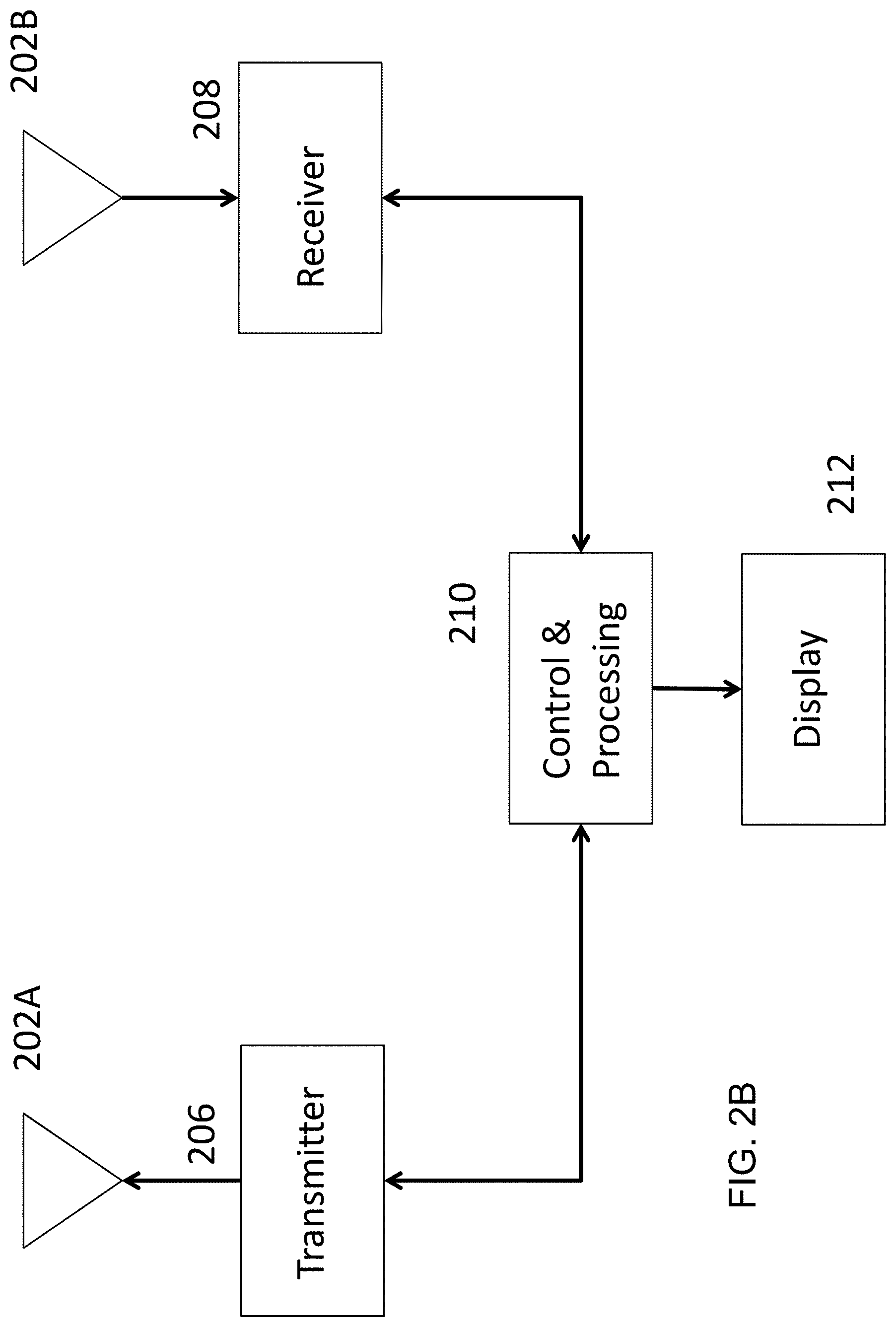
There are several ways to implement a radar system. One way, illustrated in FIG. 2A, uses a single antenna 202 for transmitting and receiving. The antenna 202 is connected to a duplexer 204 that routes the appropriate signal from the antenna 202 to a receiver 208 or routes the signal from a transmitter 206 to the antenna 202. A control processor 210 controls the operation of the transmitter 206 and the receiver 208 and estimates the range and velocity of objects in the environment. A second way to implement a radar system is shown in FIG. 2B. In this system, there are separate antennas for transmitting (202A) and receiving (202B). A control processor 210 performs the same basic functions as in FIG. 2A. In each case, there may be a display 212 to visualize the location of objects in the environment.
A radar system with multiple antennas, transmitters and receivers is shown in FIG. 3. Using multiple antennas 302, 304 allows an exemplary radar system 300 to determine the angle (azimuth or elevation or both) of targets in the environment. Depending on the geometry of the antenna system different angles (e.g., azimuth or elevation) can be determined.
The radar system 300 may be connected to a network via an Ethernet connection or other types of network connections 314, such as, for example, CAN-FD and FlexRay. The radar system 300 may also have memory (310, 312) to store software used for processing the signals in order to determine range, velocity and location of objects. Memory 310, 312 may also be used to store information about targets in the environment. There may also be processing capability contained in the ASIC 208 apart from the transmitters 203 and receivers 204.
The description herein includes an exemplary radar system in which there are NT transmitters and NR receivers for NT.times.NR virtual radars, one for each transmitter-receiver pair. For example, a radar system with eight transmitters and eight receivers will have 64 pairs or 64 virtual radars (with 64 virtual receivers). When three transmitters (Tx1, Tx2, Tx3) generate signals that are being received by three receivers (Rx1, Rx2, Rx3), each of the receivers is receiving the transmission from each of the transmitters reflected by objects in the environment. Each receiver can attempt to determine the range and Doppler of objects by correlating with delayed replicas of the signal from each of the transmitters. The physical receivers may then be "divided" into three separate virtual receivers, each virtual receiver correlating with delay replicas of one of the transmitted signals.
There are several different types of signals that transmitters in radar systems employ. A radar system may transmit a pulsed signal or a continuous signal. In a pulsed radar system, the signal is transmitted for a short time and then no signal is transmitted. This is repeated over and over. When the signal is not being transmitted, the receiver listens for echoes or reflections from objects in the environment. Often a single antenna is used for both the transmitter and receiver and the radar transmits on the antenna and then listens to the received signal on the same antenna. This process is then repeated. In a continuous wave radar system, the signal is continuously transmitted. There may be an antenna for transmitting and a separate antenna for receiving.
Another classification of radar systems is the modulation of signal being transmitted. A first type of continuous wave radar signal is known as a frequency modulated continuous wave (FMCW) radar signal. In an FMCW radar system, the transmitted signal is a sinusoidal signal with a varying frequency. By measuring a time difference between when a certain frequency was transmitted and when the received signal contained that frequency, the range to an object can be determined. By measuring several different time differences between a transmitted signal and a received signal, velocity information can be obtained.
A second type of continuous wave signal used in radar systems is known as a phase modulated continuous wave (PMCW) radar signal. In a PMCW radar system, the transmitted signal from a single transmitter is a sinusoidal signal in which the phase of the sinusoidal signal varies. Typically, the phase during a given time period (called a chip period or chip duration) is one of a finite number of possible phases. A spreading code consisting of a sequence of chips, (e.g., +1, +1, -1, +1, -1 . . . ) is mapped (e.g., +1.fwdarw.0, -1.fwdarw..pi.) into a sequence of phases (e.g., 0, 0, .pi., 0, .pi. . . . ) that is used to modulate a carrier to generate the radio frequency (RF) signal. The spreading code could be a periodic sequence or could be a pseudo-random sequence with a very large period so it appears to be a nearly random sequence. The spreading code could be a binary code (e.g., +1 or -1). The resulting signal has a bandwidth that is proportional to the rate at which the phases change, called the chip rate R.sub.c, which is the inverse of the chip duration T.sub.c=1/R.sub.c. By comparing the return signal to the transmitted signal, the receiver can determine the range and the velocity of reflected objects.
In some radar systems, the signal (e.g. a PMCW signal) is transmitted over a short time period (e.g. 1 microsecond) and then turned off for a similar time period. The receiver is only turned on during the time period where the transmitter is turned off. In this approach, reflections of the transmitted signal from very close targets will not be completely available because the receiver is not active during a large fraction of the time when the reflected signals are being received. This is called pulse mode.
The radar sensing system of the present invention may utilize aspects of the radar systems described in U.S. Pat. Nos. 9,846,228; 9,806,914; 9,791,564; 9,791,551; 9,772,397; 9,753,121; 9,599,702; 9,575,160 and/or 9,689,967, and/or U.S. Publication Nos. US-2017-0309997; US-2017-0307728 and/or US-2017-0310758, and/or U.S. patent application Ser. No. 15/496,038, filed Apr. 25, 2017, Ser. No. 15/689,273, filed Aug. 29, 2017, and/or Ser. No. 15/705,627, filed Sep. 15, 2017, and/or U.S. provisional applications, Ser. No. 62/486,732, filed Apr. 18, 2017, Ser. No. 62/528,789, filed Jul. 5, 2017, Ser. No. 62/573,880, filed Oct. 18, 2017, Ser. No. 62/598,563, filed Dec. 14, 2017, and/or Ser. No. 62/623,092, filed Jan. 29, 2018, which are all hereby incorporated by reference herein in their entireties.
FIG. 4 illustrates an exemplary transmitter 400 and receiver 450 of a radar system. The transmitter 400 includes a digital processor 410 that generates a baseband transmitted signal. The baseband signal is converted to an analog signal by a digital-to-analog converter (DAC) 420 and then mixed up to a carrier frequency and amplified by a radio frequency (RF) front end 430 before being radiated by an antenna 440. Each receiver 450 of the radar system generally will have a receive antenna 460, an analog RF front end 470 followed by an analog-to-digital converter (ADC) 480 that outputs complex valued digitized samples (i.e., values comprising a mathematical real component and a mathematical imaginary component) and a digital baseband processing section 490. The digital signal generator 410 (of the transmitter 400) and the digital baseband processing section 490 (of the receiver 450) need to know the sequence of spreading code chips used in generating the spreading code (e.g., for successful correlation of the received radio signals). This shared knowledge of the sequence of spreading code chips is illustrated with the dashed line connecting (410) and (490).
FIG. 5 illustrates a block diagram of the digital processing sections of the transmitter (410) and receiver (490) that includes an exemplary programmable code generation unit 510 that is communicatively coupled to each. Note that while FIG. 5 illustrates a single digital processing section 410 for the transmitter 400, there may be a plurality of digital processing sections 410 from a plurality of transmitters 400. Similarly, there can be a plurality of digital baseband processing sections 490 from a plurality of receivers 450. However, there is only one programmable code generation unit 510 used to generate all the spreading codes for the different transmitters 400 and used by the different receivers 450.
The digital baseband processing section 490 of a receiver 450 in a radar system will processes samples from the ADC 480. This processing involves calculating correlations with different delays of the baseband signal for each of the possible transmitted baseband signals. There are a variety of ways that the correlation process can be accomplished, including the use of a matched filter and Fourier transform processing. The processing for calculating correlations can be done for a set of distances. Each delay of the baseband signal corresponds to a range for a target. A range bin is the range corresponding to a certain delay of the baseband signal used in a correlation. The correlation with a particular delay is an indication of whether or not a target is present at the particular range. For example, a spreading code might have a chip rate of R.sub.c=500 Mchips/second which would correspond to a chip duration of T.sub.c=2 nanoseconds (ns). The receiver 450 might perform correlation delays at intervals of 2 ns, starting at a delay of 2 ns up to a maximum delay of 256 ns. That is, 128 different correlations would be performed. A target at a distance of 30 meters would produce a delay of 200 ns. A correlation with a baseband spreading code at a delay of 100 chips (200 ns) would produce a large magnitude output because the reflected signal off the target at 30 meters would produce a large correlation with the baseband spreading signal also delayed by 200 ns. While a target at a distance of 30.3 meters would produce a large correlation with a baseband signal delayed by 101 chips (202 ns). Therefore, targets at a distance between close to 30 meters (e.g. within .+-.0.15 meters would produce larger outputs when correlated with a baseband signal delay by 100 chips than a baseband signal delayed by either 99 chips or 101 chips. The range bin then corresponding to 30 meters would be of a width of 0.3 meters. A correlation unit might be set up to produce a certain set of correlations (e.g. 128 correlations for range bins starting at 0.3 meters to a distance of 38.4 meters). In other words, a correlation unit might be capable of producing a certain number of correlations or determine the presence of targets in a certain set of range bins. A correlation unit could be set up to consider different sets of range bins with which to perform correlations over.
Spreading codes with good autocorrelation functions are important so that the receiver can distinguish targets from different locations. Sometimes the spreading codes are called sequences and sometimes they are called codes. One type of spreading code is known as a maximal-length sequence or an m-sequence for short. This is also called a linear feedback shift register (LFSR) sequence. This might also be known as a pseudo-noise (PN) sequence. Therefore, such a generator may be known as a pseudo-random sequence generator (PRBS). FIG. 6 illustrates an exemplary shift register 600 used to generate an m-sequence. FIG. 6 illustrates that there are a number of memory elements 601-605 that form the shift register 600. The exemplary shift register 600 may have any number of elements and adders and is not limited to the number of elements and adders, or their arrangement, illustrated in FIG. 6. Each memory element 601-605 stores a binary value 0 or 1. The shift register has a clock signal (not shown) in which at every clock cycle the contents of the memory elements 601-605 are shifted to the right and a linear combination (606-608) of the elements are used to generate a bit stored in the left most element (601). The adders (606-608) are binary modulo two adders. That is, 0+0=0, 0+1=1, and 1+1=0.
The sequence of output of the far-right element (605) is the m-sequence. This sequence has a number of properties. The generated sequence, x.sub.n, is a periodic sequence. This is because there are a finite number of possible contents (states) of the shift register 600. Every time the shift register 600 is in a certain state, the sequence of states subsequently is identical. If the shift register 600 is ever in an all-zero state (where every element contains the binary value 0) then the shift register 600 will remain in the all zero state and the output will be a binary value 0 always. If there are m elements in the shift register 600, then it is possible for the state to be one of 2.sup.m possible values. However, as indicated above, the all zero state produces a trivial sequence of all zeros. There are 2.sup.m-1 possible nonzero states. If the shift register 600 goes through all these states before repeating, then the sequence will repeat with period L.sub.c=2.sup.m-1. This sequence is known as a maximal length sequence because it is the maximum length sequence that can be produced by a shift register 600 of length m. The method to generate the sequence, illustrated in FIG. 6, is known as the Fibonacci implementation. Another implementation of the same spreading code is illustrated in FIG. 7, and is known as the Galois implementation.
In FIG. 7, modulo two adders (706-708) are positioned between certain memory elements (701-705). The sequences generated by the two implementations are the same, provided that the connections for the Galois implementation are the reverse of the connections shown for the Fibonacci implementation. Only certain feedback connections used in the shift register will generate maximal length sequences. Other feedback connections will generate sequences of length that are smaller than the maximum length that is generated by an m-sequence generator. The appropriate feedback connections are widely tabulated for shift registers of moderate size (e.g. m<30).
Often, the sequence of 1s and 0s is converted to a binary sequence of +1's and -1s. There are two possible mappings, either 0.fwdarw.+1, 1.fwdarw.-1 or 0.fwdarw.-1, 1.fwdarw.+1. If the former is used, then adding modulo 2 in the 0, 1 domain is the same as multiplication in the +1, -1 domain. If the sequence generated consisting of 1s and 0s is converted to +1 s and -1s and called u.sub.n, n=0, 1, 2, . . . , then the periodic autocorrelation of the sequence u.sub.n has a two-level property. The periodic autocorrelation of the sequence u.sub.n is:
.theta..function..times..times. ##EQU00001## where either the sequence is an infinite length periodic sequence with period L.sub.c or the index on u.sub.n+l is determined modulo L.sub.c. The autocorrelation function is the correlation between the sequence u.sub.n and the same sequence with offset l, namely u.sub.n+l. Note that in the case where the sequence contains complex numbers, u.sub.n* is the complex conjugate of u.sub.n. The periodic autocorrelation .theta..sub.u(l) of an m-sequence (converted to a +1, -1 sequence) is L.sub.c (mod L.sub.c), if =0 and .theta..sub.u(l)=-1, if l(mod L.sub.c)=1, 2, . . . , N-1. This is illustrated in FIG. 8 for an m-sequence of length/period L.sub.c=127, including a zoomed-in portion which shows that when l.noteq.0 mod(L.sub.c), the autocorrelation is -1.
Another autocorrelation function is the aperiodic autocorrelation function. This is defined as
.function..times..times..times..times..ltoreq..ltoreq. ##EQU00002## ##EQU00002.2## .function..times..times..times..times..ltoreq..ltoreq. ##EQU00002.3##
This autocorrelation is important when the signal transmitted consists of a single period of a spreading code, as opposed to multiple periods of a spreading code. One important spreading code with good aperiodic autocorrelation is the Barker code. There are a limited number of possible Barker codes of lengths up to L.sub.c=13. These are shown in the Table below. The aperiodic autocorrelation of Barker codes is no larger in absolute value than 1. The aperiodic autocorrelation is illustrated in FIG. 9 for the Barker code of length 11.
TABLE-US-00001 L.sub.c Code 2 +1, -1 3 +1, +1, -1 4 +1, +1, -1, +1 5 +1, +1, +1, -1, +1 7 +1, +1, +1, -1, -1, +1, -1 11 +1, +1, +1, -1, -1, -1, +1, -1, -1, +1, -1 13 +1, +1, +1, +1, +1, -1, -1, +1, +1, -1, +1, -1, +1
Another class of codes is the Frank-Zadoff-Chu codes. Unlike Barker codes or m-sequences, which are binary codes, the Frank-Zadoff-Chu codes are sequences of complex numbers, where each complex number is on the unit circle. That is, a plot of each sequence element on the complex plane (real part is the horizontal axis, imaginary part is the vertical axis) lies on the unit circle. The codes can be defined when L.sub.c is even, as
.times..pi..times..times..times..times..times..times..times..times..pi..t- imes..function..times..times. ##EQU00003## for when L.sub.c is odd. The value of the periodic autocorrelation function .theta..sub.u(l) is L.sub.c for l mod (L.sub.c)=0, and is 0 for l mod (L.sub.c).noteq.0. This is the ideal autocorrelation. Note that, in general for complex sequences, the autocorrelation function is a complex number which contains a real part and an imaginary part. Two real correlations are needed to compute the real part of the autocorrelation and two real correlations are needed to compute the imaginary part of the correlation. Generally, the received signal after down-conversion and sampling is a complex number. For real transmitted sequences, two correlations are needed: a correlation of the real transmitted sequence with the real part of the received sequence and a correlation of the real transmitted sequence with the imaginary part of the received sequence. For FZC sequences, the periodic autocorrelation function is (ideally) purely real. That is, the imaginary part is zero. The real part of the periodic autocorrelation is illustrated in FIG. 10 for the case of L.sub.c=32. For L.sub.c=6, the FZC sequence corresponds to points on the unit circle with angles with respect to the positive horizontal axis of [0, -30, -120, 90, -120, -30]. While these codes have the ideal autocorrelation function, they also generate complex (as opposed to purely real) spreading codes. Furthermore, the real and imaginary parts of the code are not just binary (e.g. +1, -1) values, but can also be arbitrary numbers. For example, the second component of the above sequence is the complex number
##EQU00004## where j= {square root over ((-1))}.
There are various other codes, including Golay codes, almost perfect autocorrelation sequences (APAS), and Hadamard codes. Codes with good autocorrelation functions are desired in a radar system. Complex codes require more storage than binary codes. Long codes are generally desirable because the autocorrelation function is generally better, the longer the code. Generating codes at a high chip rate is also desirable. Furthermore, codes that are unpredictable are also desirable.
Codes used for different transmitters that have low cross-correlation are desirable. The periodic cross-correlation function between a code sequence u.sub.l, l=0, 1, . . . , L.sub.c-1 and a code sequence v.sub.l, l=0, 1, . . . , L.sub.c-1 is defined as:
.theta..function..times..times. ##EQU00005## where again either the code sequence repeats or the index for the sequences are determined modulo L.sub.c. One class of codes with interesting cross-correlation properties is known as Gold codes. The Gold codes can be formed from two m-sequences of the same length. FIG. 11 illustrates an exemplary way to generate a Gold code. The method illustrated in FIG. 11 involves modulo 2 adding (1130) the output of two m-sequence generators (1110) and (1120). Depending on the seed values, different Gold codes are generated. If either of the two (but not both) of the generators (1110, 1120) is started with all zeros in the shift register, then the output is just the m-sequence of the other shift register and this is considered one of the Gold codes. By changing the nonzero seed of one m-sequence generator with respect to the seed of the other m-sequence generator, different codes are generated. For the example illustrated in FIG. 11, where the shift register has 5 memory elements and the m-sequences generated are of length 31, there are 33 possible Gold codes. The autocorrelation properties of Gold codes are not as good as m-sequences, but there are more such sequences. For example, there are only 3 m-sequences of length 31 (not counting reverses of an m-sequence), but there are 33 possible Gold codes. There are alternative ways of implementing Gold code generators, known in the art, including using a single shift register of a length that is twice the length of the individual shift registers illustrated in FIG. 11. That is, a single shift register of length 10, with appropriate feedback connections, can generate different Gold codes depending on the initial contents.
Another set of codes are the Hadamard codes, which can be defined recursively when the length is a power of 2. Namely
##EQU00006## ##EQU00006.2## ##EQU00006.3##
The rows in a Hadamard matrix are orthogonal. That is, the periodic cross correlation between two sequences u and v is 0, at offset 0; .theta..sub.u,v(0)=0. This is useful when different rows of a Hadamard matrix are used as the spreading codes. However, the autocorrelation of the codes is not good. A combination of codes is possible that have good autocorrelation function properties, and are orthogonal as well, when the sequences are synchronized at different transmitters.
In one embodiment, an exemplary spreading code is generated from several constituent codes. This is illustrated in FIG. 12. A first constituent code is a spreading code of length L.sub.c chips (1240). This could be an m-sequence (PRBS) generated by a shift register. This code can be repeated M times (1230), where M.gtoreq.1, and then the code is combined with a Hadamard code of size K (1220) across different transmitters. This combination is then varied for N.sub.FFT times (1210). The total length of the spreading code is then L.sub.cM K N.sub.FFT. In this case, the Hadamard code is combined with, for example, an m-sequence generated in a feedback shift register repeated M times. There is additional possible variation on the spreading code, in the case when a Golay code is used. Because the Golay code requires two constituent codes, for which the sum of the autocorrelation functions has desirable properties, there is an additional requirement of transmitting two codes of length L.sub.c, so that the overall spreading code length is now 2 L.sub.c M K N.sub.FFT.
One way to combine different sequences is via a Kronecker product operation. The Kronecker product of a sequence x.sub.1, x.sub.2, x.sub.3 that is of length 3, with a sequence y.sub.1, y.sub.2, that is of length 2, is the sequence x.sub.1y.sub.1, x.sub.2y.sub.1, x.sub.3y.sub.1, x.sub.1y.sub.2, x.sub.2y.sub.2, x.sub.3y.sub.2, that is of length 6.
While it is possible to use a conventional general-purpose processor to generate any possible code, the processor would need to operate with a clock cycle several times as fast as the chip rate. A chip rate of 1 Gchips/second would require a processor that is difficult or costly to implement. In one embodiment illustrated in FIG. 13, an exemplary programmable code generation unit 1300 includes a control processor 1301, a memory 1302, programmable shift registers 1303, a combinatorial logic 1304, a DC balancing subsystem 1305, and a Hadamard processing subsystem 1306. The structure of the programmable code generator 1300 contains a processor 1301 that can access the memory 1302, control the shift registers 1303, the combinatorial logic 1304, the DC balancing subsystem 1305, and the Hadamard processing subsystem 1306.
The programmable code generator 1300 contains preferably 48 shift registers of 31 memory elements each, that can be programmed to generate any desired feedback connection, as well as loaded with any seed sequence. The shift registers 1303 can be programmed to generate an m-sequence of length 2.sup.31-1. The feedback shift registers 1303 can also be shortened in length via feeding back from any set of desired elements in the register which might not include the last element. In this implementation, the last element and potentially other elements, become pure delay elements. The feedback shift register generators can be loaded with any contents (sometimes called the seed) and generators can be configured via software to have any set of feedback connections desired. The structure of the programmable code generator 1300 also has memory 1302 that can store chips used in an arbitrary sequence up to the size of the memory 1302. For example, the memory 1302 could store Hadamard sequences that are read by the processor 1301 and then combined with shift register sequences in the Hadamard processing block 1306. The memory 1302 can store actual chip sequences for different transmitters. One mode of operation, known as range domain MIMO, uses the full memory to provide a first chip sequence for one transmitter. The sequences for the other transmitters are then delayed versions of the first chip sequence. In one embodiment, the memory 1302 has the storage capacity to allow for 12 sequences of length 192K chips.
The memory 1302 can store the seeds and taps to control the feedback shift registers 1303. The processor 1301 can pick a random seed for the shift registers 1303 to choose different sequences instead of deterministically traversing the memory 1302 in a fixed sequence.
The combinatorial logic 1304 can be used for a variety of purposes. In one embodiment, the combinatorial logic 1304 performs exclusive OR (XOR) operations on different streams and can also be used to define which shift register stream goes to which transmitter. Alternatively, one code may be forwarded to all transmitters.
In one embodiment, the DC balancer 1305 first tracks the DC balance. The DC balance is the sum of the quantity of chips that take a value=1 in the past/chips, minus the sum of the quantity of chips that take a value=0 over the same interval. The DC balancer 1305 can be configured to control a maximum absolute value of the DC balance a chip stream may have, called the DC threshold. The DC threshold is configurable but preferably 20. Once the DC balance reaches the threshold the DC balancer will flip the next chip if that chip would cause the DC balance to exceed the DC threshold. Otherwise the DC balancer need not flip the next bit and the DC balance will improve. If the chip sequence is a finite length sequence then the DC balancer can force the DC balance to zero at the end of the sequence by forcing the appropriate last number of bits (e.g. 20) so that the DC balance at the end is zero. Alternatively, the DC balancer can slowly decrease the maximum DC balance threshold when the number of chips left in the finite sequence is smaller than some value. For example, for a sequence of length 512 with a maximum DC balance of 20 when there are 60 chips left in the sequence the DC balancer can reduce the maximum DC balance by 1 every three chips. So that by the time there are only 3 chips left the DC balance is at most 1. At that point, it can reduce the DC balance to zero by forcing the last chip to a value that causes the DC balance to 0 over the whole sequence.
The DC balancer 1305 may also flip an entire sequence of bits, or may take the previous sequence of bits over a range of bits, flip all the bits in the sequence and then used the flipped bits as the spreading code. The DC balancer can also take the flipped bits and do a permutation of the sequence of flipped bits and transmit that sequence. The DC balancer may insert either zeros or ones (0s, 1s) into any of the chip sequences as well.
The DC balancer 1305 may also balance the code across different transmitters over a configured interval. The DC balancer with multiple transmitters checks the DC balance across the different transmitters. If the absolute DC balance across transmitters exceeds a threshold then the DC balancer can change a chip in one of the transmitters. For example, if the DC balance across all transmitters for an individual chip in each of the transmitters exceeds the maximum value then the individual sequence with the worst DC balance in that individual sequence for which changing that chip can improve the DC balance across transmitters and improve the DC balance for the individual transmitter will have that chip flipped in sign. For example, suppose that there are eight transmitters and the individual DC balance for these transmitters is 2, -6, 8, -18, 12, -2, 3, 1 and for a particular chip the DC balance across transmitters is above a threshold, such as the eight chips are 0, 0, 1, 0, 0, 1, 0, 1. Then the DC balancer would need to change one of these chips from a 0 to a 1 in order to have a better balance. One of the transmitters that has a chip of 0 would need to change to 1 in order to improve the DC balance across chips. Transmitters 1, 3, 5, 7, and 8 have more ones than zeros while transmitters 2, 4, and 6 have more zeros than ones. The transmitter that would be changed would flip the bit would be transmitter 5 which would change the balance across transmitters to 2, -6, 8, -18, 10, -2, 3, 1 because what was a one before is removed and an addition zero is added to the balance for transmitter 5. While this will work to keep the DC balance across transmitters when the threshold for balancing an individual transmitter is reduced near the end of a sequence, the balance across transmitters can be eliminated because simultaneous balancing might require look ahead for the chip sequence.
* * * * *
References
D00000
D00001
D00002
D00003
D00004
D00005
D00006
D00007
D00008
D00009
D00010
D00011
D00012

D00013

D00014

M00001

M00002

M00003

M00004

M00005

M00006

XML
uspto.report is an independent third-party trademark research tool that is not affiliated, endorsed, or sponsored by the United States Patent and Trademark Office (USPTO) or any other governmental organization. The information provided by uspto.report is based on publicly available data at the time of writing and is intended for informational purposes only.
While we strive to provide accurate and up-to-date information, we do not guarantee the accuracy, completeness, reliability, or suitability of the information displayed on this site. The use of this site is at your own risk. Any reliance you place on such information is therefore strictly at your own risk.
All official trademark data, including owner information, should be verified by visiting the official USPTO website at www.uspto.gov. This site is not intended to replace professional legal advice and should not be used as a substitute for consulting with a legal professional who is knowledgeable about trademark law.