Memory array with individually trimmable sense amplifiers
Karmakar , et al. February 23, 2
U.S. patent number 10,930,332 [Application Number 16/520,162] was granted by the patent office on 2021-02-23 for memory array with individually trimmable sense amplifiers. This patent grant is currently assigned to Spin Memory, Inc.. The grantee listed for this patent is SPIN MEMORY, INC.. Invention is credited to Neal Berger, Mourad El Baraji, Susmita Karmakar, Benjamin Louie.


| United States Patent | 10,930,332 |
| Karmakar , et al. | February 23, 2021 |
Memory array with individually trimmable sense amplifiers
Abstract
A device includes an array of memory cells, input/output lines coupled to the memory cells, and sense amplifiers coupled to the input/output lines. Each sense amplifier is associated with a respective input/output line. The device also includes trim circuits. Each trim circuit is associated with and coupled to a respective sense amplifier. Each sense amplifier receives a respective reference voltage that allows the sense amplifier to sense a bit value of an addressed memory cell. Each trim circuit is operable for compensating for variations in the reference voltage used by the respective sense amplifier.
| Inventors: | Karmakar; Susmita (Fremont, CA), Berger; Neal (Cupertino, CA), El Baraji; Mourad (Fremont, CA), Louie; Benjamin (Fremont, CA) | ||||||||||
|---|---|---|---|---|---|---|---|---|---|---|---|
| Applicant: |
|
||||||||||
| Assignee: | Spin Memory, Inc. (Fremont,
CA) |
||||||||||
| Family ID: | 67058431 | ||||||||||
| Appl. No.: | 16/520,162 | ||||||||||
| Filed: | July 23, 2019 |
Prior Publication Data
| Document Identifier | Publication Date | |
|---|---|---|
| US 20190348097 A1 | Nov 14, 2019 | |
Related U.S. Patent Documents
| Application Number | Filing Date | Patent Number | Issue Date | ||
|---|---|---|---|---|---|
| 15857296 | Jul 23, 2019 | 10360962 | |||
| Current U.S. Class: | 1/1 |
| Current CPC Class: | G11C 11/1693 (20130101); G11C 29/028 (20130101); G11C 29/026 (20130101); G11C 11/1655 (20130101); G11C 7/08 (20130101); G11C 11/1673 (20130101); G11C 7/062 (20130101); G11C 2207/002 (20130101) |
| Current International Class: | G11C 11/16 (20060101); G11C 7/08 (20060101); G11C 7/06 (20060101) |
| Field of Search: | ;365/158,171 |
References Cited [Referenced By]
U.S. Patent Documents
| 4597487 | July 1986 | Crosby et al. |
| 5541868 | July 1996 | Prinz |
| 5559952 | September 1996 | Fujimoto |
| 5629549 | May 1997 | Johnson |
| 5640343 | June 1997 | Gallagher et al. |
| 5654566 | August 1997 | Johnson |
| 5691936 | November 1997 | Sakakima et al. |
| 5694936 | November 1997 | Sakahima et al. |
| 5695846 | December 1997 | Lange et al. |
| 5695864 | December 1997 | Slonczewski |
| 5732016 | March 1998 | Chen et al. |
| 5751647 | May 1998 | O'Toole |
| 5856897 | January 1999 | Mauri |
| 5896252 | April 1999 | Kanai |
| 5966323 | October 1999 | Chen et al. |
| 6016269 | January 2000 | Peterson et al. |
| 6055179 | April 2000 | Koganei et al. |
| 6064948 | May 2000 | West |
| 6075941 | June 2000 | Itoh |
| 6097579 | August 2000 | Gill |
| 6112295 | August 2000 | Bhamidipati et al. |
| 6124711 | September 2000 | Tanaka et al. |
| 6134138 | October 2000 | Lu et al. |
| 6140838 | October 2000 | Johnson |
| 6154139 | November 2000 | Kanai et al. |
| 6154349 | November 2000 | Kanai et al. |
| 6172902 | January 2001 | Wegrowe et al. |
| 6233172 | May 2001 | Chen et al. |
| 6233690 | May 2001 | Choi et al. |
| 6243288 | June 2001 | Ishikawa et al. |
| 6252798 | June 2001 | Satoh et al. |
| 6256223 | July 2001 | Sun |
| 6292389 | September 2001 | Chen et al. |
| 6347049 | February 2002 | Childress et al. |
| 6376260 | April 2002 | Chen et al. |
| 6385082 | May 2002 | Abraham et al. |
| 6436526 | August 2002 | Odagawa et al. |
| 6442681 | August 2002 | Ryan et al. |
| 6447935 | September 2002 | Zhang et al. |
| 6458603 | October 2002 | Kersch et al. |
| 6493197 | December 2002 | Ito et al. |
| 6522137 | February 2003 | Sun et al. |
| 6532164 | March 2003 | Redon et al. |
| 6538918 | March 2003 | Swanson et al. |
| 6545903 | April 2003 | Savtchenko et al. |
| 6545906 | April 2003 | Savtchenko et al. |
| 6563681 | May 2003 | Sasaki et al. |
| 6566246 | May 2003 | deFelipe et al. |
| 6603677 | August 2003 | Redon et al. |
| 6608776 | August 2003 | Hidaka |
| 6635367 | October 2003 | Igarashi et al. |
| 6653153 | November 2003 | Doan et al. |
| 6654278 | November 2003 | Engel et al. |
| 6677165 | January 2004 | Lu et al. |
| 6710984 | March 2004 | Yuasa et al. |
| 6713195 | March 2004 | Wang et al. |
| 6714444 | March 2004 | Huai et al. |
| 6731537 | May 2004 | Kanamori |
| 6744086 | June 2004 | Daughton et al. |
| 6750491 | June 2004 | Sharma et al. |
| 6751074 | June 2004 | Inomata et al. |
| 6765824 | July 2004 | Kishi et al. |
| 6772036 | August 2004 | Eryurek et al. |
| 6773515 | August 2004 | Li et al. |
| 6777730 | August 2004 | Daughton et al. |
| 6785159 | August 2004 | Tuttle |
| 6807091 | October 2004 | Saito |
| 6812437 | November 2004 | Levy et al. |
| 6829161 | December 2004 | Huai et al. |
| 6835423 | December 2004 | Chen et al. |
| 6838740 | January 2005 | Huai et al. |
| 6839821 | January 2005 | Estakhri |
| 6842317 | January 2005 | Sugita et al. |
| 6842366 | January 2005 | Chan |
| 6847547 | January 2005 | Albert et al. |
| 6879512 | April 2005 | Luo |
| 6887719 | May 2005 | Lu et al. |
| 6888742 | May 2005 | Nguyen et al. |
| 6902807 | June 2005 | Argoitia et al. |
| 6906369 | June 2005 | Ross et al. |
| 6920063 | July 2005 | Huai et al. |
| 6933155 | August 2005 | Albert et al. |
| 6936479 | August 2005 | Sharma |
| 6938142 | August 2005 | Pawlowski |
| 6956257 | October 2005 | Zhu et al. |
| 6958507 | October 2005 | Atwood et al. |
| 6958927 | October 2005 | Nguyen et al. |
| 6967863 | November 2005 | Huai |
| 6980469 | December 2005 | Kent et al. |
| 6984529 | January 2006 | Stojakovic et al. |
| 6985385 | January 2006 | Nguyen et al. |
| 6992359 | January 2006 | Nguyen et al. |
| 6995962 | February 2006 | Saito et al. |
| 7002839 | February 2006 | Kawabata et al. |
| 7005958 | February 2006 | Wan |
| 7006371 | February 2006 | Matsuoka |
| 7006375 | February 2006 | Covington |
| 7009877 | March 2006 | Huai et al. |
| 7033126 | April 2006 | Van Den Berg |
| 7041598 | May 2006 | Sharma |
| 7045368 | May 2006 | Hong et al. |
| 7054119 | May 2006 | Sharma et al. |
| 7057922 | June 2006 | Fukumoto |
| 7095646 | August 2006 | Slaughter et al. |
| 7098494 | August 2006 | Pakala et al. |
| 7106624 | September 2006 | Huai et al. |
| 7110287 | September 2006 | Huai et al. |
| 7149106 | December 2006 | Mancoff et al. |
| 7161829 | January 2007 | Huai et al. |
| 7170778 | January 2007 | Kent et al. |
| 7187577 | March 2007 | Wang |
| 7190611 | March 2007 | Nguyen et al. |
| 7203129 | April 2007 | Lin et al. |
| 7203802 | April 2007 | Huras |
| 7227773 | June 2007 | Nguyen et al. |
| 7233039 | June 2007 | Huai et al. |
| 7242045 | July 2007 | Nguyen et al. |
| 7245462 | July 2007 | Huai et al. |
| 7262941 | August 2007 | Li et al. |
| 7273780 | September 2007 | Kim |
| 7283333 | October 2007 | Gill |
| 7307876 | December 2007 | Kent et al. |
| 7313015 | December 2007 | Bessho |
| 7324387 | January 2008 | Bergemont et al. |
| 7324389 | January 2008 | Cernea |
| 7335960 | February 2008 | Han et al. |
| 7351594 | April 2008 | Bae et al. |
| 7352021 | April 2008 | Bae et al. |
| 7369427 | May 2008 | Diao et al. |
| 7372722 | May 2008 | Jeong |
| 7376006 | May 2008 | Bednorz et al. |
| 7386765 | June 2008 | Ellis |
| 7404017 | July 2008 | Kuo |
| 7421535 | September 2008 | Jarvis et al. |
| 7436699 | October 2008 | Tanizaki |
| 7449345 | November 2008 | Horng et al. |
| 7453719 | November 2008 | Sakimura |
| 7476919 | January 2009 | Hong et al. |
| 7502249 | March 2009 | Ding |
| 7502253 | March 2009 | Rizzo |
| 7508042 | March 2009 | Guo |
| 7511985 | March 2009 | Horii |
| 7515458 | April 2009 | Hung et al. |
| 7515485 | April 2009 | Lee |
| 7532503 | May 2009 | Morise et al. |
| 7541117 | June 2009 | Ogawa |
| 7542326 | June 2009 | Yoshimura |
| 7573737 | August 2009 | Kent et al. |
| 7576956 | August 2009 | Huai |
| 7582166 | September 2009 | Lampe |
| 7598555 | October 2009 | Papworth-Parkin |
| 7602000 | October 2009 | Sun et al. |
| 7619431 | November 2009 | DeWilde et al. |
| 7633800 | December 2009 | Adusumilli et al. |
| 7642612 | January 2010 | Izumi et al. |
| 7663171 | February 2010 | Inokuchi et al. |
| 7696551 | April 2010 | Xiao |
| 7733699 | June 2010 | Roohparvar |
| 7739559 | June 2010 | Suzuki et al. |
| 7773439 | August 2010 | Do et al. |
| 7776665 | August 2010 | Izumi et al. |
| 7796439 | September 2010 | Arai |
| 7810017 | October 2010 | Radke |
| 7821818 | October 2010 | Dieny et al. |
| 7852662 | December 2010 | Yang |
| 7861141 | December 2010 | Chen |
| 7881095 | February 2011 | Lu |
| 7911832 | March 2011 | Kent et al. |
| 7916515 | March 2011 | Li |
| 7936595 | May 2011 | Han et al. |
| 7936598 | May 2011 | Zheng et al. |
| 7983077 | July 2011 | Park |
| 7986544 | July 2011 | Kent et al. |
| 8008095 | August 2011 | Assefa et al. |
| 8028119 | September 2011 | Miura |
| 8041879 | October 2011 | Erez |
| 8055957 | November 2011 | Kondo |
| 8058925 | November 2011 | Rasmussen |
| 8059460 | November 2011 | Jeong et al. |
| 8072821 | December 2011 | Arai |
| 8077496 | December 2011 | Choi |
| 8080365 | December 2011 | Nozaki |
| 8088556 | January 2012 | Nozaki |
| 8094480 | January 2012 | Tonomura |
| 8102701 | January 2012 | Prejbeanu et al. |
| 8105948 | January 2012 | Zhong et al. |
| 8116117 | February 2012 | Cho |
| 8120949 | February 2012 | Ranjan et al. |
| 8143683 | March 2012 | Wang et al. |
| 8144509 | March 2012 | Jung |
| 8148970 | April 2012 | Fuse |
| 8159867 | April 2012 | Cho et al. |
| 8201024 | June 2012 | Burger |
| 8223534 | July 2012 | Chung |
| 8243542 | August 2012 | Bae |
| 8255842 | August 2012 | Ipek |
| 8278996 | October 2012 | Miki |
| 8279666 | October 2012 | Dieny et al. |
| 8295073 | October 2012 | Norman |
| 8295082 | October 2012 | Chua-Eoan |
| 8334213 | December 2012 | Mao |
| 8345474 | January 2013 | Oh |
| 8349536 | January 2013 | Nozaki |
| 8362580 | January 2013 | Chen et al. |
| 8363465 | January 2013 | Kent et al. |
| 8374050 | February 2013 | Zhou et al. |
| 8386836 | February 2013 | Burger |
| 8415650 | April 2013 | Greene |
| 8416620 | April 2013 | Zheng et al. |
| 8422286 | April 2013 | Ranjan et al. |
| 8422330 | April 2013 | Hatano et al. |
| 8432727 | April 2013 | Ryu |
| 8441844 | May 2013 | El Baraji |
| 8456883 | June 2013 | Liu |
| 8456926 | June 2013 | Ong et al. |
| 8477530 | July 2013 | Ranjan et al. |
| 8492881 | July 2013 | Kuroiwa et al. |
| 8495432 | July 2013 | Dickens |
| 8535952 | September 2013 | Ranjan et al. |
| 8539303 | September 2013 | Lu |
| 8542524 | September 2013 | Keshtbod et al. |
| 8549303 | October 2013 | Fifield et al. |
| 8558334 | October 2013 | Ueki et al. |
| 8559215 | October 2013 | Zhou et al. |
| 8574928 | November 2013 | Satoh et al. |
| 8582353 | November 2013 | Lee |
| 8590139 | November 2013 | Op DeBeeck et al. |
| 8592927 | November 2013 | Jan |
| 8593868 | November 2013 | Park |
| 8609439 | December 2013 | Prejbeanu et al. |
| 8617408 | December 2013 | Balamane |
| 8625339 | January 2014 | Ong |
| 8634232 | January 2014 | Oh |
| 8667331 | March 2014 | Hori |
| 8687415 | April 2014 | Parkin et al. |
| 8705279 | April 2014 | Kim |
| 8716817 | May 2014 | Saida |
| 8716818 | May 2014 | Yoshikawa et al. |
| 8722543 | May 2014 | Belen |
| 8737137 | May 2014 | Choy et al. |
| 8755222 | June 2014 | Kent et al. |
| 8779410 | July 2014 | Sato et al. |
| 8780617 | July 2014 | Kang |
| 8792269 | July 2014 | Abedifard |
| 8802451 | August 2014 | Malmhall |
| 8810974 | August 2014 | Noel et al. |
| 8817525 | August 2014 | Ishihara |
| 8832530 | September 2014 | Pangal et al. |
| 8852760 | October 2014 | Wang et al. |
| 8853807 | October 2014 | Son et al. |
| 8860156 | October 2014 | Beach et al. |
| 8862808 | October 2014 | Tsukamoto et al. |
| 8867258 | October 2014 | Rao |
| 8883520 | November 2014 | Satoh et al. |
| 8902628 | December 2014 | Ha |
| 8966345 | February 2015 | Wilkerson |
| 8987849 | March 2015 | Jan |
| 9019754 | April 2015 | Bedeschi |
| 9025378 | May 2015 | Tokiwa |
| 9026888 | May 2015 | Kwok |
| 9030899 | May 2015 | Lee |
| 9036407 | May 2015 | Wang et al. |
| 9037812 | May 2015 | Chew |
| 9043674 | May 2015 | Wu |
| 9070441 | June 2015 | Otsuka et al. |
| 9070855 | June 2015 | Gan et al. |
| 9076530 | July 2015 | Gomez et al. |
| 9082888 | July 2015 | Kent et al. |
| 9104581 | August 2015 | Fee et al. |
| 9104595 | August 2015 | Sah |
| 9130155 | September 2015 | Chepulskyy et al. |
| 9136463 | September 2015 | Li |
| 9140747 | September 2015 | Kim |
| 9165787 | October 2015 | Kang |
| 9166155 | October 2015 | Deshpande |
| 9178958 | November 2015 | Lindamood |
| 9189326 | November 2015 | Kalamatianos |
| 9190471 | November 2015 | Yi et al. |
| 9196332 | November 2015 | Zhang et al. |
| 9229806 | January 2016 | Mekhanik et al. |
| 9229853 | January 2016 | Khan |
| 9231191 | January 2016 | Huang et al. |
| 9245608 | January 2016 | Chen et al. |
| 9250990 | February 2016 | Motwani |
| 9250997 | February 2016 | Kim et al. |
| 9251896 | February 2016 | Ikeda |
| 9257483 | February 2016 | Ishigaki |
| 9263667 | February 2016 | Pinarbasi |
| 9286186 | March 2016 | Weiss |
| 9298552 | March 2016 | Leem |
| 9299412 | March 2016 | Naeimi |
| 9317429 | April 2016 | Ramanujan |
| 9324457 | April 2016 | Takizama |
| 9337412 | May 2016 | Pinarbasi et al. |
| 9341939 | May 2016 | Yu et al. |
| 9342403 | May 2016 | Keppel et al. |
| 9349482 | May 2016 | Kim et al. |
| 9351899 | May 2016 | Bose et al. |
| 9362486 | June 2016 | Kim et al. |
| 9378817 | June 2016 | Kawai |
| 9379314 | June 2016 | Park et al. |
| 9389954 | July 2016 | Pelley et al. |
| 9396065 | July 2016 | Webb et al. |
| 9396991 | July 2016 | Arvin et al. |
| 9401336 | July 2016 | Arvin et al. |
| 9406876 | August 2016 | Pinarbasi |
| 9418721 | August 2016 | Bose |
| 9431084 | August 2016 | Bose et al. |
| 9449720 | September 2016 | Lung |
| 9450180 | September 2016 | Annuziata |
| 9466789 | October 2016 | Wang et al. |
| 9472282 | October 2016 | Lee |
| 9472748 | October 2016 | Kuo et al. |
| 9484527 | November 2016 | Han et al. |
| 9488416 | November 2016 | Fujita et al. |
| 9490054 | November 2016 | Jan |
| 9508456 | November 2016 | Shim |
| 9520128 | December 2016 | Bauer et al. |
| 9520192 | December 2016 | Naeimi et al. |
| 9548116 | January 2017 | Roy |
| 9548445 | January 2017 | Lee et al. |
| 9553102 | January 2017 | Wang |
| 9583167 | February 2017 | Chung |
| 9594683 | March 2017 | Dittrich |
| 9600183 | March 2017 | Tomishima et al. |
| 9608038 | March 2017 | Wang et al. |
| 9634237 | April 2017 | Lee et al. |
| 9640267 | May 2017 | Tani |
| 9646701 | May 2017 | Lee |
| 9652321 | May 2017 | Motwani |
| 9662925 | May 2017 | Raksha et al. |
| 9697140 | July 2017 | Kwok |
| 9720616 | August 2017 | Yu |
| 9728712 | August 2017 | Kardasz et al. |
| 9741926 | August 2017 | Pinarbasi et al. |
| 9772555 | September 2017 | Park et al. |
| 9773974 | September 2017 | Pinarbasi et al. |
| 9780300 | October 2017 | Zhou et al. |
| 9793319 | October 2017 | Gan et al. |
| 9853006 | December 2017 | Arvin et al. |
| 9853206 | December 2017 | Pinarbasi et al. |
| 9853292 | December 2017 | Loveridge et al. |
| 9858976 | January 2018 | Ikegami |
| 9859333 | January 2018 | Kim et al. |
| 9865806 | January 2018 | Choi et al. |
| 9935258 | April 2018 | Chen et al. |
| 10008662 | June 2018 | You |
| 10026609 | July 2018 | Sreenivasan et al. |
| 10038137 | July 2018 | Chuang |
| 10042588 | August 2018 | Kang |
| 10043851 | August 2018 | Shen |
| 10043967 | August 2018 | Chen |
| 10062837 | August 2018 | Kim et al. |
| 10115446 | October 2018 | Louie et al. |
| 10134988 | November 2018 | Fennimore et al. |
| 10163479 | December 2018 | Berger et al. |
| 10186614 | January 2019 | Asami |
| 2002/0090533 | July 2002 | Zhang et al. |
| 2002/0105823 | August 2002 | Redon et al. |
| 2003/0085186 | May 2003 | Fujioka |
| 2003/0117840 | June 2003 | Sharma et al. |
| 2003/0151944 | August 2003 | Saito |
| 2003/0197984 | October 2003 | Inomata et al. |
| 2003/0218903 | November 2003 | Luo |
| 2004/0012994 | January 2004 | Slaughter et al. |
| 2004/0026369 | February 2004 | Ying |
| 2004/0061154 | April 2004 | Huai et al. |
| 2004/0094785 | May 2004 | Zhu et al. |
| 2004/0130936 | July 2004 | Nguyen et al. |
| 2004/0173315 | September 2004 | Leung |
| 2004/0257717 | December 2004 | Sharma et al. |
| 2005/0041342 | February 2005 | Huai et al. |
| 2005/0051820 | March 2005 | Stojakovic et al. |
| 2005/0063222 | March 2005 | Huai et al. |
| 2005/0104101 | May 2005 | Sun et al. |
| 2005/0128842 | June 2005 | Wei |
| 2005/0136600 | June 2005 | Huai |
| 2005/0158881 | July 2005 | Sharma |
| 2005/0180202 | August 2005 | Huai et al. |
| 2005/0184839 | August 2005 | Nguyen et al. |
| 2005/0201023 | September 2005 | Huai et al. |
| 2005/0237787 | October 2005 | Huai et al. |
| 2005/0280058 | December 2005 | Pakala et al. |
| 2006/0018057 | January 2006 | Huai |
| 2006/0049472 | March 2006 | Diao et al. |
| 2006/0077734 | April 2006 | Fong |
| 2006/0087880 | April 2006 | Mancoff et al. |
| 2006/0092696 | May 2006 | Bessho |
| 2006/0132990 | June 2006 | Morise et al. |
| 2006/0227465 | October 2006 | Inokuchi et al. |
| 2007/0019337 | January 2007 | Apalkov et al. |
| 2007/0096229 | May 2007 | Yoshikawa |
| 2007/0242501 | October 2007 | Hung et al. |
| 2008/0049488 | February 2008 | Rizzo |
| 2008/0079530 | April 2008 | Weidman et al. |
| 2008/0112094 | May 2008 | Kent et al. |
| 2008/0151614 | June 2008 | Guo |
| 2008/0259508 | October 2008 | Kent et al. |
| 2008/0297292 | December 2008 | Viala et al. |
| 2009/0046501 | February 2009 | Ranjan et al. |
| 2009/0072185 | March 2009 | Raksha et al. |
| 2009/0091037 | April 2009 | Assefa et al. |
| 2009/0098413 | April 2009 | Kanegae |
| 2009/0146231 | June 2009 | Kuper et al. |
| 2009/0161421 | June 2009 | Cho et al. |
| 2009/0209102 | August 2009 | Zhong et al. |
| 2009/0231909 | September 2009 | Dieny et al. |
| 2010/0124091 | May 2010 | Cowburn |
| 2010/0162065 | June 2010 | Norman |
| 2010/0193891 | August 2010 | Wang et al. |
| 2010/0246254 | September 2010 | Prejbeanu et al. |
| 2010/0271870 | October 2010 | Zheng et al. |
| 2010/0290275 | November 2010 | Park et al. |
| 2011/0032645 | February 2011 | Noel et al. |
| 2011/0058412 | March 2011 | Zheng et al. |
| 2011/0061786 | March 2011 | Mason |
| 2011/0089511 | April 2011 | Keshtbod et al. |
| 2011/0133298 | June 2011 | Chen et al. |
| 2012/0052258 | March 2012 | Op DeBeeck et al. |
| 2012/0069649 | March 2012 | Ranjan et al. |
| 2012/0155156 | June 2012 | Watts |
| 2012/0155158 | June 2012 | Higo |
| 2012/0181642 | July 2012 | Prejbeanu et al. |
| 2012/0188818 | July 2012 | Ranjan et al. |
| 2012/0280336 | November 2012 | Jan |
| 2012/0280339 | November 2012 | Zhang et al. |
| 2012/0294078 | November 2012 | Kent et al. |
| 2012/0299133 | November 2012 | Son et al. |
| 2013/0001506 | January 2013 | Sato et al. |
| 2013/0001652 | January 2013 | Yoshikawa et al. |
| 2013/0021841 | January 2013 | Zhou et al. |
| 2013/0039119 | February 2013 | Rao et al. |
| 2013/0244344 | September 2013 | Malmhall et al. |
| 2013/0267042 | October 2013 | Satoh et al. |
| 2013/0270661 | October 2013 | Yi et al. |
| 2013/0307097 | November 2013 | Yi et al. |
| 2013/0341801 | December 2013 | Satoh et al. |
| 2014/0009994 | January 2014 | Parkin et al. |
| 2014/0042571 | February 2014 | Gan et al. |
| 2014/0070341 | March 2014 | Beach et al. |
| 2014/0103472 | April 2014 | Kent et al. |
| 2014/0136870 | May 2014 | Breternitz et al. |
| 2014/0151837 | June 2014 | Ryu |
| 2014/0169085 | June 2014 | Wang et al. |
| 2014/0177316 | June 2014 | Otsuka et al. |
| 2014/0217531 | August 2014 | Jan |
| 2014/0252439 | September 2014 | Guo |
| 2014/0264671 | September 2014 | Chepulskyy et al. |
| 2014/0281284 | September 2014 | Block et al. |
| 2015/0056368 | February 2015 | Wang et al. |
| 2015/0078081 | March 2015 | Zhou et al. |
| 2015/0279904 | October 2015 | Pinarbasi et al. |
| 2016/0087193 | March 2016 | Pinarbasi et al. |
| 2016/0093375 | March 2016 | Srinivasan et al. |
| 2016/0163973 | June 2016 | Pinarbasi |
| 2016/0189784 | June 2016 | Tam et al. |
| 2016/0218278 | July 2016 | Pinarbasi et al. |
| 2016/0283385 | September 2016 | Boyd et al. |
| 2016/0315118 | October 2016 | Kardasz et al. |
| 2016/0378592 | December 2016 | Ikegami et al. |
| 2017/0047107 | February 2017 | Berger et al. |
| 2017/0062712 | March 2017 | Choi et al. |
| 2017/0123991 | May 2017 | Sela et al. |
| 2017/0133104 | May 2017 | Darbari et al. |
| 2017/0199459 | July 2017 | Ryu et al. |
| 2017/0352395 | December 2017 | Jan et al. |
| 2018/0033957 | February 2018 | Zhang |
| 2018/0097006 | April 2018 | Kim et al. |
| 2018/0114589 | April 2018 | El-Baraji et al. |
| 2018/0119278 | May 2018 | Kommeyer |
| 2018/0121117 | May 2018 | Berger et al. |
| 2018/0121355 | May 2018 | Berger et al. |
| 2018/0121361 | May 2018 | Berger et al. |
| 2018/0122446 | May 2018 | Berger et al. |
| 2018/0122447 | May 2018 | Berger et al. |
| 2018/0122448 | May 2018 | Berger et al. |
| 2018/0122449 | May 2018 | Berger et al. |
| 2018/0122450 | May 2018 | Berger et al. |
| 2018/0130945 | May 2018 | Choi et al. |
| 2018/0211821 | July 2018 | Kogler |
| 2018/0233362 | August 2018 | Glodde |
| 2018/0233363 | August 2018 | Glodde |
| 2018/0248110 | August 2018 | Kardasz et al. |
| 2018/0248113 | August 2018 | Pinarbasi et al. |
| 2018/0331279 | November 2018 | Shen |
| 2766141 | Jan 2011 | CA | |||
| 105706259 | Jun 2016 | CN | |||
| 2910716 | Jun 2008 | FR | |||
| 2005-044848 | Feb 2005 | JP | |||
| 2005-150482 | Jun 2005 | JP | |||
| 2005-535111 | Nov 2005 | JP | |||
| 2006128579 | May 2006 | JP | |||
| 2008-524830 | Jul 2008 | JP | |||
| 2009-027177 | Feb 2009 | JP | |||
| 2013-012546 | Jan 2013 | JP | |||
| 2014-039061 | Feb 2014 | JP | |||
| 5635666 | Dec 2014 | JP | |||
| 10-2014-015246 | Sep 2014 | KR | |||
| 2009-080636 | Jul 2009 | WO | |||
| 2011-005484 | Jan 2011 | WO | |||
| 2014-062681 | Apr 2014 | WO | |||
Other References
|
US 7,026,672 B2, 04/2006, Grandis (withdrawn) cited by applicant . Bhatti Sabpreet et al., "Spintronics Based Random Access Memory: a Review," Material Today, Nov. 2107, pp. 530-548, vol. 20, No. 9, Elsevier. cited by applicant . Helia Naeimi, et al., "STTRAM Scaling and Retention Failure," Intel Technology Journal, vol. 17, Issue 1, 2013, pp. 54-75 (22 pages). cited by applicant . S. Ikeda, et al., "A Perpendicular-Anisotropy CoFeB--MgO Magnetic Tunnel Junction", Nature Materials, vol. 9, Sep. 2010, pp. 721-724 (4 pages). cited by applicant . R.H. Kock, et al., "Thermally Assisted Magnetization Reversal in Submicron-Sized Magnetic Thin Films", Physical Review Letters, The American Physical Society, vol. 84, No. 23, Jun. 5, 2000, pp. 5419-5422 (4 pages). cited by applicant . K.J. Lee, et al., "Analytical investigation of Spin-Transfer Dynamics Using Perpendicular-to-Plane Polarizer", Applied Physics Letters, American Institute of Physics, vol. 86, (2005), pp. 022505-1 to 022505-3 (3 pages). cited by applicant . Kristen Martens, et al., "Thermally Induced Magnetic Switching in Thin Ferromagnetic Annuli", NSF grants PHY-0351964 (DLS), 2005, 11 pages. cited by applicant . Kristen Martens, et al., "Magnetic Reversal in Nanoscropic Ferromagnetic Rings", NSF grants PHY-0351964 (DLS) 2006, 23 pages. cited by applicant . Magnetic Technology Spintronics, Media and Interface, Data Storage Institute, R&D Highlights, Sep. 2010, 3 pages. cited by applicant . Daniel Scott Matic, "A Magnetic Tunnel Junction Compact Model for STT-RAM and MeRAM", Master Thesis University of California, Los Angeles, 2013, pp. 43. cited by applicant. |
Primary Examiner: Mai; Son L
Parent Case Text
REFERENCE TO RELATED U.S. APPLICATION
This application is a continuation of the application with Ser. No. 15/857,296, now U.S. Pat. No. 10,360,962, entitled "Memory Array With Individually Trimmable Sense Amplifiers," by S. Karmakar, filed Dec. 28, 2017, and hereby incorporated by reference in its entirety.
Claims
What is claimed is:
1. A device, comprising: an array of memory cells that are individually addressable; a plurality of input/output lines coupled to the memory cells; a plurality of sense amplifiers coupled to the input/output lines, wherein each sense amplifier of the plurality of sense amplifiers is associated with and coupled to a respective input/output line of the plurality of input/output lines; and a plurality of trim circuits, wherein each trim circuit of the plurality of trim circuits is associated with and coupled to a respective sense amplifier of the plurality of sense amplifiers, and wherein said each trim circuit is further coupled to receive a respective reference voltage that allows said each sense amplifier to sense a binary value of an addressed memory cell of the array of memory cells, wherein further said each trim circuit is individually configured with a respective program value to tune the respective reference voltage to a level that is within a first voltage corresponding to a first binary value and a second voltage corresponding to a second binary value, and wherein said each trim circuit comprises a plurality of transistors coupled to a ground and selectively coupled to a line coupled to the respective sense amplifier according to the respective program value.
2. The device of claim 1, further comprising a selection circuit coupled to the plurality of transistors and operable for selectively coupling one or more of the transistors to the line and for selectively decoupling one or more of the transistors from the line according to the respective program value.
3. The device of claim 1, wherein the plurality of transistors comprises transistors having sizes that differ from each other by a factor of two.
4. The device of claim 1, wherein the line comprises a reference bit line coupled to the respective sense amplifier through a bit line bias transistor.
5. The device of claim 1, wherein the line comprises a bit line bias line coupled to a bit line bias transistor coupled to a reference bit line coupled to the respective sense amplifier.
6. The device of claim 1, wherein said each trim circuit comprises a variable resistor coupled to a supply voltage and coupled to a reference bit line coupled to the respective sense amplifier, wherein the variable resistor is controlled by the respective program value.
7. The device of claim 1, wherein the memory cells comprise magnetoresistive random access memory (MRAM) cells, wherein the MRAM cells comprise magnetic tunnel junctions (MTJs).
8. A device, comprising: an array of magnetoresistive random access memory (MRAM) cells, wherein the MRAM cells comprise magnetic tunnel junctions (MTJs); a plurality of input/output lines coupled to the MRAM cells; a plurality of sense amplifiers coupled to the input/output lines, wherein each sense amplifier of the plurality of sense amplifiers is configured to receive a voltage from a respective input/output line, the voltage having a first level if a bit value of an addressed memory cell of the MRAM cells has a first binary value and having a second level if the bit value of the addressed memory cell has a second binary value, said each sense amplifier further coupled to receive a respective reference bit line voltage of a plurality of reference bit line voltages; and a plurality of trim circuits coupled to the sense amplifiers, wherein each trim circuit of the plurality of trim circuits is configured according to a respective program value to maintain a reference voltage at the respective sense amplifier between the first level and the second level, wherein said each trim circuit is associated with a respective sense amplifier of the plurality of sense amplifiers that are operable for detecting a variation of the respective reference bit line voltage that places the associated reference bit line voltage outside a range of voltage values.
9. The device of claim 8, wherein said each trim circuit comprises a plurality of transistors coupled to a ground and selectively coupled to a line coupled to the respective sense amplifier according to the respective program value.
10. The device of claim 9, further comprising a selection circuit coupled to the plurality of transistors and operable for selectively coupling one or more of the transistors to the line and for selectively decoupling one or more of the transistors from the line according to the respective program value.
11. The device of claim 9, wherein the plurality of transistors comprises transistors having sizes that differ from each other by a factor of two.
12. The device of claim 9, wherein the line comprises a reference bit line coupled to the respective sense amplifier through a bit line bias transistor.
13. The device of claim 9, wherein the line is coupled to a bit line bias transistor coupled to a reference bit line coupled to the respective sense amplifier.
14. The device of claim 8, wherein said each trim circuit comprises a variable resistor coupled to a supply voltage and coupled to a reference bit line coupled to the respective sense amplifier, wherein the variable resistor is controlled by the respective program value.
15. A method, comprising: for each sense amplifier of a plurality of sense amplifiers coupled to a memory array, wherein said each sense amplifier is associated with i) a respective input/output line of a plurality of input/output lines and ii) a respective reference bit line voltage that allows said each sense amplifier to sense a binary value of an addressed memory cell of the memory array, and wherein said each sense amplifier is coupled to a respective programmable trim circuit of a plurality of programmable trim circuits: receiving the respective bit line reference voltage; detecting a variation of the respective reference bit line voltage that places the respective reference bit line voltage outside a range of voltage values; and in response to said detecting, configuring the respective programmable trim circuit according to a respective program value to tune the respective reference bit line voltage to a level that is within a first voltage corresponding to a first binary value and a second voltage corresponding to a second binary value.
16. The method of claim 15, wherein the respective programmable trim circuit comprises a plurality of transistors coupled to a ground and selectively coupled to a line coupled to the respective sense amplifier, wherein the method further comprises applying the respective program value to select a number of the transistors to be coupled to the line, wherein the line is selected from the group consisting of: a reference bit line coupled to the respective sense amplifier through a bit line bias transistor, and a bit line bias line coupled to a bit line bias transistor coupled between a reference bit line and the respective sense amplifier.
17. The method of claim 15, wherein the respective programmable trim circuit comprises a variable resistor coupled to a supply voltage and coupled to a line coupled to the respective sense amplifier, wherein the method further comprises applying the respective program value to select an amount of resistance to be applied to the line, wherein the line is a reference bit line coupled to the respective sense amplifier.
18. The method of claim 15, wherein the memory array comprises magnetoresistive random access memory (MRAM) cells, wherein the MRAM cells comprise magnetic tunnel junctions (MTJs).
Description
BACKGROUND
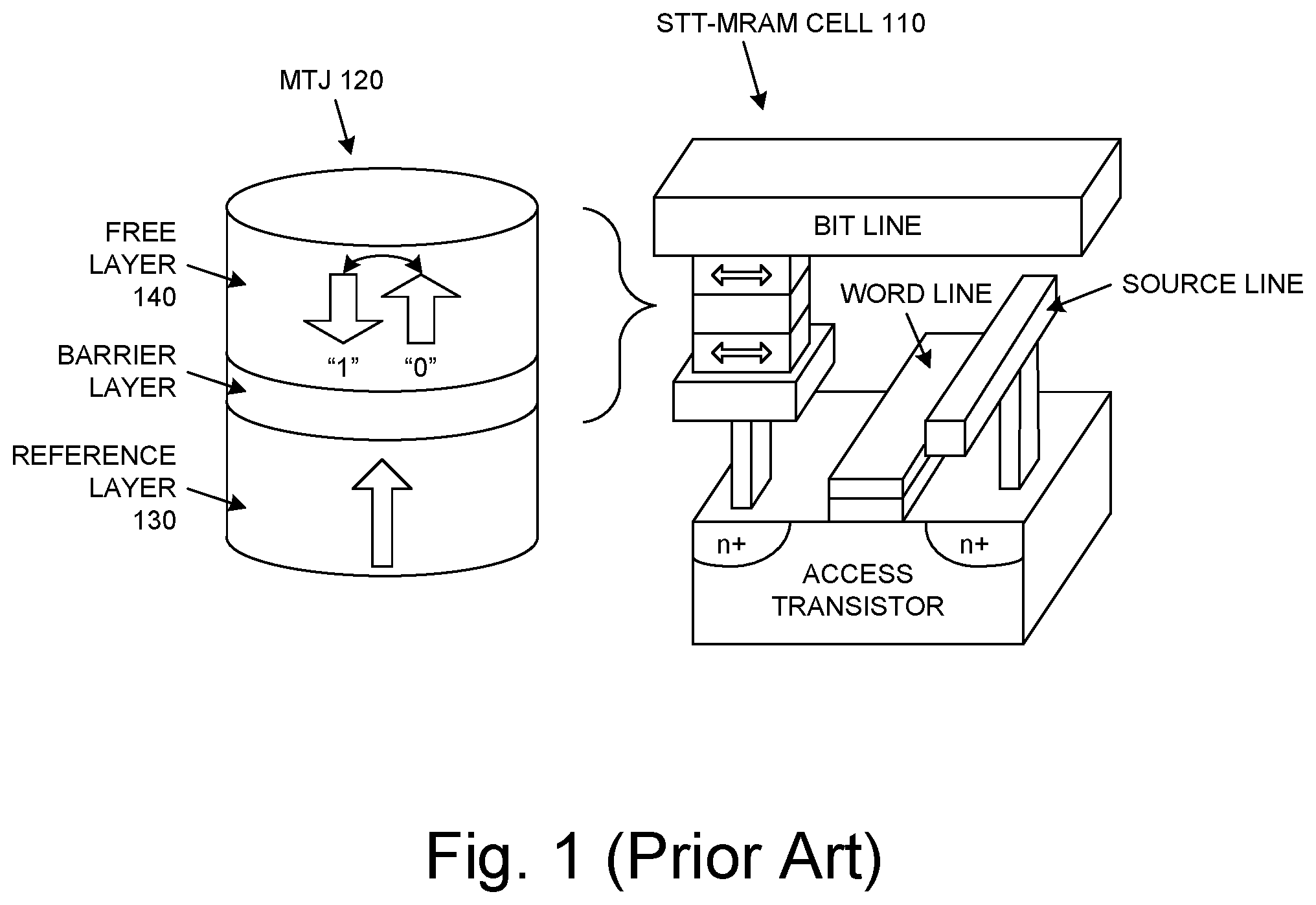
Magnetoresistive random access memory (MRAM) is a non-volatile memory technology that stores data through magnetic storage elements. The elements are two ferromagnetic plates or electrodes that can hold a magnetic field and are separated by a non-magnetic material, such as a non-magnetic metal or insulator. This structure is known as a magnetic tunnel junction (MTJ). MRAM devices are considered to be a next generation structure for a wide range of memory applications.
FIG. 1 illustrates an example of an MRAM cell 110 including an MTJ 120. In general, one of the plates (a reference layer or fixed layer 130) has its magnetization pinned, meaning that this layer has a higher coercivity than the other layer and requires a larger magnetic field or spin-polarized current to change the orientation of its magnetization. The second plate is typically referred to as the free layer 140 and its magnetization direction can be changed by a smaller magnetic field or spin-polarized current relative to that of the reference layer 130. The two plates can be sub-micron in lateral size, and the magnetization direction can still be stable with respect to thermal fluctuations.
MRAM devices can store information by changing the orientation of the magnetization of the free layer 140. In particular, based on whether the free layer 140 is in a parallel or anti-parallel alignment relative to the reference layer 130, either a binary value of "1" or a binary value of "0" can be stored in the MRAM cell 110 as represented in FIG. 1.
MRAM products based on spin transfer torque switching, or spin transfer switching, are already making their way into larger data storage devices. Spin transfer torque MRAM (STT-M RAM) devices, such as the one illustrated in FIG. 1, use spin-aligned (polarized) electrons to change the magnetization orientation of the free layer in the magnetic tunnel junction. In general, electrons possess a quantized number of angular momentum intrinsic to the electron referred to as spin. An electrical current is generally unpolarized; that is, it consists of 50% spin-up and 50% spin-down electrons. By passing a current though a magnetic layer, electrons are polarized with a spin orientation corresponding to the magnetization direction of the magnetic layer (e.g., polarizer), thereby producing a spin-polarized current. If the spin-polarized current is passed to the magnetic region of the free layer 140 in the MTJ device, the electrons will transfer a portion of their spin-angular momentum to the magnetization layer to produce a torque on the magnetization of the free layer. This spin transfer torque can switch the magnetization of the free layer 140, which in effect writes either a "1" or a "0" based on whether the free layer is in the parallel or anti-parallel state relative to the reference layer 130.
Due to the spin-polarized electron tunneling effect, the electrical resistance of the cell changes due to the orientation of the magnetic fields of the two layers 130 and 140. The electrical resistance is typically referred to as tunnel magnetoresistance (TMR), which is a magnetoresistance effect that occurs in an MTJ. The cell's resistance will be different for the parallel and anti-parallel states, and thus the cell's resistance can be used to distinguish between a "1" and a "0."
Generally speaking, to read a memory cell, a current is applied to the bit line that includes that cell (the "main bit line") to detect the value of the cell's resistance by monitoring the voltage across the cell. A sense amplifier is used to sense the voltage level on the main bit line and compare it to a reference bit line voltage. The reference bit line voltage is established at a level that is between the main bit line voltage that corresponds to a bit value of 1 and the main bit line voltage that corresponds to a bit value of 0. If the main bit line voltage is greater than the reference bit line voltage, then a "1" is stored in the cell; and if the main bit line voltage is less than the reference bit line voltage, then a "0" is stored in the cell.
There is a sense amplifier for each bit line. Thus, for example, for a 32-bit read, 32 sense amplifiers are used. Ideally, the sense amplifiers would be identical, but often there is a mismatch between them due to variations in circuit parameters deriving from manufacturing process, layout, position in the memory array, and location of the ground. These mismatches can result in erroneous reads.
This problem is illustrated by the example of FIGS. 2A and 2B. A reference bit line bias transistor 211 is connected to the reference bit line 201, and a main bit line bias transistor 212 is connected to the main bit line 202 of a memory cell being read. As illustrated in FIG. 2B, during the clock period of the sense amplifier 220, the reference bit line voltage supplied to the sense amplifier (Vs) is less than both the voltage (V1) that corresponds to a bit value of 1 and the voltage (V0) that corresponds to a bit value of 0 due to circuit parameter mismatch between the main bit line and the reference bit line. Thus, regardless of the actual bit value (0 or 1) stored by the memory cell that is being read, the sense amplifier 220 will sense a bit value of 1. That is, even if the actual stored bit value is 0, the sense amplifier 220 may erroneously sense a bit value of 1.
In an MTJ device, the difference between the main bit line voltage corresponding to a "1" and that corresponding to a "0" (the sensing margin) is small because the bit line resistance in series reduces the resistance ratio of the MTJs as seen by the sense amplifier. Also, a bias across an MTJ reduces the MTJ's resistance, especially the resistance of the anti-parallel state, and so TMR is reduced relative to the case of zero bias. Reduced TMR further decreases the sensing margin, which increases the possibility of an erroneous read. Thus, because of the relatively small sensing margin in MTJ devices, the problem of mismatches due to variations in circuit parameters and reference bit line voltage is particularly acute.
SUMMARY
Embodiments according to the present invention include a memory device that includes an array of memory cells, input/output lines (e.g., bit lines) coupled to the memory cells, and sense amplifiers coupled to the input/output lines. Each sense amplifier is associated with a respective input/output line. The device also includes trim circuits. Each trim circuit is associated with and coupled to a respective sense amplifier. Each sense amplifier receives a respective reference voltage that allows the sense amplifier to sense a bit value of an addressed memory cell. Each trim circuit is operable for independently compensating for variations in the reference voltage used by the respective sense amplifier.
In an embodiment, the memory cells include magnetoresistive random access memory (MRAM) cells, and the MRAM cells include magnetic tunnel junction (MTJ) memory cells.
In some embodiments, each trim circuit includes a number of transistors coupled to a ground and selectively coupled to a line that is coupled to a respective sense amplifier. In an embodiment, the trim circuit is coupled to a reference bit line that is coupled to the sense amplifier through a respective bit line bias transistor. In another embodiment, the trim circuit is coupled to a bit line bias line that is coupled to a respective bit line bias transistor that is coupled to a respective reference bit line that is coupled to the sense amplifier. In some of these embodiments, each trim circuit also includes a selection circuit that is coupled to the transistors and that is operable for selectively coupling one or more of the transistors to the line and for selectively decoupling one or more of the transistors from the line. In an embodiment, the transistors in the trim circuits have sizes that differ from each other by a factor of two.
In other embodiments, each trim circuit includes a variable resistor that is coupled to a supply voltage and that is also coupled to a reference bit line that is coupled to a respective sense amplifier.
Embodiments according to the present invention also include a method for configuring a trim circuit in a memory array. For each sense amplifier coupled to the memory array, a variation in an associated reference bit line voltage that places the associated reference bit line voltage outside a range of voltage values is detected; a respective program value to configure the respective programmable trim circuit to compensate for the variation is determined; and the respective program value is stored. When the program value is applied to configure a respective trim circuit, the associated reference bit line voltage is compensated so that it is within the range of voltage values. For example, the program value can be used to select (enable or disable) a number of transistors in a trim circuit or to select an amount of resistance in a trim circuit coupled to the sense amplifier.
In summary, embodiments according to the present invention use a trim circuit per sense amplifier to compensate for variations in the respective reference bit line voltage supplied to the sense amplifier. As a result, the reference bit line voltage supplied to each sense amplifier is maintained between the voltage associated with a bit value of 1 and the voltage associated with a bit value of 0. Mismatches between sense amplifiers are thereby compensated for or precluded. Consequently, the accuracy and reliability of read operations are increased. Specifically, erroneous reads due to mismatches in circuit parameters and variations in the reference bit line voltages are reduced in number if not completely eliminated, even when the sensing margin is small as it is for MTJ devices in MRAM arrays.
These and other objects and advantages of the various embodiments of the present invention will be recognized by those of ordinary skill in the art after reading the following detailed description of the embodiments that are illustrated in the various drawing figures.
BRIEF DESCRIPTION OF DRAWINGS
The accompanying drawings, which are incorporated in and form a part of this specification and in which like numerals depict like elements, illustrate embodiments of the present disclosure and, together with the detailed description, serve to explain the principles of the disclosure.
FIG. 1 illustrates an example of a conventional magnetoresistive random access memory cell.
FIG. 2A illustrates an example of a conventional memory device including a sense amplifier coupled to a reference bit line and to a main bit line.
FIG. 2B illustrates an example of voltages versus time for an erroneous read operation in a conventional memory device.
FIG. 3A illustrates a memory array in a memory device in embodiments according to the present invention.
FIG. 3B illustrates an example of voltages versus time for a read operation in embodiments according to the present invention.
FIG. 4 illustrates an embodiment of a trim circuit according to the present invention.
FIG. 5 illustrates a trim circuit coupled to a reference bit line in embodiments according to the present invention.
FIG. 6 illustrates a trim circuit coupled to a bit line bias line in embodiments according to the present invention.
FIG. 7 illustrates another embodiment of a trim circuit according to the present invention.
FIG. 8 is a flowchart of examples of operations in a method for configuring a trim circuit in embodiments according to the present invention.
FIG. 9 is an example of a computing system upon which embodiments according to the present invention can be implemented.
DETAILED DESCRIPTION
Reference will now be made in detail to the various embodiments of the present disclosure, examples of which are illustrated in the accompanying drawings. While described in conjunction with these embodiments, it will be understood that they are not intended to limit the disclosure to these embodiments. On the contrary, the disclosure is intended to cover alternatives, modifications and equivalents, which may be included within the spirit and scope of the disclosure as defined by the appended claims. Furthermore, in the following detailed description of the present disclosure, numerous specific details are set forth in order to provide a thorough understanding of the present disclosure. However, it will be understood that the present disclosure may be practiced without these specific details. In other instances, well-known methods, procedures, components, and circuits have not been described in detail so as not to unnecessarily obscure aspects of the present disclosure.
Some portions of the detailed descriptions that follow are presented in terms of procedures, logic blocks, processing, and other symbolic representations of operations on data bits within a computer memory. These descriptions and representations are the means used by those skilled in the data processing arts to most effectively convey the substance of their work to others skilled in the art. In the present application, a procedure, logic block, process, or the like, is conceived to be a self-consistent sequence of steps or instructions leading to a desired result. The steps are those utilizing physical manipulations of physical quantities. Usually, although not necessarily, these quantities take the form of electrical or magnetic signals capable of being stored, transferred, combined, compared, and otherwise manipulated in a computing system. It has proven convenient at times, principally for reasons of common usage, to refer to these signals as transactions, bits, values, elements, symbols, characters, samples, pixels, or the like.
It should be borne in mind, however, that all of these and similar terms are to be associated with the appropriate physical quantities and are merely convenient labels applied to these quantities. Unless specifically stated otherwise as apparent from the following discussions, it is appreciated that throughout the present disclosure, discussions utilizing terms such as "reading," "programming," "detecting," "determining," "storing," "applying," or the like, refer to actions and processes (e.g., the flowchart 800 of FIG. 8) of a computing system or similar electronic computing device or hardware processor (e.g., the system 900 of FIG. 9). The computing system or similar electronic computing device manipulates and transforms data represented as physical (electronic) quantities within the computing system memories, registers or other such information storage, transmission or display devices.
Memory Array with Individually Trimmable Sense Amplifiers
FIG. 3A illustrates a memory array 301 in a memory device 300 in embodiments according to the present invention. In embodiments, the memory device 300 is a magnetoresistive random access memory (MRAM) device. In an embodiment, the memory device 300 is a spin transfer torque (STT-MRAM) device.
The memory array 301 includes a number of memory cells or storage elements exemplified by the memory cell 302. As just noted, the memory cell 302 may be an MRAM cell. In embodiments, an MRAM cell includes a magnetic tunnel junction (MTJ).
The memory device 300 includes a number of word lines exemplified by the word lines WL(0), WL(1), . . . , WL(n), a number of bit lines exemplified by BL(0), BL(1), . . . , BL(m), and a number of source lines exemplified by SL(0), SL1(1), . . . , SL(m). Not all memory cells, word lines, bit lines, and source lines are shown in the figure. The bit lines may also be referred to herein as input/output lines.
The memory cell 302 is at the intersection of a particular word line, bit line, and source line. The memory cell 302 is individually addressable using a row address, which specifies the particular word line, and a column address, which specifies the particular bit line. The memory device 300 includes an x-decoder block 304 that decodes a row address signal and supplies a signal to the corresponding word line. The memory device 300 also includes a number of y-multiplexers (y-muxes) exemplified by the y-mux 306. The y-muxes provide column select logic for selecting a bit line and source line corresponding to a column address signal. A number of memory cells are typically addressed together to form a data word.
The memory device 300 also includes a number of sense amplifiers 310-0, 310-1, . . . , 310-N, collectively referred to herein as the sense amplifiers 310. Each of the sense amplifiers 310 is coupled to a respective set of the input/output lines (set of bit lines) through a respective y-mux as shown in FIG. 3A. Each sense amplifier can receive a voltage from a respective input/output line (bit line), specifically an input/output line (bit line) corresponding to the memory cell being read (the addressed memory cell). The voltage has a first level if a bit value of the addressed memory cell has a first binary value, and has a second level if the bit value of the addressed memory cell has a second binary value. Each sense amplifier also can receive a respective reference bit line voltage that allows the sense amplifier to sense the bit value of the addressed memory cell. Each sense amplifier 0, 1, N outputs a respective output (I/O) value (bit value) I/O 0, I/O 1, . . . , I/O N.
Significantly, in embodiments according to the present invention, the memory device 300 also includes a number of circuits 320-0, 320-1, . . . , 320-N collectively referred to herein as trim circuits 320. Each of the trim circuits 320 is associated with and coupled to a respective one of the sense amplifiers 310. That is, there is a different trim circuit for each sense amplifier.
As described further below, each of the trim circuits 320 compensates for variations in the respective bit line reference voltage received by the corresponding one of the sense amplifiers 310. That is, the trim circuits 320 are operable to individually correct variations in the reference bit line voltages respectively supplied to the sense amplifiers 310, and each trim circuit is operable to maintain the respective reference bit line voltage between a first voltage level (the voltage level associated with a bit value of 1) and a second voltage level (the voltage level associated with a bit value of 0), as shown in FIG. 3B.
FIG. 3B illustrates an example of voltages versus time for a read operation in embodiments according to the present invention. For example, the trim circuit 320-N compensates for variations in the reference voltage received by the sense amplifier 310-N. As a result, during the clock period of the sense amplifier 310-N, there is no mismatch between the main and reference bit line voltages and the reference bit line voltage supplied to the sense amplifier (Vs) is between the voltage (V1) that corresponds to a bit value of 1 and the voltage (V0) that corresponds to a bit value of 0. Thus, the sense amplifier 310-N will sense the proper bit value.
Co-pending U.S. patent application Ser. No. 15/858,398, entitled "Multi-Port Random Access Memory," by Mourad El Baraji et al., is hereby incorporated by reference in its entirety. That application describes a multi-port memory device that can access two or more memory cells at the same time. Embodiments according to the present disclosure can be utilized with and/or in a multi-port memory device as disclosed in the referenced application.
FIG. 4 illustrates a trim circuit 400 in embodiments according to the present invention. In some embodiments, each of the trim circuits 320 of FIG. 3A is implemented using the trim circuit 400. In other embodiments, each of the trim circuits 320 is implemented using the trim circuit 700 of FIG. 7, described further below.
The transistor tree 404 of FIG. 4 includes a number of transistors 401-0, 401-1, . . . , 401-k, collectively referred to herein as the transistors 401. In an embodiment, the sizes of the transistors differ from each other by a factor of two. Thus, for example, the transistor 401-1 is twice the size of the transistor 401-0, the transistor 401-2 (not shown) is twice the size of the transistor 401-1, and so on.
The transistors 401 receive a reference voltage from a voltage bias generator 405. The transistors 401 are coupled to a selection circuit 402. In general, as described further in conjunction with FIGS. 5 and 6 below, the selection circuit 402 is operable for selectively coupling and decoupling one or more of the transistors 401 to and from a respective reference bit line.
In an embodiment, the selection circuit 402 of FIG. 4 includes a number of switches 403-0, 403-1, . . . , 403-k, collectively referred to herein as the switches 403. The switches 403 can be implemented as transistors. Each of the transistors 401 is coupled to a respective one of the switches 403. Each of the switches 403 is controlled by a respective program value or configuration bit. If the configuration bit has a first binary value, then the switch is closed (enabled), and the switch is opened (disabled) if the configuration bit has a second binary value. Each of the transistors 401 is also coupled to a respective ground.
When a transistor in the transistor tree 404 is coupled to a respective reference bit line or respective bit line bias line (see FIGS. 5 and 6) by closing the associated one of the switches 403, a corresponding amount of current is trimmed (drained) from that line through the transistor to ground. As noted above, one or more of the transistors may be coupled to the line at a time. As described above, in an embodiment, the transistors 401 have different sizes. Thus, the amount of the trimmed current can be finely controlled by selecting a single one of the transistors (a single desired size) or any combination of the transistors (any desired combination of sizes).
In general, the program values used to configure the trim circuit 400 (FIG. 4) are determined by measuring the reference bit line voltage respectively supplied to each of the sense amplifiers 320 (FIG. 3A) and then determining the program values that will cause each respective reference bit line voltage to be in the range between the voltage for a binary value of 1 and the voltage for a binary value of 0. Ideally, each reference bit line voltage supplied to a sense amplifier is at about the midpoint of that range.
The program values used to control the switches 403 (FIG. 4) can be determined, for example, when the memory device 300 (FIG. 3A) is manufactured, and/or when the memory device is installed in a computing system, and/or each time the memory device is powered up. Alternatively, after installation, testing of the memory device 300 can be periodically performed and the program values can be determined accordingly.
Because a respective trim circuit is coupled to each sense amplifier, each trim circuit can be individually tuned. That is, the program values can be different for each of the trim circuits 400 of FIG. 4. Thus, the reference bit line voltage for each of the sense amplifiers 320 (FIG. 3A) can be individually trimmed, as opposed to global trimming of all sense amplifiers.
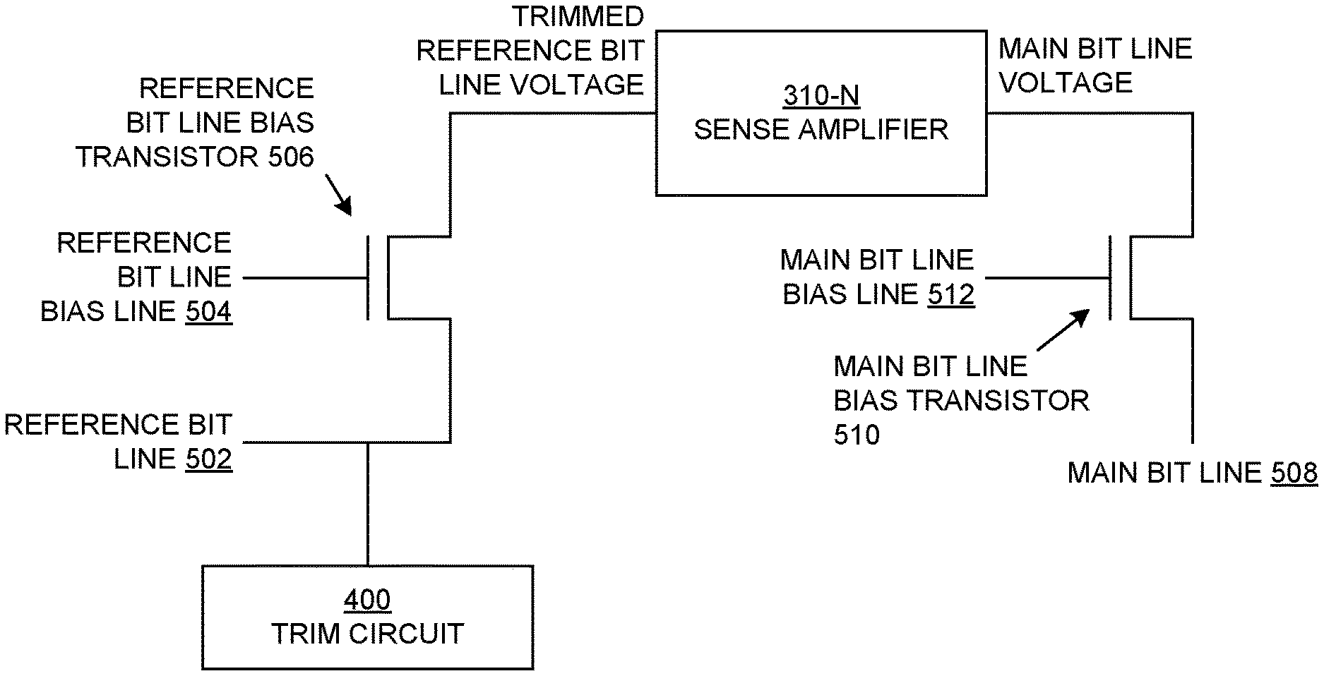
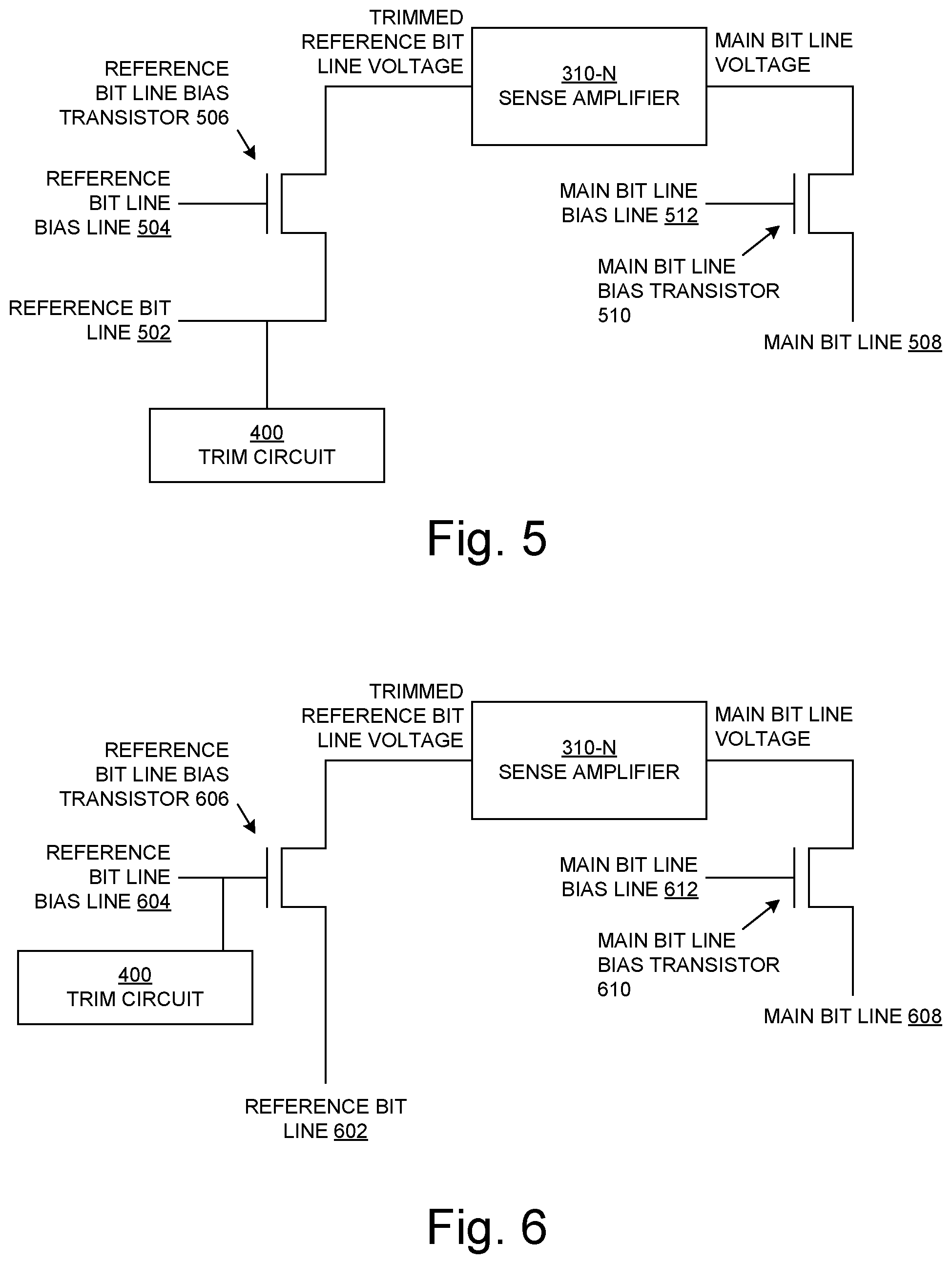
FIG. 5 illustrates a trim circuit 400 coupled to a reference bit line 502 in an embodiment according to the present invention. The sense amplifier 310-N is coupled to receive a reference bit line voltage from the reference bit line 502, which is connected to the sense amplifier through a reference bit line bias transistor 506. A reference bit line bias line 504 is connected to the gate of the reference bit line bias transistor 506. As described above, the trim circuit 400 is configured to trim a selected amount of current on the reference bit line 502 to compensate for variations in the reference bit line, so that a trimmed reference bit line voltage is supplied to the sense amplifier 310-N.
The sense amplifier 310-N is also coupled to receive a main bit line voltage from the main bit line 508, which is connected to the sense amplifier through a main bit line bias transistor 510. A main bit line bias line 512 is connected to the gate of the main bit line bias transistor 510. The main bit line voltage is the voltage on the bit line of the memory cell being read (the addressed memory cell). The sense amplifier 310-N can compare the main bit line voltage and the trimmed reference bit line voltage to determine the bit value of the memory cell being read.
FIG. 6 illustrates a trim circuit 400 coupled to a bit line bias line 604 in an embodiment according to the present invention. A reference bit line bias line 604 is connected to the gate of the reference bit line bias transistor 606 that is coupled to the reference bit line 602, which is coupled to the sense amplifier 310-N. As described above, the trim circuit 400 is configured to trim a selected amount of the current on the reference bit line bias line 604 to compensate for variations in the reference bit line 602, so that a trimmed reference bit line voltage is supplied to the sense amplifier 310-N. More specifically, the float on the reference bit line bias transistor 606 is adjusted to provide a different bias for the reference bit line 602 and trim the reference bit line voltage supplied to the sense amplifier 310-N.
The sense amplifier 310-N is also coupled to receive a main bit line voltage from the main bit line 608, which is connected to the sense amplifier through a main bit line bias transistor 610. A main bit line bias line 612 is connected to the gate of the main bit line bias transistor 610. The main bit line voltage is the voltage on the bit line of the memory cell being read (the addressed memory cell). The sense amplifier 310-N can compare the main bit line voltage and the trimmed reference bit line voltage to determine the bit value of the memory cell being read.
FIG. 7 illustrates a trim circuit 700 in another embodiment according to the present invention. As mentioned above, in some embodiments, each of the trim circuits 320 of FIG. 3A is implemented using the trim circuit 700. The trim circuit 700 includes a variable resistor 702 coupled to the reference bit line 704 and to supply voltage Vdd. The trim circuit 700 also includes a resistor 703 coupled between the supply voltage Vdd and the main bit line 710. The current on the reference bit line 702 can be trimmed using the trim circuit 700, by varying the resistances of the variable resistor 702, so that a trimmed reference bit line voltage is supplied to the sense amplifier 310-N.
The reference bit line 704 is coupled to the trim circuit 700 and to the sense amplifier 310-N through a reference bit line bias transistor 706. A reference bit line bias line 708 is connected to the gate of the reference bit line bias transistor 706.
The variable resistor 702 can be implemented using a digital potentiometer, or digitally controlled variable resistor, that is controlled by program values or configuration bits in a manner similar to that described above for the trim circuit 400. The program values used to control the variable resistor 702 can be determined, for example, when the memory device 300 (FIG. 3A) is manufactured, and/or when the memory device is installed in a computing system, and/or each time the memory device is powered up. Alternatively, after installation, testing of the memory device 300 can be periodically performed and the program values can be determined accordingly.
The sense amplifier 310-N is also coupled to receive a main bit line voltage from the main bit line 710, which is connected to the sense amplifier through a main bit line bias transistor 712. A main bit line bias line 714 is connected to the gate of the main bit line bias transistor 712. The main bit line 710 is also coupled to the trim circuit 700. The main bit line voltage is the voltage on the bit line of the memory cell being read (the addressed memory cell). The sense amplifier 310-N can compare the main bit line voltage and the trimmed reference bit line voltage to determine the bit value of the memory cell being read.
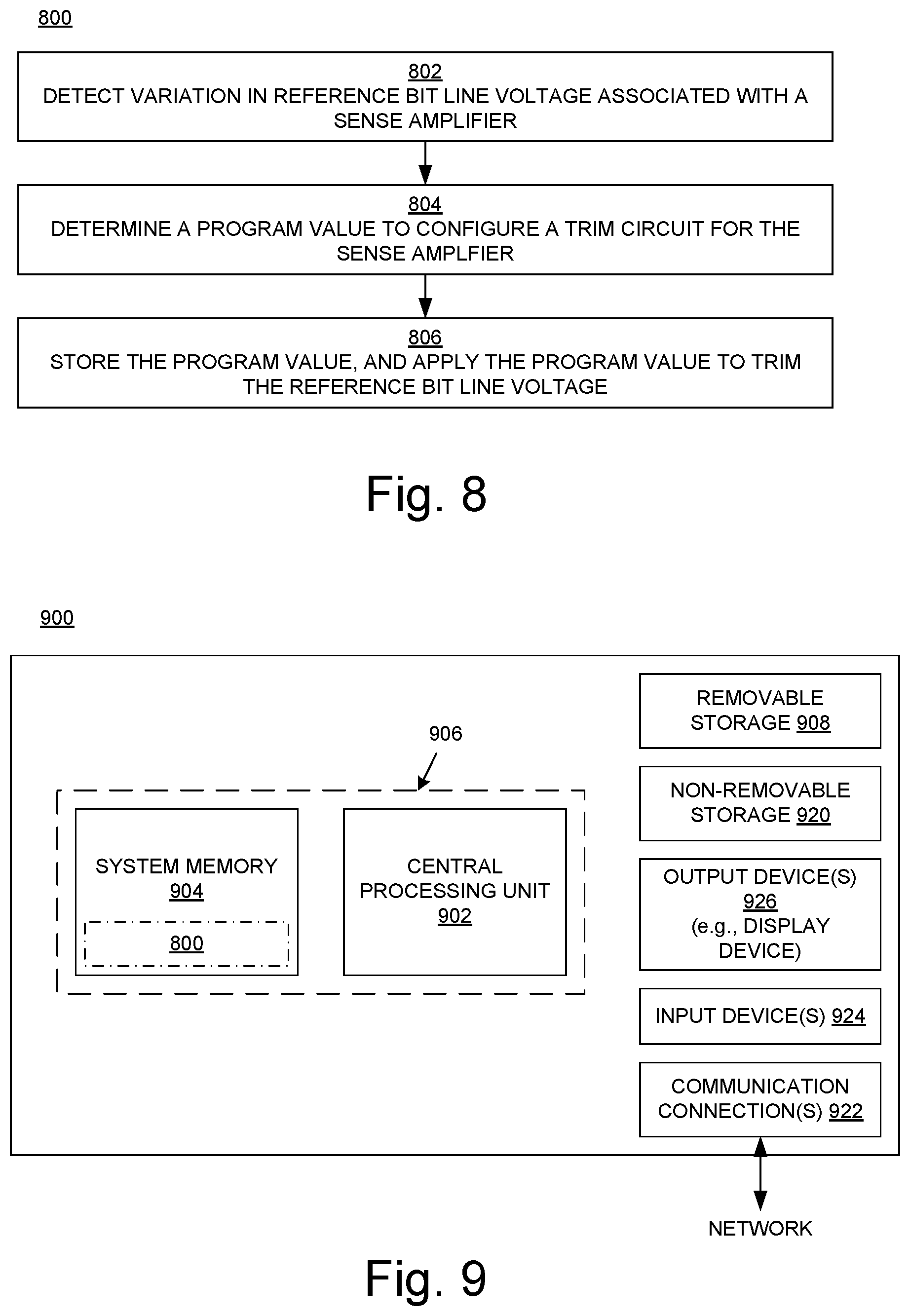
FIG. 8 is a flowchart 800 of examples of operations in a method for configuring a trim circuit in embodiments according to the present invention. The operations can be performed in and by the computing system 900 of FIG. 9. The computing system 900 can include the memory device 300 of FIG. 3A or can be coupled to the memory device. The operations in the flowchart 800 can be performed, for example, by a tester system when the memory device 300 is manufactured, and/or when the memory device is installed, and/or each time the memory device is powered up, and/or each time the memory device is tested. The operations in the flowchart 800 can be performed for each of the sense amplifiers 310 of FIG. 3A.
In block 802 of FIG. 8, a variation of a reference bit line voltage associated with a sense amplifier, that places the associated reference bit line voltage outside a range of voltage values, is detected.
In block 804, a respective program value or configuration bit to configure a respective programmable trim circuit (e.g., the trim circuit 400 or the trim circuit 700 of FIGS. 4 and 7, respectively) to compensate for the variation is determined.
In block 806, the respective program value is non-volatilely stored. The respective program value, when applied to configure the respective programmable trim circuit, causes the associated reference bit line voltage to be within the range of voltage values.
For implementations using the trim circuit 400 of FIG. 4 implemented as shown in FIG. 5, the respective program value is applied to select a number of transistors to be coupled to a reference bit line coupled to the respective sense amplifier through a respective bit line bias transistor. For implementations using the trim circuit 400 of FIG. 4 implemented as shown in FIG. 6, the respective program value is applied to select a number of transistors to be coupled to a bit line bias line coupled to a respective bit line bias transistor coupled to a respective reference bit line that is coupled to the respective sense amplifier.
For implementations using the trim circuit 700 of FIG. 7, the respective program value is applied to select an amount of resistance to be applied to a reference bit line coupled to the respective sense amplifier.
FIG. 9 is an example of a computing system 900 upon which embodiments according to the present invention can be implemented. In its most basic configuration, the system 900 includes at least one processing unit 902 and memory 904. This most basic configuration is illustrated in FIG. 9 by dashed line 906. The system 900 may also have additional features and/or functionality. For example, the system 900 may also include additional storage (removable and/or non-removable) including, but not limited to, magnetic or optical disks or tape. Such additional storage is illustrated in FIG. 9 by removable storage 908 and non-removable storage 920. The system 900 may also contain communications connection(s) 922 that allow the device to communicate with other devices, e.g., in a networked environment using logical connections to one or more remote computers.
The system 900 can also include input device(s) 924 such as keyboard, mouse, pen, voice input device, touch input device, etc. Output device(s) 926 such as a display device, speakers, printer, etc., are also included.
In the example of FIG. 9, the memory 904 includes computer-readable instructions, data structures, program modules, and the like associated with an application for executing a method for configuring a trim circuit in embodiments according to the present invention (e.g., the method of FIG. 8). For example, in an embodiment, the system 900 can include a tester system that can be connected to a memory device that includes a trim circuit (e.g., the memory device 300 of FIG. 3).
Thus, in embodiments according to the present invention, a trim circuit per sense amplifier is used to compensate for variations in the respective reference bit line voltage supplied to the sense amplifier. As a result, the reference bit line voltage supplied to each sense amplifier is maintained between the voltage associated with a bit value of 1 and the voltage associated with a bit value of 0. Mismatches between sense amplifiers are thereby compensated for or precluded. Consequently, the accuracy and reliability of read operations are increased. Specifically, erroneous reads due to mismatches in circuit parameters and variations in the reference bit line voltages are reduced in number if not completely eliminated, even when the sensing margin is small as it is for MTJ devices in MRAM arrays.
While the foregoing disclosure sets forth various embodiments using specific block diagrams, flowcharts, and examples, each block diagram component, flowchart step, operation, and/or component described and/or illustrated herein may be implemented, individually and/or collectively, using a wide range of hardware, software, or firmware (or any combination thereof) configurations. In addition, any disclosure of components contained within other components should be considered as examples because many other architectures can be implemented to achieve the same functionality.
The process parameters and sequence of steps described and/or illustrated herein are given by way of example only and can be varied as desired. For example, while the steps illustrated and/or described herein may be shown or discussed in a particular order, these steps do not necessarily need to be performed in the order illustrated or discussed. The example methods described and/or illustrated herein may also omit one or more of the steps described or illustrated herein or include additional steps in addition to those disclosed.
Although the subject matter has been described in language specific to structural features and/or methodological acts, it is to be understood that the subject matter defined in the disclosure is not necessarily limited to the specific features or acts described above. Rather, the specific features and acts described above are disclosed as example forms of implementing the disclosure.
Embodiments described herein may be discussed in the general context of computer-executable instructions residing on some form of computer-readable storage medium, such as program modules, executed by one or more computers or other devices. By way of example, and not limitation, computer-readable storage media may comprise non-transitory computer-readable storage media and communication media; non-transitory computer-readable media include all computer-readable media except for a transitory, propagating signal. Generally, program modules include routines, programs, objects, components, data structures, etc., that perform particular tasks or implement particular abstract data types. The functionality of the program modules may be combined or distributed as desired in various embodiments.
Computer storage media includes volatile and nonvolatile, removable and non-removable media implemented in any method or technology for storage of information such as computer-readable instructions, data structures, program modules or other data. Computer storage media includes, but is not limited to, random access memory (RAM), magnetoresistive random access memory (MRAM), read only memory (ROM), electrically erasable programmable ROM (EEPROM), flash memory or other memory technology, compact disk ROM (CD-ROM), digital versatile disks (DVDs) or other optical storage, magnetic cassettes, magnetic tape, magnetic disk storage or other magnetic storage devices, or any other medium that can be used to store the desired information and that can be accessed to retrieve that information.
Communication media can embody computer-executable instructions, data structures, and program modules, and includes any information delivery media. By way of example, and not limitation, communication media includes wired media such as a wired network or direct-wired connection, and wireless media such as acoustic, radio frequency (RF), infrared, and other wireless media. Combinations of any of the above can also be included within the scope of computer-readable media.
Embodiments according to the present invention are thus described. While the present invention has been described in particular embodiments, it should be appreciated that the present invention should not be construed as limited by such embodiments, but rather construed according to the following claims.
* * * * *
D00000
D00001
D00002
D00003
D00004
D00005
D00006
D00007
XML
uspto.report is an independent third-party trademark research tool that is not affiliated, endorsed, or sponsored by the United States Patent and Trademark Office (USPTO) or any other governmental organization. The information provided by uspto.report is based on publicly available data at the time of writing and is intended for informational purposes only.
While we strive to provide accurate and up-to-date information, we do not guarantee the accuracy, completeness, reliability, or suitability of the information displayed on this site. The use of this site is at your own risk. Any reliance you place on such information is therefore strictly at your own risk.
All official trademark data, including owner information, should be verified by visiting the official USPTO website at www.uspto.gov. This site is not intended to replace professional legal advice and should not be used as a substitute for consulting with a legal professional who is knowledgeable about trademark law.