Gated bipolar junction transistors, memory arrays, and methods of forming gated bipolar junction transistors
Gupta , et al. January 5, 2
U.S. patent number 10,886,273 [Application Number 16/436,689] was granted by the patent office on 2021-01-05 for gated bipolar junction transistors, memory arrays, and methods of forming gated bipolar junction transistors. This patent grant is currently assigned to Micron Technology, Inc.. The grantee listed for this patent is Micron Technology, Inc.. Invention is credited to Rajesh N. Gupta, Farid Nemati, Scott T. Robins.


View All Diagrams
| United States Patent | 10,886,273 |
| Gupta , et al. | January 5, 2021 |
Gated bipolar junction transistors, memory arrays, and methods of forming gated bipolar junction transistors
Abstract
Some embodiments include gated bipolar junction transistors. The transistors may include a base region between a collector region and an emitter region; with a B-C junction being at an interface of the base region and the collector region, and with a B-E junction being at an interface of the base region and the emitter region. The transistors may include material having a bandgap of at least 1.2 eV within one or more of the base, emitter and collector regions. The gated transistors may include a gate along the base region and spaced from the base region by dielectric material, with the gate not overlapping either the B-C junction or the B-E junction. Some embodiments include memory arrays containing gated bipolar junction transistors. Some embodiments include methods of forming gated bipolar junction transistors.
| Inventors: | Gupta; Rajesh N. (Karnataka, IN), Nemati; Farid (Redwood City, CA), Robins; Scott T. (San Jose, CA) | ||||||||||
|---|---|---|---|---|---|---|---|---|---|---|---|
| Applicant: |
|
||||||||||
| Assignee: | Micron Technology, Inc. (Boise,
ID) |
||||||||||
| Family ID: | 1000005284534 | ||||||||||
| Appl. No.: | 16/436,689 | ||||||||||
| Filed: | June 10, 2019 |
Prior Publication Data
| Document Identifier | Publication Date | |
|---|---|---|
| US 20190296016 A1 | Sep 26, 2019 | |
Related U.S. Patent Documents
| Application Number | Filing Date | Patent Number | Issue Date | ||
|---|---|---|---|---|---|
| 14613876 | Feb 4, 2015 | 10373956 | |||
| 13037642 | Feb 10, 2015 | 8952418 | |||
| Current U.S. Class: | 1/1 |
| Current CPC Class: | H01L 27/1026 (20130101); H01L 29/1608 (20130101); H01L 21/02381 (20130101); H01L 29/732 (20130101); H01L 29/7391 (20130101); H01L 29/73 (20130101); H01L 21/02529 (20130101); H01L 27/1024 (20130101); H01L 29/735 (20130101); H01L 21/8229 (20130101); H01L 27/1023 (20130101); H01L 27/10802 (20130101); H01L 2924/0002 (20130101); H01L 29/7841 (20130101); H01L 2924/0002 (20130101); H01L 2924/00 (20130101) |
| Current International Class: | H01L 21/8249 (20060101); H01L 27/102 (20060101); H01L 21/02 (20060101); H01L 29/739 (20060101); H01L 29/732 (20060101); H01L 29/16 (20060101); H01L 21/8229 (20060101); H01L 29/73 (20060101); H01L 29/735 (20060101); H01L 29/78 (20060101); H01L 27/108 (20060101) |
References Cited [Referenced By]
U.S. Patent Documents
| 3988771 | October 1976 | Krishna |
| 4487639 | December 1984 | Lam et al. |
| 5098861 | March 1992 | Blackstone |
| 5102821 | April 1992 | Moslehi |
| 5106776 | April 1992 | Shen et al. |
| 5260233 | November 1993 | Buti et al. |
| 5373184 | December 1994 | Moslehi |
| 5378316 | January 1995 | Franke et al. |
| 5412598 | May 1995 | Shulman |
| 5465249 | November 1995 | Cooper, Jr. et al. |
| 5471039 | November 1995 | Irwin, Jr. et al. |
| 5510630 | April 1996 | Agarwal et al. |
| 5563084 | October 1996 | Ramm et al. |
| 5600160 | February 1997 | Hvistendahl |
| 5874760 | February 1999 | Burns, Jr. et al. |
| 5904507 | May 1999 | Thomas |
| 5909618 | June 1999 | Forbes et al. |
| 5920105 | July 1999 | Okamoto et al. |
| 5930640 | July 1999 | Kenney |
| 5936274 | August 1999 | Forbes et al. |
| 5963469 | October 1999 | Forbes |
| 6017778 | January 2000 | Pezzani |
| 6033957 | March 2000 | Burns, Jr. et al. |
| 6137128 | October 2000 | Holmes et al. |
| 6191476 | February 2001 | Takahashi et al. |
| 6225151 | May 2001 | Gardner et al. |
| 6225165 | May 2001 | Noble, Jr. et al. |
| 6229161 | May 2001 | Nemati et al. |
| 6245663 | June 2001 | Zhao et al. |
| 6255731 | July 2001 | Ohmi et al. |
| 6274888 | August 2001 | Suzuki et al. |
| 6291836 | September 2001 | Kramer et al. |
| 6294418 | September 2001 | Noble |
| 6303468 | October 2001 | Aspar et al. |
| 6335231 | January 2002 | Yamazaki et al. |
| 6335258 | January 2002 | Aspar et al. |
| 6352894 | March 2002 | Goebel et al. |
| 6355501 | March 2002 | Fung et al. |
| 6355520 | March 2002 | Park et al. |
| 6365488 | April 2002 | Liao |
| 6391658 | May 2002 | Gates et al. |
| 6492662 | December 2002 | Hsu et al. |
| 6525953 | February 2003 | Johnson |
| 6559471 | May 2003 | Finder et al. |
| 6576944 | June 2003 | Weis |
| 6593624 | July 2003 | Walker |
| 6600173 | July 2003 | Tiwari |
| 6627924 | September 2003 | Hsu et al. |
| 6649980 | November 2003 | Noguchi |
| 6653174 | November 2003 | Cho et al. |
| 6690038 | February 2004 | Cho et al. |
| 6690039 | February 2004 | Nemati et al. |
| 6713791 | March 2004 | Hsu et al. |
| 6713810 | March 2004 | Bhattacharyya |
| 6727529 | April 2004 | Nemati et al. |
| 6744094 | June 2004 | Forbes |
| 6756286 | June 2004 | Moriceau et al. |
| 6764774 | July 2004 | Grill et al. |
| 6768156 | July 2004 | Bhattacharyya |
| 6777745 | August 2004 | Hshieh et al. |
| 6809044 | October 2004 | Aspar et al. |
| 6812504 | November 2004 | Bhattacharyya |
| 6815781 | November 2004 | Vyvoda et al. |
| 6841813 | January 2005 | Walker et al. |
| 6845034 | January 2005 | Bhattacharyya |
| 6870202 | March 2005 | Oka |
| 6881994 | April 2005 | Lee et al. |
| 6882008 | April 2005 | Ohsawa |
| 6888199 | May 2005 | Nowak et al. |
| 6891205 | May 2005 | Cho et al. |
| 6906354 | June 2005 | Hsu et al. |
| 6914286 | July 2005 | Park |
| 6934209 | August 2005 | Marr |
| 6940748 | September 2005 | Nejad et al. |
| 6940761 | September 2005 | Forbes |
| 6946365 | September 2005 | Aspar et al. |
| 6953953 | October 2005 | Horch |
| 6958263 | October 2005 | Bhattacharyya |
| 6958513 | October 2005 | Wang |
| 6965129 | November 2005 | Horch et al. |
| 6992349 | January 2006 | Lee et al. |
| 6995456 | February 2006 | Nowak |
| 7015092 | March 2006 | Jaiprakash et al. |
| 7029956 | April 2006 | Hsu et al. |
| 7052941 | May 2006 | Lee |
| 7075146 | July 2006 | Forbes |
| 7081663 | July 2006 | Bulucea |
| 7115939 | October 2006 | Forbes |
| 7120046 | October 2006 | Forbes |
| 7129538 | October 2006 | Lee |
| 7151024 | December 2006 | Forbes |
| 7157771 | January 2007 | Forbes |
| 7158401 | January 2007 | Bhattacharyya |
| RE39484 | February 2007 | Bruel |
| 7180135 | February 2007 | Ioannou |
| 7195959 | March 2007 | Plummer et al. |
| 7205185 | April 2007 | Dokumaci et al. |
| 7250628 | July 2007 | Bhattacharyya |
| 7250646 | July 2007 | Walker et al. |
| 7259415 | August 2007 | Forbes |
| 7268373 | September 2007 | Gupta et al. |
| 7271052 | September 2007 | Forbes |
| 7279740 | October 2007 | Bhattacharyya et al. |
| 7304327 | December 2007 | Hsu et al. |
| 7323380 | January 2008 | Forbes |
| 7326969 | February 2008 | Horch |
| 7338862 | March 2008 | Huo et al. |
| 7358120 | April 2008 | Furukawa et al. |
| 7359229 | April 2008 | Ferrant et al. |
| 7362609 | April 2008 | Harrison et al. |
| 7368352 | May 2008 | Kim et al. |
| 7378325 | May 2008 | Kaneko et al. |
| 7410867 | August 2008 | Forbes |
| 7415690 | August 2008 | Liang et al. |
| 7440310 | October 2008 | Bhattacharyya |
| 7456439 | November 2008 | Horch |
| 7476939 | January 2009 | Okhonin et al. |
| 7488627 | February 2009 | Nemati et al. |
| 7491608 | February 2009 | Forbes |
| 7518182 | April 2009 | Abbott et al. |
| 7525137 | April 2009 | Walker et al. |
| 7538000 | May 2009 | Dao |
| 7560336 | July 2009 | Abbott |
| 7579240 | August 2009 | Forbes |
| 7589995 | September 2009 | Tang et al. |
| 7592209 | September 2009 | Chang |
| 7615436 | November 2009 | Kouznetsov et al. |
| 7619917 | November 2009 | Nirschl et al. |
| 7629651 | December 2009 | Nakajima |
| 7663188 | February 2010 | Chung |
| 7736969 | June 2010 | Abbott et al. |
| 7786505 | August 2010 | Yang et al. |
| 7816728 | October 2010 | Ho et al. |
| 7825455 | November 2010 | Lee et al. |
| 7838360 | November 2010 | Forbes |
| 7851859 | December 2010 | Kyun et al. |
| 7883962 | February 2011 | Noble |
| 7897440 | March 2011 | Horch |
| 7929343 | April 2011 | Tang et al. |
| 8018058 | September 2011 | Lee |
| 8084316 | December 2011 | Huo et al. |
| 8102025 | January 2012 | Ozeki et al. |
| 8148780 | April 2012 | Tang et al. |
| 8476145 | July 2013 | Or-Bach et al. |
| 8501559 | August 2013 | Tang et al. |
| 8501581 | August 2013 | Tang et al. |
| 8507866 | August 2013 | Tang et al. |
| 8518812 | August 2013 | Mariani et al. |
| 8519431 | August 2013 | Nemati et al. |
| 8524543 | September 2013 | Tang |
| 8558220 | October 2013 | Schricker et al. |
| 8598621 | December 2013 | Tang |
| 8772848 | July 2014 | Zahurak |
| 9209187 | December 2015 | Mariani et al. |
| 9214389 | December 2015 | Righetti et al. |
| 9224738 | December 2015 | Zanderigo et al. |
| 2001/0002062 | May 2001 | Noble, Jr. et al. |
| 2001/0024841 | September 2001 | Noble, Jr. et al. |
| 2001/0026477 | October 2001 | Manning |
| 2001/0048119 | December 2001 | Mizuno et al. |
| 2002/0024152 | February 2002 | Momoi et al. |
| 2002/0028541 | March 2002 | Lee et al. |
| 2002/0070454 | June 2002 | Yasukawa |
| 2002/0079537 | June 2002 | Houston |
| 2002/0081753 | June 2002 | Gates et al. |
| 2002/0094619 | July 2002 | Mandelman et al. |
| 2002/0142562 | October 2002 | Chan et al. |
| 2002/0158254 | October 2002 | Hsu et al. |
| 2002/0163019 | November 2002 | Mohsen |
| 2002/0185684 | December 2002 | Campbell et al. |
| 2002/0190265 | December 2002 | Hsu et al. |
| 2002/0190298 | December 2002 | Alsmeier et al. |
| 2002/0195655 | December 2002 | Hshieh et al. |
| 2003/0006461 | January 2003 | Tezuka et al. |
| 2003/0102469 | June 2003 | Jones et al. |
| 2003/0164501 | September 2003 | Suzuki et al. |
| 2003/0186521 | October 2003 | Kub et al. |
| 2003/0211705 | November 2003 | Tong et al. |
| 2003/0223292 | December 2003 | Nejad et al. |
| 2003/0235710 | December 2003 | Grill et al. |
| 2004/0007717 | January 2004 | Yoo |
| 2004/0022105 | February 2004 | Ohsawa |
| 2004/0094758 | May 2004 | Usuda et al. |
| 2004/0097022 | May 2004 | Werkhoven |
| 2004/0130015 | July 2004 | Ogihara et al. |
| 2004/0159853 | August 2004 | Nemati et al. |
| 2004/0174734 | September 2004 | Forbes |
| 2004/0214379 | October 2004 | Lee et al. |
| 2004/0233761 | November 2004 | Schwabe et al. |
| 2004/0256639 | December 2004 | Ouyang |
| 2004/0262635 | December 2004 | Lee |
| 2004/0262679 | December 2004 | Ohsawa |
| 2005/0001232 | January 2005 | Bhattacharyya |
| 2005/0023656 | February 2005 | Leedy |
| 2005/0037582 | February 2005 | Dennard et al. |
| 2005/0059252 | March 2005 | Dokumaci et al. |
| 2005/0062079 | March 2005 | Wu et al. |
| 2005/0146955 | July 2005 | Kajiyama |
| 2005/0230356 | October 2005 | Empedocles et al. |
| 2005/0282318 | December 2005 | Dao |
| 2005/0282356 | December 2005 | Lee |
| 2006/0010056 | January 2006 | De La Motte |
| 2006/0034116 | February 2006 | Lam et al. |
| 2006/0071074 | April 2006 | Konevecki et al. |
| 2006/0082004 | April 2006 | Parekh et al. |
| 2006/0083058 | April 2006 | Ohsawa |
| 2006/0099776 | May 2006 | Dupont |
| 2006/0124974 | June 2006 | Cabral, Jr. et al. |
| 2006/0125011 | June 2006 | Chang |
| 2006/0197115 | September 2006 | Toda |
| 2006/0227601 | October 2006 | Bhattacharyya |
| 2006/0249770 | November 2006 | Huo et al. |
| 2007/0012945 | January 2007 | Sugizaki |
| 2007/0018166 | January 2007 | Atanackovic et al. |
| 2007/0018223 | January 2007 | Abbott |
| 2007/0023805 | February 2007 | Wells et al. |
| 2007/0023817 | February 2007 | Dao |
| 2007/0029607 | February 2007 | Kouznetzov |
| 2007/0045709 | March 2007 | Yang |
| 2007/0047364 | March 2007 | Chuang et al. |
| 2007/0051994 | March 2007 | Song et al. |
| 2007/0057328 | March 2007 | Taniguchi et al. |
| 2007/0064342 | March 2007 | Nakamura |
| 2007/0077694 | April 2007 | Lee |
| 2007/0080385 | April 2007 | Kim et al. |
| 2007/0121696 | May 2007 | Ishii |
| 2007/0127289 | June 2007 | Lee |
| 2007/0178649 | August 2007 | Swift et al. |
| 2007/0215954 | September 2007 | Mouli |
| 2007/0252175 | November 2007 | Tang et al. |
| 2007/0264771 | November 2007 | Ananthan et al. |
| 2008/0003774 | January 2008 | Baek |
| 2008/0003778 | January 2008 | Eyck |
| 2008/0041517 | February 2008 | Moriceau et al. |
| 2008/0124867 | May 2008 | Brown |
| 2008/0128802 | June 2008 | Huo et al. |
| 2008/0149984 | June 2008 | Chang et al. |
| 2008/0164528 | July 2008 | Cohen et al. |
| 2008/0200014 | August 2008 | Park et al. |
| 2008/0211023 | September 2008 | Shino |
| 2008/0211061 | September 2008 | Atwater, Jr. et al. |
| 2008/0233694 | September 2008 | Li |
| 2008/0237776 | October 2008 | Abbott |
| 2008/0246023 | October 2008 | Zeng et al. |
| 2008/0296712 | December 2008 | Feuillet |
| 2008/0299753 | December 2008 | Figura et al. |
| 2009/0003025 | January 2009 | Mokhlesi et al. |
| 2009/0010056 | January 2009 | Kuo et al. |
| 2009/0014813 | January 2009 | Chao et al. |
| 2009/0022003 | January 2009 | Song et al. |
| 2009/0026522 | January 2009 | Ananthan |
| 2009/0050948 | February 2009 | Ishikawa |
| 2009/0072341 | March 2009 | Liu et al. |
| 2009/0079030 | March 2009 | Cheng et al. |
| 2009/0108351 | April 2009 | Yang et al. |
| 2009/0129145 | May 2009 | Slesazeck |
| 2009/0140290 | June 2009 | Schulze et al. |
| 2009/0170261 | July 2009 | Lee |
| 2009/0173984 | July 2009 | Wang |
| 2009/0179262 | July 2009 | Holz |
| 2009/0189228 | July 2009 | Zhang et al. |
| 2009/0200536 | August 2009 | Van Schaijk et al. |
| 2009/0201723 | August 2009 | Okhonin et al. |
| 2009/0207681 | August 2009 | Juengling |
| 2009/0213648 | August 2009 | Slesazeck |
| 2009/0218656 | September 2009 | Gonzalez et al. |
| 2009/0242865 | October 2009 | Lung et al. |
| 2009/0246952 | October 2009 | Ishizaka et al. |
| 2009/0250738 | October 2009 | Dyer |
| 2009/0315084 | December 2009 | Cha et al. |
| 2010/0001271 | January 2010 | Fumitake |
| 2010/0006938 | January 2010 | Jang |
| 2010/0008139 | January 2010 | Bae |
| 2010/0044670 | February 2010 | Ling |
| 2010/0061145 | March 2010 | Weis |
| 2010/0197141 | August 2010 | Tu et al. |
| 2010/0200916 | August 2010 | Gossner et al. |
| 2010/0203695 | August 2010 | Oh et al. |
| 2010/0207180 | August 2010 | Lee |
| 2010/0248153 | September 2010 | Lee et al. |
| 2010/0277982 | November 2010 | Okhonin |
| 2011/0006377 | January 2011 | Lee et al. |
| 2011/0024791 | February 2011 | Schulze et al. |
| 2011/0121366 | May 2011 | Or-Bach et al. |
| 2011/0156044 | June 2011 | Lee et al. |
| 2011/0163357 | July 2011 | Tan et al. |
| 2011/0215371 | September 2011 | Tang et al. |
| 2011/0215396 | September 2011 | Tang et al. |
| 2011/0215407 | September 2011 | Tang et al. |
| 2011/0215408 | September 2011 | Tang et al. |
| 2011/0215436 | September 2011 | Tang et al. |
| 2011/0223725 | September 2011 | Kang et al. |
| 2011/0223731 | September 2011 | Chung et al. |
| 2011/0309434 | December 2011 | Huang et al. |
| 2012/0056194 | March 2012 | Dimitrijev |
| 2012/0205736 | August 2012 | Housley et al. |
| 2012/0223369 | September 2012 | Gupta et al. |
| 2012/0223380 | September 2012 | Lee et al. |
| 2014/0008721 | January 2014 | Filippini et al. |
| 2014/0106554 | April 2014 | Pozzi et al. |
| 2016/0049404 | February 2016 | Mariani et al. |
| 101405849 | Aug 2009 | CN | |||
| 101621036 | Jan 2010 | CN | |||
| 1494288 | Jan 2005 | EP | |||
| 1918998 | May 2008 | EP | |||
| H02-275663 | Nov 1990 | JP | |||
| H04-064249 | Feb 1992 | JP | |||
| H04-186815 | Jul 1992 | JP | |||
| H04-283914 | Oct 1992 | JP | |||
| 06-104446 | Apr 1994 | JP | |||
| H08-088153 | Apr 1996 | JP | |||
| H10-150176 | Jun 1998 | JP | |||
| H11-103035 | Apr 1999 | JP | |||
| 2000-150905 | May 2000 | JP | |||
| 2003-030980 | Jan 2003 | JP | |||
| 2004-303398 | Oct 2004 | JP | |||
| 2005-136191 | May 2005 | JP | |||
| 2005-327766 | Nov 2005 | JP | |||
| 2007-511895 | May 2007 | JP | |||
| 2008-010503 | Jan 2008 | JP | |||
| 2009-531860 | Sep 2009 | JP | |||
| 2011-508979 | Mar 2011 | JP | |||
| 10-0663359 | Oct 2006 | KR | |||
| 10-0702014 | Nov 2006 | KR | |||
| 10-0821456 | Apr 2008 | KR | |||
| 2009-0040460 | Apr 2009 | KR | |||
| 2009-0054245 | May 2009 | KR | |||
| 10-2010-0070835 | Jun 2010 | KR | |||
| 200802866 | Jan 2008 | TW | |||
| WO 2007/123609 | Nov 2007 | WO | |||
| WO 2009/088889 | Jul 2009 | WO | |||
Other References
|
CN 201180011589.X SR Trans., dated Aug. 21, 2014, Micron Technology, Inc. cited by applicant . CN 201180011589.X SR Trans., dated Apr. 10, 2015, Micron Technology, Inc. cited by applicant . CN 201180011628.6 SR Trans., dated Jun. 25, 2014, Micron Technology, Inc. cited by applicant . CN 201180011628.6 SR Trans., dated Feb. 27, 2015, Micron Technology, Inc. cited by applicant . CN 201180011630.3 SR Trans., Jul. 7, 2014, Micron Technology, Inc. cited by applicant . EP 11751050 Supp Search Report, dated Nov. 14, 2014, Micron Technology, Inc. cited by applicant . EP 11751053 Supp Search Report, dated Jun. 4, 2014, Micron Technology, Inc. cited by applicant . WO PCT/US2011/024354 IPRP, dated Sep. 4, 2012, Micron Technology, Inc. cited by applicant . WO PCT/US2011/024354 Search Report, dated Sep. 29, 2011, Micron Technology, Inc. cited by applicant . WO PCT/US2011/024354 Written Opinion, dated Sep. 29, 2011, Micron Technology, Inc. cited by applicant . WO PCT/US2011/024376 IPRP, dated Sep. 4, 2011, Micron Technology, Inc. cited by applicant . WO PCT/US2011/024376 Search Report, dated Sep. 28, 2011, Micron Technology, Inc. cited by applicant . WO PCT/US2011/204376 Written Opinion, dated Sep. 28, 2011, Micron Technology, Inc. cited by applicant . WO PCT/US2011/024387 IPRP, dated Sep. 4, 2012, Micron Technology, Inc. cited by applicant . WO PCT/US2011/024387 Search Report, Sep. 21, 2011, Micron Technology, Inc. cited by applicant . WO PCT/US2011/024387 Written Opinion, dated Sep. 21, 2011, Micron Technology, Inc. cited by applicant . WO PCT/US2012/021438 IPRP, dated Aug. 13, 2013, Micron Technology, Inc. cited by applicant . WO PCT/US2012/021438 Search Report, dated Aug. 28, 2012, Micron Technology, Inc. cited by applicant . WO PCT/US2012/021438 Written Opinion, dated Aug. 28, 2012, Micron Technology, Inc. cited by applicant . WO PCT/US2012/025109 IPRP, dated Sep. 10, 2013, Micron Technology, Inc. cited by applicant . WO PCT/US2012/025109 Search Report, dated Sep. 20, 2012, Micron Technology, Inc. cited by applicant . WO PCT/US2012/025109 Written Opinion, dated Sep. 20, 2012, Micron Technology, Inc. cited by applicant . WO PCT/US2012/025115 IPRP, dated Sep. 3, 2013, Micron Technology, Inc. cited by applicant . WO PCT/US2012/025115 Search Report, dated Sep. 24, 2012, Micron Technology, Inc. cited by applicant . WO PCT/US2012/025115 Written Opinion, Sep. 24, 2012, Micron Technology, Inc. cited by applicant . TW 100106775 Search Report Translation, dated Jun, 19, 2014, Micron Technology, Inc. cited by applicant . TW 100106776 Search Report Translation, dated Nov. 25, 2014, Micron Technology, Inc. cited by applicant . TW 100108777 SR Translation, Feb. 13, 2014, Micron Technology, Inc. cited by applicant . TW 101104088 SR Translation, dated Dec. 17, 2013, Micron Technology, Inc. cited by applicant . TW 101106601 SR Translation, dated Apr. 3, 2014, Micron Technology, Inc. cited by applicant . TW 101107759 SR Translation, dated Jun. 10, 2014, Micron Technology, Inc. cited by applicant . "IBM Builds World's Fastest Communications Microchip", Reuters U.S. Company News, Feb. 25, 2002, online at http://activequote300.fidelity.com/rtrnews/individua_n.../COMP&provider=C- BSMW%26toc_select%3Dmarket_breaking_news, 1 page. cited by applicant . Bae et al., "A Novel SiGe-Inserted SOI Structure for High Performance PDSOI CMOSFET", IEEE Electron Devices Meeting, 2000, United States, pp. 667-670. cited by applicant . Belford et al., Performance-Augmented CMOS Using Back-End Uniaxial Strain, Device Research Conference Digest, 2002, United States, pp. 41-42. cited by applicant . Bhattacharyya, "The Role of Microelectronic Integration in Environmental Control: A Perspective", Materials Research Society Symposium Proceedings vol. 344, 1994, United States, pp. 281-293. cited by applicant . Burke et al., "Silicon Carbide Thyristors for Power Applications", 10th IEEE International Pulsed Power Conference Digest of Technical Papers vol. 1, 1995, United States, pp. 327-335. cited by applicant . Cheng et al., "SiGe-on-Insulator (SGOI): Substrate Preparation and MOSFET Fabrication for Electron Mobility Evaluation (and conference outline)", IEEE International SOI Conference, Oct. 2001, United States, pp. 13-14 and 3 page outline. cited by applicant . Cheong et al., "Investigation of Ultralow Leakage in MOS Capacitors on 4H SiC", IEEE Transactions on Electron Devices, vol. 51(9), Sep. 2004, United States, pp. 1361-1365. cited by applicant . Cho et al., "A Novel Capacitor-Less DRAM Cell Using Thin Capacitively-Coupled Thyristor (TCCT)", IEEE, 2005, United States, 4 pages. cited by applicant . Current et al., "Atomic-Layer Cleaving with SixGey Strain Layers for Fabrication of Si and Ge-Rich SOI Device Layers", IEEE International SOI Conference, Oct. 2001, United States, pp. 11-12. cited by applicant . Dimitraiadis et al., "New a-SiC, Optically Controlled, Thyristor-Like Switch", Electronics Letters, vol. 28(17), Aug. 13, 1992, United Kingdom, pp. 1622-1624. cited by applicant . Ernst et al., "Fabrication of a Novel Strained SiGe:C-channel Planar 55 nm nMOSFET for High-Performance CMOS", Digest of Technical Papers--Symposium on VLSI Technology, 2002, United States, pp. 92-93. cited by applicant . Feder, "I.B.M. Finds Way to Speed Up Chips", The New York Times, Jun. 8, 2001, reprinted from http://www.nytimes.com/2001/06/08/technology/08BLUE.html, 2 pages. cited by applicant . Garone et al., "Mobility Enhancement and Quantum Mechanical Modeling in GexSi1-x Channel MOSFETs from 90 to 300K", IEEE Electron Devices Meetins, 1991, United States, pp. 29-32. cited by applicant . Gu et al., "High Performance Sub-100 nm Si Thin-Film Transistors by Pattern-Controlled Crystallization of Thin Channel Layer and High Temperature Annealing", Device Research Conference Digest, 2002, United States, pp. 49-50. cited by applicant . Hara et al., "High Performance Poly-Si TFTs on a Glass by a Stable Scanning CW Laser Lateral Crystallization", IEEE Electron Devices Meeting, 2001, United States, pp. 747-750. cited by applicant . Hara et al., "Selective Single-Crysralline-Silicon Growth at the Pre-Defined Active Regions of TFTs on a Glass by a Scanning CW Layer Irradiation", IEEE Electron Devices Meeting, 2000, United States, pp. 209-212. cited by applicant . Huang et al., "Carrier Mobility Enhancement in Strained SI-on-Insulator Fabricated by Wafer Bonding", Digest of Technical Papers--Symposium on VLSI Technology, 2001, United States, pp. 57-58. cited by applicant . Jager et al., "Single Grain Thin-Fim-Transistor (TFT) with SOI CMOS Performance Formed by Metal-Induced-Lateral-Crystallization", IEEE Electron Devices Meeting, 1999, United States, pp. 293-296. cited by applicant . Jen et al., "Electrical and Luminescent Characteristics of a-SIC:H P-I-N Thin-Film LED's with Graded-Gap Junctions", IEEE Transactions on Electron Devices, vol. 44(4), Apr. 1997, United States, pp. 565-571. cited by applicant . Jeon et al., "A New Poly-Si TFT with Selectively Doped Channel Fabricated by Novel Excimer Laser Annealing", IEEE Electron Devices Meeting, 2000, United States, pp. 213-216. cited by applicant . Kesan et al., "High Performance 0.25 .mu.m p-MOSFETs with Silicon-Germanium Channels for 300K and 77K Operation", IEEE Electron Devices Meeting, 1991, United States, pp. 25-28. cited by applicant . Kim et al., "A New High-Performance Poly-Si TFT by Simple Exclmer Laser Annealing on Selectively Floating a-Si Layer", IEEE Electron Devices Meeting, 2001, United States, pp. 751-754. cited by applicant . King et al, "A Low-Temperature (<550.degree.C) Silicon-Germanium MOS Thin-Film Transistor Technology for Large-Area Electronics", IEEE Electron Devices Meeting, 1991, United States, pp. 567-570. cited by applicant . Kuriyama et al., "High Mobility Poly-Si TFT by a New Excimer Laser Annealing Method for Large Area Electronics", IEEE Electron Devices Meeting, 1991, United States, pp. 563-566. cited by applicant . Li et al., "Design of High Speed Si/SiGe Heterojunction Complementary MOSFETs with Reduced Short-Channel Effects", National Central University, ChungLi, Taiwan, ROC, Aug. 2001, Contract No. NSC 89-2215-E-008-049, National Science Council of Taiwan, pp. 1 and 9. cited by applicant . Lu et al., "A Buried-Trench DRAM Cell Using a Self-Aligned Epitaxy Over Trench Technology", IEEE Electron Devices Meeting, 1988, United States, pp. 588-591. cited by applicant . Markoff, "I.B.M. Circuits are Now Faster and Reduce Use of Power", The New York Times, Feb. 25, 2002, reprinted Mar. 20, 2002, online http://story.news.yahoo.com/ news?tmpl=story&u=/nyt/200220225/.../i_b_m_circuits_are_now_faster_and_re- duce_use_of_power, 1 page. cited by applicant . Mizuno et al., "High Performance CMOS Operation of Strained-SOI MOSFETs Using Thin Film SiGe-on-Insulator Substrate", Digest of Technical Papers--Symposium on VLSI Technology, 2002, United States, pp. 106-107. cited by applicant . Myers et al., "Deuterium Interactions in Oxygen-Implanted Copper", Journal of Applied Physics vol. 65(1), Jan. 1, 1989, United States, pp. 311-321. cited by applicant . Nayfeh et al., "Electron Inversion Layer Mobility in Strained-Si n-MOSFET's with High Channel Doping Concentration Achieved by Ion Implantation", Device Research Conference Digest, 2002, United States, pp. 43-44. cited by applicant . Nemati et al., "A Novel High Density, Low Voltage SRAM Cell with a Vertical NDR Device", IEEE, 1998, United States, 2 pages. cited by applicant . Ono et al., "Analysis of Current-Voltage Characteristics in Polysilicon TFTs for LCDs". IEEE Electron Devices Meeting, 1988, United States, pp. 256-259. cited by applicant . Park et al., "Normal Incident SiGe/Si Multiple Quantum Well Infrared Detector", IEEE Electron Devices Meeting, 1991, United States, pp. 749-752. cited by applicant . Powell et al., "SiC Materials--Progress, Status, and Potential Roadblocks", Proceedings of the IEEE vol. 90(6), Jun. 2002, United States, pp. 942-955. cited by applicant . Rim et al., "Characteristics and Device Design of Sub-100 nm Strained SiN- and PMOSFETs", Digest of Technical Papers--Symposium on VLSI Technology, 2002, United States, pp. 98-99. cited by applicant . Rim et al., "Strained Si NMOSFET's for High Performance CMOS Technology", Digest of Technical Papers--Symposium on VLSI Technology, 2001, United States, pp. 59-60. cited by applicant . Saggio et al., "Innovative Localized Lifetime Control in High-Speed IGBT's", IEEE Electron Device Letters vol. 18, No. 7, Jul. 1997, United States, pp. 333-335. cited by applicant . Sasago et al., "Cross-point phase change memory with 4F2 cell size driven by low-contract-resistivity 1 poly-Si diode", Digest of Technical Papers--Symposium on VLSI Technology, 2009, United States, pp. 24-25. cited by applicant . Shima et al., "<100> Channel Strained-SiGe p-MOSFET with Enhanced Hole Mobility and Lower Parasitic Resistance", Digest of Technical Papers--Symposium on VLSI Technology, 2002, United States, pp. 94-95. cited by applicant . Sugizaki et al., "35-nm Gate-Length and Ultra Low-voltage (0.45 V) Operation Bulk Thyristor-SRAMIDRAM (BT-RAM) Cell with the Triple Selective Epitaxy Layers (TELs)", Digest of Technical Papers--Symposium on VLSI Technolgy, 2008, United States, 1 page (abstract). cited by applicant . Suliman et al., "Gate-Oxide Grown on the Sidewalls and Base of aU-Shaped Si Trench: Effects of the Oxide and Oxide/Si Interface Condition on the Properties of Vertical MOS Devices", Microelectronic Engineering vol. 72, 2004, Netherlands, pp. 247-252. cited by applicant . Takagi, "Strained-Si- and SiGe-on-Insulator (Strained SOI and SGOI) MOSFETs for High Performance/Low Power CMOS Application", Device Research Conference Digest, 2002, United States, pp. 37-40. cited by applicant . Tezuka et al., "High-Performance Strained Si-on-Insulator MOSFETs by Novel Fabrication Processes Utilizing Ge-Condensation Technique", Digest of Technical Papers--Symposium on VLSI Technology, 2002, United States, pp. 96-97. cited by applicant . Tzeng et al., "Dry Etching of Silicon Materials in SF6 Based Plasmas", Journal of The Electrochemical Society vol. 134, Issue 9, 1987, United States, pp. 2304-2309. cited by applicant . Van Meer et al., "Ultra-Thin Film Fully-Depleted SOI CMOS with Raised G/S/D Device Architecture for Sub-100 nm Applications", IEEE International SOI Conference, Oct. 2001, United States, pp. 45-46. cited by applicant . Xie et al., "A Vertically Integrated Bipolar Storage Cell in 6H Silicon Carbide for Nonvolatile Memory Applications", IEEE Electron Device Letters vol. 15(6), Jun. 1994, United States, pp. 212-214. cited by applicant . Yamada et al., "Spread Source/Drain (SSD) MOSFET Using Selective Silicon Growth for 64Mbit DRAMs", IEEE Electron Devices Meeting, 1989, United States, pp. 35-38. cited by applicant . Yamauchi et al., "Drastically Improved Performance in Poly-Si TFTs with Channel Dimensions Comparable to Grain Size", IEEE Electron Devices Meeting, 1989, United States, pp. 353-356. cited by applicant . Yang et al., "High Performance CMOS Fabricated on Hybrid Substrate with Different Crystal Orientations", IEEE Electron Devices Meeting, 2003, United States, pp. 453-456. cited by applicant . Yu et al., "Low-Temperature Titanium-Based Wafer Bonding", Journal of the Electrocheical Society vol. 154, No. 1, 2007, United States, pp. H20-H25. cited by applicant. |
Primary Examiner: Li; Meiya
Attorney, Agent or Firm: Wells St. John P.S.
Parent Case Text
RELATED PATENT DATA
This patent resulted from a divisional of U.S. patent application Ser. No. 14/613,876 which was filed Feb. 4, 2015, which is a divisional of U.S. patent application Ser. No. 13/037,642 which was filed Mar. 1, 2011, each of which is hereby incorporated by reference.
Claims
We claim:
1. A method of forming a memory array, comprising: forming a series of access lines; forming a series of bitlines; forming a plurality of gated bipolar junction transistors, individual gated bipolar junction transistors comprised by the plurality of gated bipolar junction transistors each being uniquely addressed through combinations containing a single bitline comprised by the series of bitlines and a single access line comprised by the series of access lines, each of the individual gated bipolar junction transistors being formed by a methodology comprising: forming a vertical transistor pillar having a pair of opposing sidewalls, the pair of opposing sidewalls including a first sidewall and a second sidewall, the vertical transistor pillar having a base region between a pair of emitter/collector regions, one of the pair of emitter/collector regions being a first emitter/collector region and the other being a second emitter/collector region, the first emitter/collector region interfacing the base region at a first junction and the second emitter/collector region interfacing the base region at a second junction, the first emitter/collector region being directly electrically coupled with the single bitline; forming a first depletion region disposed at an interface of the base region and the first emitter/collector region, and forming a second depletion region disposed at an interface of the base region and the second emitter/collector region, the first depletion region and the second depletion region each comprising a silicon carbide material having a bandgap greater than or equal to 1.2 eV at 300 K, a portion of the first emitter/collector region comprising a non-silicon carbide material, a portion of the second emitter/collector region comprising the non-silicon carbide material, and a portion of the base region comprising the non-silicon carbide material, the non-silicon carbide material having a narrow bandgap; and forming a gate along the base region of the vertical transistor pillar, the gate not vertically overlapping either of the first junction and the second junction; and forming a dielectric material extending along an entirety of a vertical height of each of the first sidewall and the second sidewall of the vertical transistor pillar, a portion of the dielectric material along the first depletion region comprising silicon, oxygen and nitrogen.
2. The memory array of claim 1, further comprising coupling all of the second emitter/collector regions with one another and with a common terminal.
3. The memory array of claim 1, wherein the series of access lines is a first series of access lines, and further comprising forming a second series of access lines, one of the access lines comprised by the second series of access lines being directly electrically coupled with the second emitter/collector region.
4. A method of forming a gated bipolar junction transistor, comprising: forming a plurality of vertical transistor pillars over a monocrystalline substrate, each individual vertical transistor pillar comprised by the plurality of vertical transistor pillars comprising, in ascending order over the substrate: a first region comprising a first narrow-bandgap material; a second region comprising a first wide-bandgap material having a bandgap of greater than or equal to 1.2 eV; a third region comprising a second narrow-bandgap material; a fourth region comprising a second wide-bandgap material having a bandgap of greater than or equal to 1.2 eV; and a fifth region comprising a third narrow-bandgap material; forming a dielectric regions along opposing sidewalls of each individual vertical transistor pillar; and forming gates extending along the opposing sidewalls of each individual vertical transistor pillar, the gates being directly against the dielectric regions and being formed along the third region without overlapping the second region and without overlapping the fourth region.
5. The method of claim 4, wherein the first wide-bandgap material comprises silicon carbide.
6. The method of claim 4, wherein the second wide-bandgap material comprises silicon carbide.
7. The method of claim 4, wherein the dielectric region comprises a passivation material in direct physical contact with the opposing sidewalls of each of the individual vertical transistor pillars.
8. The method of claim 7, wherein the passivation material comprises silicon, oxygen and nitrogen.
Description
TECHNICAL FIELD
Gated bipolar junction transistors, memory arrays, and methods of forming gated bipolar junction transistors.
BACKGROUND
Memory is one type of integrated circuitry, and is used in computer systems for storing data. Integrated memory is usually fabricated in one or more arrays of individual memory cells. The memory cells might be volatile, semi-volatile, or nonvolatile. Nonvolatile memory cells can store data for extended periods of time, and in some instances can store data in the absence of power. Non-volatile memory is conventionally specified to be memory having a retention time of at least about 10 years. Volatile memory dissipates, and is therefore refreshed/rewritten to maintain data storage. Volatile memory may have a retention time of milliseconds, or less.
The memory cells are configured to retain or store memory in at least two different selectable states. In a binary system, the states are considered as either a "0" or a "1". In other systems, at least some individual memory cells may be configured to store more than two levels or states of information.
Nonvolatile memory may be used in applications in which it is desired to retain data in the absence of power. Nonvolatile memory may also be used in applications in which power is a limited resource (such as in battery-operated devices) as an alternative to volatile memory because nonvolatile memory may have the advantage that it can conserve power relative to volatile memory. However, read/write characteristics of nonvolatile memory may be relatively slow in comparison to volatile memory, and/or nonvolatile memory may have limited endurance (for instance, nonvolatile memory may only function for about 10.sup.5 read/write cycles before failure). Thus, volatile memory is still often used, even in devices having limited reserves of power. It would be desirable to develop improved nonvolatile memory and/or improved semi-volatile memory. It would be further desirable to develop memory cells that are nonvolatile or semi-volatile, while having suitable read/write characteristics and endurance to replace conventional volatile memory in some applications.
Integrated circuitry fabrication continues to strive to produce smaller and denser integrated circuits. It can be desired to develop small-footprint memory cells in order to conserve the valuable real estate of an integrated circuit chip. For instance, it can be desired to develop memory cells that have a footprint of less than or equal to 4F.sup.2, where "F" is the minimum dimension of masking features utilized to form the memory cells.
It would be desirable to develop new memory cells which can be non-volatile or semi-volatile, and which have may have a footprint approaching 4F.sup.2.
BRIEF DESCRIPTION OF THE DRAWINGS
FIG. 1 is a diagrammatic cross-sectional view of an example embodiment memory cell.
FIG. 2 is a diagrammatic cross-sectional view of another example embodiment memory cell.
FIG. 3 is a diagrammatic cross-sectional view of another example embodiment memory cell.
FIG. 4 is a diagrammatic cross-sectional view of another example embodiment memory cell.
FIG. 5 is a diagrammatic schematic view of an example embodiment memory array comprising memory cells of the type shown in FIG. 1.
FIG. 6 diagrammatically illustrates an example embodiment operational arrangement for utilizing the memory array of FIG. 5.
FIG. 7 is a diagrammatic schematic view of another example embodiment memory array comprising memory cells of the type shown in FIG. 1.
FIG. 8 diagrammatically illustrates an example embodiment operational arrangement for utilizing the memory array of FIG. 7.
FIG. 9 is a diagrammatic schematic view of an example embodiment memory array comprising memory cells of the type shown in FIG. 2.
FIGS. 10 and 11 diagrammatically illustrate example embodiment operational arrangements for utilizing the memory array of FIG. 9.
FIG. 12 is a diagrammatic schematic view of another example embodiment memory array comprising memory cells of the type shown in FIG. 2.
FIGS. 13 and 14 diagrammatically illustrate example embodiment operational arrangements for utilizing the memory array of FIG. 12.
FIG. 15 is a diagrammatic cross-sectional view of another example embodiment memory cell.
FIG. 16 is a diagrammatic cross-sectional view of another example embodiment memory cell.
FIGS. 17 and 18 diagrammatically illustrate process stages of an example embodiment method for fabricating an array of memory cells.
DETAILED DESCRIPTION OF THE ILLUSTRATED EMBODIMENTS
Some embodiments include memory cells comprising one or more wide-bandgap materials; with a "wide-bandgap material" being a material having a bandgap measurably greater than the 1.12 eV bandgap of silicon at 300 K. In some embodiments, the wide-bandgap material may have a bandgap of 1.2 eV or greater. In some embodiments, the wide-bandgap material may have a bandgap of 2.3 eV or greater, and may, for example, comprise one or more forms of silicon carbide.
The memory cells may be gated bipolar junction transistors (BJTs), and may comprise electrically floating bodies. In some embodiments, the wide-bandgap material may be utilized in the floating bodies and/or in depletion regions adjacent the floating bodies. Such utilization of the wide-bandgap material may enable formation of random access memory (RAM) having longer retention time than conventional dynamic random access memory (DRAM), while also having suitably fast read/write characteristics to substitute for conventional DRAM in some applications. Additionally, or alternatively, the wide-bandgap material may enable formation of memory having retention times of several years, and thus may enable formation of nonvolatile memory. In some embodiments, the nonvolatile memory may have endurance approaching, or even exceeding, the endurance of conventional DRAM (such as endurance suitable to survive 10.sup.6 or more read/write cycles).
Example gated BJT memory cells are described with reference to FIGS. 1-4.
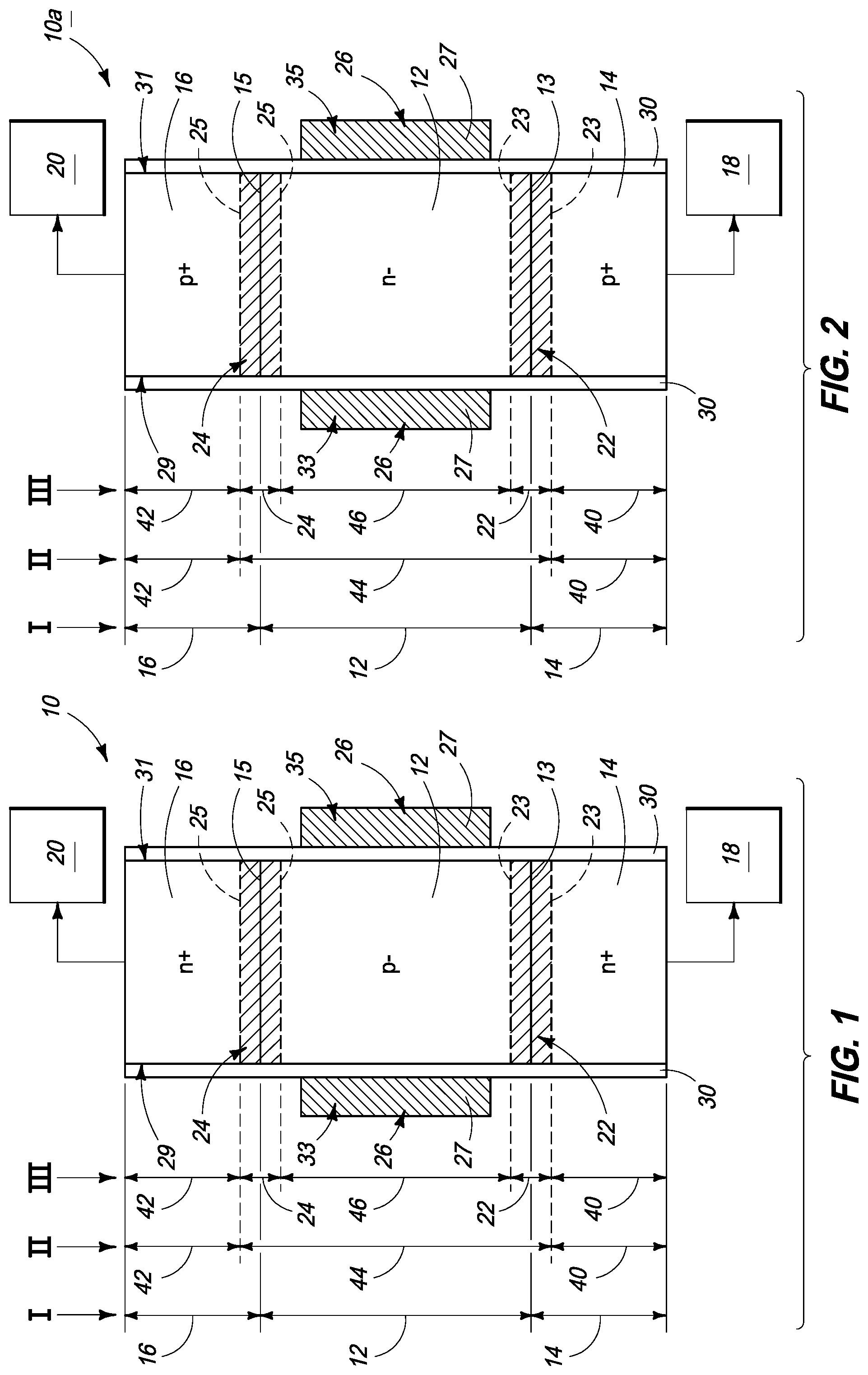
Referring to FIG. 1, a memory cell 10 comprises a base region 12 between a pair of emitter/collector regions 14 and 16. The regions 12, 14 and 16 may be comprised by a pillar-type structure in some embodiments, and such structure may be referred to as a BJT pillar.
The emitter/collector region 14 interfaces with the base region 12 at a junction 13, and similarly the emitter/collector region 16 interfaces with the base region 12 at a junction 15. In operation, one of the emitter/collector regions will be the emitter region of the BJT device, and the other will be the collector region of the device. The junction between the base region and the emitter region may be referred to as a B-E junction, and the junction between the base region and the collector region may be referred to as a B-C junction.
The emitter/collector regions 14 and 16 are shown to be electrically coupled to electrical nodes 18 and 20, respectively. One of the nodes 18 and 20 may correspond to a bitline (i.e., a digit line or sense line). The other of the nodes 18 and 20 may correspond to a wordline (i.e., an access line) in some embodiments, or to a ground or other electrically static structure in other embodiments.
The illustrated BJT of memory cell 10 has the base oppositely doped to the emitter/collector regions; and specifically comprises a p-type base and n-type emitter/collector regions. In other embodiments, the base region and emitter/collector regions may comprise other doping arrangements, as illustrated in FIGS. 2-4.
The symbols "+" and "-" are utilized in FIG. 1 (and various other figures of this disclosure) to indicate dopant levels. Some or all of the designations p+, p, p-, n-, n and n+ may be used to indicate various levels and types of doping. The difference in dopant concentration between the regions identified as being p+, p, and p- may vary depending on the particular material being doped. An example dopant concentration of a p+ region is a dopant concentration of at least about 10.sup.19 atoms/cm.sup.3 (and in some example applications may be from about 10.sup.19 atoms/cm.sup.3 to about 10.sup.20 atoms/cm.sup.3), an example dopant concentration of a p region is from about 10.sup.18 to about 10.sup.19 atoms/cm.sup.3, and an example dopant concentration of a p- region is less than about 5.times.10.sup.18 atoms/cm.sup.3 (and in some embodiments may be less than or equal to about 5.times.10.sup.17 atoms/cm.sup.3). The regions identified as being n-, n and n+ may have dopant concentrations similar to those described above relative to the p-, p and p+ regions, respectively.
It is noted that the terms "p" and "n" can be utilized herein to refer to both dopant type and relative dopant concentrations. The terms "p" and "n" are to be understood as referring only to dopant type, and not to a relative dopant concentration, except when it is explicitly stated that the terms refer to relative dopant concentrations. Accordingly, for purposes of interpreting this disclosure and the claims that follow, it is to be understood that the terms "p-type doped" and n-type doped" refer to dopant types of a region and not to relative dopant levels. Thus, a p-type doped region can be doped to any of the p+, p, and p- dopant levels discussed above, and similarly an n-type doped region can be doped to any of the n+, n, and n- dopant levels discussed above.
The dopants utilized in memory cell 10 may be any suitable dopants. In some embodiments, at least part of the memory cell will comprise wide-bandgap material. An example wide-bandgap material is silicon carbide, and such may be n-type doped with, for example, one or more of N (such as from N.sub.2 and/or NH.sub.3), P (such as from PH.sub.3) and As (such as from AsH.sub.3). Alternatively, the silicon carbide may be p-type doped with, for example, one or more of B (such as from B.sub.2H.sub.6), Al (such as from AlCl.sub.3, trimethylaluminum and triethylaluminum) and Ga (such as from trimethylgallium).
In operation, depletion regions 22 and 24 may be induced between base region 12 and the emitter/collector regions 14 and 16, respectively. The depletion regions are diagrammatically illustrated with cross-hatching. Approximate boundaries of the depletion region 22 are illustrated with dashed lines 23, and approximate boundaries of the depletion region 24 are illustrated with dashed lines 25.
The memory cell 10 has a gate 26 along the base region 12. In operation, the base region may comprise an electrically floating body of the memory cell. The gate may be used to enable charge to be selectively stored on such floating body, or to be drained from the floating body. Thus, the memory cell may have two selectable memory states, with one of the states having more charge stored on base region 12 than the other state.
The illustrated BJT is configured as a vertical pillar having a pair of opposing sidewalls 29 and 31, and the gate 26 is shown to be bifurcated into a pair of segments 33 and 35, with each segment being along one of the opposing sidewalls. In some embodiments, the illustrated memory cell may be one of a plurality of memory cells of a memory array, and the illustrated segments 33 and 35 of the gate may correspond to a pair of lines that extend along multiple memory cells of a row or column of the array to interconnect multiple memory cells. Such lines would extend in and out of the page relative to the cross-sectional view of FIG. 1. The segments 33 and 35 may join with one another at some location outside of the view of FIG. 1 so that the illustrated segments 33 and 35 are actually two parts of the same gate.
The gate 26 comprises a material 27. Such material may comprise any suitable substance, and may, for example, comprise one or more of various metals (for instance, titanium, tungsten, etc.), metal-containing compositions (for instance, metal silicide, metal nitride, etc.), and conductively-doped semiconductor materials (for instance, conductively-doped silicon, conducted-doped geranium, etc.).
The gate 26 is spaced from the sidewalls 29 and 31 of the BJT pillar by dielectric material 30. The dielectric material may comprise any suitable composition or combination of compositions. In some embodiments, at least a portion of the BJT pillar comprises one or more forms of silicon carbide, and at least a portion of the dielectric material 30 that is directly against the silicon carbide comprises a passivation composition containing silicon, oxygen and nitrogen. Such passivation composition may be formed by chemically reacting a surface of the silicon carbide with oxygen and nitrogen, and/or by depositing a composition containing silicon, oxygen and nitrogen along the surface of the silicon carbide.
In some embodiments, an entirety of dielectric material 30 may comprise the passivation composition containing silicon, oxygen and nitrogen. In other embodiments, the dielectric material 30 may comprise two or more different compositions, with the composition directly against surfaces of the BJT pillar being the passivation material, and with one or more other compositions being between the passivation material and the gate 26. Such other compositions may comprise, for example, one or both of silicon dioxide and silicon nitride.
In the shown embodiment, the gate 26 is along base region 12 of the BJT, but does not overlap the B-C and B-E junctions 13 and 15. Further, the gate does not overlap the depletion regions 22 and 24 during operation of the BJT. In the shown configuration in which the BJT is within a vertical pillar, the gate 26 may be considered to vertically overlap the base region, and to not vertically overlap the depletion regions 22 and 24.
It can be advantageous for gate 26 to not overlap depletion regions 22 and 24 in that such can alleviate or eliminate a source of leakage within the memory cell. Specifically, a gated BJT memory cell may have primary leakage mechanisms that include gate-induced leakage (which may be referred to as gate-induced-drain-leakage, i.e., GIDL), base/emitter junction leakage, and base/collector junction leakage. If the gate 26 overlaps the depletion regions, then a significant leakage mechanism within the memory cell may be gate-induced leakage, and such may be a much larger contribution to the leakage within the memory cell than the combination of intrinsic base/emitter junction leakage and intrinsic base/collector junction leakage. In the shown example embodiment of FIG. 1, the gate does not overlap the depletion regions, and thus only couples with the base region. Accordingly, the gate-induced leakage, if any, may be a small contribution to the overall leakage within the memory cell; and thus the overall leakage through the memory cell may be limited to the intrinsic leakage of the two junctions. This can enable the memory cell of FIG. 1 to have much longer retention times than conventional DRAM, and in some embodiments to have retention times suitable for utilization in nonvolatile memory.
The BJT pillar of memory cell 10 may be considered to be subdivided into numerous regions, as explained with reference to the scales I, II and III shown in FIG. 1.
Scale I illustrates that the BJT pillar may be considered to comprise a first emitter/collector region 14, a base region 12, and a second emitter/collector region 16. The regions 12 and 14 interface at the junction 13, and the regions 12 and 16 interface at the junction 15.
Scale II illustrates that the BJT pillar may be considered to comprise a first outer region 40 corresponding to the portion of the emitter/collector region 14 that is outward of the depletion region 22, a second outer region 42 corresponding to the portion of the emitter/collector region 16 that is outward of the depletion region 24, and an inner region 44 between the outer regions 40 and 42. The inner region 44 interfaces with outer region 40 at an outermost edge of depletion region 22, and interfaces with outer region 42 at an outermost edge of depletion region 24.
Scale III illustrates that the BJT pillar may be considered to comprise the outer regions 40 and 42, the depletion regions 22 and 24, and a neutral base region (or floating body region) 46 between the depletion regions.
As discussed above, the BJT pillar may comprise one or more wide-bandgap materials. The wide-bandgap materials may advantageously improve retention time of the memory cell relative to narrower-bandgap materials (such as silicon) by reducing leakage within the memory cell. In some embodiments, wide-bandgap material is provided at least across the junctions 13 and 15 in wide enough expanses to fully encompass depletion regions 22 and 24. Thus, the wide-bandgap material is provided across the locations where the wide-bandgap material may reduce base/collector junction leakage and base/emitter junction leakage. In some embodiments, the wide-bandgap material may be provided as strips extending across depletion regions 22 and 24, and thus the regions 40, 46 and 42 of scale III may be narrow-bandgap materials (such as silicon). In such embodiments, the wide-bandgap material across depletion region 22 may be the same composition as the wide-bandgap material across depletion region 24, or may be a different composition to tailor the BJT for a particular application of the memory cell 10.
Possible means by which the wide bandgap materials may reduce leakage within the BJT are as follows. Intrinsic leakage may be considered to be derived through two different mechanisms, and to approximately correspond to whichever of the mechanisms predominates. One of the mechanisms is generation of intrinsic carriers in depletion regions, and the other is diffusion of intrinsic carriers in the neutral regions. The concentration of intrinsic carriers (n.sub.i) may be represented by Equation I:
.times..times..times. ##EQU00001##
In Equation I, E.sub.g is the bandgap, T is temperature, and k is Boltzmann's constant. Intrinsic leakage will be approximately proportional to n.sub.i for a leakage mechanism corresponding to generation of intrinsic carriers in depletion regions, and will be approximately proportional to (n.sub.i).sup.2 (i.e., the squared concentration of intrinsic carriers) for a leakage mechanism corresponding to diffusion of intrinsic carriers in neutral regions. In either event, an increase in bandgap exponentially reduces n.sub.i, and thus exponentially reduces leakage. Further, since the leakage mechanism corresponding to diffusion of intrinsic carriers in neutral regions is proportional to (n.sub.i).sup.2, while the leakage mechanism corresponding to generation of intrinsic carriers in depletion regions is proportional to n.sub.i, the leakage mechanism corresponding to diffusion of intrinsic carriers in neutral regions reduces very quickly with increasing bandgap so that the leakage mechanism corresponding to generation of intrinsic carriers in depletion regions is the predominant leakage mechanism for wide-bandgap materials.
The reduction in leakage obtained utilizing wide-bandgap materials may be enormous. For instance, substitution of silicon carbide with a crystalline structure polytype of three-bilayer periodicity with cubic crystal symmetry (3C-SiC (bandgap 2.52 eV)) for silicon (bandgap 1.12 eV) may decrease n.sub.i by about 10 orders of magnitude (i.e., 10.sup.10) at 85.degree. C. Retention may be directly proportional to leakage (all other things being equal), and thus a memory cell utilizing 3C-SiC may have 10 orders of magnitude better retention than an analogous memory cell utilizing silicon. In some embodiments, a memory cell utilizing 3C-SiC may have a retention time of at least about 10 years, or even at least about 20 years.
The wide-bandgap materials may be provided anywhere in the BJT pillar where leakage may be problematic. For instance, it may be advantageous to provide wide-bandgap material across the region 40 of scale III when such region corresponds to an emitter region of the BJT (such as, for example, if the BJT is an npn BJT, the node 20 is a bitline, and the memory cell is operated in accordance with methodology described below with reference to FIGS. 5 and 6). In such embodiments, the wide-bandgap material across region 40 may be the same or different than the wide-bandgap material across one or both of the depletion regions 22 and 24. It may also be advantageous to provide wide-bandgap material within the regions 42 and 46 of scale III either to prevent leakage, or to simplify fabrication of memory cell 10 in embodiments in which wide-bandgap material as provided within depletion regions 22 and 24. Accordingly, in some embodiments wide-bandgap material is provided across all of the regions 40, 22, 46, 24 and 42 of scale III. In such embodiments, the same wide-bandgap material may be provided across all of the regions 40, 22, 46, 24 and 42 so that the entirety of the vertical BJT pillar comprises, consists essentially of, or consists of only one wide-bandgap material. In other embodiments, one or more of the regions 40, 22, 46, 24 and 42 may comprise a different wide-bandgap material than another region to tailor the memory cell 10 for a particular application.
In some embodiments, wide-bandgap material may be provided across region 44 of scale II to extend across the base region 12 and the depletion regions 22 and 24. In such embodiments, the wide-bandgap material may also extend across one or both of the regions 40 and 42 of the scale II. For instance, it may be advantageous for the wide-bandgap material to extend across region 40 if region 40 is an emitter region of the BJT. Further, it may be advantageous for the wide-bandgap material to extend across region 42, either to alleviate a leakage mechanism, or to simplify fabrication of the memory cell having the wide-bandgap material in region 44. If wide-bandgap material extends across one or both of regions 40 and 42, in addition to region 44, the material may be the same across all of the regions 40, 44 and 42, or may differ in one or both of the regions 40 and 42 relative to region 44 to tailor the memory cell 10 for a particular application.
The wide-bandgap material may comprise any suitable composition. In some embodiments, the wide-bandgap material may comprise silicon and carbon, and may comprise one or more forms of silicon carbide. For instance, the wide-bandgap material may comprise, consist essentially of, or consist of the 3C form of silicon carbide in some embodiments, and thus may have a bandgap greater than 2.3 eV (specifically, such form of SiC has a bandgap of 2.36 eV).
FIG. 2 shows an example embodiment memory cell 10a analogous to the memory cell 10 of FIG. 1, but comprising a pnp BJT rather than an npn BJT. The memory cell 10a of FIG. 2 is labeled with identical numbering to that used above to describe FIG. 1, and comprises identical features as the memory cell of FIG. 1 except for the different dopant type utilized in the base and emitter/collector regions.
FIGS. 3 and 4 show example embodiment memory cells 10b and 10c, respectively. The memory cells 10b and 10c are analogous to the memory cell 10 of FIG. 1, but comprise a same conductivity type throughout the base 12 and the emitter/collector regions 14 and 16. The dopant level in the base region is, however, less than the dopant levels in the base/collector regions. The memory cells 10b and 10c of FIGS. 3 and 4 are labeled with identical numbering to that used above to describe FIG. 1, and comprise identical features as the memory cell of FIG. 1 except for the dopant types utilized in the base and emitter/collector regions. The junctions 13 and 15 of FIGS. 3 and 4 differ from those of FIG. 1 in that they are interfaces where different dopant levels meet, rather than being interfaces where different dopant types meet. In operation, the gates 26 of the memory cells 10b and 10c may electrically induce a change in dopant type within the base regions coupled to such gates so that the BJTs of the memory cells function as npn and pnp BJTs, respectively, even though the BJTs are not initially doped as npn or pnp BJTs.
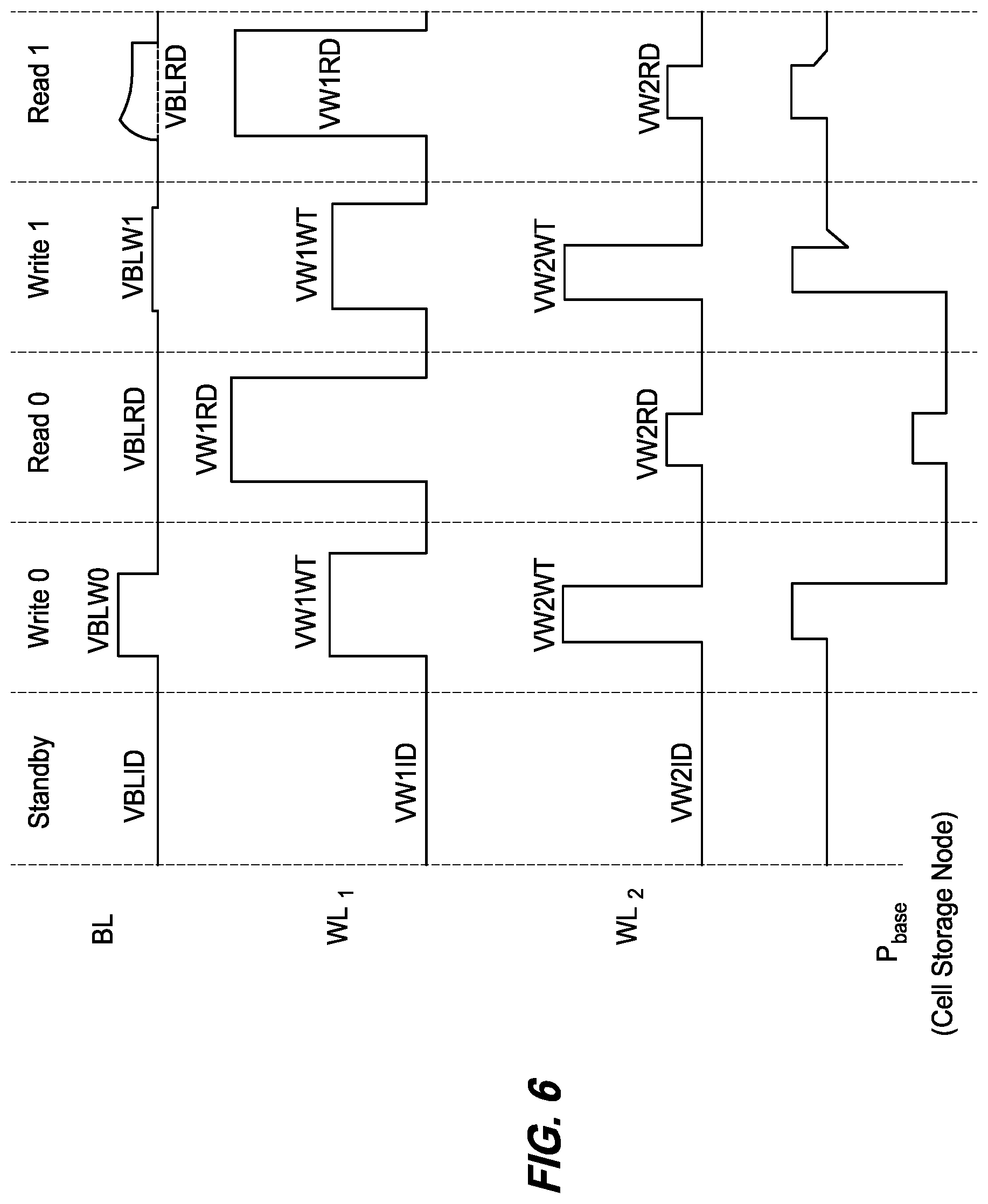
The memory cells of FIGS. 1-4 may be utilized in memory arrays. FIG. 5 diagrammatically illustrates a memory array 50 comprising a plurality of memory cells 10 of the type described above with reference to FIG. 1. Each memory cell is schematically illustrated as a gated BJT, with the gate 26 illustrated to be capacitively coupled to the base 12 (the capacitive coupling is through the dielectric 30, which is not shown in FIG. 5). The illustrated BJTs of FIG. 5 have the region 14 as the emitter region and the region 16 as the collector region, but such orientation may be reversed in other embodiments.
The memory array 50 comprises a series of bitlines, a first series of wordlines (the series identified as WL.sub.1), and a second series of wordlines (the series identified as WL.sub.2). In some embodiments, the node 20 of FIG. 1 may correspond to a bitline (BL), the node 18 of FIG. 1 may correspond to a wordline of the first series (WL.sub.1), and the gate 26 of FIG. 1 may be along a wordline of the second series (WL.sub.2). In such embodiments, the emitter/collector regions 16 of memory cells 10 may be considered to be first emitter/collector regions which are directly coupled with bitlines, and the emitter/collector regions 14 of the memory cells may be considered to be second emitter/collector regions which are electrically coupled with the first series of wordlines. Each memory cell of array 50 may be uniquely addressed through combinations containing one of the bitlines together with one of the wordlines WL.sub.2 and/or one of the wordlines WL.sub.1. The wordlines may be alternatively referred to as access lines in some embodiments, and the bitlines may be alternatively referred to as sense lines in some embodiments.
FIG. 6 diagrammatically illustrates various operations that may be utilized for programming individual memory cells of the array 50 into a "0" data state (i.e., "write 0" operations), programming the individual memory cells into a "1" data state (i.e., "write 1" operations), and for reading the memory cells to ascertain the data states of the individual memory cells. FIG. 6 also diagrammatically illustrates voltage of the P.sub.base (i.e., the base 12 of FIG. 1) during the various operations. Example voltage levels for the various states indicated in FIG. 6 may include (assuming a bandgap of 2.3 eV): VBLID=0 Volt (V) VBLW0=2V VBLRD=0V (D0, 0V; D1, 1V) VBLW1=0V VW1ID=0V VW1WT=3V VW1RD=5V VW2ID=-3V VW2WT=2V VW2RD=-2V
The terms "D0" and "D1" indicate voltages read for the "0" data state and the "1" data state, respectively, of the memory cell. The example operations of FIG. 6 may advantageously achieve a high p-base programming margin (greater than or equal to about 1 V) between the D0 and D1 memory states of the memory cell, which may provide a sufficient charge to enable long retention by the memory cell, and to provide a margin against variation and disturb modes. Also, the various voltages utilized for the reading and writing operations may be kept at relatively low levels (less than or equal to about 5 V) which may enable operation of the memory cell with modest power drain.
Another set of example voltage levels for the various states indicated in FIG. 6 may include (assuming a bandgap of 2.3 eV): VBLID=0V VBLW0=3V VBLRD=0V (D0, 0V; D1, 1V) VBLW1=0V VW1ID=0V VW1WT=5V VW1RD=5V VW2ID=-3V VW2WT=2V VW2RD=-2V
It is noted that the "write 0" operation has a lower voltage differential between WL.sub.1 and the bitline than does the "write 1" operation. The lower voltage differential between the bitline and WL.sub.1 allows charge to drain from the P.sub.base, while the higher voltage differential between the bitline and WL.sub.1 results in charge being trapped on the P.sub.base. Various mechanisms may account for such relationship. For instance, high-voltage differentials between the bitline and WL.sub.1 during capacitive coupling of the base with gate 26 can lead to impact ionization, a Kirk effect, a Webster effect and/or other mechanisms which limit charge transfer through the BJT, and thus can lead to charge being trapped on the floating base of the BJT. In contrast, low-voltage differentials between the bitline and WL.sub.1_during the capacitive coupling of the gate with the base may permit a steady flow of charge through the BJT, and thus may permit charge to be drained from the floating base.
A possible explanation for the reason that the lower voltage differential between the bitline and WL.sub.1 allows charge to drain from the P.sub.base, while the higher voltage differential between the bitline and WL.sub.1 results in charge being trapped on the P.sub.base is as follows. When the voltage differential is high, there is impact ionization in the collector-base region. This supplies a base current (I.sub.b) to the npn bipolar transistor. A collector current (I.sub.c) results, which is related to the base current through Equation II. I.sub.c=.beta.*I.sub.b Equation II
In Equation II, .beta. is the npn current gain.
The impact ionization current is equal to .alpha..sub.n*I.sub.c, where an is the impact ionization efficiency; and is a function of electric field divided by voltage. This leads to the relationship of Equation III. I.sub.b=.alpha..sub.n*I.sub.c Equation III
If (.alpha..sub.n*.beta.)>1, the cell latches. Once the cell latches, the gate (26 of FIG. 5) losses control of the P.sub.base and cannot couple to it. Hence, even if the gate voltage is brought down, the P.sub.base voltage stays high. In contrast, with a low voltage differential the cell does not latch, the gate has good coupling to the P.sub.base, and pulling the gate voltage down will also pull the P.sub.base voltage down.
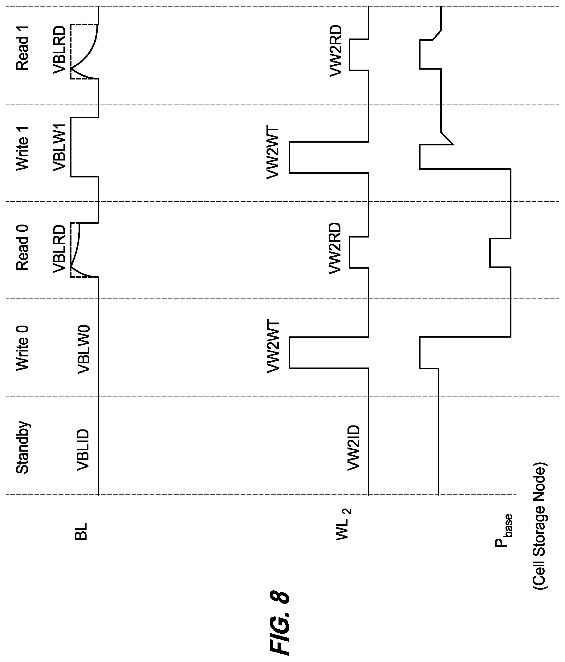
FIG. 7 diagrammatically illustrates an example embodiment memory array 50a comprising a plurality of memory cells 10 of the type described above with reference to FIG. 1. The memory array of FIG. 7 is similar to that of FIG. 5, except that the first series of wordlines (WL.sub.1 of FIG. 5) has been replaced with nodes 51. The nodes 51 are at a common voltage as one another, and in some embodiments may be electrically coupled with one another and with a common terminal (for instance, they may all be connected to a grounded plate).
In some embodiments, the node 20 of FIG. 1 may correspond to the bitline (BL) of FIG. 7, the node 18 of FIG. 1 may correspond to a node 51, and the gate 26 of FIG. 1 may be along a wordline of the series (WL.sub.2). In such embodiments, the emitter/collector regions 16 of memory cells 10 may be considered to be first emitter/collector regions which are directly coupled with bitlines, and the emitter/collector regions 14 of the memory cells may be considered to be second emitter/collector regions which are electrically coupled with one another and with a common terminal. Each memory cell of array 50a may be uniquely addressed through combinations containing one of the bitlines together with one of the wordlines WL.sub.2.
FIG. 8 diagrammatically illustrates various operations that may be utilized for programming individual memory cells of the array 50a into a "0" data state (i.e., "write 0" operations), programming the individual memory cells into a "1" data state (i.e., "write 1" operations), and for reading the memory cells to ascertain the data states of the individual memory cells. FIG. 8 also diagrammatically illustrates voltage of the P.sub.base (i.e., the base 12 of FIG. 1) during the various operations. Example voltage levels for the various states indicated in FIG. 8 may include (assuming a bandgap of 2.3 eV, and assuming a common voltage on nodes 51 of 0V): VBLID=2V VBLW0=2V VBLRD=5V (D0, 5V; D1, 4V) VBLW1=4V VW2ID=-3V VW2WT=2V VW2RD=-1.4V
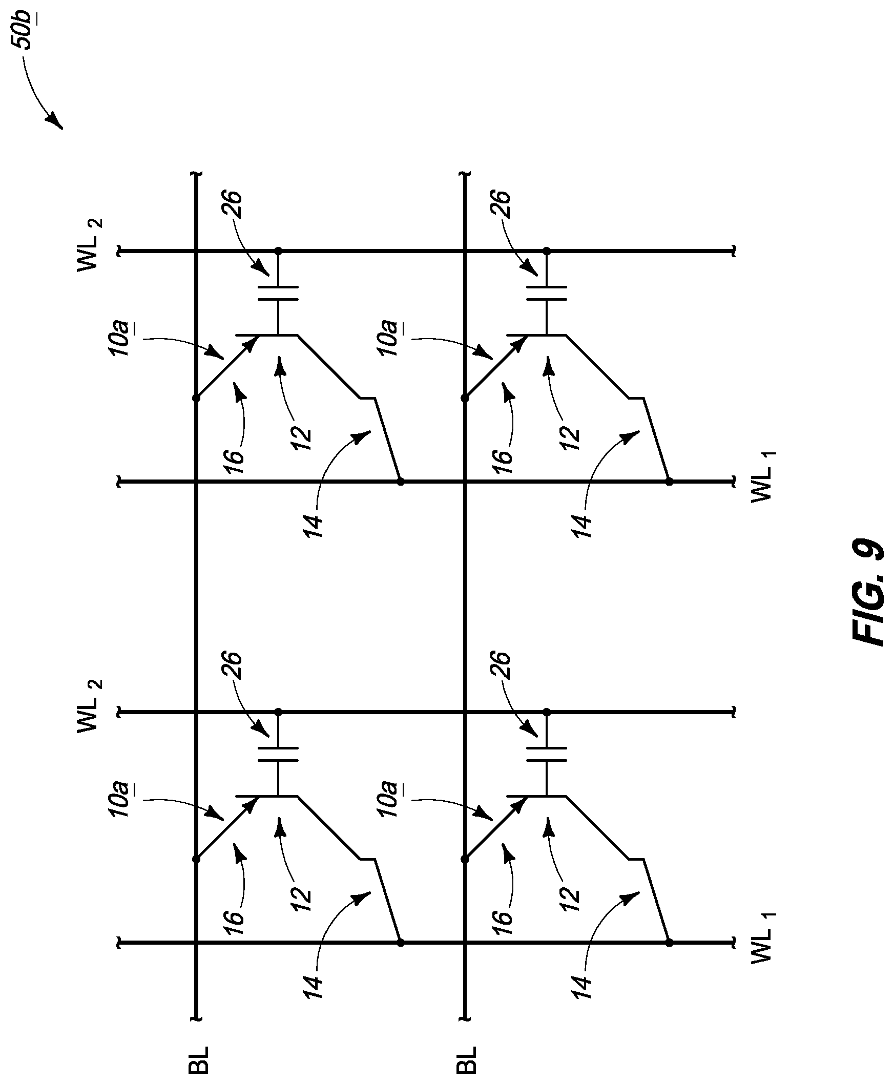
FIG. 9 diagrammatically illustrates another example embodiment memory array 50b. The memory array of FIG. 9 comprises a plurality of memory cells 10a of the type described above with reference to FIG. 2. The memory array of FIG. 9, like that of FIG. 5, comprises a series of bitlines, a first series of wordlines (the series identified as WL.sub.1), and a second series of wordlines (the series identified as WL.sub.2). In some embodiments, the node 20 of FIG. 2 may correspond to a bitline (BL), the node 18 of FIG. 2 may correspond to a wordline of the first series (WL.sub.1), and the gate 26 of FIG. 2 may be along a wordline of the second series (WL.sub.2). In such embodiments, the emitter/collector regions 16 of memory cells 10a may be considered to be first emitter/collector regions which are directly coupled with bitlines, and the emitter/collector regions 14 of the memory cells may be considered to be second emitter/collector region which are electrically coupled with the first series of wordlines. Each memory cell of array 50b may be uniquely addressed through combinations containing one of the bitlines together with one of the wordlines WL.sub.2 and/or one of the wordlines WL.sub.1.
FIG. 10 diagrammatically illustrates various operations that may be utilized for programming individual memory cells of the array 50b into a "0" data state (i.e., "write 0" operations), programming the individual memory cells into a "1" data state (i.e., "write 1" operations), and for reading the memory cells to ascertain the data states of the individual memory cells. FIG. 10 also diagrammatically illustrates voltage of the N.sub.base (i.e., the base 12 of FIG. 2) during the various operations. Example voltage levels for the various states indicated in FIG. 10 may include (assuming a bandgap of 2.3 eV): VBLID=5V VBLW0=4V VBLRD=5V (D0, 5V; D1, 4V) VBLW1=5V VW1ID=5V VW1WT=1V VW1RD=0V VW2ID=5V VW2WT=0V VW2RD=4V
Another set of example voltage levels for the various states indicated in FIG. 10 may include (assuming a bandgap of 2.3 eV): VBLID=5V VBLW0=3V VBLRD=5V (D0, 5V; D1, 4V) VBLW1=5V VW1ID=5V VW1WT=0V VW1RD=0V VW2ID=5V VW2WT=0V VW2RD=4V
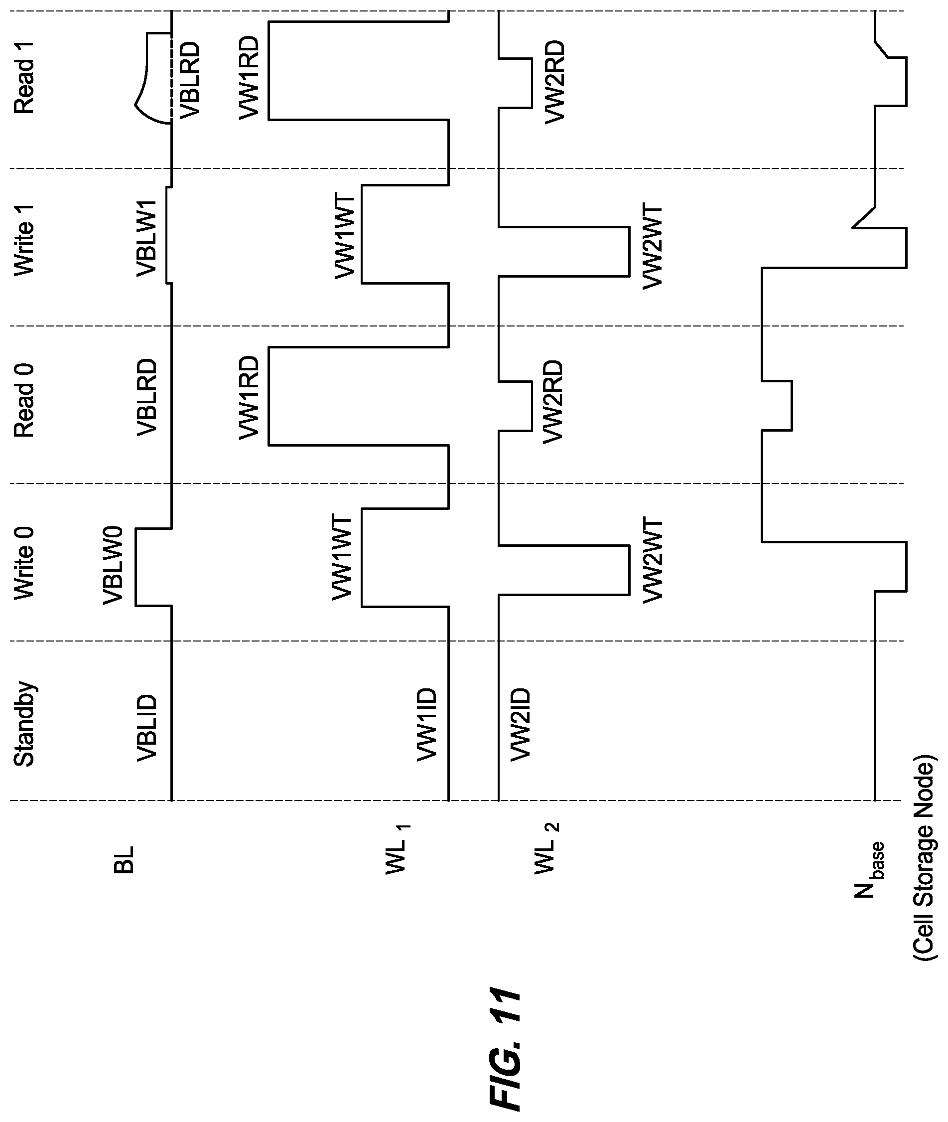
FIG. 11 diagrammatically illustrates another set of operations that may be utilized for programming individual memory cells of the array 50b of FIG. 9 into a "0" data state (i.e., "write 0" operations), programming the individual memory cells into a "1" data state (i.e., "write 1" operations), and for reading the memory cells to ascertain the data states of the individual memory cells. FIG. 11 also diagrammatically illustrates voltage of the N.sub.base (i.e., the base 12 of FIG. 2) during the various operations. Example voltage levels for the various states indicated in FIG. 11 may include (assuming a bandgap of 2.3 eV): VBLID=0V VBLW0=2V VBLRD=0V (D0, 0V; D1, 1V) VBLW1=0V VW1ID=0V VW1WT=4V VW1RD=5V VW2ID=5V VW2WT=0V VW2RD=4V
Another set of example voltage levels for the various states indicated in FIG. 11 may include (assuming a bandgap of 2.3 eV): VBLID=0V VBLW0=3V VBLRD=0V (D0, 0V; D1, 1V) VBLW1=0V VW1ID=0V VW1WT=5V VW1RD=5V VW2ID=5V VW2WT=0V VW2RD=4V
FIG. 12 diagrammatically illustrates an example embodiment memory array 50c comprising a plurality of memory cells 10a of the type described above with reference to FIG. 2. The memory array of FIG. 12 is similar to that of FIG. 9, except that the first series of wordlines (WL.sub.1 of FIG. 9) have been replaced with nodes 53. The nodes 53 are at a common voltage as one another, and in some embodiments may be electrically coupled with one another and with a common terminal (for instance, they may all be connected to an electrically conductive plate).
In some embodiments, the node 20 of FIG. 2 may correspond to the bitline (BL) of FIG. 12, the node 18 of FIG. 2 may correspond to a node 53, and the gate 26 of FIG. 2 may be along a wordline of the series (WL.sub.2). In such embodiments, the emitter/collector regions 16 of memory cells 10a may be considered to be first emitter/collector regions which are directly coupled with bitlines, and the emitter/collector regions 14 of the memory cells may be considered to be second emitter/collector regions which are electrically coupled with one another and with a common terminal. Each memory cell of array 50c may be uniquely addressed through combinations containing one of the bitlines together with one of the wordlines WL.sub.2.
FIG. 13 diagrammatically illustrates various operations that may be utilized for programming individual memory cells of the array 50c into a "0" data state (i.e., "write 0" operations), programming the individual memory cells into a "1" data state (i.e., "write 1" operations), and for reading the memory cells to ascertain the data states of the individual memory cells. FIG. 13 also diagrammatically illustrates voltage of the N.sub.base (i.e., the base 12 of FIG. 2) during the various operations. Example voltage levels for the various states indicated in FIG. 13 may include (assuming a bandgap of 2.3 eV, and assuming a common voltage on nodes 53 of 5V): VBLID=3V VBLW0=3V VBLRD=0V (D0, 0V; D1, 1V) VBLW1=0V VW2ID=5V VW2WT=0V VW2RD=3.4V
FIG. 14 diagrammatically illustrates another set of operations that may be utilized for programming individual memory cells of the array 50c of FIG. 12 into a "0" data state (i.e., "write 0" operations), programming the individual memory cells into a "1" data state (i.e., "write 1" operations), and for reading the memory cells to ascertain the data states of the individual memory cells. FIG. 14 also diagrammatically illustrates voltage of the N.sub.base (i.e., the base 12 of FIG. 2) during the various operations. Example voltage levels for the various states indicated in FIG. 14 may include (assuming a bandgap of 2.3 eV, and assuming a common voltage on nodes 53 of 0V): VBLID=2V VBLW0=2V VBLRD=5V (D0, 5V; D1, 4V) VBLW1=4V VW2ID=5V VW2WT=0V VW2RD=3.4V
The memory cells of FIGS. 1-4 may be readily incorporated into semiconductor constructions. FIGS. 15 and 16 illustrate example semiconductor constructions comprising the memory cell 10 of FIG. 1, and the memory cell 10a of FIG. 2, respectively.
Referring to FIG. 15, a semiconductor construction 60 comprises memory cell 10 supported over a semiconductor substrate 62. The substrate 62 may comprise, consist essentially of, or consist of monocrystalline silicon in some embodiments, and is shown to be p-type background doped. The terms "semiconductive substrate," "semiconductor construction" and "semiconductor substrate" mean any construction comprising semiconductive material, including, but not limited to, bulk semiconductive materials such as a semiconductive wafer (either alone or in assemblies comprising other materials), and semiconductive material layers (either alone or in assemblies comprising other materials). The term "substrate" refers to any supporting structure, including, but not limited to, the semiconductive substrates described above. Although substrate 62 is shown to be homogenous, the substrate may comprise numerous materials in some embodiments. For instance, substrate 62 may correspond to a semiconductor substrate containing one or more materials associated with integrated circuit fabrication. Example materials that may be associated with integrated circuit fabrication are various of refractory metal materials, barrier materials, diffusion materials, insulator materials, etc.
The memory cell 10 is part of a substantially vertical pillar 64. Such pillar includes an n-type doped segment 66 directly over the semiconductor material of substrate 62 (the segment 66 is shown doped to an n+ dopant level). In some embodiments, segment 66 may comprise monocrystalline silicon patterned from substrate 62, and/or may comprise semiconductor material deposited over substrate 62. The segment 66 is shown electrically coupled with an electrically conductive material 68 that interconnects with node 18. The conductive material 68 may be any suitable material; including, for example, any of various metals, metal-containing compositions, and/or conductive-doped semiconductor materials. The conductive material 68 may be a separate material from the conductively-doped material of segment 66 (as shown), or may be an extension of the conductively-doped material 66. In some embodiments, segment 66 may be omitted and emitter/collector region may directly contact a conductive node 18 comprising, consisting essentially of, or consisting of any of various metals and/or metal-containing compositions.
The pillar 64 is referred to as being "substantially vertical" to indicate that it extends substantially orthogonally to a primary upper surface of the substrate. Specifically, the term "vertical" is used herein to define a relative orientation of an element or structure with respect to a major plane or surface of a wafer or substrate. A structure may be referred to as being "substantially vertical" to indicate that the structure is vertical to within reasonable tolerances of fabrication and measurement.
The pillar 64 also includes an n-type doped segment 70 directly over the emitter/collector region 16. The segment 70 may comprise silicon and/or any other suitable semiconductor material. The segment 70 is shown electrically coupled with an electrically conductive material 72 that interconnects with node 20. The conductive material 72 may be any suitable material; including, for example, any of various metals, metal-containing compositions, and/or conductive-doped semiconductor materials. The conductive material 72 may be a separate material from the conductively-doped material of segment 70 (as shown), or may be an extension of the conductively-doped material 70. In some embodiments, segment 70 may be omitted and emitter/collector region 16 may directly contact a conductive node 20 comprising, consisting essentially of, or consisting of any of various metals and/or metal-containing compositions.
Referring to FIG. 16, a semiconductor construction 60a comprises memory cell 10a supported over a semiconductor substrate 62a. The substrate 62a may comprise any of the compositions discussed above with reference to the substrate 62 of FIG. 15.
The memory cell 10a is part of a substantially vertical pillar 64a. Such pillar includes a p-type doped segment 66a directly over the semiconductor material of substrate 62a. The segment 66a is shown electrically coupled with an electrically conductive material 68a that interconnects with node 18. The conductive material 68a may be any of the materials discussed above with reference to the material 68 of FIG. 15. The conductive material 68a may be a separate material from the conductively-doped material of segment 66a (as shown), or may be an extension of the conductively-doped material 66a. In some embodiments, segment 66a may be omitted and emitter/collector region may directly contact a conductive node 18 comprising, consisting essentially of, or consisting of any of various metals and/or metal-containing compositions.
The pillar 64a also includes a p-type doped segment 70a directly over the emitter/collector region 16. The segment 70a may comprise silicon and/or any other suitable semiconductor material. The segment 70a is shown electrically coupled with an electrically conductive material 72a that interconnects with node 20. The conductive material 72a may comprise any of the materials discussed above with reference to the material 72 of FIG. 15. The conductive material 72a may be a separate material from the conductively-doped material of segment 70a (as shown), or may be an extension of the conductively-doped material 70a. In some embodiments, segment 70a may be omitted and emitter/collector region 16 may directly contact a conductive node 20 comprising, consisting essentially of, or consisting of any of various metals and/or metal-containing compositions.
In some embodiments, the memory cells having wide-bandgap material may be formed along one or more levels (or tiers) of an integrated circuit chip, and may be formed over one or more levels of logic or other circuitry fabricated by conventional methods (for instance, such other circuitry may comprise metal-oxide-semiconductor field-effect transistors (MOSFET). Additionally, or alternatively, one or more levels of conventional circuitry may be fabricated over the memory cells containing the wide-bandgap material.
The various memory cells and memory arrays of FIGS. 1-16 may be formed utilizing any suitable processing. For instance, FIGS. 17 and 18 illustrate an example process for fabricating a memory array 50a of the type shown in FIG. 7 comprising memory cells 10 of the type shown in FIG. 1.
Referring to FIG. 17, a semiconductor construction 80 comprises a substrate 82 having an n-type doped region 83 over a p-type doped region 81. The substrate 82 may be a semiconductor substrate analogous to the substrate 62 discussed above with reference to FIG. 15. Accordingly, the regions 81 and 83 may be conductively-doped regions of a monocrystalline silicon wafer, and/or may be conductively-doped regions formed along a tier of a partially-fabricated integrated circuit.
Conductively-doped regions 12, 14 and 16 of a memory cell stack 84 are formed over substrate 82. In some embodiments, the entire stack 84 may comprise, consist essentially of, or consist of doped wide-bandgap material (such as, for example, 3C--SiC). If doped region 83 comprises monocrystalline silicon and the wide-bandgap material comprises silicon carbide, the wide-bandgap material may be epitaxially grown over the monocrystalline silicon.
A difficulty encountered in incorporating wide-bandgap materials (such as, for example, silicon carbide) into integrated circuit fabrication sequences is that dopant activation within the wide-bandgap materials may utilize a thermal budget which is too high for many of the components conventionally utilized in integrated circuitry. A method of reducing the thermal budget for dopant activation is to in situ dope the wide-bandgap material during epitaxial growth of such material.
A patterned mask 97 is formed over memory cell stack 84, with such patterned mask defining a pattern corresponding to a plurality of openings 99 that extend through the mask. The patterned mask may comprise any suitable composition and may be formed with any suitable processing. For instance, the mask may comprise photolithographically-patterned photoresist. As another example, the mask may comprise one or more structures formed utilizing pitch multiplication methodologies.
Referring to FIG. 18, a pattern is transferred from mask 97 (FIG. 17) into stack 84 with one or more suitable etches, and then the mask is removed. The memory cell stack 84 is thus patterned into substantially vertical BJT pillars 88. Subsequently, dielectric material 30 is formed along sidewalls of the pillars.
Electrically-conductive interconnects 90 are formed between the pillars and in electrical connection with doped region 83. The interconnects 90 may be electrically coupled with one another through doped region 83 and/or through other interconnections, and may all be electrically connected to a common terminal so that they are all tied to the common voltage 51 (as shown).
The dielectric material 30 may be formed by initially providing surface passivation along outer exposed surfaces of pillars 88. Such surface passivation may comprise providing a layer containing silicon, oxygen and nitrogen along the outer surfaces. Such layer may be formed by nitridation/oxidation of exposed outer surfaces of silicon carbide in some embodiments, and/or by deposition of passivation material along the exposed outer surfaces. The dielectric material 30 may consist of the passivation layer in some embodiments. In other embodiments, additional dielectric materials may be formed along the passivation layer to form a dielectric material 30 comprising the passivation layer in combination with other dielectric materials. Such other dielectric materials may comprise, for example, one or both of silicon dioxide and silicon nitride.
In some embodiments, material 90 may comprise metal or other thermally-sensitive material, and an advantage of forming conductive material 90 after the doping of wide-bandgap material is that such can avoid exposure of the thermally-sensitive material to the thermal budget utilized for the doping of the wide-bandgap material.
Electrically insulative material 92 is formed over conductive material 90 and between the pillars 88, and then the conductive material 27 is formed and patterned over insulative material 92 to form the gates 26. Subsequently, another insulative material 94 is formed over gates 26 and insulative material 92. The electrically insulative materials 92 and 94 may comprise any suitable compositions or combinations of compositions, including for example, one or more of silicon dioxide, silicon nitride, and any of various doped oxide glasses (for instance, borophosphosilicate glass, phosphosilicate glass, fluorosilicate glass, etc.). The electrically insulative materials 92 and 94 may be the same composition as one another in some embodiments, and may differ in composition from one another in other embodiments.
A bitline 100 is formed across the pillars 88, and in direct electrical contact with the upper doped regions 16 within such pillars. The bitline 100 may be considered to be an example of a node 20 (FIG. 1) that may be formed in direct electrical connection with the upper emitter/collector regions 16 of the illustrated example embodiment memory cells. Bitline 100 may comprise any suitable electrically conductive material, and may, for example, comprise, consist essentially of, or consist of one or more of various metals, metal-containing compositions and conductively-doped semiconductor materials. Although the bitline is shown formed directly against the emitter/collector region 16, in other embodiments there may be one or more electrically-conductive materials between the bitline and the emitter/collector region (such as, for example, an electrically conductive material analogous to the conductively-doped semiconductor material 70 of FIG. 15).
The construction 80 has a dimension from one side of a pillar to a same side of an adjacent pillar of 2F, and thus the individual memory cells may have footprints of about 4F.sup.2.
Although FIGS. 17 and 18 pertain to formation of memory cells 10 of the type shown in FIG. 1 in a memory array of the type shown in FIG. 7, persons of ordinary skill will recognize that similar processing may be utilized to form any of the other memory cells described in this disclosure in any of the memory arrays described in this disclosure.
The memory cells and memory arrays discussed above may be incorporated into integrated circuit chips or packages, and such may utilized in electronic devices and/or systems. The electronic systems may be used in, for example, memory modules, device drivers, power modules, communication modems, processor modules, and application-specific modules, and may include multilayer, multichip modules. The electronic systems may be any of a broad range of systems, such as, for example, clocks, televisions, cell phones, personal computers, automobiles, industrial control systems, aircraft, etc.
The particular orientation of the various embodiments in the drawings is for illustrative purposes only, and the embodiments may be rotated relative to the shown orientations in some applications. The description provided herein, and the claims that follow, pertain to any structures that have the described relationships between various features, regardless of whether the structures are in the particular orientation of the drawings, or are rotated relative to such orientation.
The cross-sectional views of the accompanying illustrations only show features within the planes of the cross-sections, and do not show materials behind the planes of the cross-sections in order to simplify the drawings.
When a structure is referred to above as being "on" or "against" another structure, it can be directly on the other structure or intervening structures may also be present. In contrast, when a structure is referred to as being "directly on" or "directly against" another structure, there are no intervening structures present. When a structure is referred to as being "connected" or "coupled" to another structure, it can be directly connected or coupled to the other structure, or intervening structures may be present. In contrast, when a structure is referred to as being "directly connected" or "directly coupled" to another structure, there are no intervening structures present.
In compliance with the statute, the subject matter disclosed herein has been described in language more or less specific as to structural and methodical features. It is to be understood, however, that the claims are not limited to the specific features shown and described, since the means herein disclosed comprise example embodiments. The claims are thus to be afforded full scope as literally worded, and to be appropriately interpreted in accordance with the doctrine of equivalents.
* * * * *
References
D00000
D00001
D00002
D00003
D00004
D00005
D00006
D00007
D00008
D00009
D00010
D00011
D00012

D00013

D00014
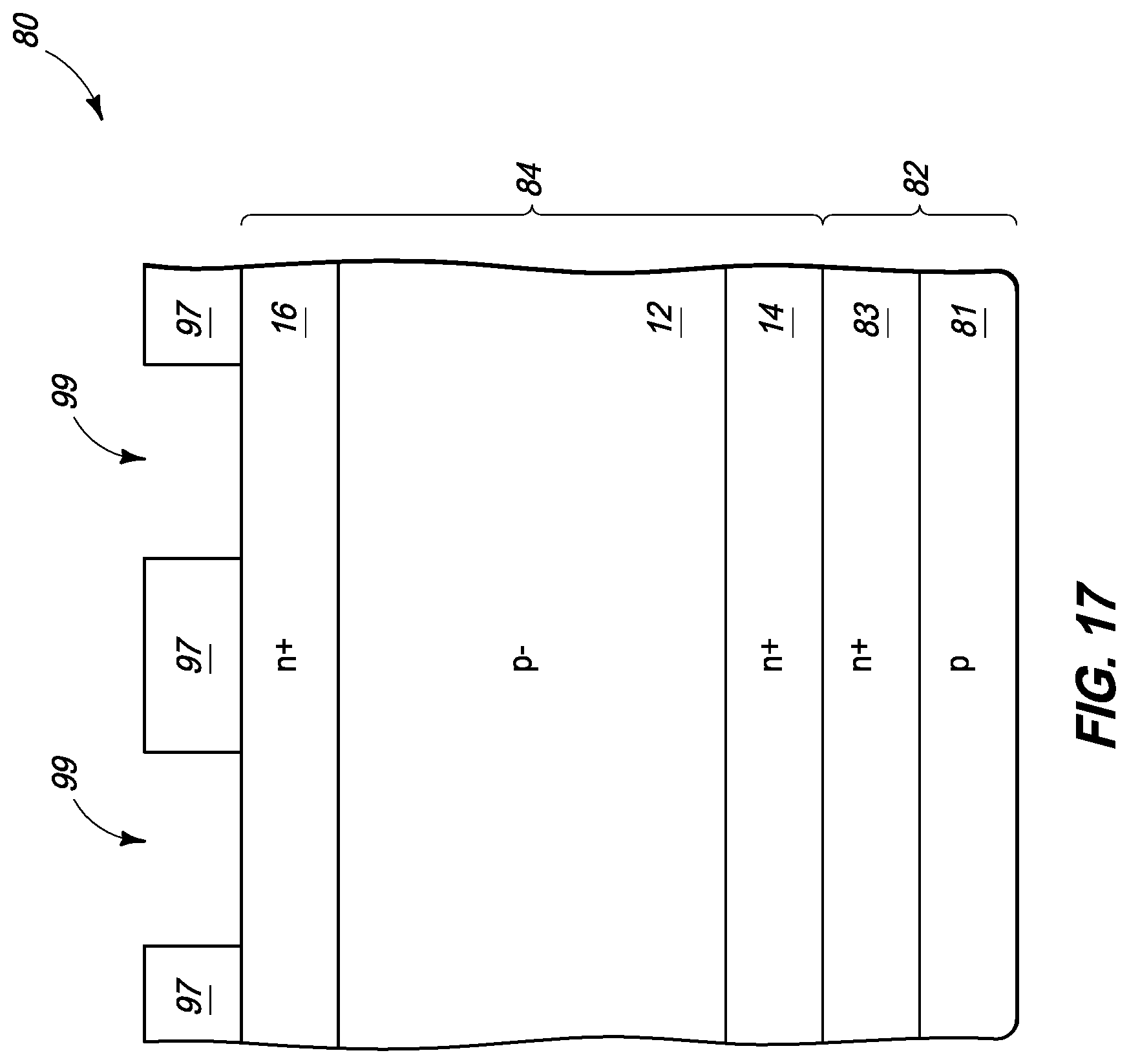
D00015
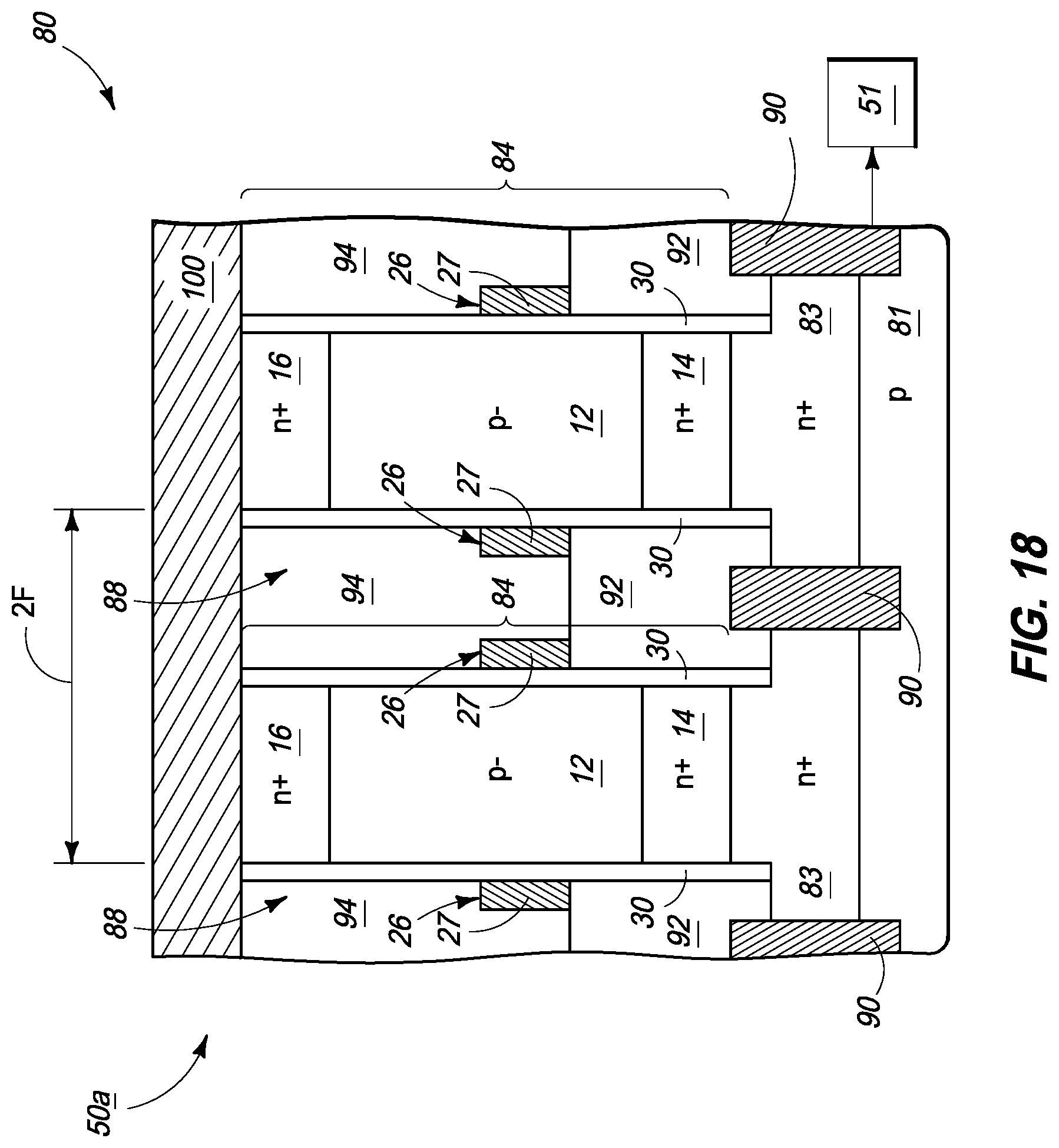
M00001

XML
uspto.report is an independent third-party trademark research tool that is not affiliated, endorsed, or sponsored by the United States Patent and Trademark Office (USPTO) or any other governmental organization. The information provided by uspto.report is based on publicly available data at the time of writing and is intended for informational purposes only.
While we strive to provide accurate and up-to-date information, we do not guarantee the accuracy, completeness, reliability, or suitability of the information displayed on this site. The use of this site is at your own risk. Any reliance you place on such information is therefore strictly at your own risk.
All official trademark data, including owner information, should be verified by visiting the official USPTO website at www.uspto.gov. This site is not intended to replace professional legal advice and should not be used as a substitute for consulting with a legal professional who is knowledgeable about trademark law.