Semiconductor package with reduced parasitic coupling effects and process for making the same
Costa , et al. January 5, 2
U.S. patent number 10,886,148 [Application Number 15/975,230] was granted by the patent office on 2021-01-05 for semiconductor package with reduced parasitic coupling effects and process for making the same. This patent grant is currently assigned to Qorvo US, Inc.. The grantee listed for this patent is Qorvo US, Inc.. Invention is credited to Julio C. Costa, Dirk Robert Walter Leipold, George Maxim, Baker Scott.


View All Diagrams
| United States Patent | 10,886,148 |
| Costa , et al. | January 5, 2021 |
Semiconductor package with reduced parasitic coupling effects and process for making the same
Abstract
The present disclosure relates to a semiconductor package with reduced parasitic coupling effects, and a process for making the same. The disclosed semiconductor package includes a thinned flip-chip die and a first mold compound component with a dielectric constant no more than 7. The thinned flip-chip die includes a back-end-of-line (BEOL) layer with an upper surface that includes a first surface portion and a second surface portion surrounding the first surface portion, a device layer over the upper surface of the BEOL layer, and a buried oxide (BOX) layer over the device layer. The BEOL layer includes a first passive device and a second passive device, which are underlying the first surface portion and not underlying the second surface portion. Herein, the first mold compound component extends through the BOX layer and the device layer to the first surface portion.
| Inventors: | Costa; Julio C. (Oak Ridge, NC), Maxim; George (Saratoga, CA), Leipold; Dirk Robert Walter (San Jose, CA), Scott; Baker (San Jose, CA) | ||||||||||
|---|---|---|---|---|---|---|---|---|---|---|---|
| Applicant: |
|
||||||||||
| Assignee: | Qorvo US, Inc. (Greensboro,
NC) |
||||||||||
| Family ID: | 1000005284414 | ||||||||||
| Appl. No.: | 15/975,230 | ||||||||||
| Filed: | May 9, 2018 |
Prior Publication Data
| Document Identifier | Publication Date | |
|---|---|---|
| US 20180261470 A1 | Sep 13, 2018 | |
Related U.S. Patent Documents
| Application Number | Filing Date | Patent Number | Issue Date | ||
|---|---|---|---|---|---|
| 15498040 | Apr 26, 2017 | 10109502 | |||
| 62393201 | Sep 12, 2016 | ||||
| Current U.S. Class: | 1/1 |
| Current CPC Class: | H01L 29/78 (20130101); H01L 21/561 (20130101); H01L 28/40 (20130101); H01L 23/5223 (20130101); H01L 23/295 (20130101); H01L 23/3135 (20130101); H01L 29/0649 (20130101); H01L 23/3114 (20130101); H01L 2924/1306 (20130101); H01L 2224/32225 (20130101); H01L 2924/18161 (20130101); H01L 2224/32245 (20130101); H01L 2224/73204 (20130101); H01L 2224/16245 (20130101); H01L 2224/11002 (20130101); H01L 2224/16227 (20130101); H01L 23/5222 (20130101); H01L 2224/92125 (20130101); H01L 2224/73204 (20130101); H01L 2224/16245 (20130101); H01L 2224/32245 (20130101); H01L 2924/00 (20130101) |
| Current International Class: | H01L 21/56 (20060101); H01L 49/02 (20060101); H01L 23/31 (20060101); H01L 29/06 (20060101); H01L 29/78 (20060101); H01L 23/29 (20060101); H01L 23/522 (20060101) |
References Cited [Referenced By]
U.S. Patent Documents
| 4093562 | June 1978 | Kishimoto |
| 4366202 | December 1982 | Borovsky |
| 5013681 | May 1991 | Godbey et al. |
| 5061663 | October 1991 | Bolt et al. |
| 5069626 | December 1991 | Patterson et al. |
| 5362972 | November 1994 | Yazawa et al. |
| 5391257 | February 1995 | Sullivan et al. |
| 5459368 | October 1995 | Onishi et al. |
| 5646432 | July 1997 | Iwaki et al. |
| 5648013 | July 1997 | Uchida et al. |
| 5699027 | December 1997 | Tsuji et al. |
| 5709960 | January 1998 | Mays et al. |
| 5729075 | March 1998 | Strain |
| 5831369 | November 1998 | Furbacher et al. |
| 5920142 | July 1999 | Onishi et al. |
| 6072557 | June 2000 | Kishimoto |
| 6084284 | July 2000 | Adamic, Jr. |
| 6154366 | November 2000 | Ma et al. |
| 6154372 | November 2000 | Kalivas et al. |
| 6235554 | May 2001 | Akram et al. |
| 6236061 | May 2001 | Walpita |
| 6268654 | July 2001 | Glenn et al. |
| 6271469 | August 2001 | Ma et al. |
| 6377112 | April 2002 | Rozsypal |
| 6423570 | July 2002 | Ma et al. |
| 6426559 | July 2002 | Bryan et al. |
| 6441498 | August 2002 | Song |
| 6446316 | September 2002 | Furbacher et al. |
| 6578458 | June 2003 | Akram et al. |
| 6649012 | November 2003 | Masayuki et al. |
| 6713859 | March 2004 | Ma |
| 6841413 | January 2005 | Liu et al. |
| 6864156 | March 2005 | Conn |
| 6902950 | June 2005 | Ma et al. |
| 6943429 | September 2005 | Glenn et al. |
| 6964889 | November 2005 | Ma et al. |
| 6992400 | January 2006 | Tikka et al. |
| 7042072 | May 2006 | Kim et al. |
| 7049692 | May 2006 | Nishimura et al. |
| 7109635 | September 2006 | McClure et al. |
| 7183172 | February 2007 | Lee et al. |
| 7238560 | July 2007 | Sheppard et al. |
| 7279750 | October 2007 | Jobetto |
| 7288435 | October 2007 | Aigner et al. |
| 7307003 | December 2007 | Reif et al. |
| 7393770 | July 2008 | Wood et al. |
| 7402901 | July 2008 | Hatano et al. |
| 7427824 | September 2008 | Iwamoto et al. |
| 7489032 | February 2009 | Jobetto |
| 7596849 | October 2009 | Carpenter et al. |
| 7619347 | November 2009 | Bhattacharjee |
| 7635636 | December 2009 | McClure et al. |
| 7714535 | May 2010 | Yamazaki et al. |
| 7749882 | July 2010 | Kweon et al. |
| 7790543 | September 2010 | Abadeer et al. |
| 7843072 | November 2010 | Park et al. |
| 7855101 | December 2010 | Furman et al. |
| 7868419 | January 2011 | Kerr et al. |
| 7910405 | March 2011 | Okada et al. |
| 7960218 | June 2011 | Ma et al. |
| 8004089 | August 2011 | Jobetto |
| 8183151 | May 2012 | Lake |
| 8420447 | April 2013 | Tay et al. |
| 8503186 | August 2013 | Lin et al. |
| 8643148 | February 2014 | Lin et al. |
| 8658475 | February 2014 | Kerr |
| 8664044 | March 2014 | Jin et al. |
| 8772853 | July 2014 | Hong et al. |
| 8791532 | July 2014 | Graf et al. |
| 8802495 | August 2014 | Kim et al. |
| 8803242 | August 2014 | Marino et al. |
| 8816407 | August 2014 | Kim et al. |
| 8835978 | September 2014 | Mauder et al. |
| 8906755 | December 2014 | Hekmatshoartabari et al. |
| 8921990 | December 2014 | Park et al. |
| 8927968 | January 2015 | Cohen et al. |
| 8941248 | January 2015 | Lin et al. |
| 8963321 | February 2015 | Lenniger et al. |
| 8983399 | March 2015 | Kawamura et al. |
| 9165793 | October 2015 | Wang et al. |
| 9214337 | December 2015 | Carroll et al. |
| 9349700 | May 2016 | Hsieh et al. |
| 9368429 | June 2016 | Ma et al. |
| 9461001 | October 2016 | Tsai et al. |
| 9520428 | December 2016 | Fujimori |
| 9530709 | December 2016 | Leipold et al. |
| 9613831 | April 2017 | Morris et al. |
| 9646856 | May 2017 | Meyer et al. |
| 9653428 | May 2017 | Hiner et al. |
| 9786586 | October 2017 | Shih |
| 9812350 | November 2017 | Costa |
| 9824951 | November 2017 | Leipold et al. |
| 9824974 | November 2017 | Gao et al. |
| 9859254 | January 2018 | Yu et al. |
| 9875971 | January 2018 | Bhushan et al. |
| 9941245 | April 2018 | Skeete et al. |
| 10134837 | November 2018 | Fanelli et al. |
| 2001/0004131 | June 2001 | Masayuki et al. |
| 2002/0070443 | June 2002 | Mu et al. |
| 2002/0074641 | June 2002 | Towle et al. |
| 2002/0127769 | September 2002 | Ma et al. |
| 2002/0127780 | September 2002 | Ma et al. |
| 2002/0137263 | September 2002 | Towle et al. |
| 2002/0185675 | December 2002 | Furukawa |
| 2003/0207515 | November 2003 | Tan et al. |
| 2004/0021152 | February 2004 | Nguyen et al. |
| 2004/0164367 | August 2004 | Park |
| 2004/0166642 | August 2004 | Chen et al. |
| 2004/0219765 | November 2004 | Reif et al. |
| 2005/0037595 | February 2005 | Nakahata |
| 2005/0077511 | April 2005 | Fitzergald |
| 2005/0079686 | April 2005 | Aigner et al. |
| 2005/0212419 | September 2005 | Vazan et al. |
| 2006/0057782 | March 2006 | Gardes et al. |
| 2006/0099781 | May 2006 | Beaumont et al. |
| 2006/0105496 | May 2006 | Chen et al. |
| 2006/0108585 | May 2006 | Gan et al. |
| 2006/0228074 | October 2006 | Lipson et al. |
| 2006/0261446 | November 2006 | Wood et al. |
| 2007/0020807 | January 2007 | Geefay et al. |
| 2007/0045738 | March 2007 | Jones et al. |
| 2007/0069393 | March 2007 | Asahi et al. |
| 2007/0075317 | April 2007 | Kato et al. |
| 2007/0121326 | May 2007 | Nall et al. |
| 2007/0158746 | July 2007 | Ohguro |
| 2007/0181992 | August 2007 | Lake |
| 2007/0190747 | August 2007 | Humpston et al. |
| 2007/0194342 | August 2007 | Kinzer |
| 2007/0252481 | November 2007 | Iwamoto et al. |
| 2007/0276092 | November 2007 | Kanae et al. |
| 2008/0050852 | February 2008 | Hwang et al. |
| 2008/0050901 | February 2008 | Kweon et al. |
| 2008/0164528 | July 2008 | Cohen et al. |
| 2008/0265978 | October 2008 | Englekirk |
| 2008/0272497 | November 2008 | Lake |
| 2008/0315372 | December 2008 | Kuan et al. |
| 2009/0008714 | January 2009 | Chae |
| 2009/0010056 | January 2009 | Kuo et al. |
| 2009/0014856 | January 2009 | Knickerbocker |
| 2009/0090979 | April 2009 | Zhu et al. |
| 2009/0179266 | July 2009 | Abadeer et al. |
| 2009/0261460 | October 2009 | Kuan et al. |
| 2009/0302484 | December 2009 | Lee et al. |
| 2010/0003803 | January 2010 | Oka et al. |
| 2010/0012354 | January 2010 | Hedin et al. |
| 2010/0029045 | February 2010 | Ramanathan et al. |
| 2010/0045145 | February 2010 | Tsuda |
| 2010/0081232 | April 2010 | Furman et al. |
| 2010/0081237 | April 2010 | Wong et al. |
| 2010/0109122 | May 2010 | Ding et al. |
| 2010/0120204 | May 2010 | Kunimoto |
| 2010/0127340 | May 2010 | Sugizaki |
| 2010/0173436 | July 2010 | Ouellet et al. |
| 2010/0200919 | August 2010 | Kikuchi |
| 2010/0314637 | December 2010 | Kim et al. |
| 2011/0003433 | January 2011 | Harayama et al. |
| 2011/0026232 | February 2011 | Lin et al. |
| 2011/0036400 | February 2011 | Murphy et al. |
| 2011/0062549 | March 2011 | Lin |
| 2011/0068433 | March 2011 | Kim et al. |
| 2011/0102002 | May 2011 | Riehl et al. |
| 2011/0171792 | July 2011 | Chang et al. |
| 2011/0272800 | November 2011 | Chino |
| 2011/0272824 | November 2011 | Pagaila |
| 2011/0294244 | December 2011 | Hattori et al. |
| 2012/0003813 | January 2012 | Chuang et al. |
| 2012/0045871 | February 2012 | Lee et al. |
| 2012/0068276 | March 2012 | Lin et al. |
| 2012/0094418 | April 2012 | Grama et al. |
| 2012/0098074 | April 2012 | Lin et al. |
| 2012/0104495 | May 2012 | Zhu et al. |
| 2012/0119346 | May 2012 | Im et al. |
| 2012/0153393 | June 2012 | Liang et al. |
| 2012/0168863 | July 2012 | Zhu et al. |
| 2012/0256260 | October 2012 | Cheng et al. |
| 2012/0292700 | November 2012 | Khakifirooz et al. |
| 2012/0299105 | November 2012 | Cai et al. |
| 2013/0001665 | January 2013 | Zhu et al. |
| 2013/0015429 | January 2013 | Hong et al. |
| 2013/0049205 | February 2013 | Meyer et al. |
| 2013/0099315 | April 2013 | Zhu et al. |
| 2013/0105966 | May 2013 | Kelkar et al. |
| 2013/0147009 | June 2013 | Kim |
| 2013/0155681 | June 2013 | Nall et al. |
| 2013/0196483 | August 2013 | Dennard et al. |
| 2013/0200456 | August 2013 | Zhu et al. |
| 2013/0280826 | October 2013 | Scanlan et al. |
| 2013/0299871 | November 2013 | Mauder et al. |
| 2014/0015131 | January 2014 | Meyer et al. |
| 2014/0035129 | February 2014 | Stuber et al. |
| 2014/0134803 | May 2014 | Kelly et al. |
| 2014/0168014 | June 2014 | Chih et al. |
| 2014/0197530 | July 2014 | Meyer et al. |
| 2014/0210314 | July 2014 | Bhattacharjee et al. |
| 2014/0219604 | August 2014 | Hackler, Sr. et al. |
| 2014/0252566 | September 2014 | Kerr et al. |
| 2014/0252567 | September 2014 | Carroll et al. |
| 2014/0264813 | September 2014 | Lin et al. |
| 2014/0264818 | September 2014 | Lowe, Jr. et al. |
| 2014/0306324 | October 2014 | Costa et al. |
| 2014/0327003 | November 2014 | Fuergut et al. |
| 2014/0327150 | November 2014 | Jung et al. |
| 2014/0346573 | November 2014 | Adam et al. |
| 2014/0356602 | December 2014 | Oh et al. |
| 2015/0015321 | January 2015 | Dribinsky et al. |
| 2015/0108666 | April 2015 | Engelhardt et al. |
| 2015/0115416 | April 2015 | Costa et al. |
| 2015/0130045 | May 2015 | Tseng et al. |
| 2015/0136858 | May 2015 | Finn et al. |
| 2015/0197419 | July 2015 | Cheng et al. |
| 2015/0235990 | August 2015 | Cheng et al. |
| 2015/0235993 | August 2015 | Cheng et al. |
| 2015/0243881 | August 2015 | Sankman et al. |
| 2015/0255368 | September 2015 | Costa |
| 2015/0262844 | September 2015 | Meyer et al. |
| 2015/0279789 | October 2015 | Mahajan et al. |
| 2015/0311132 | October 2015 | Kuo et al. |
| 2015/0364344 | December 2015 | Yu et al. |
| 2015/0380394 | December 2015 | Jang et al. |
| 2015/0380523 | December 2015 | Hekmatshoartabari et al. |
| 2016/0002510 | January 2016 | Champagne et al. |
| 2016/0079137 | March 2016 | Leipold et al. |
| 2016/0093580 | March 2016 | Scanlan et al. |
| 2016/0100489 | April 2016 | Costa et al. |
| 2016/0126111 | May 2016 | Leipold et al. |
| 2016/0126196 | May 2016 | Leipold et al. |
| 2016/0133591 | May 2016 | Hong et al. |
| 2016/0155706 | June 2016 | Yoneyama et al. |
| 2016/0284568 | September 2016 | Morris et al. |
| 2016/0284570 | September 2016 | Morris et al. |
| 2016/0343592 | November 2016 | Costa et al. |
| 2016/0343604 | November 2016 | Costa et al. |
| 2016/0347609 | December 2016 | Yu et al. |
| 2016/0362292 | December 2016 | Chang et al. |
| 2017/0024503 | January 2017 | Connelly |
| 2017/0032957 | February 2017 | Costa et al. |
| 2017/0033026 | February 2017 | Ho et al. |
| 2017/0053938 | February 2017 | Whitefield |
| 2017/0077028 | March 2017 | Maxim et al. |
| 2017/0098587 | April 2017 | Leipold et al. |
| 2017/0190572 | July 2017 | Pan et al. |
| 2017/0200648 | July 2017 | Lee et al. |
| 2017/0207350 | July 2017 | Leipold et al. |
| 2017/0263539 | September 2017 | Gowda et al. |
| 2017/0271200 | September 2017 | Costa |
| 2017/0323804 | November 2017 | Costa et al. |
| 2017/0323860 | November 2017 | Costa et al. |
| 2017/0334710 | November 2017 | Costa et al. |
| 2017/0358511 | December 2017 | Costa et al. |
| 2018/0019184 | January 2018 | Costa et al. |
| 2018/0019185 | January 2018 | Costa et al. |
| 2018/0044169 | February 2018 | Hatcher, Jr. et al. |
| 2018/0044177 | February 2018 | Vandemeer et al. |
| 2018/0047653 | February 2018 | Costa et al. |
| 2018/0269188 | September 2018 | Yu et al. |
| 2019/0043812 | February 2019 | Leobandung |
| 2019/0172842 | June 2019 | Whitefield |
| 2019/0189599 | June 2019 | Baloglu et al. |
| 2019/0287953 | September 2019 | Moon et al. |
| 2019/0304910 | October 2019 | Fillion |
| 2020/0058541 | February 2020 | Konishi et al. |
| 103811474 | May 2014 | CN | |||
| 103872012 | Jun 2014 | CN | |||
| 2996143 | Mar 2016 | EP | |||
| S505733 | Feb 1975 | JP | |||
| H11220077 | Aug 1999 | JP | |||
| 200293957 | Mar 2002 | JP | |||
| 2002252376 | Sep 2002 | JP | |||
| 2006005025 | Jan 2006 | JP | |||
| 2007227439 | Sep 2007 | JP | |||
| 2008235490 | Oct 2008 | JP | |||
| 2008279567 | Nov 2008 | JP | |||
| 2009026880 | Feb 2009 | JP | |||
| 2009530823 | Aug 2009 | JP | |||
| 2011243596 | Dec 2011 | JP | |||
| 2007074651 | Jul 2007 | WO | |||
| 2018083961 | May 2018 | WO | |||
| 2018125242 | Jul 2018 | WO | |||
Other References
|
First Office Action for Chinese Patent Application No. 201510746323.X, dated Nov. 2, 2018, 12 pages. cited by applicant . Notice of Allowance for U.S. Appl. No. 16/038,879, dated Jan. 9, 2019, 8 pages. cited by applicant . Non-Final Office Action for U.S. Appl. No. 15/945,418, dated Nov. 1, 2018, 13 pages. cited by applicant . Final Office Action for U.S. Appl. No. 15/601,858, dated Nov. 26, 2018, 16 pages. cited by applicant . Advisory Action for U.S. Appl. No. 15/601,858, dated Jan. 22, 2019, 3 pages. cited by applicant . Notice of Allowance for U.S. Appl. No. 16/004,961, dated Jan. 11, 2019, 8 pages. cited by applicant . Notice of Allowance for U.S. Appl. No. 16/004,961, dated May 13, 2019, 8 pages. cited by applicant . Final Office Action for U.S. Appl. No. 15/992,613, dated May 24, 2019, 11 pages. cited by applicant . Notice of Allowance for U.S. Appl. No. 15/992,639, dated May 9, 2019, 7 pages. cited by applicant . Non-Final Office Action for U.S. Appl. No. 15/873,152, dated May 24, 2019, 11 pages. cited by applicant . Notice of Allowance for U.S. Appl. No. 16/168,327, dated Jun. 28, 2019, 7 pages. cited by applicant . Non-Final Office Action for U.S. Appl. No. 15/601,858, dated Apr. 17, 2019, 9 pages. cited by applicant . Notice of Allowance for U.S. Appl. No. 15/387,855, dated Aug. 10, 2018, 7 pages. cited by applicant . Notice of Allowance and Applicant-Initiated Interview Summary for U.S. Appl. No. 15/262,457, dated Sep. 28, 2018, 16 pages. cited by applicant . Corrected Notice of Allowance for U.S. Appl. No. 15/676,693, dated Aug. 29, 2018, 5 pages. cited by applicant . Notice of Allowance for U.S. Appl. No. 15/914,538, dated Aug. 1, 2018, 9 pages. cited by applicant . Non-Final Office Action for U.S. Appl. No. 15/676,693, dated May 3, 2018, 14 pages. cited by applicant . Notice of Allowance for U.S. Appl. No. 15/789,107, dated May 18, 2018, 8 pages. cited by applicant . Final Office Action for U.S. Appl. No. 15/616,109, dated Apr. 19, 2018, 18 pages. cited by applicant . Notice of Allowance for U.S. Appl. No. 15/676,693, dated Jul. 20, 2018, 8 pages. cited by applicant . Notice of Allowance for U.S. Appl. No. 15/695,629, dated Jul. 11, 2018, 12 pages. cited by applicant . Non-Final Office Action for U.S. Appl. No. 15/695,579, dated Jan. 28, 2019, 8 pages. cited by applicant . Notice of Allowance for U.S. Appl. No. 15/695,579, dated Mar. 20, 2019, 8 pages. cited by applicant . Non-Final Office Action for U.S. Appl. No. 15/992,613, dated Feb. 27, 2019, 15 pages. cited by applicant . International Preliminary Report on Patentability for PCT/US2017/046744, dated Feb. 21, 2019, 11 pages. cited by applicant . International Preliminary Report on Patentability for PCT/US2017/046758, dated Feb. 21, 2019, 11 pages. cited by applicant . International Preliminary Report on Patentability for PCT/US2017/046779, dated Feb. 21, 2019, 11 pages. cited by applicant . Ali, K. Ben et al., "RF SOI CMOS Technology on Commercial Trap-Rich High Resistivity SOI Wafer," 2012 IEEE International SOI Conference (SOI), Oct. 1-4, 2012, Napa, California, IEEE, 2 pages. cited by applicant . Anderson, D.R., "Thermal Conductivity of Polymers," Sandia Corporation, Mar. 8, 1966, pp. 677-690. cited by applicant . Author Unknown, "96% Alumina, thick-film, as fired," MatWeb, Date Unknown, date accessed Apr. 6, 2016, 2 pages, http://www.matweb.com/search/DataSheet.aspx?MatGUID=3996a734395a4870a9739- 076918c4297&ckck=1. cited by applicant . Author Unknown, "CoolPoly D5108 Thermally Conductive Polyphenylene Sulfide (PPS)," Cool Polymers, Inc., Aug. 8, 2007, 2 pages. cited by applicant . Author Unknown, "CoolPoly D5506 Thermally Conductive Liquid Crystalline Polymer (LCP)," Cool Polymers, Inc., Dec. 12, 2013, 2 pages. cited by applicant . Author Unknown, "CoolPoly D-Series--Thermally Conductive Dielectric Plastics," Cool Polymers, Retrieved Jun. 24, 2013, http://coolpolymers.com/dseries.asp, 1 page. cited by applicant . Author Unknown, "CoolPoly E2 Thermally Conductive Liquid Crystalline Polymer (LCP)," Cool Polymers, Inc., Aug. 8, 2007, http://www.coolpolymers.com/Files/DS/Datasheet_e2.pdf, 1 page. cited by applicant . Author Unknown, "CoolPoly E3605 Thermally Conductive Polyamide 4,6 (PA 4,6)," Cool Polymers, Inc., Aug. 4, 2007, 1 page, http://www.coolpolymers.com/Files/DS/Datasheet_e3605.pdf. cited by applicant . Author Unknown, "CoolPoly E5101 Thermally Conductive Polyphenylene Sulfide (PPS)," Cool Polymers, Inc., Aug. 27, 2007, 1 page, http://www.coolpolymers.com/Files/DS/Datasheet_e5101.pdf. cited by applicant . Author Unknown, "CoolPoly E5107 Thermally Conductive Polyphenylene Sulfide (PPS)," Cool Polymers, Inc., Aug. 8, 2007, 1 page, http://coolpolymers.com/Files/DS/Datasheet_e5107.pdf. cited by applicant . Author Unknown, "CoolPoly Selection Tool," Cool Polymers, Inc., 2006, 1 page, http://www.coolpolymers.com/select.asp?Application=Substrates+%26+E- lectcronic_Packaging. cited by applicant . Author Unknown, "CoolPoly Thermally Conductive Plastics for Dielectric Heat Plates," Cool Polymers, Inc., 2006, 2 pages, http://www.coolpolymers.com/heatplate.asp. cited by applicant . Author Unknown, "CoolPoly Thermally Conductive Plastics for Substrates and Electronic Packaging," Cool Polymers, Inc., 2005, 1 page. cited by applicant . Author Unknown, "Electrical Properties of Plastic Materials," Professional Plastics, Oct. 28, 2011, http://www.professionalplastics.com/professionalplastics/ElectricalProper- tiesofPlastics.pdf, accessed Dec. 18, 2014, 4 pages. cited by applicant . Author Unknown, "Fully Sintered Ferrite Powders," Powder Processing and Technology, LLC, Date Unknown, 1 page. cited by applicant . Author Unknown, "Heat Transfer," Cool Polymers, Inc., 2006, http://www.coolpolymers.com/heattrans.html, 2 pages. cited by applicant . Author Unknown, "Hysol UF3808," Henkel Corporation, Technical Data Sheet, May 2013, 2 pages. cited by applicant . Author Unknown, "PolyOne Therma-Tech.TM. LC-5000C TC LCP," MatWeb, Date Unknown, date accessed Apr. 6, 2016, 2 pages, http://www.matweb.com/search/datasheettext.aspx?matguid=89754e8bb26148d08- 3c5ebb05a0cbff1. cited by applicant . Author Unknown, "Sapphire Substrate," from CRC Handbook of Chemistry and Physics, Date Unknown, 1 page. cited by applicant . Author Unknown, "Thermal Properties of Plastic Materials," Professional Plastics, Aug. 21, 2010, http://www.professionalplastics.com/professionalplastics/ThermalPropertie- sofPlasticMaterials.pdf, accessed Dec. 18, 2014, 4 pages. cited by applicant . Author Unknown, "Thermal Properties of Solids," PowerPoint Presentation, No Date, 28 slides, http://www.phys.huji.ac.il/Phys_Hug/Lectures/77602/PHONONS_2_thermal.pdf. cited by applicant . Author Unknown, "Thermal Resistance & Thermal Conductance," C-Therm Technologies Ltd., accessed Sep. 19, 2013, 4 pages, http://www.ctherm.com/products/tci_thermal_conductivity/helpful_links_too- ls/thermal_resistance_thermal_conductance/. cited by applicant . Author Unknown, "The Technology: Akhan's Approach and Solution: The Miraj Diamond.TM. Platform," 2015, accessed Oct. 9, 2016, http://www.akhansemi.com/technology.html#the-miraj-diamond-platform, 5 pages. cited by applicant . Beck, D., et al., "CMOS on FZ-High Resistivity Substrate for Monolithic Integration of SiGe-RF-Circuitry and Readout Electronics," IEEE Transactions on Electron Devices, vol. 44, No. 7, Jul. 1997, pp. 1091-1101. cited by applicant . Botula, A., et al., "A Thin-Film SOI 180nm CMOS RF Switch Technology," IEEE Topical Meeting on Silicon Monolithic Integrated Circuits in RF Systems, (SiRF '09), Jan. 2009, pp. 1-4. cited by applicant . Carroll, M., et al., "High-Resistivity SOI CMOS Cellular Antenna Switches," Annual IEEE Compound Semiconductor Integrated Circuit Symposium, (CISC 2009), Oct. 2009, pp. 1-4. cited by applicant . Colinge, J.P., et al., "A Low-Voltage, Low-Power Microwave SOI MOSFET," Proceedings of 1996 IEEE International SOI Conference, Oct. 1996, pp. 128-129. cited by applicant . Costa, J. et al., "Integrated MEMS Switch Technology On SOI-CMOS," Proceedings of Hilton Head Workshop: A Solid-State Sensors, Actuators and Microsystems Workshop, Jun. 1-5, 2008, Hilton Head Island, SC, IEEE, pp. 900-903. cited by applicant . Costa, J. et al., "Silicon RFCMOS SOI Technology with Above-IC MEMS Integration for Front End Wireless Applications," Bipolar/BiCMOS Circuits and Technology Meeting, 2008, BCTM 2008, IEEE, pp. 204-207. cited by applicant . Costa, J., "RFCMOS SOI Technology for 4G Reconfigurable RF Solutions," Session WEC1-2, Proceedings of the 2013 IEEE International Microwave Symposium, 4 pages. cited by applicant . Esfeh, Babak Kazemi et al., "RF Non-Linearities from Si-Based Substrates," 2014 International Workshop on Integrated Nonlinear Microwave and Millimetre-wave Circuits (INMMiC), Apr. 2-4, 2014, IEEE, 3 pages. cited by applicant . Finne, R. M. et al., "A Water-Amine-Complexing Agent System for Etching Silicon," Journal of The Electrochemical Society, vol. 114, No. 9, Sep. 1967, pp. 965-970. cited by applicant . Gamble, H. S. et al., "Low-Loss CPW Lines on Surface Stabilized High-Resistivity Silicon," IEEE Microwave and Guided Wave Letters, vol. 9, No. 10, Oct. 1999, pp. 395-397. cited by applicant . Huang, Xingyi, et al., "A Review of Dielectric Polymer Composites with High Thermal Conductivity," IEEE Electrical Insulation Magazine, vol. 27, No. 4, Jul./Aug. 2011, pp. 8-16. cited by applicant . Joshi, V. et al., "MEMS Solutions in RF Applications," 2013 IEEE SOI-3D-Subthreshold Microelectronics Technology Unified Conference (S3S), Oct. 2013, IEEE, 2 pages. cited by applicant . Jung, Boo Yang, et al., "Study of FCMBGA with Low CTE Core Substrate," 2009 Electronic Components and Technology Conference, May 2009, pp. 301-304. cited by applicant . Kerr, D.C., et al., "Identification of RF Harmonic Distortion on Si Substrates and Its Reduction Using a Trap-Rich Layer," IEEE Topical Meeting on Silicon Monolithic Integrated Circuits in RF Systems, (SiRF 2008), Jan. 2008, pp. 151-154. cited by applicant . Lederer, D., et al., "New Substrate Passivation Method Dedicated to HR SOI Wafer Fabrication with Increased Substrate Resistivity," IEEE Electron Device Letters, vol. 26, No. 11, Nov. 2005, pp. 805-807. cited by applicant . Lederer, Dimitri et al., "Substrate loss mechanisms for microstrip and CPW transmission lines on lossy silicon wafers," Solid-State Electronics, vol. 47, No. 11, Nov. 2003, pp. 1927-1936. cited by applicant . Lee, Kwang Hong et al., "Integration of III-V materials and Si-CMOS through double layer transfer process," Japanese Journal of Applied Physics, vol. 54, Jan. 2015, pp. 030209-1 to 030209-5. cited by applicant . Lee, Tzung-Yin, et al., "Modeling of SOI FET for RF Switch Applications," IEEE Radio Frequency Integrated Circuits Symposium, May 23-25, 2010, Anaheim, CA, IEEE, pp. 479-482. cited by applicant . Lu J.Q., et al., "Evaluation Procedures for Wafer Bonding and Thinning of Interconnect Test Structures for 3D ICs," Proceedings of the IEEE 2003 International Interconnect Technology Conference, Jun. 2-4, 2003, pp. 74-76. cited by applicant . Mamunya, YE.P., et al., "Electrical and Thermal Conductivity of Polymers Filled with Metal Powders," European Polymer Journal, vol. 38, 2002, pp. 1887-1897. cited by applicant . Mansour, Raafat R., "RF MEMS-CMOS Device Integration," IEEE Microwave Magazine, vol. 14, No. 1, Jan. 2013, pp. 39-56. cited by applicant . Mazure, C. et al., "Advanced SOI Substrate Manufacturing," 2004 IEEE International Conference on Integrated circuit Design and Technology, 2004, IEEE, pp. 105-111. cited by applicant . Micak, R. et al., "Photo-Assisted Electrochemical Machining of Micromechanical Structures," Proceedings of Micro Electro Mechanical Systems, Feb. 7-10, 1993, Fort Lauderdale, FL, IEEE, pp. 225-229. cited by applicant . Morris, Art, "Monolithic Integration of RF-MEMS within CMOS," 2015 International Symposium on VLSI Technology, Systems and Application (VLSI-TSA), Apr. 27-29, 2015, IEEE, 2 pages. cited by applicant . Niklaus, F., et al., "Adhesive Wafer Bonding," Journal of Applied Physics, vol. 99, No. 3, 031101 (2006), 28 pages. cited by applicant . Parthasarathy, S., et al., "RF SOI Switch FET Design and Modeling Tradeoffs for GSM Applications," 2010 23rd International Conference on VLSI Design, (VLSID '10), Jan. 2010, pp. 194-199. cited by applicant . Raskin, J.P., et al., "Coupling Effects in High-Resistivity SIMOX Substrates for VHF and Microwave Applications," Proceedings of 1995 IEEE International SOI Conference, Oct. 1995, pp. 62-63. cited by applicant . Raskin, Jean-Pierre et al., "Substrate Crosstalk Reduction Using SOI Technology," IEEE Transactions on Electron Devices, vol. 44, No. 12, Dec. 1997, pp. 2252-2261. cited by applicant . Rong, B., et al., "Surface-Passivated High-Resistivity Silicon Substrates for RFICs," IEEE Electron Device Letters, vol. 25, No. 4, Apr. 2004, pp. 176-178. cited by applicant . Sherman, Lilli M., "Plastics that Conduct Heat," Plastics Technology Online, Jun. 2001, Retrieved May 17, 2016, http://www.ptonline.com/articles/plastics-that-conduct-heat, Gardner Business Media, Inc., 5 pages. cited by applicant . Tombak, A., et al., "High-Efficiency Cellular Power Amplifiers Based on a Modified LDMOS Process on Bulk Silicon and Silicon-On-Insulator Substrates with Integrated Power Management Circuitry," IEEE Transactions on Microwave Theory and Techniques, vol. 60, No. 6, Jun. 2012, pp. 1862-1869. cited by applicant . Yamanaka, A., et al., "Thermal Conductivity of High-Strength Polyetheylene Fiber and Applications for Cryogenic Use," International Scholarly Research Network, ISRN Materials Science, vol. 2011, Article ID 718761, May 25, 2011, 10 pages. cited by applicant . Non-Final Office Action for U.S. Appl. No. 13/852,648, dated Jul. 18, 2013, 20 pages. cited by applicant . Final Office Action for U.S. Appl. No. 13/852,648, dated Nov. 26, 2013, 21 pages. cited by applicant . Applicant-Initiated Interview Summary for U.S. Appl. No. 13/852,648, dated Jan. 27, 2014, 4 pages. cited by applicant . Advisory Action for U.S. Appl. No. 13/852,648, dated Mar. 7, 2014, 4 pages. cited by applicant . Notice of Allowance for U.S. Appl. No. 13/852,648, dated Jun. 16, 2014, 9 pages. cited by applicant . Notice of Allowance for U.S. Appl. No. 13/852,648, dated Sep. 26, 2014, 8 pages. cited by applicant . Notice of Allowance for U.S. Appl. No. 13/852,648, dated Jan. 22, 2015, 8 pages. cited by applicant . Non-Final Office Action for U.S. Appl. No. 13/852,648, dated Jun. 24, 2015, 20 pages. cited by applicant . Final Office Action for U.S. Appl. No. 13/852,648, dated Oct. 22, 2015, 20 pages. cited by applicant . Non-Final Office Action for U.S. Appl. No. 13/852,648, dated Feb. 19, 2016, 12 pages. cited by applicant . Final Office Action for U.S. Appl. No. 13/852,648, dated Jul. 20, 2016, 14 pages. cited by applicant . Non-Final Office Action for U.S. Appl. No. 14/315,765, dated Jan. 2, 2015, 6 pages. cited by applicant . Final Office Action for U.S. Appl. No. 14/315,765, dated May 11, 2015, 17 pages. cited by applicant . Advisory Action for U.S. Appl. No. 14/315,765, dated Jul. 22, 2015, 3 pages. cited by applicant . Non-Final Office Action for U.S. Appl. No. 14/260,909, dated Mar. 20, 2015, 20 pages. cited by applicant . Final Office Action for U.S. Appl. No. 14/260,909, dated Aug. 12, 2015, 18 pages. cited by applicant . Non-Final Office Action for U.S. Appl. No. 14/261,029, dated Dec. 5, 2014, 15 pages. cited by applicant . Notice of Allowance for U.S. Appl. No. 14/261,029, dated Apr. 27, 2015, 10 pages. cited by applicant . Corrected Notice of Allowability for U.S. Appl. No. 14/261,029, dated Nov. 17, 2015, 5 pages. cited by applicant . Non-Final Office Action for U.S. Appl. No. 14/529,870, dated Feb. 12, 2016, 14 pages. cited by applicant . Notice of Allowance for U.S. Appl. No. 14/529,870, dated Jul. 15, 2016, 8 pages. cited by applicant . Non-Final Office Action for U.S. Appl. No. 15/293,947, dated Apr. 7, 2017, 12 pages. cited by applicant . Notice of Allowance for U.S. Appl. No. 15/293,947, dated Aug. 14, 2017, 7 pages. cited by applicant . Non-Final Office Action for U.S. Appl. No. 14/715,830, dated Apr. 13, 2016, 16 pages. cited by applicant . Final Office Action for U.S. Appl. No. 14/715,830, dated Sep. 6, 2016, 13 pages. cited by applicant . Advisory Action for U.S. Appl. No. 14/715,830, dated Oct. 31, 2016, 6 pages. cited by applicant . Notice of Allowance for U.S. Appl. No. 14/715,830, dated Feb. 10, 2017, 8 pages. cited by applicant . Notice of Allowance for U.S. Appl. No. 14/715,830, dated Mar. 2, 2017, 8 pages. cited by applicant . Non-Final Office Action for U.S. Appl. No. 14/851,652, dated Oct. 7, 2016, 10 pages. cited by applicant . Notice of Allowance for U.S. Appl. No. 14/851,652, dated Apr. 11, 2017, 9 pages. cited by applicant . Corrected Notice of Allowance for U.S. Appl. No. 14/851,652, dated Jul. 24, 2017, 6 pages. cited by applicant . Corrected Notice of Allowance for U.S. Appl. No. 14/851,652, dated Sep. 6, 2017, 5 pages. cited by applicant . Notice of Allowance for U.S. Appl. No. 14/959,129, dated Oct. 11, 2016, 8 pages. cited by applicant . Non-Final Office Action for U.S. Appl. No. 15/173,037, dated Jan. 10, 2017, 8 pages. cited by applicant . Final Office Action for U.S. Appl. No. 15/173,037, dated May 2, 2017, 13 pages. cited by applicant . Advisory Action for U.S. Appl. No. 15/173,037, dated Jul. 20, 2017, 3 pages. cited by applicant . Notice of Allowance for U.S. Appl. No. 15/173,037, dated Aug. 9, 2017, 7 pages. cited by applicant . Non-Final Office Action for U.S. Appl. No. 15/085,185, dated Feb. 15, 2017, 10 pages. cited by applicant . Non-Final Office Action for U.S. Appl. No. 15/085,185, dated Jun. 6, 2017, 5 pages. cited by applicant . Non-Final Office Action for U.S. Appl. No. 15/229,780, dated Jun. 30, 2017, 12 pages. cited by applicant . Non-Final Office Action for U.S. Appl. No. 15/262,457, dated Aug. 7, 2017, 10 pages. cited by applicant . Notice of Allowance for U.S. Appl. No. 15/408,560, dated Sep. 25, 2017, 8 pages. cited by applicant . Notice of Allowance for U.S. Appl. No. 15/287,202, dated Aug. 25, 2017, 11 pages. cited by applicant . Non-Final Office Action for U.S. Appl. No. 15/353,346, dated May 23, 2017, 15 pages. cited by applicant . Notice of Allowance for U.S. Appl. No. 15/353,346, dated Sep. 25, 2017, 9 pages. cited by applicant . Notice of Allowance for U.S. Appl. No. 15/287,273, dated Jun. 30, 2017, 8 pages. cited by applicant . Corrected Notice of Allowability for U.S. Appl. No. 15/287,273, dated Jul. 21, 2017, 5 pages. cited by applicant . Supplemental Notice of Allowability for U.S. Appl. No. 15/287,273, dated Sep. 7, 2017, 5 pages. cited by applicant . Extended European Search Report for European Patent Application No. 15184861.1, dated Jan. 25, 2016, 6 pages. cited by applicant . Office Action of the Intellectual Property Office for Taiwanese Patent Application No. 104130224, dated Jun. 15, 2016, 9 pages. cited by applicant . Non-Final Office Action for U.S. Appl. No. 14/885,202, dated Apr. 14, 2016, 5 pages. cited by applicant . Final Office Action for U.S. Appl. No. 14/885,202, dated Sep. 27, 2016, 7 pages. cited by applicant . Advisory Action for U.S. Appl. No. 14/885,202, dated Nov. 29, 2016, 3 pages. cited by applicant . Notice of Allowance for U.S. Appl. No. 14/885,202, dated Jan. 27, 2017, 7 pages. cited by applicant . Notice of Allowance for U.S. Appl. No. 14/885,202, dated Jul. 24, 2017, 8 pages. cited by applicant . Notice of Allowance for U.S. Appl. No. 14/885,243, dated Aug. 31, 2016, 8 pages. cited by applicant . Non-Final Office Action for U.S. Appl. No. 12/906,689, dated May 27, 2011, 13 pages. cited by applicant . Non-Final Office Action for U.S. Appl. No. 12/906,689, dated Nov. 4, 2011, 20 pages. cited by applicant . Search Report for Japanese Patent Application No. 2011-229152, created on Feb. 22, 2013, 58 pages. cited by applicant . Office Action for Japanese Patent Application No. 2011-229152, drafted May 10, 2013, 7 pages. cited by applicant . Final Rejection for Japanese Patent Application No. 2011-229152, drafted Oct. 25, 2013, 2 pages. cited by applicant . International Search Report and Written Opinion for PCT/US2016/045809, dated Oct. 7, 2016, 11 pages. cited by applicant . Non-Final Office Action for U.S. Appl. No. 15/652,867, dated Oct. 10, 2017, 5 pages. cited by applicant . Bernheim et al., "Chapter 9: Lamination," Tools and Manufacturing Engineers Handbook (book), Apr. 1, 1996, Society of Manufacturing Engineers, p. 9-1. cited by applicant . Fillion R. et al., "Development of a Plastic Encapsulated Multichip Technology for High Volume, Low Cost Commercial Electronics," Electronic Components and Technology Conference, vol. 1, May 1994, IEEE, 5 pages. cited by applicant . Henawy, Mahmoud Al et al., "New Thermoplastic Polymer Substrate for Microstrip Antennas at 60 GHz," German Microwave Conference, Mar. 15-17, 2010, Berlin, Germany, IEEE, pp. 5-8. cited by applicant . International Search Report and Written Opinion for PCT/US2017/046744, dated Nov. 27, 2017, 17 pages. cited by applicant . International Search Report and Written Opinion for PCT/US2017/046758, dated Nov. 16, 2017, 19 pages. cited by applicant . International Search Report and Written Opinion for PCT/US2017/046779, dated Nov. 29, 2017, 17 pages. cited by applicant . Non-Final Office Action for U.S. Appl. No. 15/616,109, dated Oct. 23, 2017, 16 pages. cited by applicant . Corrected Notice of Allowability for U.S. Appl. No. 14/851,652, dated Oct. 20, 2017, 5 pages. cited by applicant . Final Office Action for U.S. Appl. No. 15/262,457, dated Dec. 19, 2017, 12 pages. cited by applicant . Supplemental Notice of Allowability and Applicant-Initiated Interview Summary for U.S. Appl. No. 15/287,273, dated Oct. 18, 2017, 6 pages. cited by applicant . Supplemental Notice of Allowability for U.S. Appl. No. 15/287,273, dated Nov. 2, 2017, 5 pages. cited by applicant . Non-Final Office Action for U.S. Appl. No. 15/491,064, dated Jan. 2, 2018, 9 pages. cited by applicant . Notice of Allowance for U.S. Appl. No. 14/872,910, dated Nov. 17, 2017, 11 pages. cited by applicant . Notice of Allowance for U.S. Appl. No. 15/648,082, dated Nov. 29, 2017, 8 pages. cited by applicant . Non-Final Office Action for U.S. Appl. No. 15/652,826, dated Nov. 3, 2017, 5 pages. cited by applicant . Notice of Allowance for U.S. Appl. No. 15/229,780, dated Oct. 3, 2017, 7 pages. cited by applicant . Supplemental Notice of Allowability for U.S. Appl. No. 15/287,273, dated Jan. 17, 2018, 5 pages. cited by applicant . Notice of Allowance for U.S. Appl. No. 15/498,040, dated Feb. 20, 2018, 8 pages. cited by applicant . Non-Final Office Action for U.S. Appl. No. 15/387,855, dated Jan. 16, 2018, 7 pages. cited by applicant . Non-Final Office Action for U.S. Appl. No. 15/795,915, dated Feb. 23, 2018, 6 pages. cited by applicant . International Preliminary Report on Patentability for PCT/US2016/045809, dated Feb. 22, 2018, 8 pages. cited by applicant . Advisory Action and Applicant-Initiated Interview Summary for U.S. Appl. No. 15/262,457, dated Feb. 28, 2018, 5 pages. cited by applicant . Supplemental Notice of Allowability for U.S. Appl. No. 15/287,273, dated Feb. 23, 2018, 5 pages. cited by applicant . Non-Final Office Action for U.S. Appl. No. 15/676,415, dated Mar. 27, 2018, 14 page. cited by applicant . Non-Final Office Action for U.S. Appl. No. 15/676,621, dated Mar. 26, 2018, 16 pages. cited by applicant . Notice of Allowance for U.S. Appl. No. 15/795,915, dated Jun. 15, 2018, 7 pages. cited by applicant . Final Office Action for U.S. Appl. No. 15/387,855, dated May 24, 2018, 9 pages. cited by applicant . Non-Final Office Action for U.S. Appl. No. 15/262,457, dated Apr. 19, 2018, 10 pages. cited by applicant . Notice of Allowance for U.S. Appl. No. 15/491,064, dated Apr. 30, 2018, 9 pages. cited by applicant . Non-Final Office Action for U.S. Appl. No. 15/601,858, dated Jun. 26, 2018, 12 pages. cited by applicant . Notice of Allowance for U.S. Appl. No. 15/616,109, dated Jul. 2, 2018, 7 pages. cited by applicant . Notice of Allowance for U.S. Appl. No. 15/676,621, dated Jun. 5, 2018, 8 pages. cited by applicant . Notice of Allowance for U.S. Appl. No. 16/004,961, dated Aug. 28, 2019, 8 pages. cited by applicant . Notice of Allowance for U.S. Appl. No. 15/601,858, dated Aug. 16, 2019, 8 pages. cited by applicant . Advisory Action for U.S. Appl. No. 15/992,613, dated Jul. 29, 2019, 3 pages. cited by applicant . Final Office Action for U.S. Appl. No. 15/873,152, dated Aug. 8, 2019, 13 pages. cited by applicant . International Search Report and Written Opinion for International Patent Application No. PCT/US19/25591, dated Jun. 21, 2019, 7 pages. cited by applicant . Notice of Reasons for Refusal for Japanese Patent Application No. 2015-180657, dated Jul. 9, 2019, 4 pages. cited by applicant . International Search Report and Written Opinion for International Patent Application No. PCT/US2019/034645, dated Sep. 19, 2019, 14 pages. cited by applicant . International Search Report and Written Opinion for International Patent Application No. PCT/US2019/034699, dated Oct. 29, 2019, 13 pages. cited by applicant . Notice of Allowance for U.S. Appl. No. 15/992,613, dated Sep. 23, 2019, 7 pages. cited by applicant . Non-Final Office Action for U.S. Appl. No. 16/204,214, dated Oct. 9, 2019, 15 pages. cited by applicant . Non-Final Office Action for U.S. Appl. No. 15/816,637, dated Oct. 31, 2019, 10 pages. cited by applicant . Advisory Action for U.S. Appl. No. 15/873,152, dated Oct. 11, 2019, 3 pages. cited by applicant . Office Action for Japanese Patent Application No. 2018-526613, dated Nov. 5, 2019, 8 pages. cited by applicant . Non-Final Office Action for U.S. Appl. No. 16/527,702, dated Jan. 10, 2020, 10 pages. cited by applicant . Notice of Allowance for U.S. Appl. No. 15/873,152, dated Dec. 10, 2019, 9 pages. cited by applicant . Intention to Grant for European Patent Application No. 17757646.9, dated Feb. 27, 2020, 55 pages. cited by applicant . International Search Report and Written Opinion for International Patent Application No. PCT/US2019/063460, dated Feb. 25, 2020, 14 pages. cited by applicant . International Search Report and Written Opinion for International Patent Application No. PCT/US2019/055317, dated Feb. 6, 2020, 17 pages. cited by applicant . International Search Report and Written Opinion for International Patent Application No. PCT/US2019/055321, dated Jan. 27, 2020, 23 pages. cited by applicant . Corrected Notice of Allowability for U.S. Appl. No. 15/695,579, dated Feb. 5, 2020, 5 pages. cited by applicant . Final Office Action for U.S. Appl. No. 16/204,214, dated Mar. 6, 2020, 14 pages. cited by applicant . Decision of Rejection for Japanese Patent Application No. 2015-180657, dated Mar. 17, 2020, 4 pages. cited by applicant . Examination Report for European Patent Application No. 16751791.1, dated Apr. 30, 2020, 15 pages. cited by applicant . Notification of Reasons for Refusal for Japanese Patent Application No. 2018-526613, dated May 11, 2020, 5 pages. cited by applicant . Notice of Allowance for U.S. Appl. No. 16/038,879, dated Apr. 15, 2020, 9 pages. cited by applicant . Notice of Allowance for U.S. Appl. No. 15/816,637, dated Apr. 2, 2020, 8 pages. cited by applicant . Notice of Allowance for U.S. Appl. No. 15/873,152, dated May 11, 2020, 8 pages. cited by applicant . Corrected Notice of Allowability for U.S. Appl. No. 15/695,579, dated Apr. 1, 2020, 4 pages. cited by applicant . Notice of Allowance for U.S. Appl. No. 16/004,961, dated Apr. 30, 2020, 8 pages. cited by applicant . Notice of Allowance for U.S. Appl. No. 16/527,702, dated Apr. 9, 2020, 8 pages. cited by applicant . Advisory Action for U.S. Appl. No. 16/204,214, dated Apr. 15, 2020, 3 pages. cited by applicant . Notice of Allowance for U.S. Appl. No. 16/454,687, dated May 15, 2020, 14 pages. cited by applicant . Quayle Action for U.S. Appl. No. 16/703,251, dated Jun. 26, 2020, 5 pages. cited by applicant . Corrected Notice of Allowability for U.S. Appl. No. 15/695,579, dated May 20, 2020, 4 pages. cited by applicant . Notice of Allowance for U.S. Appl. No. 16/368,210, dated Jun. 17, 2020, 10 pages. cited by applicant . Non-Final Office Action for U.S. Appl. No. 16/374,125, dated Jun. 26, 2020, 12 pages. cited by applicant . Non-Final Office Action for U.S. Appl. No. 16/204,214, dated May 19, 2020, 15 pages. cited by applicant . Non-Final Office Action for U.S. Appl. No. 16/454,809, dated May 15, 2020, 12 pages. cited by applicant . Welser, J. et al., "Electron Mobility Enhancement in Strained-Si N-Type Metal-Oxide Semiconductor Field-Effect Transistors," IEEE Electron Device Letters, vol. 15, No. 3, Mar. 1994, IEEE, pp. 100-102. cited by applicant . Examination Report for Singapore Patent Application No. 11201901193U, dated May 26, 2020, 6 pages. cited by applicant . International Search Report and Written Opinion for International Patent Application No. PCT/US2020/014665, dated May 13, 2020, 17 pages. cited by applicant . International Search Report and Written Opinion for International Patent Application No. PCT/US2020/014666, dated Jun. 4, 2020, 18 pages. cited by applicant . International Search Report and Written Opinion for International Patent Application No. PCT/US2020/014667, dated May 18, 2020, 14 pages. cited by applicant . International Search Report and Written Opinion for International Patent Application No. PCT/US2020/014669, dated Jun. 4, 2020, 15 pages. cited by applicant . Zeng, X. et al., "A Combination of Boron Nitride Nanotubes and Cellulose Nanofibersfor the Preparation of A Nanocomposite with High Thermal Conductivity." ACS Nano, vol. 11, No. 5, 2017, American Chemical Society, pp. 5167-5178. cited by applicant . Notice of Allowability for U.S. Appl. No. 15/695,579, dated Jun. 25, 2020, 4 pages. cited by applicant . Non-Final Office Action for U.S. Appl. No. 16/390,496, dated Jul. 10, 2020, 17 pages. cited by applicant . International Search Report and Written Opinion for International Patent Application No. PCT/US2020/014662, dated May 7, 2020, 18 pages. cited by applicant . Notice of Allowance for U.S. Appl. No. 16/703,251, dated Aug. 27, 2020, 8 pages. cited by applicant . Notice of Allowance for U.S. Appl. No. 16/454,687, dated Aug. 14, 2020, 7 pages. cited by applicant . Final Office Action for U.S. Appl. No. 16/454,809, dated Aug. 21, 2020, 12 pages. cited by applicant . Decision to Grant for Japanese Patent Application No. 2018-526613, dated Aug. 17, 2020, 5 pages. cited by applicant. |
Primary Examiner: Pham; Long
Attorney, Agent or Firm: Withrow & Terranova, P.L.L.C.
Parent Case Text
RELATED APPLICATIONS
This application is a divisional of U.S. patent application Ser. No. 15/498,040, filed Apr. 26, 2017, now U.S. Pat. No. 10,109,502, which claims the benefit of provisional patent application Ser. No. 62/393,201, filed Sep. 12, 2016, the disclosures of which are hereby incorporated herein by reference in their entirety.
Claims
What is claimed is:
1. A method comprising: providing a silicon-on-insulator (SOI) structure including an epitaxial layer, a buried oxide (BOX) layer over the epitaxial layer, and a silicon handle layer over the BOX layer, wherein: the epitaxial layer has a first sacrificial epitaxial section, a first active epitaxy section and an isolation region; and the isolation region surrounds the first active epitaxy section and separates the first active epitaxy section from the first sacrificial epitaxial section; forming at least one first etchable structure that extends through the first sacrificial epitaxial section and the BOX layer to the silicon handle layer; integrating a first active device in or on the first active epitaxy section, such that the epitaxial layer is formed as a device layer; and forming a (back-end-of-line) BEOL layer underlying the device layer, wherein: the BEOL layer has an upper surface including a first surface portion and a second surface portion surrounding the first surface portion; the first sacrificial epitaxial section is over the first surface portion and not over the second surface portion; the first epitaxy section and the isolation region are over the second surface portion and not over the first surface portion; and the BEOL layer comprises a first passive device and a second passive device, which are underlying the first surface portion and not underlying the second surface portion.
2. The method of claim 1 wherein the at least one first etchable structure is an array configuration and distributed across the first sacrificial epitaxy section.
3. The method of claim 1 wherein the at least one first etchable structure is a single monolithic structure.
4. The method of claim 1 wherein the at least one first etchable structure is formed from polysilicon.
5. The method of claim 1 further comprising: forming a plurality of interconnects that extend from a lower surface of the BEOL layer to complete a flip-chip die; attaching the flip-chip die to an upper surface of a module substrate, such that the plurality of interconnects is coupled to the upper surface of the module substrate; applying a barrier mold compound over the upper surface of the module substrate, such that the flip-chip die is encapsulated by the barrier mold compound; and curing the barrier mold compound to form a barrier mold compound component.
6. The method of claim 5 wherein applying the barrier mold compound is provided by at least one of a group consisting of sheet molding, overmolding, compression molding, transfer molding, dam fill encapsulation, and screen print encapsulation.
7. The method of claim 5 further comprising thinning down the barrier mold compound component to expose a backside of the silicon handle layer.
8. The method of claim 7 wherein thinning down the barrier mold compound component is provided by a mechanical grinding process.
9. The method of claim 8 further comprising removing the silicon handle layer, the at least one first etchable structure, and the first sacrificial epitaxial section, such that a cavity with a first extension is formed within the barrier mold compound component, wherein the first extension of the cavity extends through the BOX layer and the device layer to the first surface portion of the BEOL layer.
10. The method of claim 9 wherein removing the silicon handle layer, the at least one first etchable structure, and the first sacrificial epitaxial section is provided by an etching process with a wet/dry etchant chemistry.
11. The method of claim 9 further comprising: applying a low dielectric mold compound to substantially fill the cavity within the barrier mold compound component, such that the low dielectric mold compound extends through the BOX layer and the device layer to the first surface portion of the BEOL layer; and curing the low dielectric mold compound to form a low dielectric mold compound component.
12. The method of claim 11 wherein applying the low dielectric mold compound is provided by at least one of a group consisting of sheet molding, overmolding, compression molding, transfer molding, dam fill encapsulation, and screen print encapsulation.
13. The method of claim 11 wherein the low dielectric mold compound component has a dielectric constant no more than 7.
14. The method of claim 11 wherein the low dielectric mold compound component has a dielectric constant no more than 4.
15. The method of claim 11 wherein the low dielectric mold compound component and the barrier mold compound component are formed from an identical material.
16. The method of claim 11 wherein the low dielectric mold compound component and the barrier mold compound component are formed from different materials.
17. The method of claim 1 wherein the first passive device and the second passive device are metal-insulator-metal (MIM) capacitors.
18. The method of claim 1 wherein the first active device is a field effect transistor (FET).
19. The method of claim 1 wherein: the epitaxial layer further includes a second sacrificial epitaxial section, and a second active epitaxy section, wherein: the isolation region separates the first sacrificial epitaxy section, the second sacrificial epitaxy section, the first active epitaxy section, and the second active epitaxy section from each other; and the second sacrificial epitaxy section is located between the first active epitaxy section and the second active epitaxy section; at least one second etchable structure is formed, wherein the at least one second etchable structure extends through the second sacrificial epitaxial section and the BOX layer to the silicon handle layer; a second active device is integrated in or on the second active epitaxy section; and the upper surface of the BEOL layer further includes a third surface portion that is surrounded by the second surface portion and separated from the first surface portion, wherein: the first active device, the second active device, and the isolation region are over the second surface portion, not over the first surface portion or the third surface portion; the first sacrificial epitaxial section is over the first surface portion, not over the second surface portion or the third surface portion; and the second sacrificial epitaxial section is over the third surface portion, not over the first surface portion or the second surface portion.
20. The method of claim 19 further comprising: forming a plurality of interconnects that extend from a lower surface of the BEOL layer to complete a flip-chip die; attaching the flip-chip die to an upper surface of a module substrate, such that the plurality of interconnects is coupled to the upper surface of the module substrate; applying a barrier mold compound over the upper surface of the module substrate, such that the flip-chip die is encapsulated by the barrier mold compound; curing the barrier mold compound to form a barrier mold compound component; thinning down the barrier mold compound component to expose a backside of the silicon handle layer; removing the silicon handle layer, the at least one first etchable structure, the first sacrificial epitaxial section, the at least one second etchable structure, and the second sacrificial epitaxial section, such that a cavity with a first extension and a second extension is formed within the barrier mold compound component, wherein the first extension of the cavity extends through the BOX layer and the device layer to the first surface portion of the BEOL layer, and the second extension of the cavity extends through the BOX layer and the device layer to the third surface portion of the BEOL layer; applying a low dielectric mold compound to substantially fill the cavity within the barrier mold compound component, such that the low dielectric mold compound extends through the BOX layer and the device layer to the first surface portion of the BEOL layer and extends through the BOX layer and the device layer to the third surface portion of the BEOL layer; and curing the low dielectric mold compound to form a low dielectric mold compound component.
Description
FIELD OF THE DISCLOSURE
The present disclosure relates to a semiconductor package and a process for making the same, and more particularly to a semiconductor package with reduced parasitic coupling effects, and a process for reducing parasitic coupling effects between devices within the semiconductor package.
BACKGROUND
Silicon-on-insulator (SOI) structures are widely used to form semiconductor packages due to the low cost of silicon materials, large scale capacity of wafer production, well-established semiconductor design tools, and well-established semiconductor manufacturing techniques. Within a conventional semiconductor package formed from SOI structure, parasitic coupling effects between devices (active or passive) are dominated by the parasitic coupling through the silicon handle layer of the SOI structure. The fact that the silicon's dielectric constant is much higher than the oxide's dielectric constant makes most field lines close through the silicon handle layer.
For the modern communication applications, a high degree of isolation between signal paths is highly desired. This in turn requires a low degree of parasitic coupling between devices. Other design constraints such as low insertion loss and high voltage swings result in large size devices. Such large size devices have large parasitic bottom capacitances that lead to poor isolation from other large size devices placed in close proximity.
Accordingly, there remains a need for improved semiconductor package designs with SOI structures to reduce parasitic coupling effects between devices within the semiconductor package. In addition, there is also a need to keep the size and cost of the final semiconductor package effective.
SUMMARY
The present disclosure relates to a semiconductor package with reduced parasitic coupling effects, and a process for making the same. According to one embodiment, a semiconductor package includes a thinned flip-chip die and a first mold compound component with a low dielectric constant no more than 7. The thinned flip-chip die includes a back-end-of-line (BEOL) layer with an upper surface that includes a first surface portion and a second surface portion surrounding the first surface portion, a device layer over the upper surface of the BEOL layer, and a buried oxide (BOX) layer over the device layer. The BEOL layer includes a first passive device and a second passive device, which are underlying the first surface portion and not underlying the second surface portion. Herein, the first mold compound component extends through the BOX layer and the device layer to the first surface portion.
In one embodiment of the semiconductor package, a portion of the first mold compound component extends over at least a portion of the BOX layer.
In one embodiment of the semiconductor package, the first mold compound component resides over an entirety of the thinned flip-chip die.
According to another embodiment, the semiconductor package further includes a thermally enhanced mold compound component that resides over the first mold compound component.
According to another embodiment, the semiconductor package further includes a module substrate and a second mold compound component. Herein, the thinned flip-chip die further includes a number of interconnects that extend from a lower surface of the BEOL layer and are coupled to an upper surface of the module substrate. The second mold compound component resides over the upper surface of the module substrate and encapsulates at least sides of the first mold compound component and the thinned flip-chip die.
In one embodiment of the semiconductor package, the device layer comprises a first active device and an isolation region. Herein, the first active device and the isolation region are over the second surface portion and not over the first surface portion, and the isolation region surrounds the first active device and separates the first active device from the first mold compound component.
In one embodiment of the semiconductor package, the BOX layer is over the first active device and the isolation region. The first mold compound component extends over at least a portion of the BOX layer, which is over the first active device.
In one embodiment of the semiconductor package, the upper surface of the BEOL layer further includes a third surface portion that is surrounded by the second surface portion and separated from the first surface portion. The device layer further includes a second active device. Herein, the second active device is over the second surface portion, not over the first surface portion or the third surface portion. The isolation region surrounds the second active device and separates the second active device from the first mold compound component. The first mold compound component extends through the BOX layer and the device layer to the third surface portion and separates the first active device and the second active device.
In one embodiment of the semiconductor package, the BOX layer is over the first active device, the second active device, and the isolation region. The first mold compound component extends over at least a portion of the BOX layer, which is over the first active device and the second active device.
According to another embodiment, a semiconductor package includes a thinned flip-chip die and a first mold compound component with a low dielectric constant no more than 7. The thinned flip-chip die includes a BEOL layer with an upper surface that includes a first surface portion and a second surface portion surrounding the first surface portion, a device layer over the upper surface of the BEOL layer, and a BOX layer over the device layer. The device layer includes a first active device and a second active device, which are over the second surface portion and not over the first surface portion. Herein, the first mold compound component extends through the BOX layer and the device layer to the first surface portion so as to separate the first active device and the second active device. The first mold compound component also extends over at least a portion of the BOX layer, which is over the first active device and the second active device.
According to another embodiment, a semiconductor package includes a thinned flip-chip die and a first mold compound component with a low dielectric constant no more than 7. The thinned flip-chip die includes a BEOL layer with an upper surface that includes a first surface portion and a second surface portion surrounding the first surface portion, a device layer over the upper surface of the BEOL layer, and a BOX layer over the device layer. The BEOL layer includes a first passive device, which is underlying the first surface portion and not underlying the second surface portion. The device layer includes a first active device, which is over the second surface portion and not over the first surface portion. Herein, the first mold compound component extends through the BOX layer and the device layer to the first surface portion. The first mold compound component also extends over at least a portion of the BOX layer, which is over the first active device.
According to an exemplary process, a silicon-on-insulator (SOI) structure including an epitaxial layer, a BOX layer over the epitaxial layer, and a silicon handle layer over the BOX layer is provided. The epitaxial layer has at least one sacrificial epitaxial section. Next, at least one etchable structure that extends through the at least one sacrificial epitaxial section and the BOX layer to the silicon handle layer is formed. A BEOL layer is then formed underlying the epitaxial layer. Herein, the BEOL layer has an upper surface that includes a first surface portion and a second surface portion surrounding the first surface portion. The at least one sacrificial epitaxial section is over the first surface portion and not over the second surface portion. The BEOL layer includes a first passive device and a second passive device, which are underlying the first surface portion and not underlying the second surface portion.
Those skilled in the art will appreciate the scope of the present disclosure and realize additional aspects thereof after reading the following detailed description of the preferred embodiments in association with the accompanying drawing figures.
BRIEF DESCRIPTION OF THE DRAWING FIGURES
The accompanying drawing figures incorporated in and forming a part of this specification illustrate several aspects of the disclosure, and together with the description serve to explain the principles of the disclosure.
FIG. 1A and FIG. 1B show an exemplary semiconductor package according to one embodiment of the present disclosure.
FIG. 2 shows an alternative semiconductor package according to one embodiment of the present disclosure.
FIG. 3 shows an alternative semiconductor package according to one embodiment of the present disclosure.
FIGS. 4-15 provide exemplary steps that illustrate a process to fabricate exemplary semiconductor package shown in FIG. 1A.
It will be understood that for clear illustrations, FIGS. 1A-15 may not be drawn to scale.
DETAILED DESCRIPTION
The embodiments set forth below represent the necessary information to enable those skilled in the art to practice the embodiments and illustrate the best mode of practicing the embodiments. Upon reading the following description in light of the accompanying drawing figures, those skilled in the art will understand the concepts of the disclosure and will recognize applications of these concepts not particularly addressed herein. It should be understood that these concepts and applications fall within the scope of the disclosure and the accompanying claims.
It will be understood that, although the terms first, second, etc. may be used herein to describe various elements, these elements should not be limited by these terms. These terms are only used to distinguish one element from another. For example, a first element could be termed a second element, and, similarly, a second element could be termed a first element, without departing from the scope of the present disclosure. As used herein, the term "and/or" includes any and all combinations of one or more of the associated listed items.
It will be understood that when an element such as a layer, region, or substrate is referred to as being "on" or extending "onto" another element, it can be directly on or extend directly onto the other element or intervening elements may also be present. In contrast, when an element is referred to as being "directly on" or extending "directly onto" another element, there are no intervening elements present. Likewise, it will be understood that when an element such as a layer, region, or substrate is referred to as being "over" or extending "over" another element, it can be directly over or extend directly over the other element or intervening elements may also be present. In contrast, when an element is referred to as being "directly over" or extending "directly over" another element, there are no intervening elements present. It will also be understood that when an element is referred to as being "connected" or "coupled" to another element, it can be directly connected or coupled to the other element or intervening elements may be present. In contrast, when an element is referred to as being "directly connected" or "directly coupled" to another element, there are no intervening elements present.
Relative terms such as "below" or "above" or "upper" or "lower" or "horizontal" or "vertical" may be used herein to describe a relationship of one element, layer, or region to another element, layer, or region as illustrated in the Figures. It will be understood that these terms and those discussed above are intended to encompass different orientations of the device in addition to the orientation depicted in the Figures.
The terminology used herein is for the purpose of describing particular embodiments only and is not intended to be limiting of the disclosure. As used herein, the singular forms "a," "an," and "the" are intended to include the plural forms as well, unless the context clearly indicates otherwise. It will be further understood that the terms "comprises," "comprising," "includes," and/or "including" when used herein specify the presence of stated features, integers, steps, operations, elements, and/or components, but do not preclude the presence or addition of one or more other features, integers, steps, operations, elements, components, and/or groups thereof.
Unless otherwise defined, all terms (including technical and scientific terms) used herein have the same meaning as commonly understood by one of ordinary skill in the art to which this disclosure belongs. It will be further understood that terms used herein should be interpreted as having a meaning that is consistent with their meaning in the context of this specification and the relevant art and will not be interpreted in an idealized or overly formal sense unless expressly so defined herein.
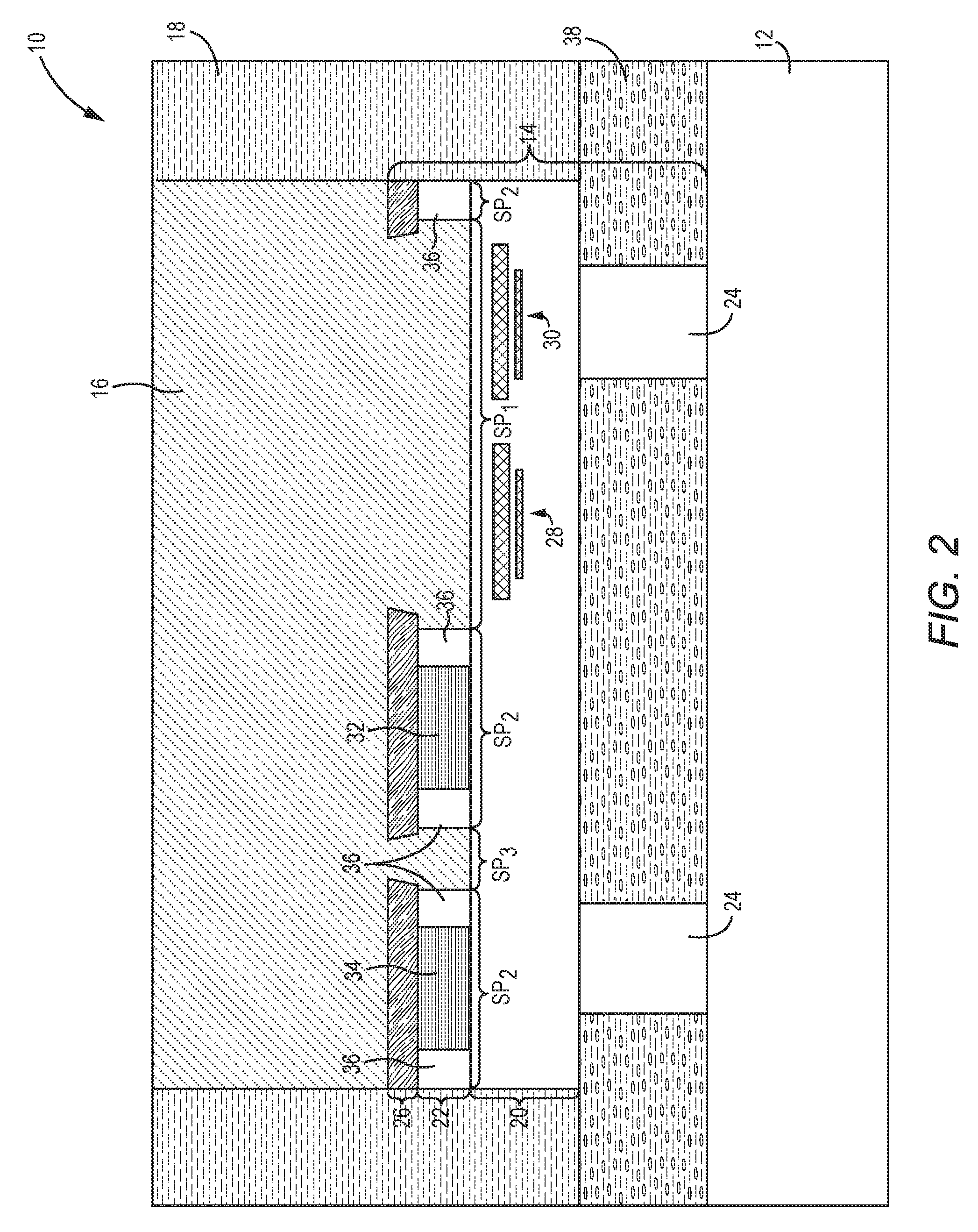
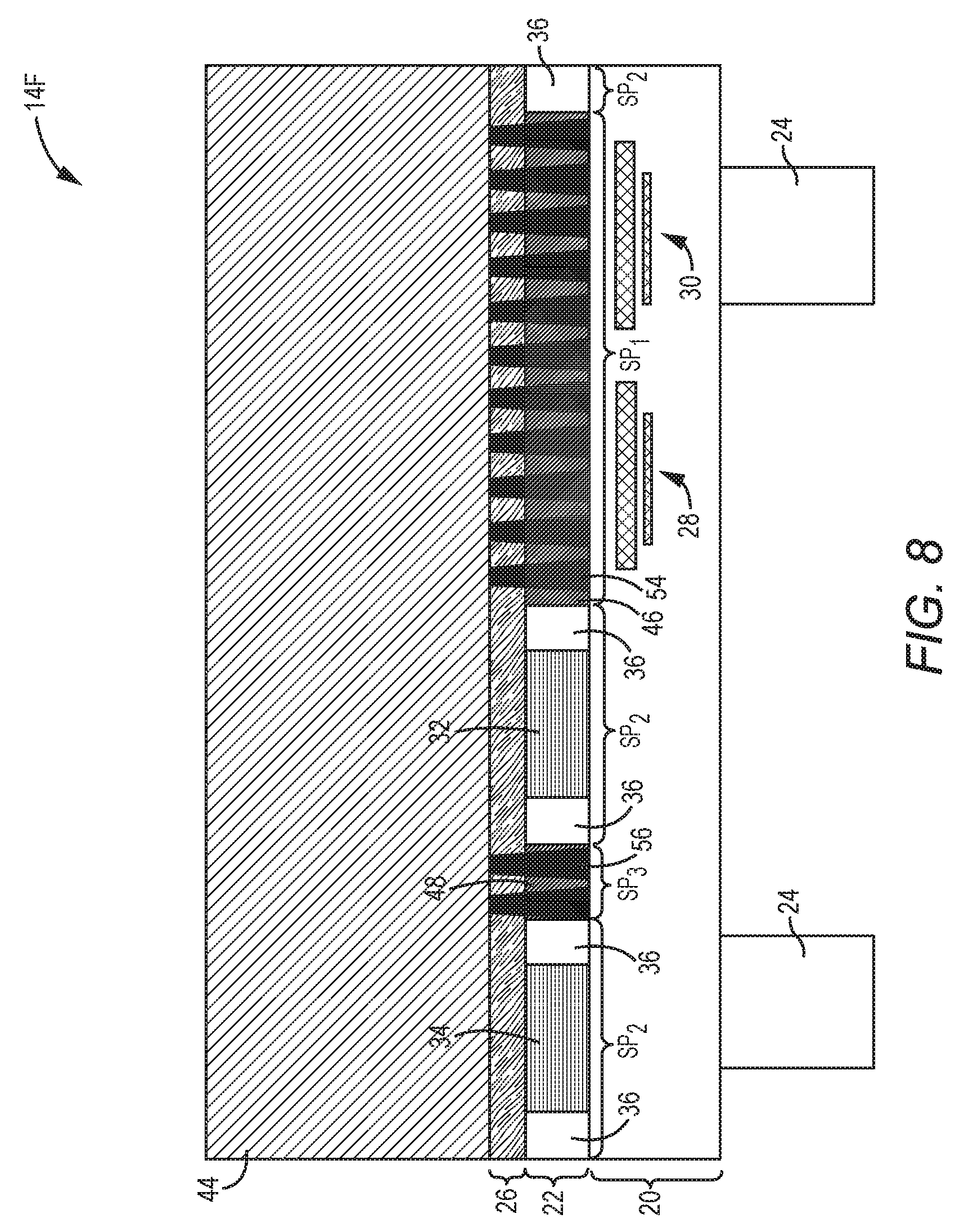
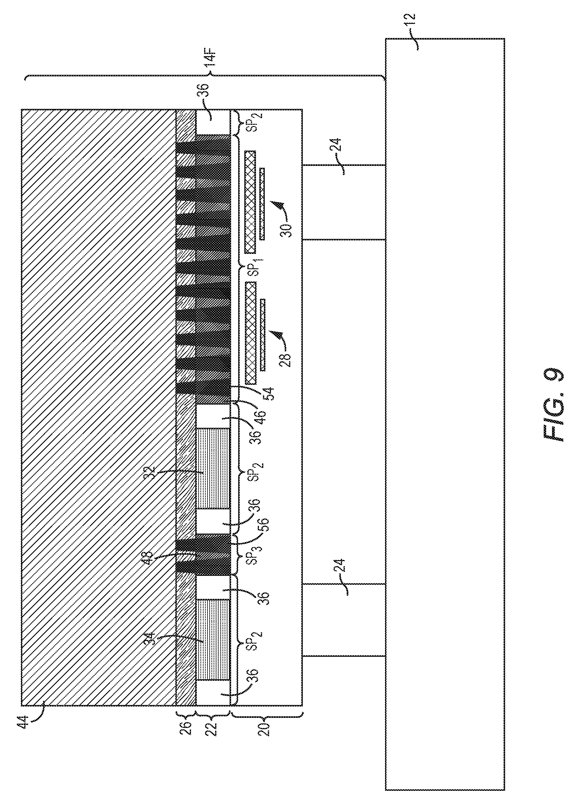
The present disclosure relates to a semiconductor package with reduced parasitic coupling effects, and a process for making the same. FIGS. 1A and 1B provide an exemplary semiconductor package 10 according to one embodiment of the present disclosure. FIG. 1A shows a cross-sectional view of the exemplary semiconductor package 10, and FIG. 1B shows a top view of the exemplary semiconductor package 10. For the purpose of this illustration, the semiconductor package 10 includes a module substrate 12, a thinned flip-chip die 14, a first mold compound component 16, and a second mold compound component 18. In different applications, the semiconductor package 10 may include multiple thinned flip-chip dies.
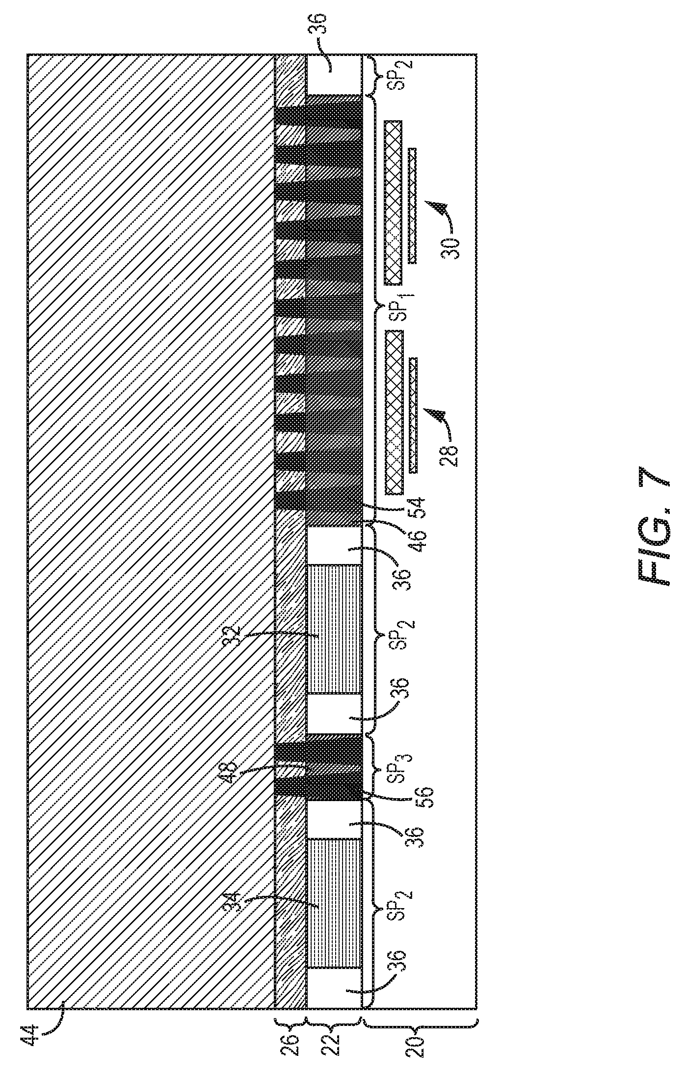
In detail, the module substrate 12 may be formed from a laminate, a wafer level fan out (WLFO) carrier, a lead frame, a ceramic carrier, or the like. The thinned flip-chip die 14 includes a back-end-of-line (BEOL) layer 20, a device layer 22 over an upper surface of the BEOL layer 20, a number of interconnects 24 extending from a lower surface of the BEOL layer 20 and coupled to an upper surface of the module substrate 12, and a buried oxide (BOX) layer 26 over the device layer 22. Herein, the upper surface of the BEOL layer 20 includes a first surface portion SP1, a second surface portion SP2, and a third surface portion SP3. The second surface portion SP2 surrounds the first surface portion SP1 and the third surface portion SP3, and the second surface portion SP2 separates the first surface portion SP1 from the third surface portion SP3.
There are a first passive device 28 and a second passive device 30 embedded in the BEOL layer 20. Both the first passive device 28 and the second passive device 30 are underlying the first surface portion SP1 and not underlying the second surface portion SP2. The device layer 22 includes a first active device 32, a second active device 34, and an isolation region 36. The first active device 32, the second active device 34, and the isolation region 36 are over the second surface portion SP2 and not over the first surface portion SP1 or the third surface portion SP3. The BOX layer 26 is over the first active device 32, the second active device 34, and the isolation region 36. In addition, the first active device 32 and the second active device 34 are located on opposite sides of the third surface portion SP3, and the first active device 32 is close to the first passive device 28. Both the first active device 32 and the second active device 34 are surrounded by the isolation region 36. The isolation region 36 may be formed by shallow trench isolation (STI). In different applications, the BEOL layer 20 may include fewer or more passive devices, the device layer 22 may include fewer or more active devices, and the configuration of the passive devices and active devices may be different. The first passive device 28 and the second passive device 30 may be metal-insulator-metal (MIM) capacitors. The first active device 32 and the second active device 34 may be field effect transistors (FET).
The first mold compound component 16 extends through the BOX layer 26 and the device layer 22 to the first surface portion SP1 and the third surface portion SP3. A portion of the first mold compound component 16 extends over at least a portion of the BOX layer 26, which is over the first active device 32 and the second active device 34. In some applications, the first mold compound component 16 resides over an entirety of the thinned flip-chip die 14. Consequently, the first mold compound component 16 resides over the first passive device 28 and the second passive device 30. Also, the first mold compound component 16 separates the first active device 32 and the second active device 34, and resides over the first active device 32 and the second active device 34. Further, the first mold compound component 16 is separated from the first active device 32 and the second active device 34 by the isolation region 36. The first mold compound component 16 may be formed from low dielectric constant materials with the dielectric constant being no more than 7 or no more than 4, such as organic thermoset and thermoplastic polymer materials, and the like.
Because the first mold compound component 16 is adjacent to the first passive device 28 and the second passive device 30, and has a dielectric constant no more than 7, a parasitic coupling effect between the first passive device 28 and the second passive device 30 is low. Most parasitic field lines between the first passive device 28 and the second passive device 30 (shown as a double arrow) close through the first mold compound component 16. Similarly, because the first mold compound component 16 is adjacent to the first active device 32 and the second active device 34 and inserted between the first active device 32 and the second active device 34, a parasitic coupling effect between the first active device 32 and the second active device 34 is low. Most parasitic field lines between the first active device 32 and the second active device 34 (shown as a double arrow) close through the first mold compound component 16. Further, a parasitic coupling effect between the first passive device 28 and the first active device 32 is low, due to the first mold compound component 16 adjacent to the first passive device 28 and the first active device 32. Most parasitic field lines between the first passive device 28 and the first active device 32 (shown as a double arrow) close through the first mold compound component 16.
The second mold compound component 18 resides over the upper surface of the module substrate 12 and encapsulates at least the sides of the first mold compound component 16 and the thinned flip-chip die 14. In some applications, a portion of the first mold compound component 16 may reside over an upper surface of the second mold compound component 18 (not shown). Herein, the second mold compound component 18 may be formed from the same or different material as the first mold compound component 16. However, unlike the first mold compound component 16, the second mold compound component 18 does not have a dielectric constant requirement in low parasitic coupling embodiments. One exemplary material used to form the second mold compound component 18 is an organic epoxy resin system.
In some applications, the semiconductor package 10 may further include an underfilling layer 38, as shown in FIG. 2. The underfilling layer 38 resides between the upper surface of the module substrate 12 and the second mold compound component 18, such that the underfilling layer 38 encapsulates the interconnects 24 and underfills the thinned flip-chip die 14 between the lower surface of the BEOL layer 20 and the upper surface of the module substrate 12. Herein, the second mold compound component 18 resides over the underfilling layer 38, and encapsulates at least the sides of the first mold compound component 16, the sides of the BOX layer 26, the sides of the device layer 22, and the sides of the BEOL layer 20. The underfilling layer 38 may be formed from the same or different material as the second mold compound component 18.
In another embodiment, as shown in FIG. 3, the semiconductor package 10 may further include a thermally enhanced mold compound component 40 that resides over the first mold compound component 16. Herein, the second mold compound component 18 further encapsulates at least the sides of the thermally enhanced mold compound component 40. In some applications, a portion of the thermally enhanced mold compound component 40 may reside over an upper surface of the second mold compound component 18 (not shown). The thermally enhanced mold compound component 40 may be formed from a thermoset or thermoplastic material. Compared to a normal mold compound component having 1 w/mk thermal conductivity, a thermally enhanced mold compound component may have 2.5 w/mk.about.50 w/mk or greater thermal conductivity. The higher the thermal conductivity, the better the heat dissipation performance of the semiconductor package 10. The thermally enhanced mold compound component 40 may be formed from the same or different material as the first mold compound component 16. However, unlike the first mold compound component 16, the thermally enhanced mold compound component 40 does not have a dielectric constant requirement in low parasitic coupling embodiments.
FIGS. 4-15 provide exemplary steps that illustrate a process to fabricate exemplary semiconductor package 10 shown in FIG. 1A. Although the exemplary steps are illustrated in a series, the exemplary steps are not necessarily order dependent. Some steps may be done in a different order than that presented. Further, processes within the scope of this disclosure may include fewer or more steps than those illustrated in FIGS. 4-15.
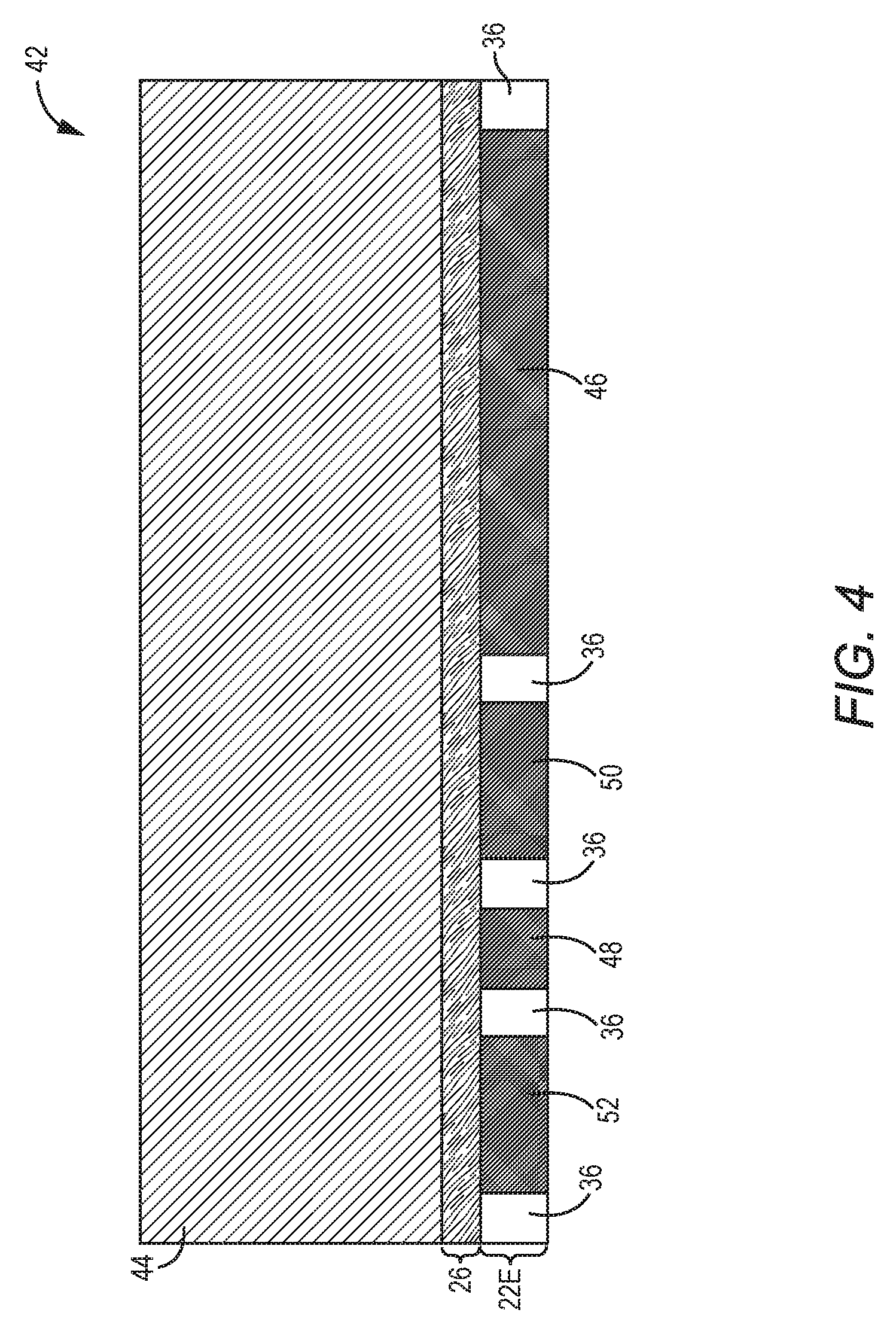
Initially, a silicon-on-insulator (SOI) structure 42 is provided as depicted in FIG. 4. The SOI structure 42 includes an epitaxy layer 22E, the BOX layer 26 over the epitaxy layer 22E, and a silicon handle layer 44 over the BOX layer 26. In detail, the epitaxy layer 22 includes a first sacrificial epitaxy section 46, a second sacrificial epitaxy section 48, a first active epitaxy section 50, a second active epitaxy section 52, and the isolation region 36. The isolation region 36 separates the first sacrificial epitaxy section 46, the second sacrificial epitaxy section 48, the first active epitaxy section 50, and the second active epitaxy section 52 from each other. The second sacrificial epitaxy section 48 is located between the first active epitaxy section 50 and the second active epitaxy section 52. The BOX layer 26 may be formed of silicon oxide or the like, which may serve as an etch stop in a process to remove the silicon handle layer 44 (more details in following discussion).
First etchable structures 54 and second etchable structures 56 are then formed as illustrated in FIG. 5A (only one first etchable structure and one second etchable structure are labeled with reference numbers for clarity). The first etchable structures 54 extend through the first sacrificial epitaxy section 46 and the BOX layer 26 to the silicon handle layer 44. In this embodiment, the first etchable structures 54 are an array configuration and distributed across the first sacrificial epitaxy section 46. The second etchable structures 56 extend through the second sacrificial epitaxy section 48 and the BOX layer 26 to the silicon handle layer 44. The second etchable structures 56 are distributed across the second sacrificial epitaxy section 48. The first etchable structures 54 and the second etchable structures 56 may be formed from polysilicon. In different applications, there may be fewer or more etchable structures extending through the sacrificial epitaxy sections. As illustrated in FIG. 5B, an alternative first etchable structure 54A that is formed through the first sacrificial epitaxy section 46 and the BOX layer 26 is a single monolithic structure.
Next, the first active device 32 and the second active device 34 are integrated in or on the epitaxy layer 22E to form a device layer 22 as illustrated in FIG. 6. The first active device 32 is formed in or on the first active epitaxy section 50 and the second active device 34 is formed in or on the second active epitaxy section 52. FIG. 7 shows forming the BEOL layer 20 under the device layer 22. The upper surface of the BEOL layer 20 is in contact with a lower surface of the device layer 22. The upper surface of the BEOL layer 20 includes the first surface portion SP1, the second surface portion SP2, and the third surface portion SP3. The second surface portion SP2 surrounds the first surface portion SP1 and the third surface portion SP3, and the second surface portion SP2 separates the first surface portion SP1 from the third surface portion SP3. Herein, the first active device 32, the second active device 34, and the isolation region 36 are over the second surface portion SP2 and not over the first surface portion SP1 or the third surface portion SP3. In addition, the BEOL layer 20 includes the first passive device 28 and the second passive device 30. Both the first passive device 28 and the second passive device 30 are underlying the first surface portion SP1 and not underlying the second surface portion SP2. Then the interconnects 24 are formed at the lower surface of the BEOL layer 20 to complete a flip-chip die 14F as illustrated in FIG. 8.
The flip-chip die 14F is then attached to the upper surface of the module substrate 12 as illustrated in FIG. 9. The interconnects 24 are extending from the lower surface of the BEOL layer 20 and coupled to the module substrate 12. Next, the second mold compound 18M is applied over the upper surface of the module substrate 12 such that the flip-chip die 14F is encapsulated by the second mold compound 18M as illustrated in FIG. 10. The second mold compound 18M may be applied by various procedures, such as sheet molding, overmolding, compression molding, transfer molding, dam fill encapsulation, and screen print encapsulation. The second mold compound 18M may be formed from an organic epoxy resin system or the like, such as Hitachi Chemical Electronic Materials GE-100LFC, which can be used as an etchant barrier to protect the flip-chip die 14F against etching chemistries such as potassium hydroxide (KOH), sodium hydroxide (NaOH), and acetylcholine (ACH). A curing process (not shown) is followed to harden the second mold compound 18M to form the second mold compound component 18. The curing temperature may be between 125.degree. C. and 300.degree. C. depending on which material is used as the second mold compound 18M.
Notice that, if the final semiconductor package 10 includes the underfilling layer 38, which is formed from a different material to the second mold compound 18M, there may be extra steps to form the underfilling layer 38 (not shown) before applying the second mold compound 18M over the upper surface of the module substrate 12. Forming the underfilling layer 38 is provided by applying an underfilling material over the upper surface of the module substrate 12 and then curing the underfilling material to form the underfilling layer 38. The underfilling layer 38 encapsulates the interconnects 24 and underfills the flip-chip die 14F between the lower surface of the BEOL layer 20 and the upper surface of the module substrate 12. The second mold compound 18M is then applied over the underfilling layer 38, and encapsulates at least the sides of the silicon handle layer 44, the sides of the BOX layer 26, the sides of the device layer 22, and the sides of the BEOL layer 20. A curing process (not shown) is followed to harden the second mold compound 18M to form the second mold compound component 18.
Next, the second mold compound component 18 is thinned down to expose the backside of the silicon handle layer 44 of the flip-chip die 14F, as shown in FIG. 11. The thinning procedure may be done with a mechanical grinding process. With reference to FIGS. 12 and 13, a process for providing the thinned flip-chip die 14 is illustrated according to one embodiment of the present disclosure. FIG. 12 shows the removal of the silicon handle layer 44, the first sacrificial epitaxy section 46, the second sacrificial epitaxy section 48, the first etchable structures 54, and the second etchable structures 56. The removing step may be provided by an etching process with a wet/dry etchant chemistry, which may be KOH, ACH, NaOH or the like. Normally, these wet/dry etchant chemistries may not etch away the BOX layer 26 and the BOX layer 26 may serve as an etch stop in the etching process. However, after removing the first etchable structures 54, a portion of the BOX layer 26 over the first surface portion SP1 includes a number of discrete and floating BOX pieces. Similarly, after removing the second etchable structures 56, another portion of the BOX layer 26 over the third surface portion SP3 may include at least one discrete and floating BOX piece. In some applications, there may be no floating BOX piece over the first surface portion SP1 or the third surface portion SP3. These discrete and floating BOX pieces can be easily removed to form the thinned flip-chip die 14 as illustrated as FIG. 13. Herein, a cavity 58 with a first extension ET1 and a second extension ET2 is formed, where the thinned flip-chip die 14 is located at the bottom of the cavity 58. The first extension ET1 of the cavity 58 extends through the BOX layer 26 and the device layer 22 to the first surface portion SP1 of the BEOL layer 20, and the second extension ET2 of the cavity 58 extends through the BOX layer 26 and the device layer 22 to the third surface portion SP3 of the BEOL layer 20.
A first mold compound 16M is then applied to substantially fill the cavity 58 as illustrated in FIG. 14. The first mold compound 16M resides over the entirety of the thinned flip-chip die 14 and extends through the BOX layer 26 and the device layer 22 to the first surface portion SP1 and the third surface portion SP3 of the BEOL layer 20. As such, the first mold compound 16M resides over the first passive device 28 and the second passive device 30. Also, the first mold compound 16M separates the first active device 32 and the second active device 34, and resides over the first active device 32 and the second active device 34. A portion of the first mold compound 16M may reside over the upper surface of the second mold compound component 18. The first mold compound 16M may be applied by various procedures, such as sheet molding, overmolding, compression molding, transfer molding, dam fill encapsulation, and screen print encapsulation. A curing process (not shown) is followed to harden the first mold compound 16M to form the first mold compound component 16. The curing temperature is between 125.degree. C. and 300.degree. C. depending on which material is used as the first mold compound 16M.
Notice that, if the final semiconductor package 10 includes the thermally enhanced mold compound component 40, which is formed over the first mold compound component 16, there may be extra steps to form the thermally enhanced mold compound component 40 (not shown) after forming the first mold compound component 16. In this embodiment, the first mold compound component 16 does not fill the entire cavity 58. Instead, the first mold compound component 16 only fills a lower region of the cavity 58. The first mold compound 16M fills the first and second extensions ET1 and ET2 of the cavity 58 and extends over at least a portion of the BOX layer 26, which is over the first active device 32 and the second active device 34. Next, a thermally enhanced mold compound 40M is applied over the first mold compound component 16 and fills an upper region of the cavity 58. A curing process (not shown) is followed to harden the thermally enhanced mold compound 40M to form the thermally enhanced mold compound component 40. Herein, the second mold compound component 18 further encapsulates at least the sides of the thermally enhanced mold compound component 40.
Finally, the upper surface of the first mold compound component 16 is planarized as illustrated in FIG. 15. A portion of the first mold compound component 16 may reside over the upper surface of the second mold compound component 18. A mechanical grinding process may be used for planarization.
Those skilled in the art will recognize improvements and modifications to the preferred embodiments of the present disclosure. All such improvements and modifications are considered within the scope of the concepts disclosed herein and the claims that follow.
* * * * *
References
-
matweb.com/search/DataSheet.aspx?MatGUID=3996a734395a4870a9739076918c4297&ckck=1
-
coolpolymers.com/dseries.asp
-
coolpolymers.com/Files/DS/Datasheet_e2.pdf
-
-
-
-
-
-
professionalplastics.com/professionalplastics/ElectricalPropertiesofPlastics.pdf
-
-
-
-
phys.huji.ac.il/Phys_Hug/Lectures/77602/PHONONS_2_thermal.pdf
-
ctherm.com/products/tci_thermal_conductivity/helpful_links_tools/thermal_resistance_thermal_conductance
-
akhansemi.com/technology.html#the-miraj-diamond-platform
-
ptonline.com/articles/plastics-that-conduct-heat
D00000
D00001
D00002
D00003
D00004
D00005
D00006
D00007
D00008
D00009
D00010
D00011
D00012
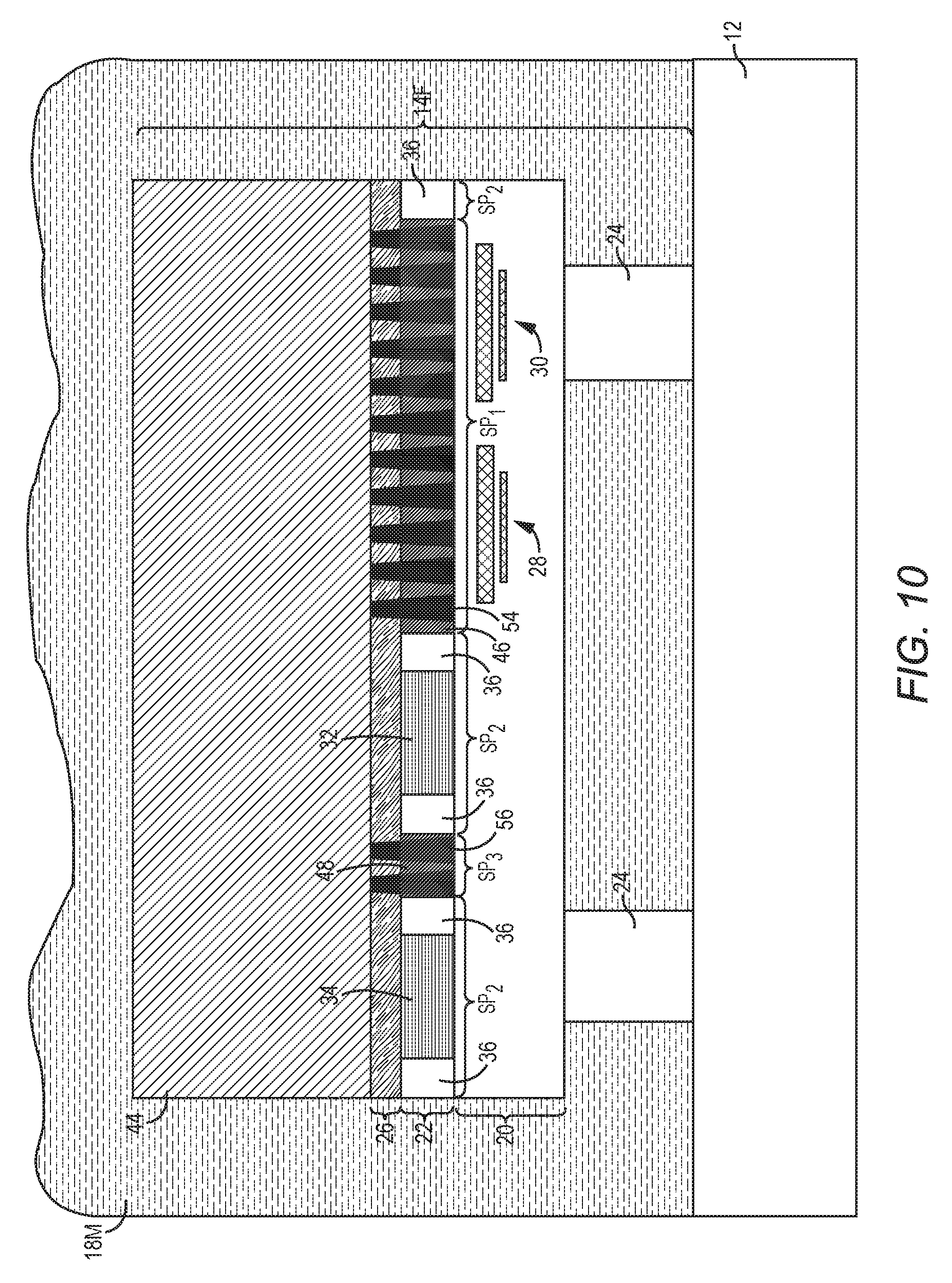
D00013
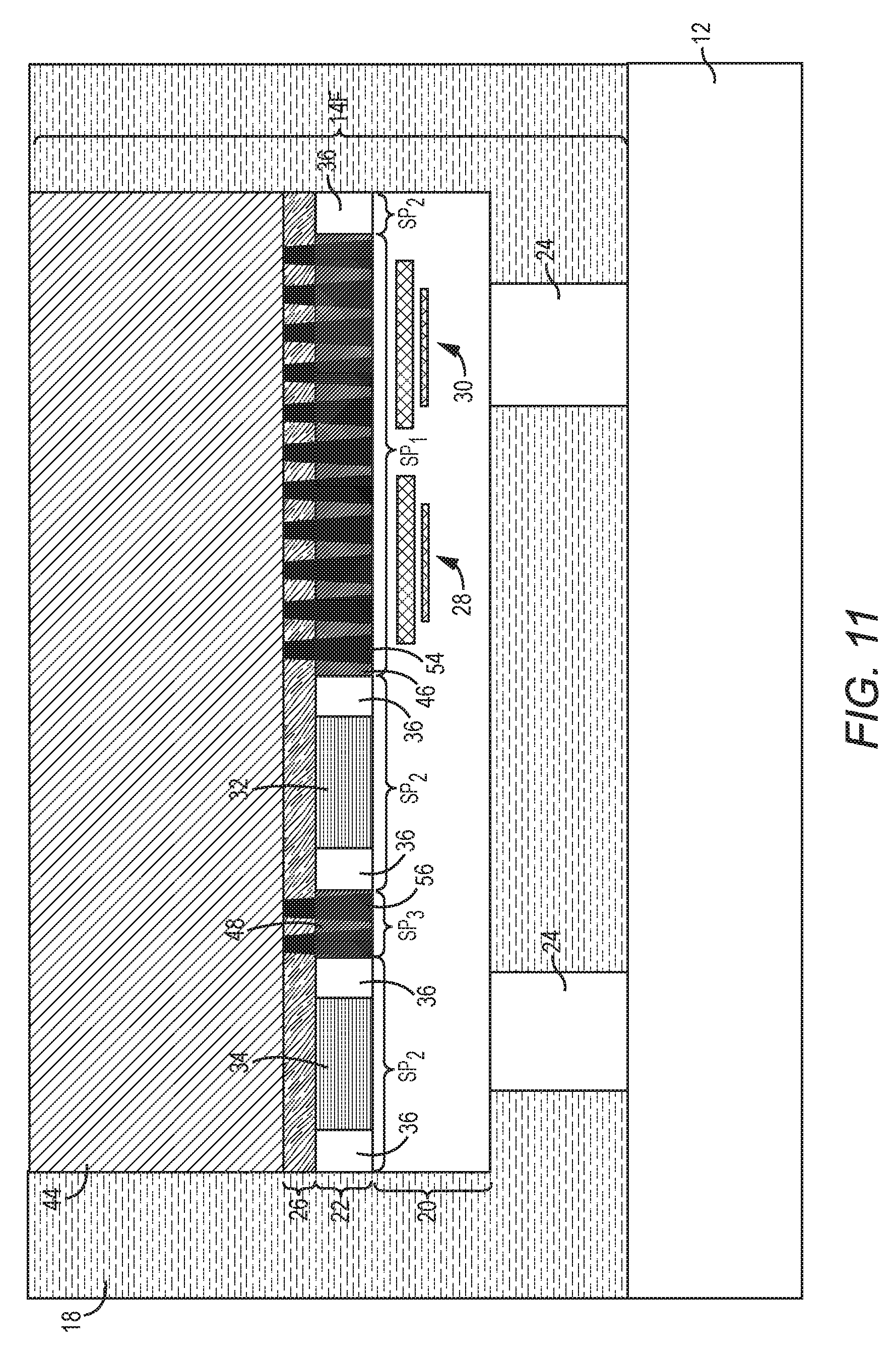
D00014

D00015
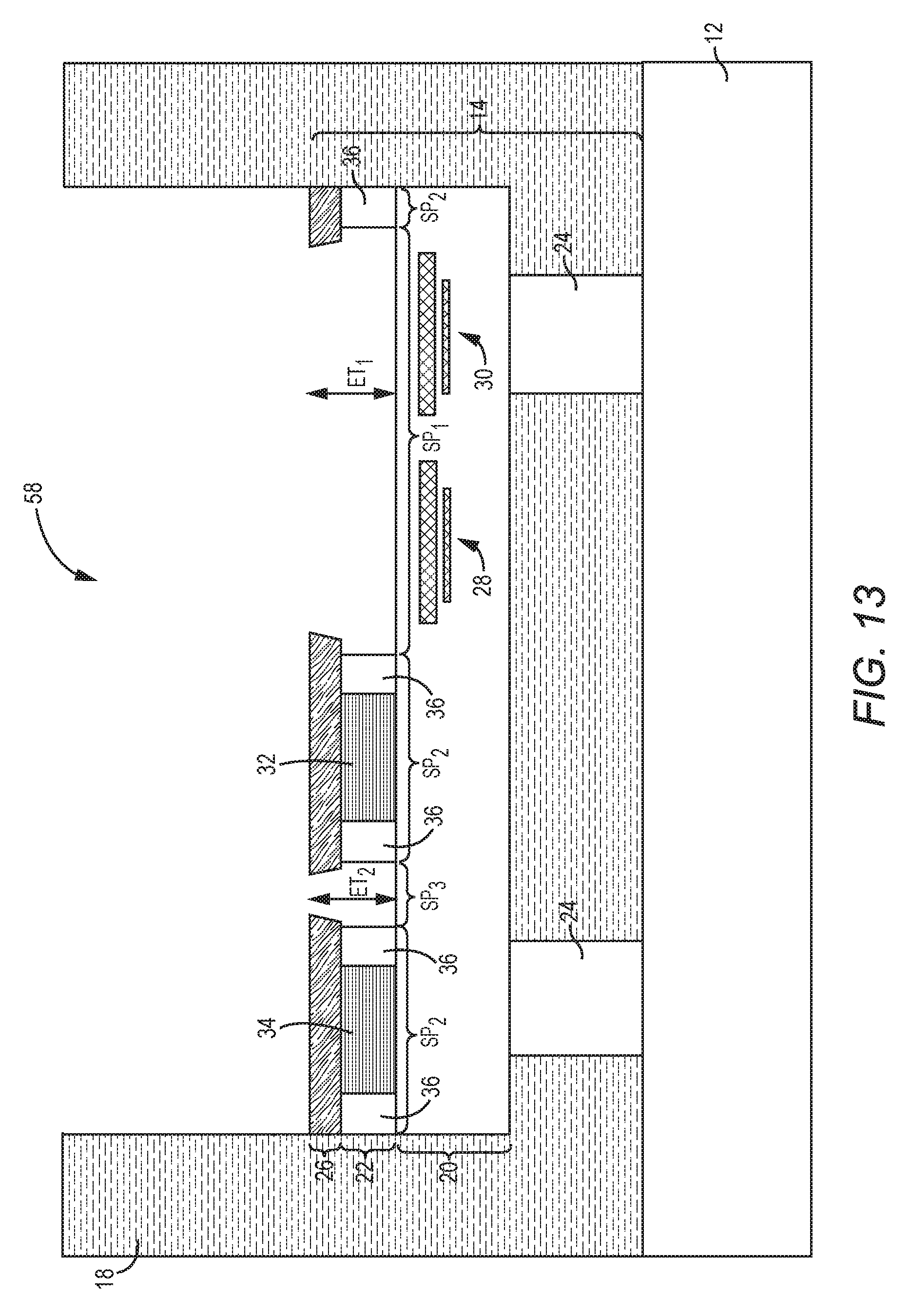
D00016
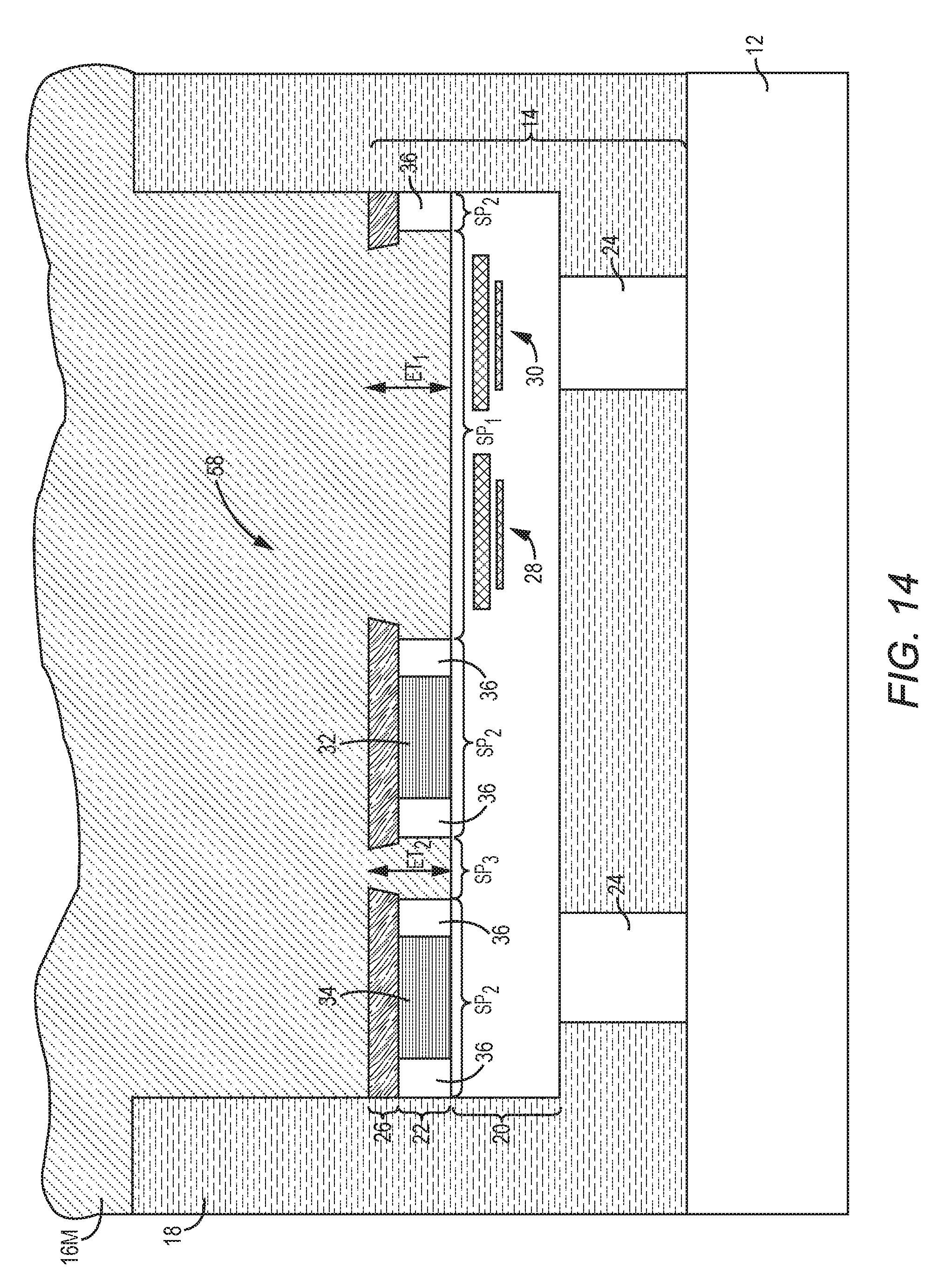
D00017

XML
uspto.report is an independent third-party trademark research tool that is not affiliated, endorsed, or sponsored by the United States Patent and Trademark Office (USPTO) or any other governmental organization. The information provided by uspto.report is based on publicly available data at the time of writing and is intended for informational purposes only.
While we strive to provide accurate and up-to-date information, we do not guarantee the accuracy, completeness, reliability, or suitability of the information displayed on this site. The use of this site is at your own risk. Any reliance you place on such information is therefore strictly at your own risk.
All official trademark data, including owner information, should be verified by visiting the official USPTO website at www.uspto.gov. This site is not intended to replace professional legal advice and should not be used as a substitute for consulting with a legal professional who is knowledgeable about trademark law.