System and method for entering and exiting sleep mode in a graphics subsystem
Jayavant , et al. October 27, 2
U.S. patent number 10,817,043 [Application Number 13/191,364] was granted by the patent office on 2020-10-27 for system and method for entering and exiting sleep mode in a graphics subsystem. This patent grant is currently assigned to NVIDIA Corporation. The grantee listed for this patent is Thomas E. Dewey, Rajeev Jayavant, David Wyatt. Invention is credited to Thomas E. Dewey, Rajeev Jayavant, David Wyatt.


| United States Patent | 10,817,043 |
| Jayavant , et al. | October 27, 2020 |
System and method for entering and exiting sleep mode in a graphics subsystem
Abstract
A technique is disclosed for a graphics processing unit (GPU) to enter and exit a power saving deep sleep mode. The technique involves preserving processing state within local memory by configuring the local memory to operate in a self-refresh mode while the GPU is powered off for deep sleep. An interface circuit coupled to the local memory is configured to prevent spurious GPU signals from disrupting proper self-refresh of the local memory. Spurious GPU signals may result from GPU power down and GPU power up events associated with the GPU entering and exiting the deep sleep mode.
| Inventors: | Jayavant; Rajeev (Sunnyvale, CA), Dewey; Thomas E. (Menlo Park, CA), Wyatt; David (San Jose, CA) | ||||||||||
|---|---|---|---|---|---|---|---|---|---|---|---|
| Applicant: |
|
||||||||||
| Assignee: | NVIDIA Corporation (Santa
Clara, CA) |
||||||||||
| Family ID: | 1000005145579 | ||||||||||
| Appl. No.: | 13/191,364 | ||||||||||
| Filed: | July 26, 2011 |
Prior Publication Data
| Document Identifier | Publication Date | |
|---|---|---|
| US 20130027413 A1 | Jan 31, 2013 | |
| Current U.S. Class: | 1/1 |
| Current CPC Class: | G06F 1/3265 (20130101); G06F 1/325 (20130101); G06F 1/3278 (20130101); Y02D 30/50 (20200801); Y02D 10/00 (20180101) |
| Current International Class: | G06T 1/00 (20060101); G06F 1/3234 (20190101) |
References Cited [Referenced By]
U.S. Patent Documents
| 4016595 | April 1977 | Compton |
| 4089058 | May 1978 | Murdock |
| 4523192 | June 1985 | Burton et al. |
| 4709195 | November 1987 | Hellekson et al. |
| 4747041 | May 1988 | Engel |
| 5255094 | October 1993 | Yong et al. |
| 5424692 | June 1995 | McDonald |
| 5475329 | December 1995 | Jones et al. |
| 5481731 | January 1996 | Conary et al. |
| 5558071 | September 1996 | Ward et al. |
| 5596765 | January 1997 | Baum |
| 5614847 | March 1997 | Kawahara et al. |
| 5623677 | April 1997 | Townsley et al. |
| 5625807 | April 1997 | Lee |
| 5628019 | May 1997 | O'Brien |
| 5630145 | May 1997 | Chen |
| 5655112 | August 1997 | MacInnis |
| 5727221 | March 1998 | Walsh |
| 5729164 | March 1998 | Pattantyus |
| 5758166 | May 1998 | Ajanovic |
| 5758170 | May 1998 | Woodward et al. |
| 5761727 | June 1998 | Wu |
| 5842029 | November 1998 | Conary et al. |
| 5844786 | December 1998 | Yoshida et al. |
| 5867717 | February 1999 | Milhaupt |
| 5896140 | April 1999 | O'Sullivan |
| 5914545 | June 1999 | Pollersbeck |
| 5935253 | August 1999 | Conary et al. |
| 5974558 | October 1999 | Cortopassi et al. |
| 5991883 | November 1999 | Atkinson |
| 6040845 | March 2000 | Melo |
| 6148356 | November 2000 | Archer |
| 6199134 | March 2001 | Deschepper |
| 6292859 | September 2001 | Santiago |
| 6418504 | July 2002 | Conway |
| 6433785 | August 2002 | Garcia |
| 6438698 | August 2002 | Hellum |
| 6466003 | October 2002 | Gallavan et al. |
| 6539486 | March 2003 | Rolls et al. |
| 6557065 | April 2003 | Peleg |
| 6581115 | June 2003 | Arimilli |
| 6604161 | August 2003 | Miller |
| 6622178 | September 2003 | Burke |
| 6691236 | February 2004 | Atkinson |
| 6711691 | March 2004 | Howard |
| 6717451 | April 2004 | Klein et al. |
| 6785829 | August 2004 | George et al. |
| 6807629 | October 2004 | Billick |
| 6895456 | May 2005 | Olarig |
| 6963340 | November 2005 | Alben et al. |
| 6985152 | January 2006 | Rubinstein |
| 7054964 | May 2006 | Chan |
| 7058829 | June 2006 | Hamilton |
| 7136953 | November 2006 | Bisson |
| 7426597 | September 2008 | Tsu |
| 7456833 | November 2008 | Diard |
| 7469311 | December 2008 | Tsu |
| 7548481 | June 2009 | Dewey et al. |
| 7598959 | October 2009 | Kardach |
| 7624221 | November 2009 | Case |
| 7698489 | April 2010 | Jacoby |
| 7800621 | September 2010 | Fry |
| 7802118 | September 2010 | Abdalla et al. |
| 7827424 | November 2010 | Bounitch |
| 7925907 | April 2011 | Reed |
| 7958483 | June 2011 | Alben |
| 8040351 | October 2011 | Diard |
| 8095813 | January 2012 | Pernia et al. |
| 8255708 | August 2012 | Zhang |
| 8325184 | December 2012 | Jiao |
| 8352644 | January 2013 | Malamant |
| 8392695 | March 2013 | Lachwani et al. |
| 8621253 | December 2013 | Brown |
| 8635480 | January 2014 | Mimberg |
| 8717371 | May 2014 | Wyatt |
| 8762748 | June 2014 | Zhang |
| 8928907 | January 2015 | Min |
| 8941672 | January 2015 | Jacoby |
| 8943347 | January 2015 | Khodorkovsky |
| 9047085 | June 2015 | Wyatt |
| 9098259 | August 2015 | Lachwani |
| 9342131 | May 2016 | Saito |
| 9619005 | April 2017 | No |
| 9625976 | April 2017 | Zhang |
| 10365706 | July 2019 | Bakshi |
| 2002/0060640 | May 2002 | Davis et al. |
| 2002/0062416 | May 2002 | Kim |
| 2002/0099980 | July 2002 | Olarig |
| 2002/0109688 | August 2002 | Olarig |
| 2002/0194548 | December 2002 | Tetreault |
| 2003/0097495 | May 2003 | Hansen |
| 2003/0182487 | September 2003 | Dennis |
| 2003/0229403 | December 2003 | Nakazawa et al. |
| 2003/0233588 | December 2003 | Verdun |
| 2004/0024941 | February 2004 | Olarig et al. |
| 2004/0138833 | July 2004 | Flynn |
| 2004/0143776 | July 2004 | Cox |
| 2004/0155636 | August 2004 | Fukui et al. |
| 2004/0250035 | December 2004 | Atkinson |
| 2005/0030311 | February 2005 | Hara |
| 2005/0060468 | March 2005 | Emerson |
| 2005/0133932 | June 2005 | Pohl et al. |
| 2005/0148358 | July 2005 | Lin |
| 2005/0151082 | July 2005 | Coffin et al. |
| 2005/0231454 | October 2005 | Alben et al. |
| 2005/0259106 | November 2005 | Rai |
| 2005/0289377 | December 2005 | Luong |
| 2006/0020835 | January 2006 | Samson |
| 2006/0054610 | March 2006 | Morimoto et al. |
| 2006/0089819 | April 2006 | Dubal |
| 2006/0106911 | May 2006 | Chapple |
| 2006/0112287 | May 2006 | Paljug |
| 2006/0145328 | July 2006 | Hsu |
| 2006/0170098 | August 2006 | Hsu |
| 2006/0212733 | September 2006 | Hamilton |
| 2006/0236027 | October 2006 | Jain et al. |
| 2006/0245287 | November 2006 | Seitz et al. |
| 2006/0259801 | November 2006 | Chu |
| 2006/0259804 | November 2006 | Fry |
| 2006/0287805 | December 2006 | Enomoto et al. |
| 2007/0005995 | January 2007 | Kardach |
| 2007/0094486 | April 2007 | Moore et al. |
| 2007/0143640 | June 2007 | Simeral |
| 2007/0201173 | August 2007 | Chu et al. |
| 2007/0212103 | September 2007 | Kikuchi |
| 2007/0296613 | December 2007 | Hussain |
| 2007/0297501 | December 2007 | Hussain |
| 2007/0300207 | December 2007 | Booth et al. |
| 2008/0048755 | February 2008 | Cho et al. |
| 2008/0117222 | May 2008 | Leroy |
| 2008/0143731 | June 2008 | Cheng |
| 2008/0168201 | July 2008 | de Cesare |
| 2008/0168285 | July 2008 | de Cesare |
| 2008/0180564 | July 2008 | Yamaji |
| 2008/0263315 | October 2008 | Zhang |
| 2008/0309355 | December 2008 | Nozaki et al. |
| 2009/0041380 | February 2009 | Watanabe |
| 2009/0073168 | March 2009 | Jiao |
| 2009/0077307 | March 2009 | Kaburlasos et al. |
| 2009/0079746 | March 2009 | Howard et al. |
| 2009/0096797 | April 2009 | Du et al. |
| 2009/0100279 | April 2009 | Lee |
| 2009/0153211 | June 2009 | Hendin et al. |
| 2009/0153540 | June 2009 | Blinzer et al. |
| 2009/0193234 | July 2009 | Ors et al. |
| 2009/0204766 | August 2009 | Jacobi et al. |
| 2009/0204831 | August 2009 | Cousson |
| 2009/0204834 | August 2009 | Hendin et al. |
| 2009/0204835 | August 2009 | Smith et al. |
| 2009/0204837 | August 2009 | Raval et al. |
| 2009/0207147 | August 2009 | Perrot |
| 2009/0240892 | September 2009 | Moyer |
| 2009/0259982 | October 2009 | Verbeure |
| 2010/0007646 | January 2010 | Tsuei |
| 2010/0031071 | February 2010 | Lu |
| 2010/0058089 | March 2010 | Lerman |
| 2010/0064125 | March 2010 | Liu et al. |
| 2010/0088453 | April 2010 | Solki |
| 2010/0123725 | May 2010 | Azar |
| 2010/0127407 | May 2010 | LeBlanc et al. |
| 2010/0148316 | June 2010 | Kim et al. |
| 2010/0157713 | June 2010 | Furutani |
| 2010/0177070 | July 2010 | Zhu et al. |
| 2010/0201340 | August 2010 | Raghavan |
| 2010/0220102 | September 2010 | Wyatt et al. |
| 2010/0281185 | November 2010 | Takayama |
| 2010/0309704 | December 2010 | Dattaguru et al. |
| 2011/0029694 | February 2011 | Blinzer |
| 2011/0047326 | February 2011 | Kaburlasos et al. |
| 2011/0053649 | March 2011 | Wilson |
| 2011/0057936 | March 2011 | Gotwalt |
| 2011/0060928 | March 2011 | Khodorkovsky |
| 2011/0109371 | May 2011 | Kastl |
| 2011/0143809 | June 2011 | Salomone |
| 2011/0148890 | June 2011 | Kaburlasos |
| 2011/0157191 | June 2011 | Huang |
| 2011/0169840 | July 2011 | Bakalash |
| 2011/0173476 | July 2011 | Reed |
| 2011/0185208 | July 2011 | Iwamoto |
| 2011/0215836 | September 2011 | Shimizu |
| 2011/0216780 | September 2011 | Zhu |
| 2011/0221417 | September 2011 | Ishidoh et al. |
| 2011/0221757 | September 2011 | Hsieh |
| 2011/0252200 | October 2011 | Hendry |
| 2011/0264902 | October 2011 | Hollingworth et al. |
| 2011/0285208 | November 2011 | Xiao |
| 2012/0008431 | January 2012 | Lee |
| 2012/0079302 | March 2012 | Ise |
| 2012/0133659 | May 2012 | Masnikosa |
| 2012/0151264 | June 2012 | Balkan et al. |
| 2012/0204043 | August 2012 | Hamasaki |
| 2012/0206461 | August 2012 | Wyatt |
| 2012/0207208 | August 2012 | Wyatt |
| 2012/0236013 | September 2012 | Wyatt |
| 2012/0242671 | September 2012 | Wyatt |
| 2012/0242672 | September 2012 | Larson |
| 2012/0248875 | October 2012 | Fang |
| 2012/0249559 | October 2012 | Khodorkovsky |
| 2012/0249563 | October 2012 | Wyatt |
| 2012/0286881 | November 2012 | Mahooti et al. |
| 2012/0317607 | December 2012 | Wyatt |
| 2013/0002596 | January 2013 | Ke |
| 2013/0007492 | January 2013 | Sokol, Jr. |
| 2013/0021352 | January 2013 | Wyatt |
| 2013/0027413 | January 2013 | Jayavant |
| 2013/0038615 | February 2013 | Hendry |
| 2013/0063607 | March 2013 | Shimotono |
| 2013/0069964 | March 2013 | Wuu |
| 2013/0083047 | April 2013 | Shamarao |
| 2013/0111092 | May 2013 | Heller |
| 2013/0111242 | May 2013 | Heller |
| 2013/0151881 | June 2013 | Chen |
| 2013/0159741 | June 2013 | Schluessler |
| 2013/0159750 | June 2013 | Branover |
| 2013/0194286 | August 2013 | Bourd |
| 2013/0198548 | August 2013 | No |
| 2013/0235053 | September 2013 | Bourd |
| 2013/0265307 | October 2013 | Goel |
| 2013/0318278 | November 2013 | Wu |
| 2013/0332764 | December 2013 | Juang |
| 2013/0346640 | December 2013 | Gui |
| 2014/0092103 | April 2014 | Saulters |
| 2014/0092109 | April 2014 | Saulters |
| 2014/0181806 | June 2014 | Abiezzi |
| 2014/0181807 | June 2014 | Fonseca |
| 2014/0184629 | July 2014 | Wyatt |
| 2014/0232731 | August 2014 | Holland |
| 2014/0258738 | September 2014 | Greenwalt |
| 2014/0344599 | November 2014 | Branover |
| 2014/0380028 | December 2014 | Cheng |
| 2015/0153818 | June 2015 | Jeon |
| 2015/0193062 | July 2015 | Wyatt |
| 2015/0194137 | July 2015 | Wyatt |
| 2015/0379670 | December 2015 | Koker |
| 2016/0150130 | May 2016 | Noro |
| 2016/0209900 | July 2016 | Blayvas |
| 2016/0292812 | October 2016 | Wu |
| 2016/0370844 | December 2016 | Kumar |
| 2016/0378709 | December 2016 | Menachem |
| 2017/0061568 | March 2017 | Metz |
| 2017/0154005 | June 2017 | Ahmed |
| 2017/0199542 | July 2017 | Sylvester |
| 2017/0277643 | September 2017 | Zhou |
| 2018/0232034 | August 2018 | DiBene, II |
| 2018/0293205 | October 2018 | Koker |
| 2019/0056955 | February 2019 | Pennala |
| 2019/0235615 | August 2019 | Shows |
| 2019/0303322 | October 2019 | Sharma |
| 2020/0135151 | April 2020 | Jiang |
| 1229710 | Nov 2005 | CN | |||
| 1983329 | Jun 2007 | CN | |||
| 1 951 015 | Jul 2008 | EP | |||
| 200923784 | Jun 2009 | TW | |||
| 2008067258 | Jun 2008 | WO | |||
Other References
|
Search and Examination Report from the UK Intellectual Property Office dated Oct. 31, 2012. cited by applicant. |
Primary Examiner: Beard; Charles L
Attorney, Agent or Firm: Artegis Law Group, LLP
Claims
What is claimed is:
1. A method implemented by a graphics processing unit (GPU) for entering and exiting sleep mode, the method comprising: receiving a command for the GPU to enter a sleep mode; and in response to receiving the command for the GPU to enter the sleep mode, performing the steps of: saving an internal processing state of the GPU to a memory system local to the GPU; causing at least one enable signal used for controlling transmission of data between the GPU and the memory system to be clamped to a fixed voltage prior to entering a power-down state; causing a first communications bus that couples the GPU to a central processing unit (CPU) to be disabled; causing at least one memory device included in the memory system to enter a self-refresh mode; transmitting a signal to an embedded controller to enable a second communications bus that couples the embedded controller to the GPU; and entering the power-down state.
2. The method of claim 1, further comprising stalling all incoming workloads and completing all in-progress processing in order to halt processing within the GPU.
3. The method of claim 1, wherein the at least one memory device comprises a dynamic random access memory (DRAM) device, and the step of saving comprises copying the internal processing state for the GPU to the DRAM device.
4. The method of claim 1, wherein the at least one memory device comprises a non-volatile memory, and the step of saving comprises copying the internal processing state for the GPU and a memory interface state to the non-volatile memory.
5. The method of claim 4, wherein the non-volatile memory comprises at least one flash memory device coupled to the GPU via an interface that is independent of an interface to a different memory device within the memory system.
6. The method of claim 1, wherein the GPU and memory system are configured to operate at a predetermined speed and operating state prior to entering the power-down state.
7. The method of claim 1, further comprising: entering a power-on state; determining that the power-on state is associated with the sleep mode; causing the at least one memory device included in the memory system to exit the self-refresh mode; reloading the internal processing state for the GPU from the memory system to the GPU.
8. The method of claim 7, further comprising performing a power-on reset of the GPU and detecting a warm-boot state for transitioning the GPU from the power-down state to the power-on state.
9. The method of claim 7, wherein the at least one memory device comprises a DRAM device, and the step of reloading comprises copying the internal processing state for the GPU from the DRAM device to the GPU.
10. The method of claim 9, wherein the at least one memory device comprises a non-volatile memory device, and the step of reloading comprises copying the internal processing state for the GPU and a DRAM interface state from the non-volatile memory device to the GPU.
11. The method of claim 10, wherein the non-volatile memory device comprises at least one flash memory device, coupled to the GPU via an interface that is independent of the DRAM device.
12. The method of claim 7, wherein the GPU and the memory system are configured to operate at a predetermined speed and operating state prior to entering the power-on state.
13. The method of claim 7, further comprising causing at least one enable signal used for controlling transmission of data between the GPU and the memory system to be clamped to a fixed voltage prior to exiting the power-on state.
14. The method of claim 10, wherein a portion of the internal processing state for the GPU and the DRAM interface state are restored to a previously configured state based on data stored within the non-volatile memory.
15. The method of claim 1, wherein the CPU is configured to communicate with the GPU when the first communications bus is disabled.
16. The method of claim 1, wherein the CPU is configured to notify the GPU of cursor updates and screen refreshes when the first communications bus is disabled.
17. A non-transitory computer-readable storage medium including instructions that, when executed by a graphics processing unit (GPU), cause the GPU to enter and exit a sleep mode, by performing the steps of: receiving a command for the GPU to enter a sleep mode; and in response to receiving the command for the GPU to enter the sleep mode, performing the steps of: saving an internal processing state of the GPU to a memory system local to the GPU; causing at least one enable signal used for controlling transmission of data between the GPU and the memory system to be clamped to a fixed voltage prior to entering a power-down state; causing a first communications bus that couples the GPU to a central processing unit (CPU) to be disabled; causing at least one memory device included in the memory system to enter a self-refresh mode; transmitting a signal to an embedded controller to enable a second communications bus that couples the embedded controller to the GPU; and entering the power-down state.
18. The non-transitory computer-readable storage medium of claim 17, further comprising stalling all incoming workloads and completing all in-progress processing in order to halt processing within the GPU.
19. The non-transitory computer-readable storage medium of claim 17, wherein the at least one memory device comprises a dynamic random access memory (DRAM) device, and the step of saving comprises copying the internal processing state for the GPU to the DRAM device.
20. The non-transitory computer-readable storage medium of claim 17, wherein the at least one memory device comprises a non-volatile memory, and the step of saving comprises copying the internal processing state for the GPU and a memory interface state to the non-volatile memory.
21. The non-transitory computer-readable storage medium of claim 20, wherein the non-volatile memory comprises at least one flash memory device coupled to the GPU via an interface that is independent of an interface to a different memory device within the memory system.
22. The non-transitory computer-readable storage medium of claim 17, wherein the GPU and memory system are configured to operate at a predetermined speed and operating state prior to entering the power-down state.
23. The non-transitory computer-readable storage medium of claim 17, further comprising: entering a power-on state; determining that the power-on state is associated with the sleep mode; causing the at least one memory device included in the memory system to exit the self-refresh mode; reloading the internal processing state for the GPU from the memory system to the GPU.
24. The non-transitory computer-readable storage medium of claim 23, further comprising performing a power-on reset of the GPU and detecting a warm-boot state for transitioning the GPU from the power-down state to the power-on state.
25. The non-transitory computer-readable storage medium of claim 23, wherein the at least one memory device comprises a DRAM device, and the step of reloading comprises copying the internal processing state for the GPU from the DRAM device to the GPU.
26. The non-transitory computer-readable storage medium of claim 25, wherein the at least one memory device comprises a non-volatile memory device, and the step of reloading comprises copying the internal processing state for the GPU and a DRAM interface state from the non-volatile memory device to the GPU.
27. The non-transitory computer-readable storage medium of claim 26, wherein the non-volatile memory device comprises at least one flash memory device, coupled to the GPU via an interface that is independent of the DRAM device.
28. The non-transitory computer-readable storage medium of claim 23, wherein the GPU and the memory system are configured to operate at a predetermined speed and operating state prior to entering the power-on state.
29. The non-transitory computer-readable storage medium of claim 23, further comprising causing at least one enable signal used for controlling transmission of data between the GPU and the memory system to be clamped to a fixed voltage prior to exiting the power-on state.
30. The non-transitory computer-readable storage medium of claim 26, wherein a portion of the internal processing state for the GPU and the DRAM interface state are restored to a previously configured state based on data stored within the non-volatile memory.
31. A computing device, comprising: a memory system configured to operate in an active mode and a low power self-refresh mode; an isolation circuit coupled to the memory system and configured to cause at least one enable signal used for controlling transmission of data between a graphics processing unit (GPU) and the memory system to be clamped to a fixed voltage prior to entering a power-down state; the GPU coupled to the memory system and to the isolation circuit and configured to: receive a command for the GPU to enter a sleep mode; and in response to receiving the command for the GPU to enter the sleep mode, performing the steps of: save an internal processing state of the GPU to the memory system; cause a first communications bus that couples the GPU to a central processing unit (CPU) to be disabled; cause at least one memory device included in the memory system to enter a self-refresh mode; transmit a signal to an embedded controller to enable a second communications bus that couples the embedded controller to the GPU; enter the power-down state; enter a power-on state; determine that the power-on state is associated with a sleep mode; cause the first communications bus to be enabled; cause the at least one memory device included in the memory system to exit the self-refresh mode; and load the internal processing state for the GPU from the memory system to the GPU.
Description
BACKGROUND OF THE INVENTION
Field of the Invention
The invention relates generally to graphics processing systems and, more specifically, to a system and method for entering and exiting sleep mode in a graphics subsystem.
Description of the Related Art
Certain computer systems include a graphics processing unit (GPU) configured to perform computational tasks in cooperation with a central processing unit (CPU). During normal operation, the GPU may be assigned the computational tasks as needed. Data and program code related to the computational tasks are conventionally stored within a local memory system comprising one or more memory devices. Certain state information related to the computational tasks may be stored on the GPU. Between performing the computational tasks, the GPU may remain idle for predictable spans of time. During a span of idle time, the GPU may be put in a sleep mode to reduce power consumption. One type of sleep mode involves gating off a primary clock signal to one or more clock domains within the GPU. Gating off the primary clock signal can beneficially reduce dynamic power consumption. However, modern fabrication technology that enables the manufacture of advanced GPU devices with extremely dense circuitry inevitably introduces significant static power dissipation, which is present whenever the GPU device is powered on.
To address static power dissipation during spans of idle time, a second sleep mode, referred to herein as a deep sleep mode, involves actually shutting off power to the GPU. The deep sleep mode further reduces average power consumption by eliminating both dynamic and static power consumption associated with portions of the GPU circuitry that enter the deep sleep mode.
Prior to entering the deep sleep mode, operating state information for the GPU needs to be saved to system memory, which is configured to preserve the operating state information, which may include certain contents of the local memory as well as certain portions of internal GPU state. The operating state information needs to be restored within the GPU and local memory prior to the GPU resuming operation and immediately following an exit from the deep sleep mode. Each time the GPU is conventionally put into deep sleep, the operating state information is transmitted to a main memory associated with the CPU. Each time the GPU conventionally exists deep sleep, the operating state information is transmitted from the main memory to the GPU and local memory. Entering and exiting deep sleep involves transmitting significant amounts of state information between system memory and the GPU. As a consequence, use of the deep sleep mode can be very time consuming and lead to overall system performance degradation.
As the foregoing illustrates, what is needed in the art is an improved technique for entering and exiting a deep sleep mode in a graphics processing unit.
SUMMARY OF THE INVENTION
One embodiment of the present invention sets forth a method implemented by a graphics processing unit (GPU) for entering and exiting sleep mode. The method includes receiving a command to enter a sleep mode, saving internal processing state for the GPU to a memory system local to the GPU, causing at least one memory device included in the memory system to enter a self-refresh mode, and entering a power-down state.
Another embodiment of the present invention sets forth a computer-readable storage medium including instructions that, when executed by a processor, cause the processor to perform the method steps set forth above. Yet another embodiment of the present invention sets forth a computing device configured to implement the method steps set forth above.
One advantage of the disclosed technique is that a GPU may efficiently enter and exit a deep sleep power saving mode by leveraging low power self-refresh modes available from locally attached memory. By contrast, prior art systems do not benefit from maintaining GPU context within local memory.
BRIEF DESCRIPTION OF THE DRAWINGS
So that the manner in which the above recited features of the invention can be understood in detail, a more particular description of the invention, briefly summarized above, may be had by reference to embodiments, some of which are illustrated in the appended drawings. It is to be noted, however, that the appended drawings illustrate only typical embodiments of this invention and are therefore not to be considered limiting of its scope, for the invention may admit to other equally effective embodiments.
FIG. 1 is a block diagram illustrating a computer system configured to implement one or more aspects of the present invention;
FIG. 2 illustrates communication signals between a parallel processing subsystem and various components of the computer system, according to one embodiment of the present invention;
FIG. 3A is a detailed illustration of an external conditioning circuit, according to one embodiment of the present invention;
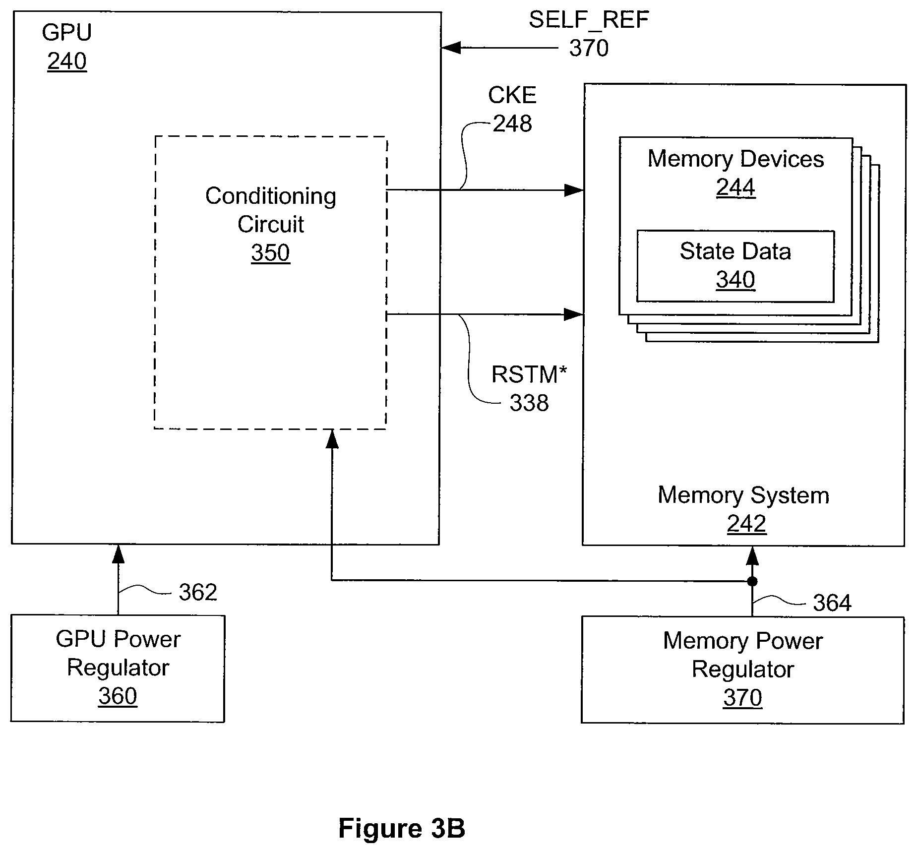
FIG. 3B is a detailed illustration of an integrated conditioning circuit, according to one embodiment of the present invention;
FIG. 4A sets forth a flowchart of method steps for causing the parallel processing system to enter a deep sleep state, according to one embodiment of the present invention; and
FIG. 4B sets forth a flow chart of method steps for causing the parallel processing system to exit the deep sleep state, according to one embodiment of the present invention.
DETAILED DESCRIPTION
In the following description, numerous specific details are set forth to provide a more thorough understanding of the invention. However, it will be apparent to one of skill in the art that the invention may be practiced without one or more of these specific details. In other instances, well-known features have not been described in order to avoid obscuring the invention.
System Overview
FIG. 1 is a block diagram illustrating a computer system 100 configured to implement one or more aspects of the present invention. Computer system 100 includes a central processing unit (CPU) 102 and a system memory 104 configured to communicate via an interconnection path that may include a memory bridge 105. Memory bridge 105, which may be, e.g., a Northbridge chip, is connected via a bus or other communication path 106 (e.g., a HyperTransport link) to an I/O (input/output) bridge 107. I/O bridge 107, which may be, e.g., a Southbridge chip, receives user input from one or more user input devices 108 (e.g., keyboard, mouse) and forwards the input to CPU 102 via communications path 106 and memory bridge 105. A parallel processing subsystem 112 is coupled to memory bridge 105 via a bus or other communication path 113 (e.g., a PCI Express, Accelerated Graphics Port, or HyperTransport link). In one embodiment parallel processing subsystem 112 is a graphics subsystem that delivers pixels to a display device 110 (e.g., a conventional CRT or LCD based monitor). A parallel processing subsystem, driver 103 is configured to manage the parallel processing subsystem 112. The parallel processing subsystem driver 103 may be configured to send graphics primitives over communication path 113 for parallel processing subsystem 112 to generate pixel data for display on display device 110. A system disk 114 is also connected to I/O bridge 107. A switch 116 provides connections between I/O bridge 107 and other components such as a network adapter 118 and various add-in cards 120 and 121.
An embedded controller 150 is coupled to the parallel processing subsystem 112. In one embodiment, the embedded controller 150 is also coupled to the CPU 102 via an interconnect path that may include the memory bridge 105. Alternatively, the embedded controller 150 is coupled to the CPU 102 via the I/O bridge 107. As described in greater detail below, embedded controller 150 is configured to manage certain operational aspects of the parallel processing subsystem 112.
Other components (not explicitly shown), including universal serial bus (USB) connections or other port connections, CD drives, DVD drives, film recording devices, and the like, may also be connected to either the memory bridge 105, or the I/O bridge 107. Communication paths interconnecting the various components in FIG. 1 may be implemented using any suitable protocols, such as PCI (Peripheral Component Interconnect), PCI-Express, AGP (Accelerated Graphics Port), HyperTransport, or any other bus or point-to-point communication protocol(s). The connections between different devices may use any technically feasible protocols.
In one embodiment, the parallel processing subsystem 112 incorporates circuitry optimized for graphics and video processing, including, for example, video output circuitry, and constitutes a graphics processing unit (GPU). In another embodiment, the parallel processing subsystem 112 may be integrated with one or more other system elements, such as the memory bridge 105, CPU 102, and I/O bridge 107 to form a system on chip (SoC).
It will be appreciated that the system shown herein is illustrative and that variations and modifications are possible. The connection topology, including the number and arrangement of bridges, the number of CPUs 102, and the number of parallel processing subsystems 112, may be modified as needed for a specific implementation. For instance, in some embodiments, system memory 104 is connected to CPU 102 directly rather than through a bridge, and other devices communicate with system memory 104 via memory bridge 105 and CPU 102. In other alternative topologies, parallel processing subsystem 112 is connected to I/O bridge 107 or directly to CPU 102, rather than to memory bridge 105. In still other embodiments, I/O bridge 107 and memory bridge 105 are integrated into a single chip. Certain embodiments may include two or more CPUs 102 and two or more parallel processing systems 112. The particular components shown herein are optional; for instance, any number of add-in cards or peripheral devices might be supported. In some embodiments, switch 116 is eliminated, and network adapter 118 and add-in cards 120, 121 connect directly to I/O bridge 107.
FIG. 2 illustrates communication signals between parallel processing subsystem 112 and various components of computer system 100, according to one embodiment of the present invention. A detail of computer system 100 is shown, illustrating the embedded controller (EC) 150, an SPI flash device 256, a system basic input/output system (SBIOS) 252, and the driver 103. EC 150 may be an embedded controller that implements an advanced configuration and power interface (ACPI) that allows an operating system executing on CPU 102 to configure and control the power management of various components of computer system 100. In one embodiment, EC 150 allows the operating system executing on CPU 102 to communicate with GPU 240 via driver 103 even when the communications path 113 is disabled. In one embodiment, the communication path 113 comprises a PCIe bus, which may be enabled during active operation of the GPU 240 or disabled to save power when the GPU 240 is in a power saving (sleep) mode. For example, if GPU 240 and the PCIe bus are shut down in a power saving mode, the operating system executing on CPU 102 may instruct EC 150 to wake-up GPU 240 by sending a notify ACPI event to EC 150 via driver 103.
The GPU 240 is coupled to a local memory system 242 via a memory interface bus 246. Data transfers via the memory interface bus 246 are enabled via memory clock enable signal CKE 248. The local memory system 242 comprises memory devices 244, such as dynamic random access memory (DRAM) devices.
Computer system 100 may include multiple display devices 110 such as an internal display panel 110(0) and one or more external display panels 110(1) to 110(N). Each of the one or more display devices 110 may be connected to GPU 240 via communication paths 280(0) to 280(N). In one embodiment, hot-plug detect (HPD) signals included in communication paths 280 are also connected to EC 150. When one or more display devices 110 are operating in a panel self-refresh mode, EC 150 may be responsible for monitoring HPD signals and waking-up GPU 240 if EC 150 detects a hot-plug event or an interrupt request from one of the display devices 110.
In one embodiment, a video generation lock (GEN_LCK) signal is included between internal display device 110(0) and GPU 240. The GEN_LCK signal transmits a synchronization signal from the display device 110(0) to GPU 240. The GEN_LCK signal may be used by certain synchronization functions implemented by display device 110(0). For example, GPU 240 may synchronize video signals generated from pixel data in memory devices 244 with the GEN_LCK signal. GEN_LCK may indicate the start of the active frame, for example, by transmitting an internal vertical sync signal to GPU 240.
EC 150 transmits a GPU power enable (GPU_PWR) and frame buffer power enable (FB_PWR) signals to voltage regulators (VR) 260 and 262, configured to provide a supply voltage to the GPU 240 and memory devices 244, respectively. EC 150 also transmits the WARMBOOT, self-refresh enable (SELF_REF) and RESET signals to GPU 240 and receives a GPUEVENT signal from GPU 240. Finally, EC 150 may communicate with GPU 240 via an industry standard "I2C" or "SMBus" data bus. The functionality of these signals is described below.
The GPU_PWR signal controls the voltage regulator 260 that provides GPU 240 with a supply voltage. When display device 110 enters a self-refresh mode, an operating system executing on CPU 102 may instruct EC 150 to kill power to GPU 240 by making a call to driver 103. The EC 150 will then drive the GPU_PWR signal low to kill power to GPU 240 to reduce the overall power consumption of computer system 100. Similarly, the FB_PWR signal controls the voltage regulator that provides memory devices 244 with a supply voltage. When display device 110 enters a self-refresh mode, computer system 100 may also kill power to memory devices 244 in order to further reduce overall power consumption of computer system 100. The FB_PWR signal is controlled in a similar manner to the GPU_PWR signal. The RESET signal may be asserted during wake-up of the GPU 240 to hold GPU 240 in a reset state while the voltage regulators that provide power to GPU 240 and memory devices 244 are allowed to stabilize.
The WARMBOOT signal is asserted by EC 150 to indicate that GPU 240 should restore an operating state from SPI flash device 256 instead of performing a full, cold-boot sequence. In one embodiment, when display device 110 enters a panel self-refresh mode, GPU 240 may be configured to save a current state in SPI flash device 256 before GPU 240 is powered down. GPU 240 may then restore an operating state by loading the saved state information from SPI flash device 256 upon waking-up. Loading the saved state information reduces the time required to wake-up GPU 240 relative to performing a full, cold-boot sequence. Reducing the time required to wake-up GPU 240 is advantageous during high frequency entry and exit into a panel self-refresh mode. In this scenario, power to the memory devices 244 may be held on to allow the memory devices 244 to operate in a low power self-refresh mode, thereby expediting a warm boot of the GPU 240.
The SELF_REF signal is asserted high (self-refresh is active) by EC 150 when display device 110 is operating in a panel self-refresh mode. The SELF_REF signal indicates to GPU 240 that display device 110 is currently operating in a panel self-refresh mode and that communications path 280 should be quiescent. In one embodiment, GPU 240 may connect one or more signals within the communications path 280 to ground through weak, pull-down resistors when the SELF_REF signal is asserted.
The GPUEVENT signal allows the GPU 240 to indicate to CPU 102 that an event has occurred, even when the PCIe bus is off. GPU 240 may assert the GPUEVENT to alert system EC 150 to configure the I2C/SMBUS to enable communication between the GPU 240 and the system EC 150. The I2C/SMBUS is a bidirectional communication bus configured as an I2C, SMBUS, or other bidirectional communication bus configured to enable GPU 240 and system EC 150 to communicate. In one embodiment, the PCIe bus may be shut down when display device 110 is operating in a panel self-refresh mode. The operating system may notify GPU 240 of events, such as cursor updates or a screen refresh, through system EC 150 even when the PCIe bus is shut down.
FIG. 3A is a detailed illustration of an external conditioning circuit 350, according to one embodiment of the present invention. The conditioning circuit 350 is configured to remove glitches from the memory clock enable signal CKE 248 of FIG. 2 during transitions between operating modes. Specifically, when the memory system 242 is in a self-refresh state, removing glitches from CKE 248 enables the memory system 242 to reliably operate in the self-refresh state. The operating modes may include, without limitation, power saving and normal modes of operation for the GPU 240 and memory system 242. The conditioning circuit 350 comprises field-effect transistor (FET) 310, resistors 312-316, FET 320, FET 330, resistors 322 and 334, and delay circuit 332. When signal pull enable 324 is asserted high, the conditioning circuit 350 pulls CKE 248 low and RSTM* 338 high ("*" indicates an active low signal). In one embodiment, resistor 312 is approximately two orders of magnitude lower in resistance than resistors 314 and 316, to provide a relatively strong pull down path through resistor 312 and FET 310. For example, resistor 312 may be one hundred ohms, while resistors 314 and 316 may be ten thousand ohms. Furthermore, resistor 322 may be approximately two orders of magnitude lower in resistance than resister 334. For example, resistor 322 may be one hundred ohms, while resistor 334 may be ten thousand ohms. When pull enable 324 is asserted high, FET 320 is turned on to pull RSTM* 338 high, which de-asserts reset to the memory system 242. With reset de-asserted, the memory system 242 may operate in self-refresh mode. When pull enable 324 is asserted high, FET 330 is also turned off, isolating RST* 336 from the RSTM* 338 signal. When pull enable 324 is asserted low, FETs 310 and 320 are turned off, disabling pull-down of CKE 248 and pull-up of RSTM* 338 by the conditioning circuit 350. When pull enable 324 is asserted low, FET 330 is also turned on, coupling RST* 336 to the RSTM* 338 signal, allowing the GPU 240 to control reset state of the memory system 242. Delay circuit 332 may be configured to delay when FET 330 is turned on and off with respect to FETS 310 and 320.
During active operation, the GPU 240 transmits command information and data to the memory devices 244, by clocking the command information and data via to the memory devices 244 when the memory clock enable signal CKE 248 is active. In one embodiment, the SELF_REF signal, which is generated by system EC 150 of FIG. 1, is coupled to and drives the pull enable 324 signal. When SELF_REF is asserted high (for power saving self refresh mode), CKE 248 is pulled low via FET 310 and resistor 312, and RSTM* 338 is pulled high to FBVDDQ 326 via FET 320 and resistor 322. When SELF_REF is asserted low, the GPU 240 is allowed to enter active operation. During active operation, voltage regulator 260 is enabled to generate GPU supply voltage 362, and voltage regulator 262 is enabled to generate memory supply voltage 364. In one embodiment, FBVDDQ 326 is coupled to memory supply voltage 364.
To enter a deep sleep mode, wherein the GPU 240 is powered off, the memory devices 244 are configured to enter self-refresh mode to preserve data within the memory devices 244. When the pull enable 324 signal is asserted high (active) by the system EC 150, memory devices 244 are configured to operate in a self-refresh mode, which can potentially be interrupted if a spurious enable signal is received on CKE 248. When GPU 240 is powered on or powered off, circuitry within the GPU 240 may generate a spurious signal, such as an active sense spike, on CKE 248 and disrupt proper self-refresh operation of the memory devices 244. To avoid generating a spurious signal on CKE 248, the conditioning circuit 350 shunts (clamps) CKE 248 to ground via resistor 312 and FET 310 when self-refresh is active and the pull enable 324 signal is high. Prior to powering off the GPU 240 or powering on the GPU 240, CKE 248 is shunted to ground, thereby removing spurious signals from CKE 248. The conditioning circuit 350 is powered by a power domain that is isolated from GPU supply voltage 362. For example, the conditioning circuit 350 may be powered by memory supply voltage 364.
During normal operation, the GPU 240 generates and stores state data 340 within the memory devices 244. When the GPU 240 is powered-off, the self-refresh mode of memory devices 244 is used to preserve the state data 340. In one embodiment, the state data 340 comprises stored program and data information related to operations performed by the GPU 240. In an alternative embodiment, the state data 340 also includes internal state information conventionally stored exclusively within the GPU 240 during normal operation. In such an embodiment, the internal state information is written to the memory devices 244 prior to the GPU 240 being shut down for deep sleep operation, and prior to the memory devices 244 being put in self-refresh mode. Alternatively, the internal state information may be written to SPI flash 256 prior to the GPU 240 being shut down for deep sleep operation.
FIG. 3B is a detailed illustration of an integrated memory clock deglitching circuit 350, according to another embodiment of the present invention. In this embodiment, the conditioning circuit 350 is integrated within the GPU 240. Importantly, however, the conditioning circuit 350 is configured to operate from a separate power domain, such as from memory supply voltage 364, received from memory power regulator 370. GPU 240 receives GPU supply voltage 362 from GPU power regulator 360. Techniques for fabricating on-chip circuitry having isolated power domains are known in the art, and any such techniques may be employed to implement the conditioning circuit 350 without departing the scope of the present invention.
FIG. 4A sets forth a flowchart of method steps 400 for causing the parallel processing system to enter a deep sleep state, according to one embodiment of the present invention. Although the method steps are described in conjunction with the systems of FIGS. 1-3B persons skilled in the art will understand that any system configured to perform the method steps, in any order, is within the scope of the invention.
The method begins in step 410, where the GPU 240 receives a command to transition to an idle state. In step 412, the GPU 240 halts processing. At this point, incoming commands may be stalled, any processing queues may be drained, and any pending requests completed or retired. After this step is complete, internal GPU state comprises primarily configuration and status information that may be readily saved. In step 414, the GPU 240 saves internal GPU state to a local memory. In one embodiment, the GPU 240 saves the internal GPU state to the memory devices 244. In an alternative embodiment, the GPU 240 saves the internal GPU state to a locally attached flash storage device, such as SPI flash 256. In step 416, the GPU 240 configures the memory devices 244 to enter self-refresh mode. At this point, the memory devices 244 are able to preserve stored data indefinitely while consuming relatively little power. In step 418, the GPU 240 enters a reset mode. While the GPU 240 enters the reset mode, the system EC 150 drives the SELF_REF signal active. In step 420, the GPU 240 powers down. The method terminates in step 420.
FIG. 4B sets forth a flow chart of method steps 402 for causing the parallel processing system to exit the deep sleep state, according to one embodiment of the present invention. Although the method steps are described in conjunction with the systems of FIGS. 1-3B persons skilled in the art will understand that any system configured to perform the method steps, in any order, is within the scope of the invention.
The method begins in step 440, where the GPU 240 enters a power-on state from a powered off state. If, in step 450, the GPU 240 is entering the power-on state from deep sleep, then the method proceeds to step 454. In one embodiment, the GPU 240 determines that the power-on state follows a deep sleep state by examining the SELF_REF signal. If the GPU 240 powered-on with the SELF_REF signal asserted high, then the GPU 240 is entering the power-on state from a deep sleep state. After the GPU 240 powers on, the system EC 150 de-asserts the SELF_REF signal. In step 454, the GPU 240 configures the memory devices 244 to exit self-refresh mode. In step 456, the GPU 240 reloads stored internal GPU state from the local memory. In one embodiment, the internal GPU state is stored in memory devices 244. In an alternative embodiment, the internal GPU state is stored in a local flash device, such as SPI flash 256. After reloading internal GPU state, the GPU 240 may resume normal operation. In step 460, the GPU 240 resumes normal operation by entering an operational state. The method terminates in step 460.
Returning to step 450, if the GPU 240 is not entering the power-on state from deep sleep, then the method proceeds to step 452. In step 452, the GPU 240 performs a conventional cold boot.
In sum, a technique is disclosed for a GPU to enter and exit a deep sleep mode. The GPU is able to efficiently enter a deep sleep mode by storing certain processing context within locally attached memory. The GPU is able to efficiently exit the deep sleep mode by having access to state information that is preserved while the GPU is powered off.
One advantage of the disclosed technique is that a GPU may efficiently enter and exit a deep sleep power saving mode by leveraging low power self-refresh modes available from locally attached memory. By contrast, prior art systems do not benefit from maintaining GPU context within local memory.
While the foregoing is directed to embodiments of the invention, other and further embodiments of the invention may be devised without departing from the basic scope thereof. For example, aspects of the present invention may be implemented in hardware or software or in a combination of hardware and software. One embodiment of the invention may be implemented as a program product for use with a computer system. The program(s) of the program product define functions of the embodiments (including the methods described herein) and can be contained on a variety of computer-readable storage media. Illustrative computer-readable storage media include, but are not limited to: (i) non-writable storage media (e.g., read-only memory devices within a computer such as CD-ROM disks readable by a CD-ROM drive, flash memory, ROM chips or any type of solid-state non-volatile semiconductor memory) on which information is permanently stored; and (ii) writable storage media (e.g., floppy disks within a diskette drive or hard-disk drive or any type of solid-state random-access semiconductor memory) on which alterable information is stored. Such computer-readable storage media, when carrying computer-readable instructions that direct the functions of the present invention, are embodiments of the invention.
In view of the foregoing, the scope of the invention is determined by the claims that follow.
* * * * *
D00000
D00001
D00002
D00003
D00004
D00005
D00006
XML
uspto.report is an independent third-party trademark research tool that is not affiliated, endorsed, or sponsored by the United States Patent and Trademark Office (USPTO) or any other governmental organization. The information provided by uspto.report is based on publicly available data at the time of writing and is intended for informational purposes only.
While we strive to provide accurate and up-to-date information, we do not guarantee the accuracy, completeness, reliability, or suitability of the information displayed on this site. The use of this site is at your own risk. Any reliance you place on such information is therefore strictly at your own risk.
All official trademark data, including owner information, should be verified by visiting the official USPTO website at www.uspto.gov. This site is not intended to replace professional legal advice and should not be used as a substitute for consulting with a legal professional who is knowledgeable about trademark law.