Plating for thermal management
Dadvand , et al.
U.S. patent number 10,734,304 [Application Number 16/193,089] was granted by the patent office on 2020-08-04 for plating for thermal management. This patent grant is currently assigned to TEXAS INSTRUMENTS INCORPORATED. The grantee listed for this patent is Texas Instruments Incorporated. Invention is credited to Nazila Dadvand, Christopher Daniel Manack, Salvatore Frank Pavone.


View All Diagrams
| United States Patent | 10,734,304 |
| Dadvand , et al. | August 4, 2020 |
Plating for thermal management
Abstract
Described examples include a process that includes forming a diffusion barrier layer on a backside of a semiconductor wafer. The process also includes forming a seed copper layer on the diffusion barrier layer. The process also includes forming a copper layer on the seed copper layer. The process also includes immersion plating a silver layer on the copper layer.
| Inventors: | Dadvand; Nazila (Richardson, TX), Manack; Christopher Daniel (Flower Mound, TX), Pavone; Salvatore Frank (Murphy, TX) | ||||||||||
|---|---|---|---|---|---|---|---|---|---|---|---|
| Applicant: |
|
||||||||||
| Assignee: | TEXAS INSTRUMENTS INCORPORATED
(Dallas, TX) |
||||||||||
| Family ID: | 1000004966255 | ||||||||||
| Appl. No.: | 16/193,089 | ||||||||||
| Filed: | November 16, 2018 |
Prior Publication Data
| Document Identifier | Publication Date | |
|---|---|---|
| US 20200161210 A1 | May 21, 2020 | |
| Current U.S. Class: | 1/1 |
| Current CPC Class: | H01L 21/78 (20130101); C25D 3/38 (20130101); H01L 21/288 (20130101); C23C 18/38 (20130101); H01L 23/3736 (20130101); H01L 21/76873 (20130101); C23C 14/165 (20130101); H01L 21/2855 (20130101); C25D 3/46 (20130101) |
| Current International Class: | H01L 23/367 (20060101); H01L 21/288 (20060101); H01L 21/768 (20060101); H01L 21/78 (20060101); C25D 3/38 (20060101); C23C 14/16 (20060101); C23C 18/38 (20060101); C25D 3/46 (20060101); H01L 23/373 (20060101); H05K 1/02 (20060101); H01L 21/285 (20060101) |
References Cited [Referenced By]
U.S. Patent Documents
| 5858074 | January 1999 | Cole et al. |
| 5928790 | July 1999 | Bokisa |
| 10103123 | October 2018 | Rogalli et al. |
| 2004/0084769 | May 2004 | Sugaya |
| 2006/0292847 | December 2006 | Schetty, III |
| 2008/0161504 | July 2008 | Tobler |
| 2010/0029045 | February 2010 | Ramanathan |
| 2014/0008234 | January 2014 | Wei |
| 2015/0001087 | January 2015 | Dinneen |
| 2015/0159291 | June 2015 | Religieux |
| 2015/0179458 | June 2015 | Mayer et al. |
| 2018/0019179 | January 2018 | Kim |
Other References
|
Torok, "Nanoscale characterization of thin immersion silver coatings on copper substrates," NASF Surface Technology White Papers 79 (8), 1-11 (May 2015), The National Association for Surface Finishing, 1800 M Street, Suite 400 S, Washington, DC 20036. cited by applicant . Materion, "Surface Coating of Copper Alloy Strip for Electrical Connector Applications" https://materion.com/-/media/files/alloy/tech-briefs/at0017-0311---tech-b- riefs---surface-coating-of-copper-alloy-strip.pdf (2011) Materion Brush Performance Alloys, 6070 Parkland Boulevard, Mayfield Heights, OH 4414 USA. cited by applicant . Mihelcic, "Spectroscopical and Electrochemical Characterisation of a (3-Mercaptopropyl)trimethoxysilane-Based Protective Coating on Aluminium Alloy 2024," Croat. Chem. Acta 2017, 90(2), 169-175 Published online: Jul. 27, 2017 DOI: 10.5562/cca3161 Croatian Chemical Society, Horvatovac 102a Zagreb, HR-10000 Croatia. cited by applicant . Texas Instruments, "LMR36015 4.2-V to 60-V, 1.5-A Synchronous Step-Down Converter in HotRodTM Package," LMR36015 SNVSB49--Apr. 2018, http://www.ti.com/lit/ds/symlink/lmr36015.pdf Texas Instruments Inc., 12500 TI Blvd., Dallas, TX 75243. cited by applicant . Charyk, "Optimizing Immersion Silver Chemistries For Copper," https://www.technic.com/sites/default/files/resources/Technic%20Optimizin- g%20IM%20Ag%2008%20Expo-APEX%201.pdf (2008) Technic Inc., 47 Molter Street, Cranston, Rhode Island 02910. cited by applicant . Patent Cooperation Treaty, PCT/US 2019/060951, mailed Feb. 13, 2020, 2 pages. cited by applicant. |
Primary Examiner: Everhart; Caridad
Attorney, Agent or Firm: Jos; Dawn Brill; Charles A. Cimino; Frank D.
Claims
What is claimed is:
1. A process comprising: forming a diffusion barrier layer on a backside of a semiconductor wafer; forming a seed copper layer on the diffusion barrier layer; forming a copper layer on the seed copper layer; and immersion plating a silver layer on the copper layer.
2. The process of claim 1 in which the diffusion barrier layer is a titanium-tungsten layer.
3. The process of claim 1 in which the immersion plating is in an immersion solution that includes an organic solderability preservative.
4. The process of claim 1 in which the forming a seed copper layer is sputtering the seed copper layer.
5. The process of claim 1 in which the forming a copper layer is plating the copper layer.
6. The process of claim 1 further including: patterning the copper layer, the seed copper layer and the diffusion barrier layer; and dicing the semiconductor wafer.
7. The process of claim 1 in which the backside is opposite an active side and active components are formed in the active side.
8. The process of claim 7 further comprising forming a polymer layer on the active side of the semiconductor wafer.
9. A semiconductor device comprising: a diffusion barrier layer on a backside of a semiconductor die; a seed copper layer on the diffusion barrier layer; a copper layer on the seed copper layer; a silver layer formed by immersion plating on the copper layer; and a conductive connection extending from an active side of the semiconductor die, the conductive connection including copper and titanium-tungsten.
10. The semiconductor device of claim 9 in which the diffusion barrier layer is a titanium-tungsten layer.
11. The semiconductor device of claim 9 in which the immersion plating is in an immersion solution that includes an organic solderability preservative.
12. The semiconductor device of claim 9 in which the seed copper layer is formed by sputtering the seed copper layer.
13. The semiconductor device of claim 9 in which the copper layer is formed by plating the copper layer.
14. The semiconductor device of claim 9 in which the conductive connection includes a pillar shape.
15. The semiconductor device of claim 9 in which the conductive connection includes a titanium-tungsten layer (TiW), a seed copper layer, and a plated copper layer.
16. The semiconductor device of claim 9 in which the backside is opposite the active side, active components are formed in the active side, and in which the conductive connection is coupled to the active components having a contact not covered by an encapsulant.
17. The semiconductor device of claim 16 in which the encapsulant is mold compound.
18. A process comprising: forming a silver layer on a die; immersing the silver layer in a solution in (3-mercapto)R, where R is selected from a group of trimethoxysilane, triethoxysilane and methyldimethoxysilane; and adhering a conductive paste to the conductive layer.
19. The process of claim 18 in which the conductive paste is silver paste.
20. The process of claim 18 in which the solution is 97% by volume methanol and 3% by volume (3-mercapto)trimethoxysilane.
Description
TECHNICAL FIELD
This disclosure relates generally to thermal management, and, in particular, examples to plating for thermal management.
BACKGROUND
In electronic packaging, thermal management is an important aspect of packaging design and it considers the issues associated with degradation of a device at high temperatures. Thermal management is becoming more important with the continuous trends for compact and more highly integrated systems having smaller features and higher currents. Conduction is one of the methods of heat transfer from a package or device in which the heat is transferred through a solid medium. The selection of materials used for the device and the substrate influence the ability of the device to conduct the generated heat away.
To rapidly transfer heat, heat-sinks such as copper, aluminum, or copper and aluminum alloys can be used. Copper is a better electrical and thermal conductor than aluminum. However, copper oxidizes. The formation of oxide on copper reduces its thermal conductivity. In addition, long term storage of the device after backside electroplating with copper can reduce the plated copper thickness due to corrosion. Copper oxide also has weak adhesion to copper. If the copper oxide separates, it can expose the copper underneath the oxide to air and form an additional oxide layer. Applying a thin layer of tin on copper protects the copper surface from corrosion and allows long storage of the device prior to installation. However, there are disadvantages related to the use of tin. Immersion tin chemistry contains a thiourea which is carcinogenic. Tin plating can create whiskers that present contamination and shorting problems. Tin does not work well with multiple reflow/assembly processes. Tin can aggressively attack solder masks. Tin forms an intermetallic with copper over time that results in the loss of pure tin, which results in degradation of solder performance. The first reflow exposure will dramatically reduce the pure tin thickness and the resulting deposit stress could result in tin whiskers. This is a naturally occurring characteristic of tin in direct contact with copper.
SUMMARY
In accordance with an example, a process includes forming a diffusion barrier layer on a backside of a semiconductor wafer. The process also includes forming a seed copper layer on the diffusion barrier layer. The process also includes forming a copper layer on the seed copper layer. The process also includes immersion plating a silver layer on the copper layer.
BRIEF DESCRIPTION OF THE DRAWINGS
FIG. 1 is a process flow diagram of an example process.
FIGS. 2A-K (collectively "FIG. 2") are schematic diagrams of the process of FIG. 1.
FIG. 3 is a process flow diagram of an example process.
FIGS. 4A-K (collectively "FIG. 4") are schematic diagrams of the process of FIG. 3.
FIG. 5 is a process flow diagram of an example process.
FIGS. 6A-L (collectively "FIG. 6") are schematic diagrams of the process of FIG. 5.
FIGS. 7A-J are perspective diagrams of an example process.
FIG. 8 is a chemical diagram of a compound for an example process.
FIG. 9 is another chemical diagram of the compound of FIG. 8.
FIGS. 10A-F (collectively "FIG. 10") are schematic diagrams of example structures using a backside copper contact.
DETAILED DESCRIPTION
Corresponding numerals and symbols in the different figures generally refer to corresponding parts unless otherwise indicated. The figures are not necessarily drawn to scale.
The term "coupled" may include connections made with intervening elements, and additional elements and various connections may exist between any elements that are "coupled."
The term "on" may include structures that have intervening components between a first component and the component that the first component is "on." The terms "encapsulated and encapsulation" are used. As used herein, a semiconductor die can be encapsulated with mold compound by covering at least portions of the semiconductor die and a substrate, such as a lead frame, the semiconductor die is mounted to, with mold compound. There can be portions of the substrate or the semiconductor die, such as external terminals that are formed from portions of the lead frame, that are not covered with the mold compound and yet the package is still described as "encapsulated" and is described as being formed by "encapsulation", even when some portions are not covered with mold compound.
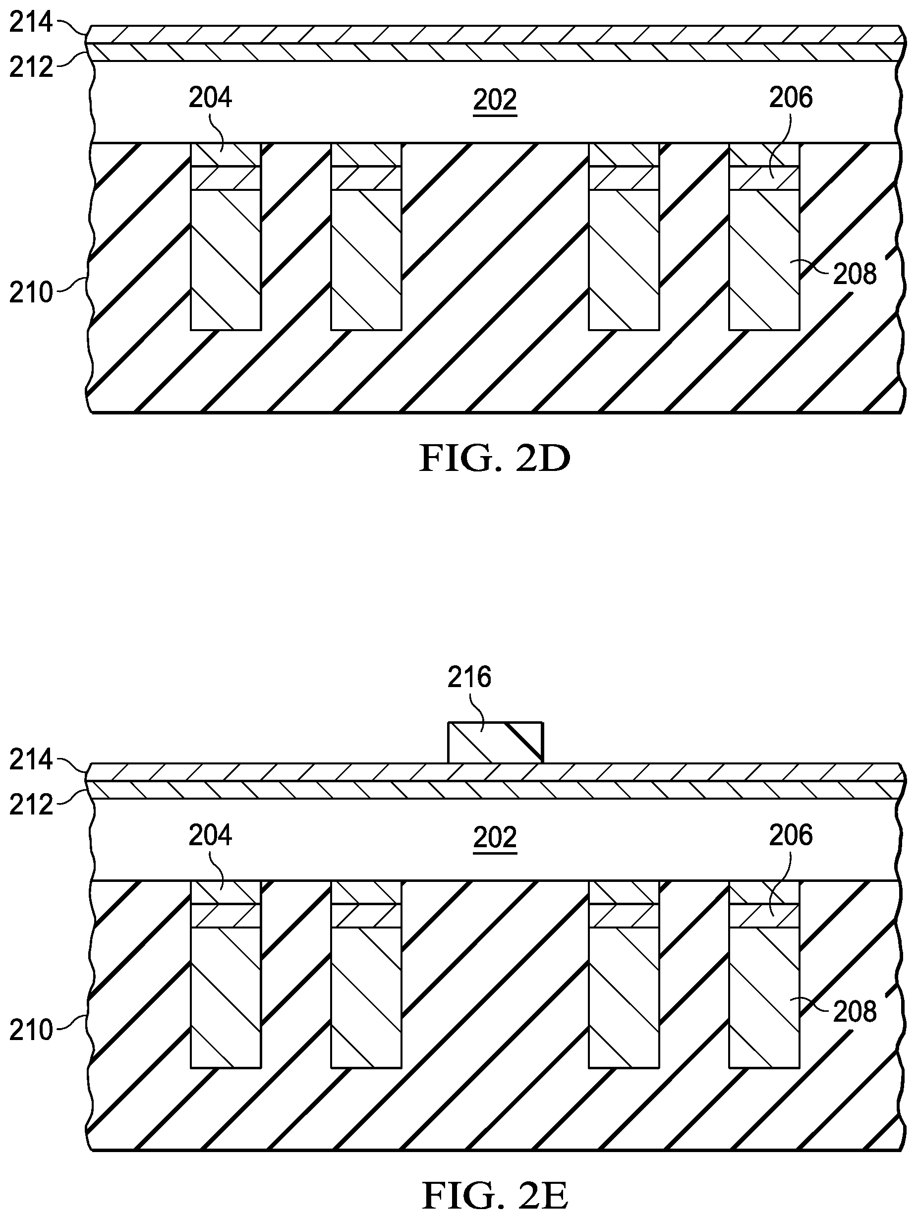
FIG. 1 is a process flow diagram of an example process 100 illustrated in FIGS. 2A-K. Step 102 is providing a semiconductor wafer 202 (FIG. 2A) having active components (not shown) and contacts, as shown in FIG. 2A as pillars including titanium-tungsten layer (TiW) 204, seed copper layer 206 and plated copper layer 208. A "semiconductor wafer" is a thin, usually circular slice of semiconductor material such as silicon, gallium arsenide, silicon germanium, III-V and 11-IV compound semiconductor materials. A "seed layer" is a layer deposited to promote preferential growth of a subsequent layer. In this case, copper seed layer 206 provides the nucleation sites for formation of copper layer 208 by, for example, electroless plating. Step 104 is covering the active side of the semiconductor wafer (i.e., the side with active devices and contact pillars) with a protective polymer 210 (FIG. 2B), such as CONDOX, which is commercially available from DISCO Corporation of Japan. The "active side" of a semiconductor wafer is the side where active components such as transistors and diodes are formed.
Step 106 is thinning semiconductor wafer 202 as shown in FIG. 2C. The thinned semiconductor wafer 202 is 150.mu. thick, for example. In FIG. 2C, the assembly is inverted so that the backside is up. The "backside" is the opposite side of the semiconductor wafer from the active side. Step 108 is depositing a titanium-tungsten (TIW) layer 212 (FIG. 2D) as a diffusion barrier layer using sputtering, physical vapor deposition (PVD) or chemical vapor deposition (CVD) or another suitable deposition process to a thickness of 50 to 600 nm. A "diffusion barrier layer" is a layer to prevent intermixing of materials. In this case, TiW layer 212 prevents migration of copper into semiconductor wafer 202. Copper seed layer 214 is formed on TiW layer 212 using sputtering, physical vapor deposition (PVD) or chemical vapor deposition (CVD) or other suitable deposition process to a thickness of 50 to 600 nm.
Step 110 is forming a patterned layer such as photolithographic layer 216 (FIG. 2E) over the interstices or "streets" between dies when the semiconductor wafer is subsequently diced. A semiconductor wafer is "diced" when it is cut into singulated semiconductor devices or "dies." The singulated devices may be integrated circuits or individual active components. Step 112 is forming a conductive layer, such as copper layer 218 (FIG. 2F) on the exposed portions of copper seed layer 214 to a thickness of 50 to 600 nm. Copper layer 218 is formed using a plating process such as electroless plating or electrolytic plating.
Step 114 is removing photolithographic layer 216 as shown in FIG. 2G. Step 116 is etching copper seed layer 214 and TiW layer 212 using copper layer 218 as a mask as shown in FIG. 2H. These layers are etched chemically using appropriate etchant such as mixture of sulfuric acid and ferric chloride for etching copper seed and hydrogen peroxide for etching TiW. Step 118 is forming a silver layer 220 on copper layer 218 as shown in FIG. 2I. Silver layer 220 is formed using immersion plating to a thickness of 1.mu., for example. Immersion plating of silver uses a dissolved salt of silver, such as silver cyanides, silver nitrates and others (See, Torok, et al. "Nanoscale characterization of thin immersion silver coatings on copper substrates," Cornell University Library arXiv:1502.01579 [cond-mat.mtrl-sci] (5 Feb. 2015) (available at the uniform resource locator (URL):https://arxiv.org/abs/1502.01579), which is hereby incorporated herein by reference). In addition, the immersion solution can contain chemicals to set pH levels and organic solderability preservatives. Example organic solderability preservatives are discussed in Cole et al., U.S. Pat. No. 5,858,074 issued Jan. 12, 1999, which is hereby incorporated herein by reference. The use of organic solderability preservatives improves solder contacts to silver layer 220, as well as improving other types of connections to silver layer 220, such as silver paste. Step 120 dices the semiconductor wafer 202 into individual dies as shown in FIG. 2J. Step 122 removes the polymer 210 to provide the structure in FIG. 2K, which is ready for packaging. For example, each die may be encapsulated in an encapsulant such as mold compound except for contacts to the pillars and the surface of silver layer 220. In an example configuration, the surface of layer 220 is soldered to a contact to provide rapid thermal transmission from the die, through copper layer 218 and silver layer 220. Thus, the high thermal conductivity of copper and silver provides good thermal management without the cost of gold plating or the complications tin plating (carcinogenic immersion solution, tin whiskers, intermetallic compound formation and others).
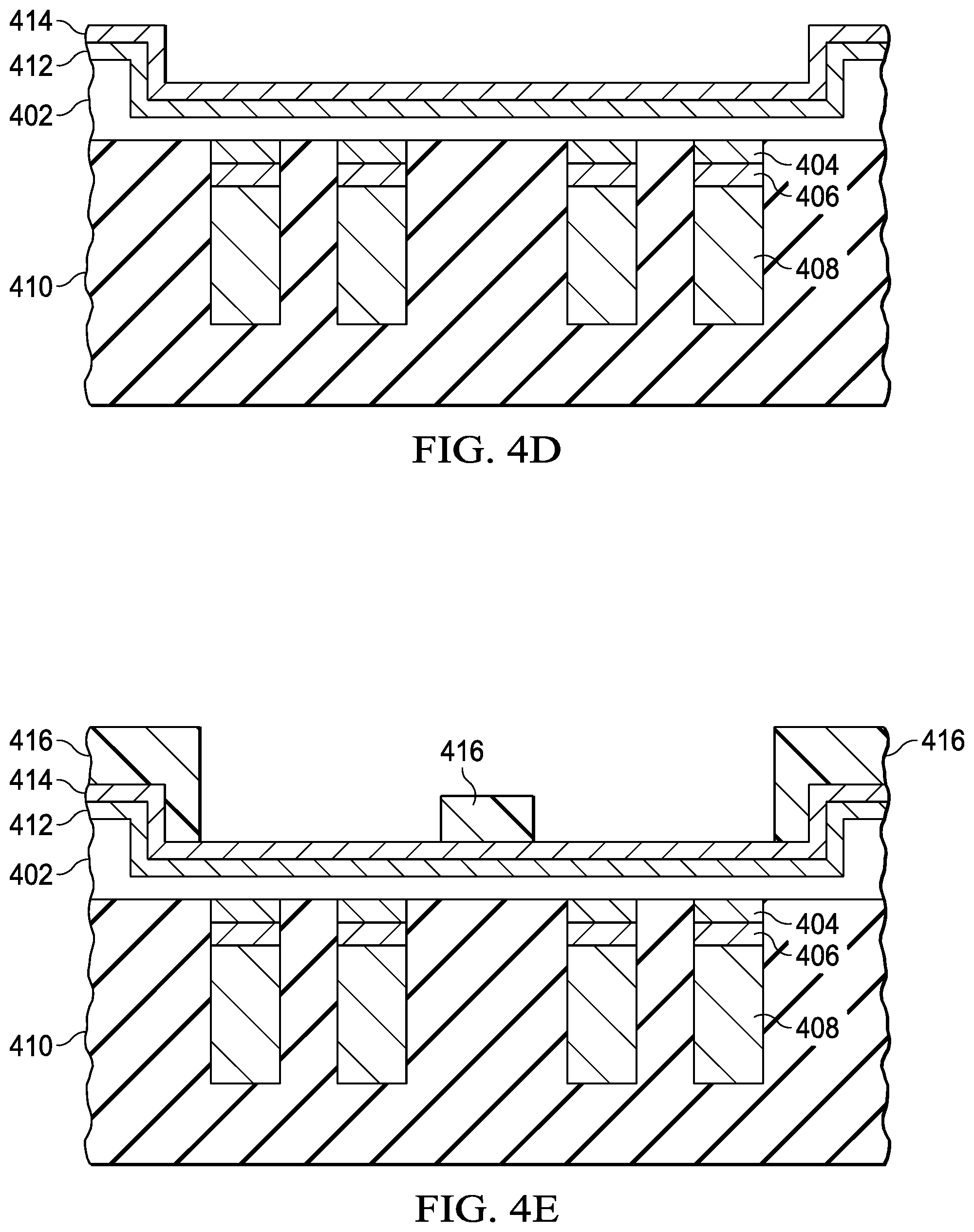
FIG. 3 is a flow diagram of an example process 300 illustrated in FIGS. 4A-K. Step 302 is forming active devices and contacts in a semiconductor wafer 402 (FIG. 4A). In this example, the contacts are pillars that include TiW layer 404, seed copper layer 406 and plated copper layer 408. Step 304 forms a layer of CONDOX 410 by, for example, a spin-on process to cover the active side of semiconductor wafer 402 (FIG. 4B). Step 306 thins the semiconductor wafer 402 (FIG. 4C) using the TAIKO process. DISCO Corporation of Japan developed the TAIKO process, which thins the semiconductor wafer except for a 3 mm rim around the periphery of the semiconductor wafer. The 3 mm rim provides stiffness to the entire semiconductor wafer to avoid problems such as die warpage.
Step 308 is depositing a diffusion barrier layer such as TiW layer 412 on the backside of semiconductor wafer 402 (FIG. 4D) using sputtering, physical vapor deposition (PVD) or chemical vapor deposition (CVD) or another suitable deposition process to a thickness of 50 to 600 nm. A seed copper layer 414 is then formed on TiW layer 412 using sputtering, physical vapor deposition (PVD) or chemical vapor deposition (CVD) or another suitable deposition process to a thickness of 50 to 600 nm. Step 310 forms a patterned layer such as photoresist layer 416 on seed copper layer 414 (FIG. 4E). The openings in photoresist layer in this example are less than the area of each die in semiconductor wafer 402. Thus, the photoresist layer covers the area between dies.
Step 312 is forming conductive layers such as copper layers 418 on the exposed portions of seed copper layer 414 (FIG. 4F) using, for example, electroless or electrolytic plating. Step 314 is forming silver layer 420 on the surface of copper layer 418 (FIG. 4G) using, for example, immersion plating with silver nitrate to a thickness of 1.mu., for example. Other salts of silver may be used in other examples. In addition, the immersion solution may include organic solderability preservatives. Step 316 is removing photoresist layer 416 as shown in FIG. 4H.
Step 318 etches seed copper layer 414 and TiW layer 412 using copper layer 418 and silver layer 420 (FIG. 4I) as an etch mask. These layers are etched chemically using appropriate etchant such as mixture of sulfuric acid and ferric chloride for etching copper seed and hydrogen peroxide for etching TiW. Step 320 is dicing semiconductor wafer 402 (FIG. 4J). As noted above, the conductive stack including TiW layer 412, seed copper layer 414, copper layer 418 and silver layer 420 are not in the regions between dies or "streets." Step 322 is removing CONDOX 410 as shown in FIG. 4K.
FIG. 5 is a flow diagram of an example process 500 illustrated in FIGS. 6A-L. Step 502 is forming active devices in a semiconductor wafer 602 (FIG. 6A). Step 504 is thinning the backside of semiconductor wafer 602 (FIG. 6B). The backside is the opposite side to the active side, i.e. the side where the active devices are formed. In this example, semiconductor wafer 602 is thinned using the TAIKO process to a thickness of 150.mu., for example. Step 506 is forming a TiW layer 604 on the active side of semiconductor wafer 602 and a TiW layer 608 on the backside of semiconductor wafer 602. TiW layers 604 and 608 may be formed separately or simultaneously using sputtering, physical vapor deposition (PVD) or chemical vapor deposition (CVD) or other suitable deposition process to a thickness of 50 to 600 nm. Seed copper layer 606 is formed on TiW layer 604 and seed copper layer 610 is formed on TiW layer 608, either simultaneously or separately, using sputtering, physical vapor deposition (PVD) or chemical vapor deposition (CVD) or another suitable deposition process to a thickness of 50 to 600 nm (FIG. 6C). Step 508 is forming photoresist layer on seed copper layer 606 and seed copper layer 610 as shown in FIG. 6D using, for example, a spin-on process.
Step 510 is patterning photoresist 612 to provide a patterned layer as shown in FIG. 6E. On the active side of semiconductor wafer 602 over seed copper layer 606, the openings in patterned photoresist correspond to contact points on the semiconductor wafer for contact to the active devices. Step 512 is forming conductive layers such as copper layers 614 and 616 on the exposed portions of seed copper layer 606 and seed copper layer 610 using sputtering, CVD, PVD or another suitable process to a thickness of 50 to 600 nm as shown in FIG. 6F. Step 514 is removing photoresist layer 612 as shown in FIG. 6G. Step 516 is removing the portions of TiW layer 604, seed copper layer 606, TiW layer 608 and seed copper layer 610 that are not covered by copper layers 614 and 616 using, for example, etching chemically using appropriate etchant such as mixture of sulfuric acid and ferric chloride for etching copper seed and hydrogen peroxide for etching TiW as shown in FIG. 6H.
Step 518 is forming a protective polymer layer 620, such as CONDOX, on the active side of semiconductor wafer 602 (FIG. 6I). Step 520 is forming silver layer 622 on copper layer 614 using immersion plating with an organic solderability preservative to a thickness of 1.mu., for example (FIG. 6J). Step 522 is removing polymer 620 (FIG. 6K). Step 524 is dicing semiconductor wafer 602 as shown in FIG. 6L.
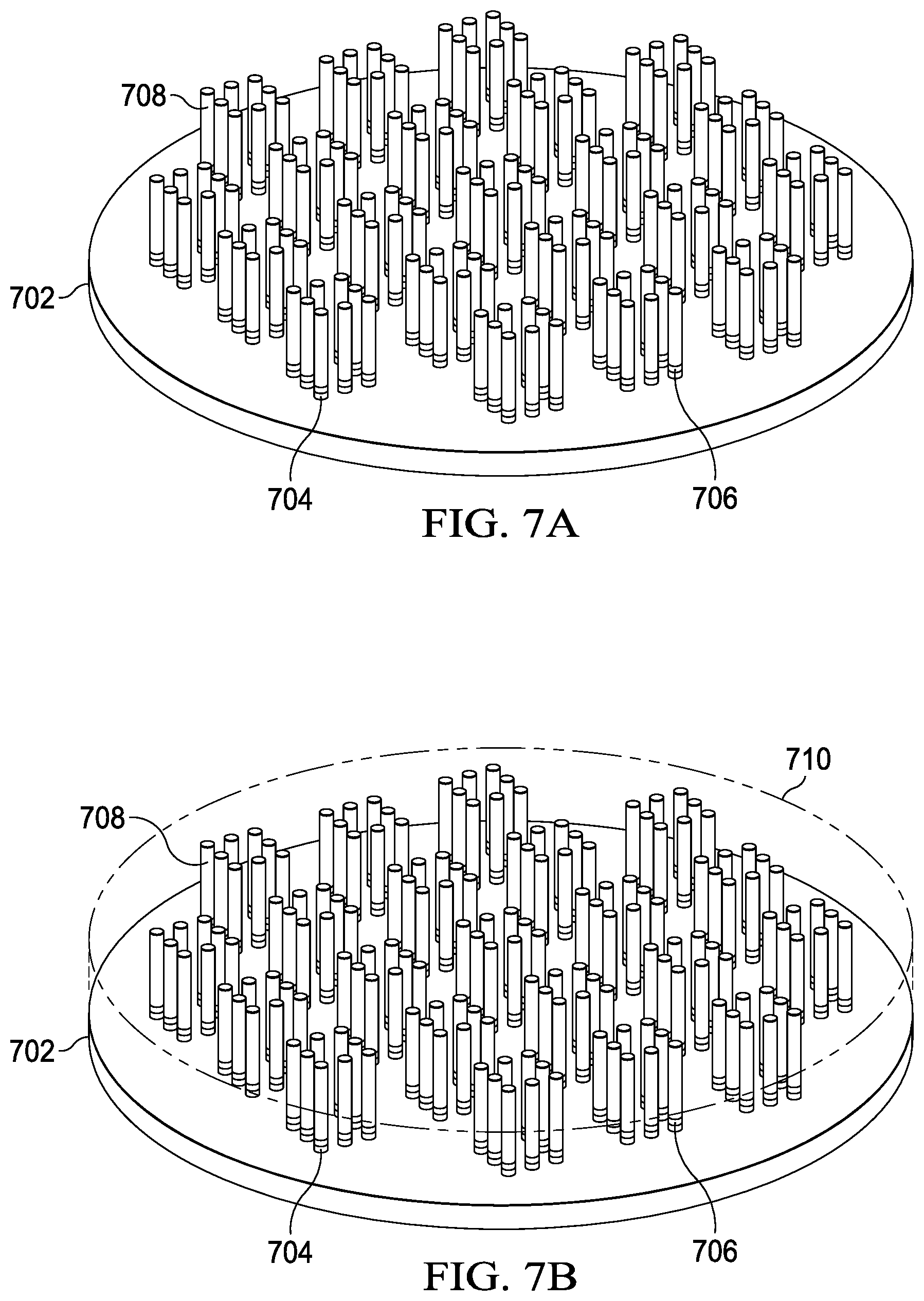
FIGS. 7A-J are perspective diagrams of an example process like process 100 (FIG. 1). FIG. 7A shows the active side of semiconductor wafer 702. Multiple copper bumps on the active side of semiconductor wafer 702 include TiW layer 704, seed copper layer 706 and copper layer 708. Each of these bumps will provide electrical contact to the active circuitry in a particular die on the semiconductor wafer. FIG. 7B shows formation of an adhesive layer 710, such as CONDOX, on the active side of semiconductor wafer 702. In FIG. 7C, semiconductor wafer 702 is inverted from the view of FIGS. 7A and B. The backside of semiconductor wafer 702 is thinned to a thickness of 150.mu. in this example. TiW layer 712 is deposited on the backside of semiconductor wafer 702 to a thickness of 50 to 600 nm, for example, using sputtering, PVD, CVD or another suitable method. FIG. 7D shows copper seed layer 714, which is deposited to a thickness of 50 to 600 nm, for example, using sputtering, PVD, CVD or another suitable method.
FIG. 7E shows photoresist layer 716, which is spun onto copper seed layer 714. As shown in FIG. 7F, photoresistor layer 716 is patterned to provide a patterned layer including an opening for each die of semiconductor wafer 702. FIG. 7G shows conductive layers such as copper layers 718, which are plated onto the exposed portions of copper seed layer 714 using electroless or electrolytic plating to a thickness of 50 to 600 nm, for example. In an additional example, silver is plated to the surface of copper layers 718 using immersion plating to a thickness of 1.mu., for example. FIG. 7H shows the resulting structure after the removal of photoresist layer 716. FIG. 7I shows the removal of the portions of copper seed layer 714 and TiW layer 712 by using chemical etchants and using copper layers 718 as an etch mask. FIG. 7J shows semiconductor wafer 702 diced into separate dies. The singulated dies are then encapsulated using an encapsulant such as mold compound, except to leave copper layers 718 and the bumps on the active side exposed. In one example, the solder balls cover the exposed portion of the bumps to provide a ball grid array.
FIG. 8 is a chemical diagram of one trimethoxysilane radical from (3-mercaptopropyl)trimethoxysilane. The sulfanyl (mercapto) radical (HS) binds the trimethoxysilane radicals to the propyl organic chain as shown in FIG. 9. When dipped in a solution including (3-mercaptopropyl)trimethoxysilane, the sulfanyl radical mediates the bonding of the trimethoxysilane radical to the surface of the metal, such as copper or silver (as shown in FIG. 9). In one example, the solution includes 97% by volume methanol and 3% by volume (3-mercaptopropyl)trimethoxysilane. The trimethoxysilane radicals provide protection to the surface of the metal and mediates binding of conductive epoxies to the metal. The use of (3-mercaptopropyl)trimethoxysilane mitigates delamination issues between the metal and the conductive epoxies and can eliminate delamination issues. Examples of chemicals that may be substituted for (3-mercaptopropyl)trimethoxysilane are (3-Mercaptopropyl)triethoxysilane, which provides triethoxysilane radicals, and (3-Mercaptopropyl)methyldimethoxysilane, which provides methyldimethoxysilane radicals.
FIGS. 10A-F show examples of semiconductor devices using a backside copper contact. FIG. 10A shows a simple mounting of a semiconductor die 1002 having contacts 1004 and backside copper 1006. Backside copper 1006 may or may not include a silver layer formed by immersion. Backside copper 1006 is mounted to copper substrate 1010 using a conductive paste such as silver paste 1008. By preparing backside copper 1006 with (3-mercaptopropyl)trimethoxysilane as described hereinabove, the bond between backside copper 1006 and silver paste 1008 is improved. Also, the use of backside copper 1006 provides good conduction of heat away from semiconductor die 1002 through backside copper 1006, silver paste 1008 and copper substrate 1010, thus enhancing transfer of heat away from semiconductor die 1002.
FIG. 10B shows another example configuration. As with the structure of FIG. 10A, semiconductor die 1002 has contacts 1004 and backside copper 1006. Backside copper 1006 may or may not include a silver layer formed by immersion. Backside copper 1006 is mounted to copper substrate 1010 using silver paste 1008. Preparing backside copper 1006 with (3-mercaptopropyl)trimethoxysilane as described hereinabove improves the bond between backside copper 1006 and silver paste 1008. Also, the use of backside copper 1006 provides good conduction of heat away from semiconductor die 1002 through backside copper 1006, silver paste 1008 and copper substrate 1010, thus enhancing transfer of heat away from semiconductor die 1002. In addition to the structure of FIG. 10A, the structure of FIG. 10B includes an active side copper substrate 1012 and encapsulation structure 1014.
FIG. 10C shows another example configuration. As with the structure of FIG. 10B, semiconductor die 1002 has contacts 1004 and backside copper 1006. In addition, the structure of FIG. 10C includes active side copper substrate 1012 Backside copper 1006 may or may not include a silver layer formed by immersion. Backside copper 1006 is mounted to copper substrate 1010 using silver paste 1008. Preparing backside copper 1006 with (3-mercaptopropyl)trimethoxysilane improves the bond between backside copper 1006 and silver paste 1008. Also, the use of backside copper 1006 provides good conduction of heat away from semiconductor die 1002 through backside copper 1006, silver paste 1008 and copper substrate 1010, thus enhancing transfer of heat away from semiconductor die 1002. In the structure of FIG. 10C, encapsulation structure 1014 is and encapsulant such as mold compound. As shown in FIG. 10D, using patterned etching, openings 1016 are formed in copper substrate 1010 and active side copper substrate 1012. As shown in FIG. 10E, openings 1016 are used as a mask to etch encapsulation structure 1014 and silver paste 1008 to expose contacts 1004 and backside copper 1006. In FIG. 10F, a suitable deposition technique like sputtering forms copper layers 1018 and 1020 on the active side and back side, respectively. Copper layers 1018 and 1020 are then patterned to provide appropriate connections to contacts 1004 and backside copper 1006.
Modifications are possible in the described examples, and other examples are possible, within the scope of the claims.
* * * * *
References
D00000
D00001
D00002
D00003
D00004
D00005
D00006
D00007
D00008
D00009
D00010
D00011
D00012

D00013

D00014

D00015

D00016

D00017

D00018
D00019

D00020

D00021

D00022

D00023

D00024

D00025

D00026

XML
uspto.report is an independent third-party trademark research tool that is not affiliated, endorsed, or sponsored by the United States Patent and Trademark Office (USPTO) or any other governmental organization. The information provided by uspto.report is based on publicly available data at the time of writing and is intended for informational purposes only.
While we strive to provide accurate and up-to-date information, we do not guarantee the accuracy, completeness, reliability, or suitability of the information displayed on this site. The use of this site is at your own risk. Any reliance you place on such information is therefore strictly at your own risk.
All official trademark data, including owner information, should be verified by visiting the official USPTO website at www.uspto.gov. This site is not intended to replace professional legal advice and should not be used as a substitute for consulting with a legal professional who is knowledgeable about trademark law.