Word line decoder memory architecture
Berger , et al.
U.S. patent number 10,699,761 [Application Number 16/134,869] was granted by the patent office on 2020-06-30 for word line decoder memory architecture. This patent grant is currently assigned to Spin Memory, Inc.. The grantee listed for this patent is SPIN MEMORY, Inc.. Invention is credited to Neal Berger, Susmita Karmakar, Benjamin Louie.


| United States Patent | 10,699,761 |
| Berger , et al. | June 30, 2020 |
Word line decoder memory architecture
Abstract
A clocked driver circuit can include a level shifter latch and a driver. The level shifter latch can be configured to receive an input signal upon a clock signal and generate a level shifted output signal. The driver can be configured to receive the level shifted output signal from the level shifter and drive the output signal on a line. The signal levels of the output signal can be greater than the signal level of the input signal.
| Inventors: | Berger; Neal (Cupertino, CA), Karmakar; Susmita (Fremont, CA), Louie; Benjamin (Fremont, CA) | ||||||||||
|---|---|---|---|---|---|---|---|---|---|---|---|
| Applicant: |
|
||||||||||
| Assignee: | Spin Memory, Inc. (Fremont,
CA) |
||||||||||
| Family ID: | 69774310 | ||||||||||
| Appl. No.: | 16/134,869 | ||||||||||
| Filed: | September 18, 2018 |
Prior Publication Data
| Document Identifier | Publication Date | |
|---|---|---|
| US 20200090721 A1 | Mar 19, 2020 | |
| Current U.S. Class: | 1/1 |
| Current CPC Class: | G11C 8/10 (20130101); G11C 13/0028 (20130101); G11C 5/14 (20130101); G11C 5/147 (20130101); G11C 11/1657 (20130101); G11C 11/1659 (20130101); G11C 8/08 (20130101) |
| Current International Class: | G11C 8/08 (20060101); G11C 11/16 (20060101); G11C 8/10 (20060101); G11C 5/14 (20060101) |
References Cited [Referenced By]
U.S. Patent Documents
| 4597487 | July 1986 | Crosby et al. |
| 5541868 | July 1996 | Prinz |
| 5559952 | September 1996 | Fujimoto |
| 5629549 | May 1997 | Johnson |
| 5640343 | June 1997 | Gallagher et al. |
| 5654566 | August 1997 | Johnson |
| 5691936 | November 1997 | Sakahima et al. |
| 5695846 | December 1997 | Lange et al. |
| 5695864 | December 1997 | Zlonczweski |
| 5732016 | March 1998 | Chen et al. |
| 5751647 | May 1998 | O'Toole |
| 5856897 | January 1999 | Mauri |
| 5896252 | April 1999 | Kanai |
| 5966323 | October 1999 | Chen et al. |
| 6016269 | January 2000 | Peterson et al. |
| 6055179 | April 2000 | Koganei et al. |
| 6064948 | May 2000 | West |
| 6075941 | June 2000 | Itoh |
| 6097579 | August 2000 | Gill |
| 6112295 | August 2000 | Bhamidipati et al. |
| 6124711 | September 2000 | Tanaka et al. |
| 6134138 | October 2000 | Lu et al. |
| 6140838 | October 2000 | Johnson |
| 6154139 | November 2000 | Kanai et al. |
| 6154349 | November 2000 | Kanai et al. |
| 6172902 | January 2001 | Wegrowe et al. |
| 6233172 | May 2001 | Chen et al. |
| 6233690 | May 2001 | Choi et al. |
| 6243288 | June 2001 | Ishikawa et al. |
| 6252798 | June 2001 | Satoh et al. |
| 6256223 | July 2001 | Sun |
| 6292389 | September 2001 | Chen et al. |
| 6347049 | February 2002 | Childress et al. |
| 6376260 | April 2002 | Chen et al. |
| 6385082 | May 2002 | Abraham et al. |
| 6436526 | August 2002 | Odagawa et al. |
| 6442681 | August 2002 | Ryan et al. |
| 6458603 | October 2002 | Kersch et al. |
| 6493197 | December 2002 | Ito et al. |
| 6522137 | February 2003 | Sun et al. |
| 6532164 | March 2003 | Radon et al. |
| 6538918 | March 2003 | Swanson et al. |
| 6545903 | April 2003 | Savtchenko et al. |
| 6545906 | April 2003 | Savtchenko et al. |
| 6563681 | May 2003 | Sasaki et al. |
| 6566246 | May 2003 | deFelipe et al. |
| 6603677 | August 2003 | Redon et al. |
| 6653153 | November 2003 | Doan et al. |
| 6654278 | November 2003 | Engel et al. |
| 6677165 | January 2004 | Lu et al. |
| 6710984 | March 2004 | Yuasa et al. |
| 6713195 | March 2004 | Wang et al. |
| 6714444 | March 2004 | Huai et al. |
| 6731537 | May 2004 | Kanamori |
| 6744086 | June 2004 | Daughton et al. |
| 6750491 | June 2004 | Sharma et al. |
| 6765824 | July 2004 | Kishi et al. |
| 6772036 | August 2004 | Eryurek et al. |
| 6773515 | August 2004 | Li et al. |
| 6777730 | August 2004 | Daughton et al. |
| 6785159 | August 2004 | Tuttle |
| 6812437 | November 2004 | Levy |
| 6829161 | December 2004 | Huai et al. |
| 6835423 | December 2004 | Chen et al. |
| 6838740 | January 2005 | Huai et al. |
| 6839821 | January 2005 | Estakhri |
| 6842317 | January 2005 | Sugita et al. |
| 6847547 | January 2005 | Albert et al. |
| 6887719 | May 2005 | Lu et al. |
| 6888742 | May 2005 | Nguyen et al. |
| 6902807 | June 2005 | Argitia et al. |
| 6906369 | June 2005 | Ross et al. |
| 6920063 | July 2005 | Huai et al. |
| 6933155 | August 2005 | Albert et al. |
| 6938142 | August 2005 | Pawlowski |
| 6958927 | October 2005 | Nguyen et al. |
| 6967863 | November 2005 | Huai |
| 6980469 | December 2005 | Kent et al. |
| 6985385 | January 2006 | Nguyen et al. |
| 6992359 | January 2006 | Nguyen et al. |
| 6995962 | February 2006 | Saito et al. |
| 7002839 | February 2006 | Kawabata et al. |
| 7005958 | February 2006 | Wan |
| 7006371 | February 2006 | Matsuoka |
| 7006375 | February 2006 | Covington |
| 7009877 | March 2006 | Huai et al. |
| 7041598 | May 2006 | Sharma |
| 7045368 | May 2006 | Hong et al. |
| 7057922 | June 2006 | Fukumoto |
| 7170778 | January 2007 | Kent et al. |
| 7187577 | March 2007 | Wang |
| 7190611 | March 2007 | Nguyen et al. |
| 7203129 | April 2007 | Lin et al. |
| 7227773 | June 2007 | Nguyen et al. |
| 7262941 | August 2007 | Li et al. |
| 7307876 | December 2007 | Kent et al. |
| 7324387 | January 2008 | Bergemont et al. |
| 7335960 | February 2008 | Han et al. |
| 7351594 | April 2008 | Bae et al. |
| 7352021 | April 2008 | Bae et al. |
| 7372722 | May 2008 | Jeong |
| 7376006 | May 2008 | Bednorz et al. |
| 7386765 | June 2008 | Ellis |
| 7436699 | October 2008 | Tanizaki |
| 7443223 | October 2008 | Bajkowski |
| 7449345 | November 2008 | Horng et al. |
| 7453719 | November 2008 | Sakimura |
| 7476919 | January 2009 | Hong et al. |
| 7502249 | March 2009 | Ding |
| 7573737 | August 2009 | Kent et al. |
| 7598555 | October 2009 | Papworth-Parkin |
| 7619431 | November 2009 | DeWilde et al. |
| 7642612 | January 2010 | Izumi et al. |
| 7660161 | February 2010 | Van Tran |
| 7733699 | June 2010 | Roohparvar |
| 7773439 | August 2010 | Do et al. |
| 7776665 | August 2010 | Izumi et al. |
| 7800407 | September 2010 | Agarwal |
| 7852662 | December 2010 | Yang |
| 7881095 | February 2011 | Lu |
| 7911832 | March 2011 | Kent et al. |
| 7936595 | May 2011 | Han et al. |
| 7986544 | July 2011 | Kent et al. |
| 8080365 | December 2011 | Nozaki |
| 8088556 | January 2012 | Nozaki |
| 8094480 | January 2012 | Tonomura |
| 8144509 | March 2012 | Jung |
| 8148970 | April 2012 | Fuse |
| 8164971 | April 2012 | Wang |
| 8255742 | August 2012 | Ipek |
| 8278996 | October 2012 | Miki |
| 8279666 | October 2012 | Dieny et al. |
| 8334213 | December 2012 | Mao |
| 8349536 | January 2013 | Nozaki |
| 8363465 | January 2013 | Kent et al. |
| 8386836 | February 2013 | Burger |
| 8432727 | April 2013 | Ryu |
| 8441844 | May 2013 | El Baraji |
| 8456883 | June 2013 | Liu |
| 8456926 | June 2013 | Ong |
| 8492881 | July 2013 | Kuroiwa et al. |
| 8535952 | September 2013 | Ranjan et al. |
| 8539303 | September 2013 | Lu |
| 8549303 | October 2013 | Fifield et al. |
| 8574928 | November 2013 | Satoh et al. |
| 8582353 | November 2013 | Lee |
| 8593868 | November 2013 | Park |
| 8617408 | December 2013 | Balamane |
| 8625339 | January 2014 | Ong |
| 8634232 | January 2014 | Oh |
| 8716817 | May 2014 | Saida |
| 8737137 | May 2014 | Choy et al. |
| 8780617 | July 2014 | Kang |
| 8792269 | July 2014 | Abedifard |
| 8824237 | September 2014 | Wang |
| 8852760 | October 2014 | Wang et al. |
| 8902628 | December 2014 | Ha |
| 8966345 | February 2015 | Wilkerson |
| 9019754 | April 2015 | Bedeschi |
| 9026888 | May 2015 | Kwok |
| 9043674 | May 2015 | Wu |
| 9082888 | July 2015 | Kent et al. |
| 9104595 | August 2015 | Sah |
| 9140747 | September 2015 | Kim |
| 9165629 | October 2015 | Chih |
| 9166155 | October 2015 | Deshpande |
| 9229853 | January 2016 | Khan |
| 9245608 | January 2016 | Chen et al. |
| 9250990 | February 2016 | Motwani |
| 9263667 | February 2016 | Pinarbasi |
| 9298552 | March 2016 | Leem |
| 9299412 | March 2016 | Naeimi |
| 9317429 | April 2016 | Ramanujan |
| 9337412 | May 2016 | Pinarbasi et al. |
| 9362486 | June 2016 | Kim et al. |
| 9378317 | June 2016 | Kawai |
| 9396991 | July 2016 | Arvin et al. |
| 9401336 | July 2016 | Arvin et al. |
| 9406876 | August 2016 | Pinarbasi |
| 9418721 | August 2016 | Bose |
| 9449720 | September 2016 | Lung |
| 9450180 | September 2016 | Annunziata |
| 9455013 | September 2016 | Kim |
| 9472282 | October 2016 | Lee |
| 9472748 | October 2016 | Kuo et al. |
| 9484527 | November 2016 | Han et al. |
| 9488416 | November 2016 | Fujita et al. |
| 9508456 | November 2016 | Shim |
| 9548445 | January 2017 | Lee et al. |
| 9553102 | January 2017 | Wang |
| 9583167 | February 2017 | Chung |
| 9728712 | August 2017 | Kardasz et al. |
| 9741926 | August 2017 | Pinarbasi et al. |
| 9772555 | September 2017 | Park et al. |
| 9773974 | September 2017 | Pinarbasi et al. |
| 9853006 | December 2017 | Arvin et al. |
| 9853206 | December 2017 | Pinarbasi et al. |
| 9853292 | December 2017 | Loveridge et al. |
| 9865806 | January 2018 | Choi et al. |
| 10026609 | July 2018 | Sreenivasan et al. |
| 10043851 | August 2018 | Shen |
| 10115446 | October 2018 | Louie et al. |
| 10163479 | December 2018 | Yoha |
| 2002/0057593 | May 2002 | Hidaka |
| 2002/0090533 | July 2002 | Zhang et al. |
| 2002/0105823 | August 2002 | Redon et al. |
| 2002/0132140 | September 2002 | Igarashi et al. |
| 2003/0085186 | May 2003 | Fujioka |
| 2003/0117840 | June 2003 | Sharma et al. |
| 2003/0151944 | August 2003 | Saito |
| 2003/0197984 | October 2003 | Inomata et al. |
| 2003/0218903 | November 2003 | Luo |
| 2004/0012994 | January 2004 | Slaughter et al. |
| 2004/0026369 | February 2004 | Ying |
| 2004/0047179 | March 2004 | Chan |
| 2004/0061154 | April 2004 | Huai et al. |
| 2004/0094785 | May 2004 | Zhu et al. |
| 2004/0130936 | July 2004 | Nguyen et al. |
| 2004/0173315 | September 2004 | Leung |
| 2004/0197174 | October 2004 | Van Den Berg |
| 2004/0221030 | November 2004 | Huras |
| 2004/0257717 | December 2004 | Sharma et al. |
| 2005/0022746 | February 2005 | Lampe |
| 2005/0029551 | February 2005 | Atwood et al. |
| 2005/0041342 | February 2005 | Huai et al. |
| 2005/0051820 | March 2005 | Stojakovic et al. |
| 2005/0063222 | March 2005 | Huai et al. |
| 2005/0104101 | May 2005 | Sun et al. |
| 2005/0128842 | June 2005 | Wei |
| 2005/0136600 | June 2005 | Huai |
| 2005/0158881 | July 2005 | Sharma |
| 2005/0160205 | July 2005 | Kuo |
| 2005/0174702 | August 2005 | Gill |
| 2005/0180202 | August 2005 | Huai et al. |
| 2005/0184839 | August 2005 | Nguyen et al. |
| 2005/0201023 | September 2005 | Huai et al. |
| 2005/0237787 | October 2005 | Huai et al. |
| 2005/0251628 | November 2005 | Jarvis et al. |
| 2005/0280058 | December 2005 | Pakala et al. |
| 2005/0285176 | December 2005 | Kim |
| 2006/0018057 | January 2006 | Huai |
| 2006/0049472 | March 2006 | Diao et al. |
| 2006/0077734 | April 2006 | Fong |
| 2006/0087880 | April 2006 | Mancoff et al. |
| 2006/0092696 | May 2006 | Bessho |
| 2006/0132990 | June 2006 | Morise et al. |
| 2006/0198202 | September 2006 | Erez |
| 2006/0227465 | October 2006 | Inokuchi et al. |
| 2006/0271755 | November 2006 | Miura |
| 2006/0284183 | December 2006 | Izumi et al. |
| 2006/0291305 | December 2006 | Suzuki et al. |
| 2007/0019337 | January 2007 | Apalkov et al. |
| 2007/0094573 | April 2007 | Chen |
| 2007/0096229 | May 2007 | Yoshikawa |
| 2007/0220935 | September 2007 | Cernea |
| 2007/0226592 | September 2007 | Radke |
| 2007/0242501 | October 2007 | Hung et al. |
| 2007/0283313 | December 2007 | Ogawa |
| 2007/0285972 | December 2007 | Horii |
| 2008/0049487 | February 2008 | Yoshimura |
| 2008/0049488 | February 2008 | Rizzo |
| 2008/0079530 | April 2008 | Weidman et al. |
| 2008/0112094 | May 2008 | Kent et al. |
| 2008/0144376 | June 2008 | Lee |
| 2008/0151614 | June 2008 | Guo |
| 2008/0181009 | July 2008 | Arai |
| 2008/0259508 | October 2008 | Kent et al. |
| 2008/0294938 | November 2008 | Kondo |
| 2008/0297292 | December 2008 | Viala et al. |
| 2009/0040825 | February 2009 | Adusumilli et al. |
| 2009/0046501 | February 2009 | Ranjan et al. |
| 2009/0072185 | March 2009 | Raksha et al. |
| 2009/0078927 | March 2009 | Mao |
| 2009/0080267 | March 2009 | Bedeschi |
| 2009/0091037 | April 2009 | Assefa et al. |
| 2009/0098413 | April 2009 | Kanegae |
| 2009/0130779 | May 2009 | Li |
| 2009/0146231 | June 2009 | Kuper et al. |
| 2009/0161421 | June 2009 | Cho et al. |
| 2009/0209102 | August 2009 | Zhong et al. |
| 2009/0231909 | September 2009 | Dieny et al. |
| 2010/0039136 | February 2010 | Chua-Eoan |
| 2010/0080040 | April 2010 | Choi |
| 2010/0087048 | April 2010 | Izumi et al. |
| 2010/0110803 | May 2010 | Arai |
| 2010/0124091 | May 2010 | Cowburn |
| 2010/0162065 | June 2010 | Norman |
| 2010/0193891 | August 2010 | Wang et al. |
| 2010/0195362 | August 2010 | Norman |
| 2010/0195401 | August 2010 | Jeong et al. |
| 2010/0227275 | September 2010 | Nozaki |
| 2010/0232206 | September 2010 | Li |
| 2010/0246254 | September 2010 | Prejbeanu et al. |
| 2010/0248154 | September 2010 | Nozaki |
| 2010/0254181 | October 2010 | Chung |
| 2010/0271090 | October 2010 | Rasmussen |
| 2010/0271870 | October 2010 | Zheng et al. |
| 2010/0277976 | November 2010 | Oh |
| 2010/0290275 | November 2010 | Park |
| 2010/0311243 | December 2010 | Mao |
| 2011/0001108 | January 2011 | Greene |
| 2011/0032645 | February 2011 | Noel et al. |
| 2011/0058412 | March 2011 | Zheng et al. |
| 2011/0061786 | March 2011 | Mason |
| 2011/0076620 | March 2011 | Nozaki |
| 2011/0089511 | April 2011 | Keshtbod et al. |
| 2011/0133298 | June 2011 | Chen et al. |
| 2011/0283135 | November 2011 | Burger |
| 2011/0310691 | December 2011 | Zhou et al. |
| 2011/0320596 | December 2011 | Fee et al. |
| 2012/0028373 | February 2012 | Belen |
| 2012/0052258 | March 2012 | Op DeBeeck et al. |
| 2012/0069649 | March 2012 | Ranjan et al. |
| 2012/0127804 | May 2012 | Ong et al. |
| 2012/0155158 | June 2012 | Higo |
| 2012/0163113 | June 2012 | Hatano et al. |
| 2012/0280336 | June 2012 | Watts |
| 2012/0181642 | July 2012 | Prejbeanu et al. |
| 2012/0188818 | July 2012 | Ranjan et al. |
| 2012/0221905 | August 2012 | Burger |
| 2012/0228728 | September 2012 | Ueki et al. |
| 2012/0239969 | September 2012 | Dickens |
| 2012/0254636 | October 2012 | Tsukamoto et al. |
| 2012/0280339 | November 2012 | Zhang et al. |
| 2012/0294078 | November 2012 | Kent et al. |
| 2012/0299133 | November 2012 | Son et al. |
| 2012/0324274 | December 2012 | Hori |
| 2013/0001506 | January 2013 | Sato et al. |
| 2013/0001652 | January 2013 | Yoshikawa et al. |
| 2013/0021841 | January 2013 | Zhou et al. |
| 2013/0039119 | February 2013 | Rao |
| 2013/0044537 | February 2013 | Ishigaki |
| 2013/0075845 | March 2013 | Chen et al. |
| 2013/0107633 | May 2013 | Kim |
| 2013/0244344 | September 2013 | Malmhall |
| 2013/0267042 | October 2013 | Satoh et al. |
| 2013/0270523 | October 2013 | Wang et al. |
| 2013/0270661 | October 2013 | Yi et al. |
| 2013/0275691 | October 2013 | Chew |
| 2013/0307097 | November 2013 | Yi et al. |
| 2013/0341801 | December 2013 | Satoh et al. |
| 2014/0009994 | January 2014 | Parkin et al. |
| 2014/0036573 | February 2014 | Ishihara |
| 2014/0042571 | February 2014 | Gan et al. |
| 2014/0048896 | February 2014 | Huang et al. |
| 2014/0063949 | March 2014 | Tokiwa |
| 2014/0070341 | March 2014 | Beach et al. |
| 2014/0089762 | March 2014 | Pangal et al. |
| 2014/0103469 | April 2014 | Jan |
| 2014/0103472 | April 2014 | Kent et al. |
| 2014/0136870 | May 2014 | Breternitz et al. |
| 2014/0149827 | May 2014 | Kim et al. |
| 2014/0151837 | June 2014 | Ryu |
| 2014/0169085 | June 2014 | Wang et al. |
| 2014/0177316 | June 2014 | Otsuka et al. |
| 2014/0217531 | August 2014 | Jan |
| 2014/0219034 | August 2014 | Gomez et al. |
| 2014/0252439 | September 2014 | Guo |
| 2014/0264671 | September 2014 | Chepulskyy et al. |
| 2014/0269005 | September 2014 | Kang |
| 2014/0281284 | September 2014 | Block et al. |
| 2014/0289358 | September 2014 | Lindamood |
| 2014/0321196 | October 2014 | Ikeda |
| 2015/0056368 | February 2015 | Wang et al. |
| 2015/0098287 | April 2015 | Lee |
| 2015/0100848 | April 2015 | Kalamatianos |
| 2015/0135039 | May 2015 | Mekhanik et al. |
| 2015/0143343 | May 2015 | Weiss |
| 2015/0154116 | June 2015 | Dittrich |
| 2015/0171316 | June 2015 | Park et al. |
| 2015/0206568 | July 2015 | Bose et al. |
| 2015/0206569 | July 2015 | Bose et al. |
| 2015/0242269 | August 2015 | Pelley et al. |
| 2015/0262701 | September 2015 | Takizawa |
| 2015/0278011 | October 2015 | Keppel et al. |
| 2015/0279904 | October 2015 | Pinarbasi et al. |
| 2015/0378814 | December 2015 | Webb et al. |
| 2015/0380088 | December 2015 | Naeimi et al. |
| 2016/0027525 | January 2016 | Kim et al. |
| 2016/0027999 | January 2016 | Pinarbasi |
| 2016/0043304 | February 2016 | Chen |
| 2016/0056072 | February 2016 | Arvin et al. |
| 2016/0085443 | March 2016 | Tomishima et al. |
| 2016/0085621 | March 2016 | Motwani |
| 2016/0085692 | March 2016 | Kwok |
| 2016/0086600 | March 2016 | Bauer et al. |
| 2016/0087193 | March 2016 | Pinarbasi et al. |
| 2016/0093798 | March 2016 | Kim et al. |
| 2016/0111634 | April 2016 | Lee et al. |
| 2016/0118249 | April 2016 | Sreenivasan et al. |
| 2016/0124299 | May 2016 | Yu et al. |
| 2016/0126201 | May 2016 | Arvin et al. |
| 2016/0126452 | May 2016 | Kuo et al. |
| 2016/0126453 | May 2016 | Chen et al. |
| 2016/0148685 | May 2016 | Roy |
| 2016/0163965 | June 2016 | Han et al. |
| 2016/0163973 | June 2016 | Pinarbasi |
| 2016/0181508 | June 2016 | Lee et al. |
| 2016/0218278 | July 2016 | Pinarbasi et al. |
| 2016/0260486 | September 2016 | Tani |
| 2016/0268499 | September 2016 | You |
| 2016/0283385 | September 2016 | Boyd et al. |
| 2016/0284762 | September 2016 | Wang et al. |
| 2016/0300615 | October 2016 | Lee |
| 2016/0307860 | October 2016 | Arvin et al. |
| 2016/0315118 | October 2016 | Kardasz et al. |
| 2016/0315249 | October 2016 | Kardasz et al. |
| 2016/0315259 | October 2016 | Fennimore et al. |
| 2016/0358778 | December 2016 | Park et al. |
| 2016/0372656 | December 2016 | Pinarbasi et al. |
| 2016/0378592 | December 2016 | Ikegami et al. |
| 2017/0025472 | January 2017 | Kim et al. |
| 2017/0033156 | February 2017 | Gan et al. |
| 2017/0033283 | February 2017 | Pinarbasi et al. |
| 2017/0047107 | February 2017 | Berger et al. |
| 2017/0062712 | March 2017 | Choi et al. |
| 2017/0069837 | March 2017 | Choi et al. |
| 2017/0084826 | March 2017 | Zhou et al. |
| 2017/0123991 | May 2017 | Sela et al. |
| 2017/0133104 | May 2017 | Darbari et al. |
| 2017/0199459 | July 2017 | Ryu et al. |
| 2017/0222132 | August 2017 | Pinarbasi et al. |
| 2017/0270988 | September 2017 | Ikegami |
| 2018/0018134 | January 2018 | Kang |
| 2018/0019343 | January 2018 | Asami |
| 2018/0033957 | February 2018 | Zhang |
| 2018/0097175 | April 2018 | Chuang |
| 2018/0114589 | April 2018 | El-Baraji et al. |
| 2018/0119278 | May 2018 | Kornmeyer |
| 2018/0121117 | May 2018 | Berger et al. |
| 2018/0121355 | May 2018 | Berger et al. |
| 2018/0121361 | May 2018 | Berger et al. |
| 2018/0122446 | May 2018 | Berger et al. |
| 2018/0122447 | May 2018 | Berger et al. |
| 2018/0122448 | May 2018 | Berger et al. |
| 2018/0122449 | May 2018 | Berger et al. |
| 2018/0122450 | May 2018 | Berger et al. |
| 2018/0130945 | May 2018 | Choi et al. |
| 2018/0211821 | July 2018 | Kogler |
| 2018/0233362 | August 2018 | Glodde |
| 2018/0233363 | August 2018 | Glodde |
| 2018/0248110 | August 2018 | Kardasz et al. |
| 2018/0248113 | August 2018 | Pinarbasi et al. |
| 2018/0331279 | November 2018 | Shen |
| 2766141 | Jan 2011 | CA | |||
| 105706259 | Jun 2016 | CN | |||
| 1345277 | Sep 2003 | EP | |||
| 2817998 | Jun 2002 | FR | |||
| 2832542 | May 2003 | FR | |||
| 2910716 | Jun 2008 | FR | |||
| H10-004012 | Jan 1998 | JP | |||
| H11-120758 | Apr 1999 | JP | |||
| H11-352867 | Dec 1999 | JP | |||
| 2001-195878 | Jul 2001 | JP | |||
| 2002-261352 | Sep 2002 | JP | |||
| 2002-357489 | Dec 2002 | JP | |||
| 2003-318461 | Nov 2003 | JP | |||
| 2005-044848 | Feb 2005 | JP | |||
| 2005-150482 | Jun 2005 | JP | |||
| 2005-535111 | Nov 2005 | JP | |||
| 2006128579 | May 2006 | JP | |||
| 2008-524830 | Jul 2008 | JP | |||
| 2009-027177 | Feb 2009 | JP | |||
| 2013-012546 | Jan 2013 | JP | |||
| 2014-039061 | Feb 2014 | JP | |||
| 5635666 | Dec 2014 | JP | |||
| 2015-002352 | Jan 2015 | JP | |||
| 10-2014-015246 | Sep 2014 | KR | |||
| 2009-080636 | Jul 2009 | WO | |||
| 2011-005484 | Jan 2011 | WO | |||
| 2014-062681 | Apr 2014 | WO | |||
Other References
|
US 7,026,672 B2, 04/2006, Grandis (withdrawn) cited by applicant . US 2016/0218273 A1, 06/2016, Pinarbasi (withdrawn) cited by applicant . Bhatti Sarpreet et al., "Spintronics Based Random Access Memory: a Review," Material Today, Nov. 2107, pp. 530-548, vol. 20, No. 9, Elsevier,. cited by applicant . Helia Naeimi, et al., "STTRAM Scaling and Retention Failure," Intel Technology Journal, vol. 17, Issue 1, 2013, pp. 54-75 (22 pages). cited by applicant . S. Ikeda, et al., "A Perpendicular-Anisotropy CoFeB-MgO Magnetic Tunnel Junction", Nature Materials, vol. 9, Sep. 2010, pp. 721-724 (4 pages). cited by applicant . R.H. Kock, et al., "Thermally Assisted Magnetization Reversal in Submicron-Sized Magnetic Thin Films", Physical Review Letters, The American Physical Society, vol. 84, No, 23, Jun. 5, 2000, pp. 5419-5422 (4 pages). cited by applicant . K.J. Lee, et al., "Analytical Investigation of Spin-Transfer Dynamics Using a Perpendicular-to-Plane Polarizer", Applied Physics Letters, American Insitute of Physics, vol. 86, (2005), pp. 022505-1 to 022505-3 (3 pages). cited by applicant . Kirsten Martens, et al., "Thermally Induced Magnetic Switching in Thin Ferromagnetic Annuli", NSF grants PHY-0351964 (DLS), 2005, 11 pages. cited by applicant . Kristen Martens, et al., "Magnetic Reversal in Nanoscropic Ferromagnetic Rings", NSF grants PHY-0351964 (DLS) 2006, 23 pages. cited by applicant . "Magnetic Technology Spintronics, Media and Interface", Data Storage Institute, R&D Highlights, Sep. 2010, 3 pages. cited by applicant . Daniel Scott Matic, "A Magnetic Tunnel Junction Compact Model for STT-RAM and MeRAM", Master Thesis University of California, Los Angeles, 2013, pp. 43. cited by applicant. |
Primary Examiner: Nguyen; Vanthu T
Claims
What is claimed is:
1. A memory device comprising: a plurality of word lines; a level shifter latch configured to receive a plurality of decoded address signals upon a first state of a clock signal and to output a plurality of word line signals, wherein the level shifter latch includes a first inverter including an input configured to receive one of the plurality of decoded address signals; a second inverter including an input coupled to an output of the first inverter; a first transmission gate including a first terminal coupled to the output of the first inverter, and a second terminal configured to receive a short pulse clock signal, wherein the short pulse clock signal is based on a rising edge of a system clock and has a shorter pulse width then the pulse width of the system clock; a second transmission gate including a first terminal coupled to an output of the second inverter, and a second terminal configured to receive the short pulse clock signal; third inverter circuit including an input coupled to a third terminal of the first transmission gate, power terminals coupled between a high voltage source, and an output terminal configured to output a first one of the plurality of word line signals; and a fourth inverter circuit including a input coupled to a third terminal of the second transmission gate and the output of first inverter circuit, power terminals coupled between the high voltage source, and an output coupled to the input of the first inverter circuit; and a word line driver configured to receive the plurality of word line signals and drive the plurality of word line signals on corresponding ones of the plurality of word lines.
2. The memory device of claim 1, wherein, the plurality of decoded address signals include a first state and a second state; and the plurality of word line signals include a third state and a fourth state, wherein a potential difference between the third state and the fourth state is greater than a potential difference between the first state and the second state.
3. The memory device of claim 1, further comprising: an address buffer configured to receive and buffer a plurality of address signals; a word line pre-decoder configured to receive the buffered plurality of address signals and output partially decoded address signals; and a word line decoder configured to receive the partially decoded address signal and output the plurality of decoded address signals.
4. The memory device of claim 1, further comprising: an array of memory cells arranged in columns and rows, wherein sets of a first number of cells arranged along columns are coupled to corresponding ones of a plurality of bit lines and sets of a second number of cells arranged along rows are coupled to corresponding ones of the plurality of word lines.
5. The memory device of claim 4, wherein each memory cell includes a select gate and a Magnetic Tunnel Junction (MTJ) coupled in series between a corresponding one of the plurality of bit lines and a corresponding one of the plurality of source lines, and wherein a control terminal of the select gate is coupled to a corresponding one of the plurality of word lines.
6. The memory device of claim 4, wherein the array of memory cells comprise an array of Spin Torque Magnetoresistive memory cells.
7. A memory device comprising: a memory cell array including a plurality of word lines; an address buffer configured to buffer a plurality of address signals, wherein the address buffer operates from a first supply potential; an address decoder circuit configured to receive the buffered plurality of address signals and output a plurality of decoded address signals, wherein the address decoder operates from the first supply potential; a level shifter latch configured to receive the plurality of decoded address signals upon a first state of a clock signal and to output a plurality of word line signals, wherein the level shifter latched operates form a second supply potential that is greater than the first supply potential, and wherein the level shifter latch includes; a first inverter including an input configured to receive one of the plurality of decoded address signals; a second inverter including an input coupled to an output of the first inverter; a first transmission gate including a control terminal configured to receive the clock signal and an input coupled to the output of the first inverter; a second transmission gate including a control terminal configured to receive the clock signal and an input coupled to the output of the second inverter; and a latch including a third inverter cross coupled to a fourth inverter, wherein an input of the third inverter is coupled to an output of the first transmission gate and an output of the fourth inverter, wherein an input of the fourth inverter is coupled to an output of the second transmission gate and an output of the third inverter, and wherein the latch operates from a second supply potential that is greater than the first supply potential; and a word line driver configured to receive the plurality of word line signals and drive the plurality of word line signals on corresponding ones of the plurality of word lines, wherein the word line driver operates form the second supply potential.
8. The memory device of claim 7, wherein the memory cell array comprises a Magnetoresistive memory cell array.
9. The memory device of claim 7, wherein the word line driver comprises: an inverting driver including an input coupled to an output of the third inverter and an output coupled to a corresponding one of the plurality of word lines, wherein the inverting driver operates from the second supply potential.
Description
BACKGROUND
Computing systems have made significant contributions toward the advancement of modern society and are utilized in a number of applications to achieve advantageous results. Numerous devices, such as desktop personal computers (PCs), laptop PCs, tablet PCs, netbooks, smart phones, servers, and the like have facilitated increased productivity and reduced costs in communicating and analyzing data in most areas of entertainment, education, business, and science. One common aspect of computing systems is computing device readable media, commonly referred to as memory.
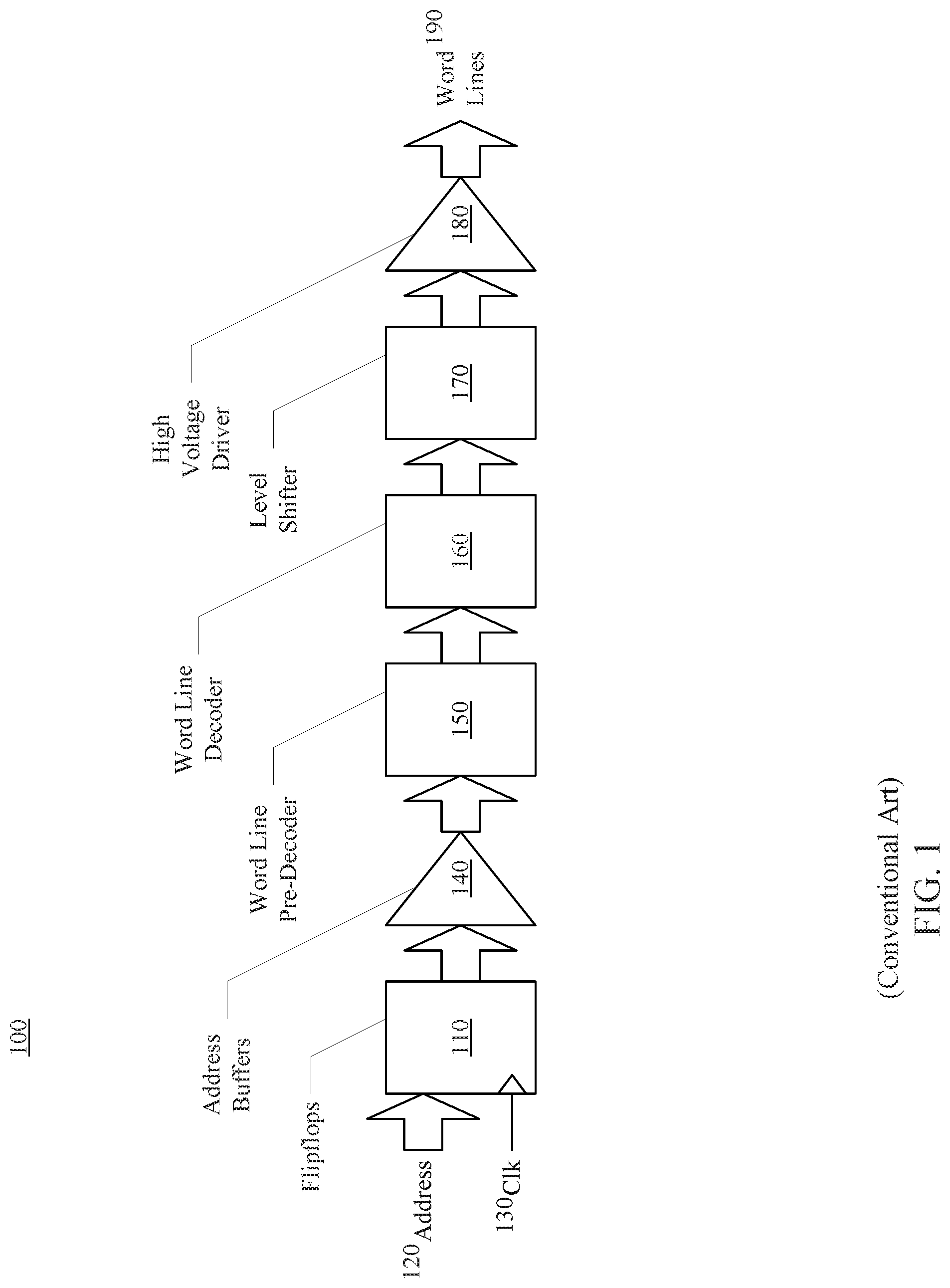
Data and instructions used by the computing system can be stored in and retrieved from one or more memory devices. When reading or writing to memory a corresponding read or write voltage potential is applied to a given word line based upon a decoded memory address. Referring to FIG. 1, a block diagram of a word line decoder and driver path architecture, according to the conventional art, is shown. The word line decoder and driver path 100 can include a plurality of flip flops 110 configured to latch a received address 120 upon receipt of a clock signal (e.g., rising or falling edge of a system clock signal) 130. A set of address buffers 140 can be configured to buffer the latched address bits from the flip flops 110. A word line pre-decoder 150 can be configured to partially decode the address in the address buffer 140. In one implementation, the word line pre-decoder 150 can be configured to decode a block, bank and/or the like portion of the memory from the address. A word line decoder 160 can be configured to decode a given word line from the partially decoded address from the word line pre-decoder 150. A level shifter 170 can be configured to shift the relatively low voltage potential signal propagating through the flip flops 110, address buffer 140, word line pre-decoder 150 and word line decoder 160 to an appropriate high voltage potential signal. A high voltage driver 180 can drive the word line 190 with the appropriate high voltage potential signal from the level shifter 170 during a read, write or erase operation. The combination of the flip flops 110, address buffers 140, word line pre-decoder 150 and word line decoder 160 can comprise an address decoder circuit, and the combination of the level shifter 170 and high voltage driver 180 can comprise a word line driver circuit.
The propagation delay through the word line decoder and driver path can be the sum of the clock-data out set up time of the flip flops 110 T.sub.C.fwdarw.Q, the propagation delay in the address buffers 140 T.sub.AB, the propagation delay through the word line pre-decoder 150 T.sub.WPD, the propagation delay through the word line decoder 160 T.sub.WD, and the propagation delay through the level shifter 170 and high voltage driver 180 T.sub.WDR. However, as computing devices continue to evolve there is a continuing need for faster memory devices. One possible way to increase the speed of the memory device is to reduce the propagation delay through the word line decoder and driver path. Therefore, there is a need for an improved word line decoder and driver path architecture.
SUMMARY
The present technology may best be understood by referring to the following description and accompanying drawings that are used to illustrate aspects of the present technology that are directed toward clocked driver circuits.
In one embodiment, a memory device can include a level shifter latch and a driver. The level shifter latch can be configured to receive a plurality of decoded address signals upon a first state of a clock signal and to output a plurality of word line signals. In one implementation, the clock signal can be a short pulse clock signal. The short pulse clock signal can be based on a rising edge of a system clock, and the pulse width of the short pulse clock signal can be shorter than the pulse width of the system clock. The decoded address signals can include a first and second state and the word line signals can include a third and fourth state, wherein a potential difference between the third and fourth states is greater than a potential difference between the first and second states. The driver can be configured to receive the plurality of word line signals and drive corresponding word lines with the plurality of word line signals.
In another embodiment, a device can include a plurality of inverters, a plurality of transmission gates, a latch and an inverting driver. A first inverter can include an input configured to receive a signal. A second inverter can include an input coupled to an output of the first inverter. The first and second inverters can operate from a first supply potential. A first transmission gate can include a control terminal configured to receive a clock signal and an input coupled to the output of the first inverter. A second transmission gate can include a control terminal configured to receive the clock signal and an input coupled to the output of the second inverter. The latch can include a third inverter cross-coupled to a fourth inverter. An input of the third inverter can be coupled to an output of the first transmission gate and an output of the fourth inverter. An input of the fourth inverter can be coupled to an output of the second transmission gate and an output of the third inverter. The inverting driver can include an input coupled to an output of the third inverter and an output configured to output a drive signal. The latch and inverting driver can operate from a second supply potential that is greater than the first supply potential.
In yet another embodiment, a memory device can include a memory cell array, an address buffer, an address decoder, a level shifter latch and a word line driver. The address buffer can be configured to buffer a plurality of address signals. The address decoder circuit can be configured to receive the buffered plurality of address signals and output a plurality of decoded address signals. The level shifter latch can be configured to receive the plurality of decoded address signals upon a first state of a clock signal and to output a plurality of word line signals. The address decoder circuit can be configured to operate from a first supply potential, while the level shifter latch can be configured to operate from a second supply potential that is greater than the first supply potential. The word line driver can be configured to receive the plurality of word line signals and drive the plurality of word line signals on word lines of the memory cell array.
This Summary is provided to introduce a selection of concepts in a simplified form that are further described below in the Detailed Description. This Summary is not intended to identify key features or essential features of the claimed subject matter, nor is it intended to be used to limit the scope of the claimed subject matter.
BRIEF DESCRIPTION OF THE DRAWINGS
Aspects of the present technology are illustrated by way of example and not by way of limitation, in the figures of the accompanying drawings and in which like reference numerals refer to similar elements and in which:
FIG. 1 shows a block diagram of a word line decoder and driver path architecture, according to the conventional art.
FIG. 2 shows a block diagram of a memory device, in accordance with aspects of the present technology.
FIG. 3 shows a block diagram of a word line decoder and driver path architecture, in accordance with aspects of the present technology.
FIG. 4 shows a timing diagram illustrating a short clock pulse utilized in the word line decoder and driver path architecture, in accordance with aspect of the present technology.
FIG. 5 shows a block diagram of a word line driver in combination with a memory cell array, in accordance with aspects of the present technology.
FIG. 6 shows a block diagram of a computing system including a memory device, in accordance with aspects of the present technology.
FIG. 7 shows a block diagram of a computing system including a memory device, in accordance with aspects of the present technology.
FIG. 8 shows a block diagram of a memory sub-system, in accordance with aspects of the present technology.
FIG. 9 shows a block diagram of a memory sub-system, in accordance with aspects of the present technology.
DETAILED DESCRIPTION
Reference will now be made in detail to the aspects of the present technology, examples of which are illustrated in the accompanying drawings. While the present technology will be described in conjunction with these aspects, it will be understood that they are not intended to limit the invention to these aspects. On the contrary, the invention is intended to cover alternatives, modifications and equivalents, which may be included within the scope of the invention as defined by the appended claims. Furthermore, in the following detailed description of the present technology, numerous specific details are set forth in order to provide a thorough understanding of the present technology. However, it is understood that the present technology may be practiced without these specific details. In other instances, well-known methods, procedures, components, and circuits have not been described in detail as not to unnecessarily obscure aspects of the present technology.
Some aspects of the present technology which follow are presented in terms of routines, modules, logic blocks, and other symbolic representations of operations on data within one or more electronic devices. The descriptions and representations are the means used by those skilled in the art to most effectively convey the substance of their work to others skilled in the art. A routine, module, logic block and/or the like, is herein, and generally, conceived to be a self-consistent sequence of processes or instructions leading to a desired result. The processes are those including physical manipulations of physical quantities. Usually, though not necessarily, these physical manipulations take the form of electric or magnetic signals capable of being stored, transferred, compared and otherwise manipulated in an electronic device. For reasons of convenience, and with reference to common usage, these signals are referred to as data, bits, values, elements, symbols, characters, terms, numbers, strings, and/or the like with reference to aspects of the present technology.
It should be borne in mind, however, that all of these terms are to be interpreted as referencing physical manipulations and quantities and are merely convenient labels and are to be interpreted further in view of terms commonly used in the art. Unless specifically stated otherwise as apparent from the following discussion, it is understood that through discussions of the present technology, discussions utilizing the terms such as "receiving," and/or the like, refer to the actions and processes of an electronic device such as an electronic computing device that manipulates and transforms data. The data is represented as physical (e.g., electronic) quantities within the electronic device's logic circuits, registers, memories and/or the like, and is transformed into other data similarly represented as physical quantities within the electronic device.
In this application, the use of the disjunctive is intended to include the conjunctive. The use of definite or indefinite articles is not intended to indicate cardinality. In particular, a reference to "the" object or "a" object is intended to denote also one of a possible plurality of such objects. It is also to be understood that the phraseology and terminology used herein is for the purpose of description and should not be regarded as limiting.
Referring now to FIG. 2, a block diagram of a memory device, in accordance with aspects of the present technology, is shown. The memory device 200 can be a Magnetoresistive Random Access Memory (MRAM), Spin Torque Magnetoresistive Random Access Memory (ST-MRAM), a Phase Change Memory (PCM), a stackable cross-gridded Phase Change Memory, Resistive Random Access Memory (Re-RAM), or similar memory device. In some aspects, the memory device 200 can include a memory cell array 210, an address buffer 220, an address decoder circuit 230, a word line driver circuit 240, a bit line driver circuit 250, a sense circuit 260, a data buffer 270, and control circuit 280. The memory device 200 can also include other well-known circuits that are not necessary for an understanding of the present technology and therefore are not discussed herein.
In some aspects, the memory cell array 210 can include a plurality of memory cells organized in rows and columns, with sets of word lines, bit lines and optionally source lines spanning the array of cells throughout the chip. The address buffer 220 can be configured to receive and buffer a plurality of address signals. The address decoder 230 can receive the plurality of address signals buffered by the address buffer 220 and output a plurality of decoded address signals. The address decoder 230 can map a given memory address to a particular row of memory cells in the array.
In some aspects, the output of the address decoder 230 can be input to the word line driver 240 upon a first state of a clock signal. In one implementation, the word line driver 240 can receive the plurality of decoded address signals upon receipt of a high state of a clock signal. The word line driver 240 can level shift the received decoded address signals that include one or more of a first potential voltage and a second potential voltage to word line drive signals that include one or more of a third potential voltage and a fourth potential voltage, and latch the plurality of word line drive signals that include the one or more of the third potential voltage and the fourth potential voltage. The potential difference between the third and fourth potential voltages can be greater than the potential difference between the first and second potential voltages. The output of the word line driver 240 can drive the word lines to select a given word line of the array 210 based on the plurality of word line drive signals.
In some aspect, the bit line driver 250 and the sense circuit 260 utilize the bit lines, and/or optionally the source lines, of the array 210 to read from and write to memory cells of a selected word line of the array 210. The data read from and written to the memory cells can be buffered in the data buffer 270. The control circuit 280 can generate one or more control signals for the control of one or more of the address buffer 220, the address decoder circuit 230, the word line driver circuit 240, the bit line driver circuit 250, the sense circuit 260, the data buffer 270.
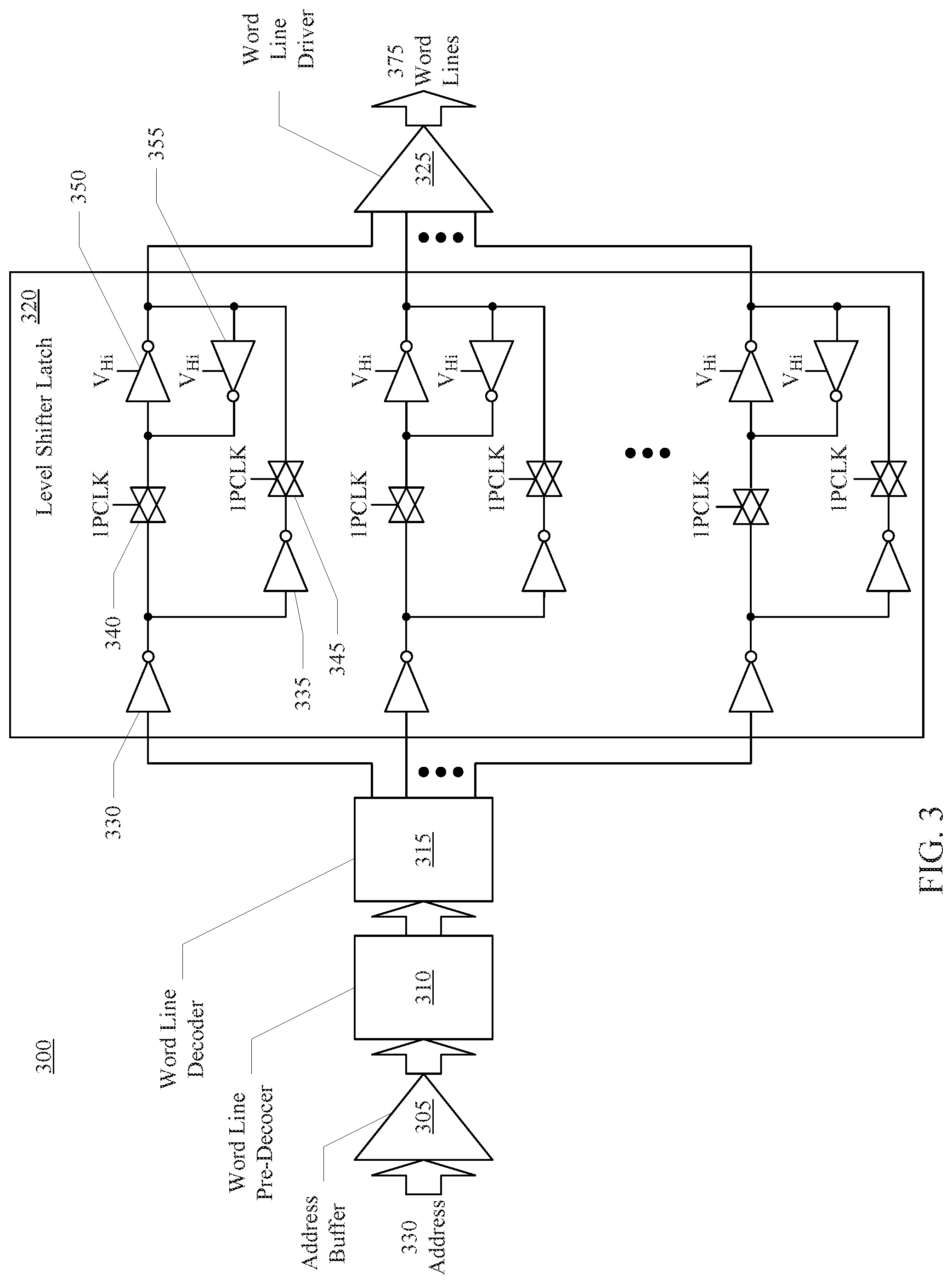
Referring now to FIG. 3, a block diagram of a word line decoder and driver path architecture, in accordance with aspects of the present technology, is shown. In some aspects, the word line decoder and driver path architecture 300 can include an address buffer 305, a word line pre-decoder 310, a word line decoder 315, a level shifter latch 320, and a word line driver 325. The address buffer 305 can be configured to receive and buffer a plurality of address signals 330. The word line pre-decoder 310 can be configured to receive the buffered plurality of address signals and output partially decoded address signals. In one implementation, the word line pre-decoder 310 can be configured to decode a block, bank and/or the like portion of the memory from the buffered plurality of address signals. The word line decoder 315 can be configured to receive the partially decoded address signal and output a plurality of decoded address signals. In one implementation, the word line decoder 315 can be configured to decode a given word line from the buffered plurality of address signals. The level shifter latch 320 can be configured to receive the plurality of decoded address signals upon a first state of a clock signal and to output a plurality of word line signals. In one implementation, the plurality of decoded address signals can include one or more of a first potential voltage and a second potential voltage. The plurality of word line signals can include one or more of a third potential voltage and a fourth potential voltage, wherein a potential difference between the third potential voltage and the fourth potential voltage is greater than a potential difference between the first potential voltage and the second potential voltage. For example, the decoded address signals can be signals having either a ground potential state (e.g., low logic state) or a low supply voltage potential (e.g., high logic state). The word line signals can be signals having either a ground potential state (e.g., low drive state) or a high supply voltage potential (e.g., high drive state).
In some aspects, the level shifter latch 320 can include, for each of the plurality of word lines, a first inverter 330, a second inverter 335, a first transmission gate 340, a second transmission gate 345, a third inverter 350, and a fourth inverter 355. The first inverter 330 can including an input configured to receive a first one of the plurality of decoded address signals. The second inverter 335 can include an input coupled to an output of the first inverter 330. The first transmission gate 340 can include a first terminal coupled to the output of the first inverter 330, a second terminal configured to receive a short pulse clock signal (1PCLK), and a third terminal. The second transmission gate 345 can include a first terminal coupled to an output of the second inverter 335, a second terminal configured to receive the short pulse clock signal (1PCLK), and a third terminal. The third inverter 350 can include an input coupled to the third terminal of the first transmission gate 340, power terminals coupled between a high voltage source (V.sub.Hi), and an output terminal configured to output a first one of the plurality of word line signals. The fourth inverter 355 can include an input coupled to the third terminal of the second transmission gate 345 and the output of third inverter 350, power terminals coupled between the high voltage source (V.sub.Hi), and an output terminal coupled to the input of the third inverter 350.
In some aspects, the third and fourth inverter 350, 355 form a bi-stable latch with two stable states. The first transmission gate 340 can pass a complement of the decoded address signal to a first terminal of the bi-stable latch during a given state (e.g., logic high) of the short clock pulse signal, while the second transmission gate 345 can pass the decoded signal to a second terminal of the bi-stable latch. The short pulse clock signal (1PCLK) 410 can be generated based on a rising edge of a system clock (CLK) 420, as illustrated in FIG. 4. The short pulse clock signal at the gate of the first and second transmission gates 340, 345 can transfer the address to the third and fourth inverters 350, 355 at the rising edge of the system clock (CLK) 420. The pulse width of the short pulse clock signal (1PCLK) 410 can extend the hold time of the address. The pulse width of the short pulse clock signal (1PCLK) 410 should be less than the pulse width of the system clock (CLK) 420. The output of the level shifter latch 320 can be taken at the second terminal of the bi-stable latch.
In one implementation, when the decoded address signal is in a logic low state, the first inverter 330 generates a logic high state at its output and the second inverter 335 generates a logic low state at its output. The first pass gate 340 passes the logic high state from the first inverter 330 to an input of the third inverter 350 when the short pulse clock signal (1PCLK) is in a given state (e.g., logic high state), and the second pass gate 345 passes the logic low state from the second inverter 335 to an input of the fourth inverter 355 when the short pulse clock signal (1PCLK) is in the given state. The logic high state at the input to the third inverter 350 and the logic low state at the input to the fourth inverter 355 will drive the output of the bi-stable latch to the low drive state. When the decoded address signal is in a logic high state, the first inverter 330 generates a logic low state at its output and the second inverter 335 generates a logic high state at its output. The first pass gate 340 passes the logic low state from the first inverter 330 to an input of the third inverter 350 when the short pulse clock signal (1PCLK) is in the given state (e.g., logic high state), and the second pass gate 345 passes the logic high state from the second inverter 335 to an input of the fourth inverter 355 when the short pulse clock signal (1PCLK) is in the given state. The logic low state at the input to the third inverter 350 and the logic high state at the input to the fourth inverter 355 will drive the output of the bi-stable latch to the high drive state. The logic level of the decoded address signal (e.g., logic low or logic high) is shifted to the drive level of the word line signal (e.g., low drive state or high drive state) as a result of the high voltage source (V.sub.Hi) supplied to the third and fourth inverters 350, 355 of the bi-stable latch. The level shifted word line signals can be output by the level shifter latch 320. The word line driver 325 can be configured to receive the plurality of word line signals and drive the plurality of word line signals on corresponding ones of the plurality of word lines 375.
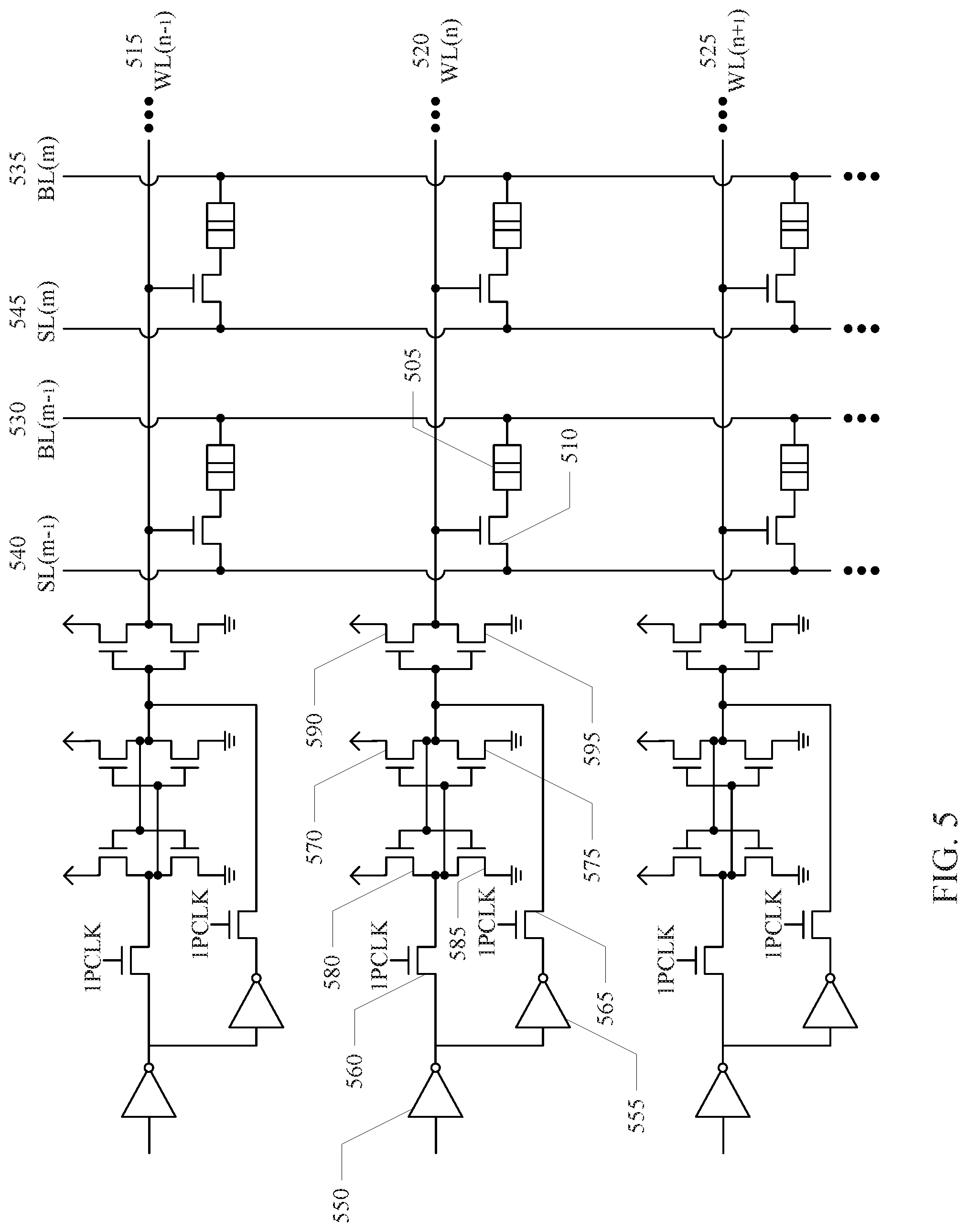
Referring now to FIG. 5, a block diagram of a word line driver in combination with a memory cell array, in accordance with aspects of the present technology, is shown. The memory cell array can be any one of a number of memory cell architectures, such as NAND Flash memory, Magnetoresistive Random Access Memory (MRAM), or the like that can benefit from a fast word line drive circuit due to characteristics such as relatively high capacitive word lines. While aspects of the present technology are described herein in conjunction with MRAM memory cell arrays, it will be understood that they are not intended to be limited thereto.
In some aspects, the MRAM memory cell array can include a plurality of memory cells 505, 510, a plurality of word lines 515-525, a plurality of bit lines 530-535, and a plurality of source lines 540-545. The word lines 515-525 of the memory cell array can be organized along rows of the array. The bit lines 530-535 and the source lines 540-545 can be organized along columns of the array. Each memory cell 505, 510 can include a Magnetic Tunneling Junction (MTJ) cell 505 and an access transistor 510. In one implementation, the MTJ cells can be Spin Torque Magnetoresistive memory cells. The gates of the access transistors 510 arranged along rows of the array can be coupled to a respective word line 520. The sources of the access transistors 510 arranged along columns of the array can be coupled to respective source lines 540. A free magnetic layer of the MTJ cell 505 arranged along columns of the array can be coupled to respective bit lines 530.
In some aspects, the magnetic polarity of the free layer of the MTJ cell 505, and corresponding logic state of the cell, can be changed to one of two states depending upon the direction of current flowing through the MTJ cell 505. For example, a logic `0` state can be written to the memory cell 505, 510 by biasing the respective bit line 530 at a bit line write potential (e.g., V.sub.BLW), biasing the respective source line 540 at a ground potential, and driving the respective word line 520 at a word line write potential (e.g., V.sub.WLW=V.sub.Hi). A logic `1` state can be written to the given memory cell 505, 510 by biasing the respective bit line 530 at a ground potential, biasing the respective source line 540 at a source line write potential (e.g., V.sub.SLW), and driving the respective word line 520 at the word line write potential (e.g., V.sub.WLW=V.sub.Hi). The state of the memory cell 505, 510 can be read by biasing the respective bit line 530 at a bit line read potential (e.g., V.sub.BLR), biasing the respective source line 540 at a ground potential, driving the respective word line 520 at a word line read potential (V.sub.WLR=V.sub.Hi), and sensing the resulting current on the respective bit line 530.
In another example, a logic `0` state can be written to a given memory cell 505, 510 by biasing the respective bit line 530 at a bit line write potential (e.g., V.sub.BLW), biasing the respective source line 540 at a ground potential, and driving the respective word line 520 at a word line write potential (e.g., V.sub.WLW=V.sub.Hi). A logic `1` state can be written to the given memory cell 505, 510 by biasing the respective bit line 530 at a ground potential, biasing the respective source line 540 at a source line write potential (e.g., V.sub.SLW), and driving the respective word line 520 at the word line write potential (e.g., V.sub.WLW=V.sub.Hi). The state of the memory cell 505, 510 can be read by biasing the respective bit line 530 at a ground potential, biasing the respective source line 540 at a source line read potential (e.g., V.sub.SLR), driving the respective word line 520 at a word line read potential (e.g., V.sub.WLR=V.sub.Hi), and sensing the resulting current on the respective source line 540.
In some aspects, the word line driver can include, for each of a plurality of word lines, a first inverter 550, a second inverter 555, a first transmission gate 560, a second transmission gate 565, a level shifter latch 570-585, and an inverting driver 590, 595. The first inverter 550 can include an input configured to receive a decoded address signal. The second inverter 555 can include an input coupled to an output of the first inverter 550. The first and second inverters 550, 555 can operate from a first supply potential.
In some aspects, the first transmission gate 560 can include a control terminal configured to receive a short pulse clock signal (1PCLK) and an input coupled to the output of the first inverter 550. The second transmission gate 565 can include a control terminal configured to receive the short pulse clock signal (1PCLK) and an input coupled to the output of the second inverter 555. Again, the short pulse clock signal (1PCLK) can be generated based on the rising edge of a system clock (CLK). In one implementation, the first and second transmission gates 560, 565 can be first and second Metal Oxide Semiconductor Field Effect Transistors (MOSFETs) respectively. MOSFETs can be either p-channels MOSFETs or n-channels MOSFETs. The first MOSFET 560 can include a gate configured to receive the short pulse clock signal (1PCLK), a source coupled to the output of the first inverter 550, and a drain coupled to the input of the first latch inverter 570, 575. The second MOSFET 565 can include a gate configured to receive the short pulse clock signal (1PCLK), a source coupled to the output of the second inverter 555, and a drain coupled to an input of the second latch inverter 580, 585. In one implementation, first and second MOSFETs 560, 565 can be n-MOSFETs. In other implementations, it may be possible to use transmission gates or buffers in place of the first and second MOSFETs 560, 565.
In some aspects, the level shifter latch 570-585 can include a first latch inverter 570, 575 cross coupled to a second latch inverter 580, 585. An input of the first latch inverter 570, 575 can be coupled to an output of the first clocked transmission gate 560 and an output of the second latch inverter 580, 585. The input of the second latch inverter 580, 585 can be coupled to an output of the second clocked transmission gate 565 and an output of the first latch inverter 570, 575. The level shifter 570-585 can operates from a second supply potential that is greater than the first supply potential. In one implementation, the first latch inverter 570, 575 includes a first p-MOSFET 570 and a first n-MOSFET 575. A gate of the first p-MOSFET 570 and a gate of the first n-MOSFET 575 can be coupled together as the input of the first latch inverter 570, 575, a drain of the first p-MOSFET 570 and a drain of the first n-MOSFET 575 can be coupled together as the output of the first latch inverter 570, 575, and a source of the first p-MOSFET 570 and the source of the first n-MOSFET 575 can be coupled between the second supply potential. The second latch inverter 580, 585 can include a second p-MOSFET 580 and a second n-MOSFET 585. A gate of the second p-MOSFET 580 and a gate of the second n-MOSFET 585 can be coupled together as the input of the second latch inverter 580, 585, a drain of the second p-MOSFET 580 and a drain of the second n-MOSFET 585 can be coupled together as the output of the second latch inverter 580, 585, and a source of the second p-MOSFET 580 and the source of the second n-MOSFET 585 can be coupled between the second supply potential. It should also be appreciated that the drain and source of MOSFET devices are generally interchangeable, such that the description of the sources and drains of MOSFET herein can be interchanged.
In some aspects, the inverting driver 590, 595 can include an input coupled to an output of the first latch inverter 570, 575 and the output of the second clocked transmission gate 565, and an output coupled to a word line (WL(n)) 520. The inverting driver 590, 595 can operate from the second supply potential. In one implementation, the inverting driver 590, 595 can include a p-MOSFET 590 and a n-MOSFET 595. A gate of the p-MOSFET 590 and the gate of the n-MOSFET 595 can be coupled together as the input of the inverting driver 590, 595, a drain of the p-MOSFET 590 and a drain of the n-MOSFET 595 can be coupled together as the output of the inverting driver 590, 595, and a source of the p-MOSFET 590 and a source of the n-MOSFET 595 can be coupled between the second supply potential.
In some aspects, the first inverter 550, the second inverter 555, the first transmission gate 560, the second transmission gate 565, the level shifter 570-585, and the inverting driver 590, 595 of the word line driver can drive the word line 520 when the word line 520 is selected by a decoded address signal. For example, when the decoded address signal is in a logic low state, the first inverter 550 generates a logic high state at its output and the second inverter 555 generates a logic low state at its output. The first transmission gate 560 passes the logic high state from the first inverter 550 to an input of the first latch inverter 570, 575 when the short pulse clock signal (1PCLK) is in a given state (e.g., logic high state), and the second transmission gate 565 passes the logic low state from the second inverter 555 to an input of the second latch inverter 580, 585 when the short pulse clock signal (1PCLK) is in the given state. The logic high state at the input to the first latch inverter 570, 575 and the logic low state at the input to the second latch inverter 580, 585 will drive the output of the bi-stable level shifter latch 570-585 to the low drive state. In response to the low drive state from the level shifter latch 570-585, the inverting driver 590, 595 generates a high drive state to drive the given word line 520 to select the memory cells 505, 510 on the given word line 520. When the decoded address signal is in a logic high state, the first inverter 550 generates a logic low state at its output and the second inverter 555 generates a logic high state at its output. The first pass gate 560 passes the logic low state from the first inverter 550 to an input of the first latch inverter 570, 575 when the short pulse clock signal (1PCLK) is in the given state (e.g., logic high state), and the second pass gate 565 passes the logic high state from the second inverter 555 to an input of the second latch inverter 580, 585 when the short pulse clock signal (1PCLK) is in the given state. The logic low state at the input to the first latch inverter 570, 575 and the logic high state at the input to the second latch inverter 580, 585 will drive the output of the bi-stable level shifter latch 570-585 to the high drive state. The logic level of the decoded address signal (e.g., logic low or logic high) is shifted to the drive level of the word line signal (e.g., low drive state or high drive state) as a result of the high voltage source (V.sub.Hi) supplied to the first and second latch inverters of the bi-stable level shifter latch 570-585. In response to the high drive state from the level shifter latch 570-585, the inverting driver 590-595 generates a low drive state on the given word line 520 to de-select the memory cells 505, 510 on the given word line 520.
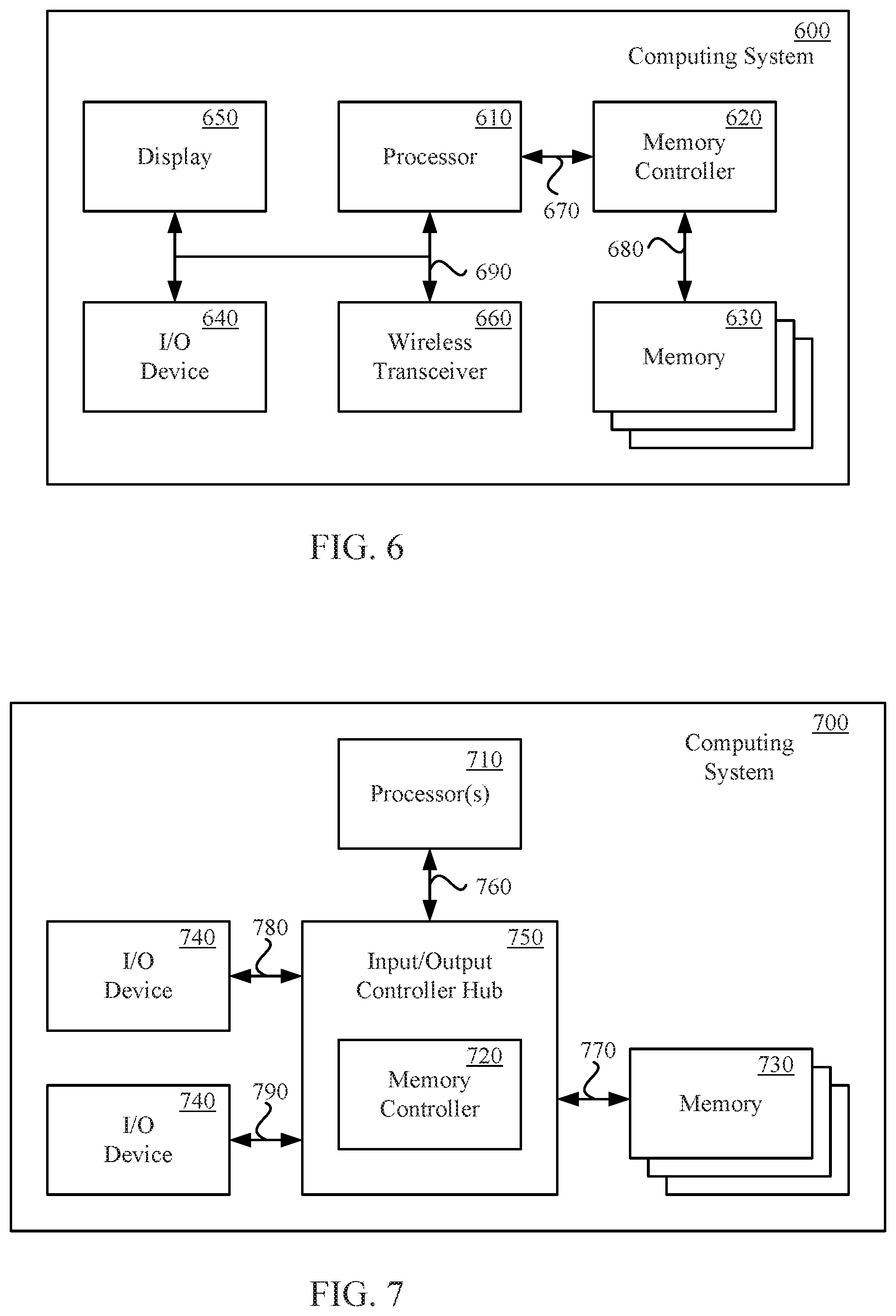
Referring now to FIG. 6, a block diagram of a computing system including a memory device, in accordance with aspects of the present technology, is shown. The computing system 600 can, for example, be a cellular telephone, smart phone, e-reader, tablet personal computer (PC), laptop PC, desktop PC, gaming console, workstation, server computer, or other similar computing device. The computing system 600 can include one or more processors 610, one or more memory controllers 620, one or more memory devices 630, and one or more input/output devices 640-660 communicatively coupled together by one or more buses 670-690. The one or more input/output devices 640 can include, for example, a display 650, a wireless transceiver 660 and the like. The computing system 600 can also include other sub-circuits that are not necessary for an understanding of the present technology and therefore are not discussed herein.
The one or more memory controllers 620 can be operable to control access to data stored in the one or more memory devices 630 for use by the one or more processors 610, one or more input/output devices 640 and/or other sub-systems of the computing system 600. The one or more memory controllers 620 can generate commands for reading and writing of data in the one or more memory devices 630 in response to memory requests received from the one or more processors 610, one or more input/output devices 640 and/or other sub-systems. One or more of the memory devices 630 can include the word line driver circuit as described herein with regard to FIGS. 2-4.
Referring now to FIG. 7, a block diagram of a computing system including a memory device, in accordance with aspects of the present technology, is shown. The computing system 700 can, for example, be a cellular telephone, smart phone, e-reader, table personal computer (PC), laptop PC, desktop PC, gaming console, workstation, server computer, or other similar computing device. The computing system 700 can include one or more processors 710, one or more memory controllers 720, one or more memory devices 730, and one or more input/output devices 740 that can be communicatively coupled together by one or more input/output controller hubs 750 through one or more buses 760-790. The computing system 700 can also include other sub-circuits that are not necessary for an understanding of the present technology and therefore are not discussed herein.
The one or more memory controllers 720 can be integral to one or more other sub-circuits such as the one or more input/output controller hubs 750 and/or memory devices 730, or can be implemented as a separate sub-circuit. The one or more memory controllers 720 can be operable to control access to data stored in the one or more memory devices 730 for use by the one or more processors 710, one or more input/output devices 740 and/or other sub-systems of the computing system 700. The one or more memory controllers 720 can generate commands for reading and writing of data in the one or more memory devices 730 in response to memory requests received from the one or more processors 710, one or more input/output devices 740 and/or other sub-systems. One or more of the memory devices 730 can include the word line driver circuit as described herein. with regard to FIGS. 2-4.
Referring now to FIG. 8, a block diagram of a memory sub-system, in accordance with aspects of the present technology, is shown. The memory sub-system 800 can include one or more memory controllers 810 and one or more memory devices 820. The memory sub-system 800 can be a memory expansion card, Solid State Drive (SSD), or the like that is configurable to be coupled to a host device 830 such as a cellular telephone, smart phone, e-reader, table personal computer (PC), laptop PC, desktop PC, gaming console, workstation, server computer, or other similar computing device. The memory sub-system 800 can be coupled to the host device 830 as in internal or external peripheral device.
The one or more memory controllers 810 can be operable to control access to data stored in the one or more memory devices 820 for use by the host device 830. The one or more memory controllers 810 can generate commands for reading and writing of data in the one or more memory devices 820 in response to memory requests received from the host device 830. One or more of the memory devices 820 can include the word line driver circuit as described herein with regard to FIGS. 2-4.
Referring now to FIG. 9, a block diagram of a memory sub-system, in accordance with aspects of the present technology, is shown. The memory sub-system 900 can include one or more memory devices 910. The memory sub-system 900 can be a memory expansion card, Solid State Drive (SSD), or the like that is configurable to be coupled to a host device 920 such as a cellular telephone, smart phone, e-reader, table personal computer (PC), laptop PC, desktop PC, gaming console, workstation, server computer, or other similar computing device. The host device 920 can include one or more memory controllers 930. The memory sub-system 900 can be coupled to the host device 920 as in internal or external peripheral device.
The one or more memory controllers 930 can be operable to control access to data stored in the one or more memory devices 910 for use by the host device 920. The one or more memory controllers 930 can generate commands for reading and writing of data in the one or more memory devices 910 in response to memory requests received from the host device 920. One or more of the memory devices can include the word line driver circuit 240 as described herein with regard to FIGS. 2-4.
The computing systems and memory sub-systems of FIG. 5-9 are illustrative of exemplary embodiments, and are not intended to limit aspects of the present technology. The word line driver circuit as described herein can be readily applied to any number of conventional memory devices, memory sub-systems, and/or computing systems, along with memory devices, memory sub-systems, and/or computing systems to be developed in the future.
The word line decoder and driver circuit in accordance with aspects of the present technology advantageously reduces delay in the word line driver circuit. In aspects, the address can be decoded and transfer to the level shifter latch as soon as the clock signal is received. The latching function is advantageously moved toward the end of the word line decoder and driver circuit. The delay of the word line decoder and driver circuit in accordance with aspects of the present technology can be the sum of the transmission gate delay and the propagation delay through the level shifter latch and word line driver (e.g., Ttr+Twdr), as compared to the sum of flip flop latch delay, the propagation delay through the address buffer, the propagation delay through the word line pre-decoder, the propagation delay through the word line decoder, and the propagation through the level shifter and word line driver (e.g., Tc.fwdarw.q+Tab+Twpd+Twd+Twdr). Aspects of the present technology also advantageously eliminate the use of a clocked flip flop, which can reduce the area of the word line decoder and driver circuit in the Integrated Circuit (IC) chip of the device.
The foregoing descriptions of specific aspects of the present technology have been presented for purposes of illustration and description. They are not intended to be exhaustive or to limit the invention to the precise forms disclosed, and obviously many modifications and variations are possible in light of the above teaching. The aspects were chosen and described in order to best explain the principles of the present technology and its practical application, to thereby enable others skilled in the art to best utilize the present technology and various aspects with various modifications as are suited to the particular use contemplated. It is intended that the scope of the invention be defined by the claims appended hereto and their equivalents.
* * * * *
D00000
D00001
D00002
D00003
D00004
D00005
D00006
D00007
XML
uspto.report is an independent third-party trademark research tool that is not affiliated, endorsed, or sponsored by the United States Patent and Trademark Office (USPTO) or any other governmental organization. The information provided by uspto.report is based on publicly available data at the time of writing and is intended for informational purposes only.
While we strive to provide accurate and up-to-date information, we do not guarantee the accuracy, completeness, reliability, or suitability of the information displayed on this site. The use of this site is at your own risk. Any reliance you place on such information is therefore strictly at your own risk.
All official trademark data, including owner information, should be verified by visiting the official USPTO website at www.uspto.gov. This site is not intended to replace professional legal advice and should not be used as a substitute for consulting with a legal professional who is knowledgeable about trademark law.