Light-guide device with optical cutoff edge and corresponding production methods
Danziger , et al. O
U.S. patent number 10,437,031 [Application Number 15/996,476] was granted by the patent office on 2019-10-08 for light-guide device with optical cutoff edge and corresponding production methods. This patent grant is currently assigned to LUMUS LTD.. The grantee listed for this patent is LUMUS LTD. Invention is credited to Yochay Danziger, Edgar Friedmann.


View All Diagrams
| United States Patent | 10,437,031 |
| Danziger , et al. | October 8, 2019 |
Light-guide device with optical cutoff edge and corresponding production methods
Abstract
A light-guide device includes a light guiding element (13) with a number of faces, including two parallel faces (26), for guiding light by internal reflection. A transparent optical element (19) has an interface surface for attachment to a coupling surface (14) of the light guiding element, and is configured such that light propagating within the transparent optical element passes through the interface surface and the coupling surface (14) so as to propagate within the light guiding element (13). A non-transparent coating (15) is applied to at least part of one or more faces of the light guiding element (13), defining an edge (17) adjacent to, or overlapping, the coupling surface (14) of the light guiding element (13). A quantity of transparent adhesive is deployed between the coupling surface and the interface surface so as to form an optically transmissive interface. An overspill region 31 of the adhesive extends to, and overlaps, the edge (17).
| Inventors: | Danziger; Yochay (Kfar Vradim, IL), Friedmann; Edgar (Sdey-Acraham, IL) | ||||||||||
|---|---|---|---|---|---|---|---|---|---|---|---|
| Applicant: |
|
||||||||||
| Assignee: | LUMUS LTD. (Ness Ziona,
IL) |
||||||||||
| Family ID: | 62110602 | ||||||||||
| Appl. No.: | 15/996,476 | ||||||||||
| Filed: | June 3, 2018 |
Prior Publication Data
| Document Identifier | Publication Date | |
|---|---|---|
| US 20180275384 A1 | Sep 27, 2018 | |
Related U.S. Patent Documents
| Application Number | Filing Date | Patent Number | Issue Date | ||
|---|---|---|---|---|---|
| PCT/IL2017/051217 | Nov 8, 2017 | ||||
| PCT/IL2017/051028 | Sep 12, 2017 | ||||
| 62418919 | Nov 8, 2016 | ||||
| 62509369 | May 22, 2017 | ||||
| 62535890 | Jul 23, 2017 | ||||
| Current U.S. Class: | 1/1 |
| Current CPC Class: | G02B 17/086 (20130101); G02B 6/34 (20130101); B29D 11/00875 (20130101); G02B 17/00 (20130101); B29D 11/00663 (20130101); G02B 1/10 (20130101); G02B 6/30 (20130101) |
| Current International Class: | G02B 17/08 (20060101); G02B 6/34 (20060101); G02B 17/00 (20060101); G02B 6/30 (20060101); G02B 1/10 (20150101); B29D 11/00 (20060101) |
| Field of Search: | ;359/834 |
References Cited [Referenced By]
U.S. Patent Documents
| 2748659 | June 1956 | Geffcken et al. |
| 2795069 | June 1957 | Hardesty |
| 2886911 | May 1959 | Hardesty |
| 2958258 | November 1960 | Kelly |
| 3491245 | January 1970 | Hardesty |
| 3626394 | December 1971 | Nelson |
| 3658405 | April 1972 | Pluta |
| 3667621 | June 1972 | Barlow |
| 3677621 | July 1972 | Smith |
| 3737212 | June 1973 | Antonson et al. |
| 3802763 | April 1974 | Cook et al. |
| 3857109 | December 1974 | Pilloff |
| 3873209 | March 1975 | Schinke |
| 3940204 | February 1976 | Withrington |
| 4084883 | April 1978 | Eastman et al. |
| 4191446 | March 1980 | Arditty et al. |
| 4240738 | December 1980 | Praamsma |
| 4309070 | January 1982 | St Leger Searle |
| 4331387 | May 1982 | Wentz |
| 4355864 | October 1982 | Soref |
| 4372639 | February 1983 | Johnson |
| 4383740 | May 1983 | Bordovsky |
| 4516828 | May 1985 | Steele |
| 4613216 | September 1986 | Herbec et al. |
| 4711512 | December 1987 | Upatnieks |
| 4715684 | December 1987 | Gagnon |
| 4755667 | July 1988 | Marsoner et al. |
| 4775217 | October 1988 | Ellis |
| 4798448 | January 1989 | Van Raalte |
| 4799765 | January 1989 | Ferrer |
| 4805988 | February 1989 | Dones |
| 4932743 | June 1990 | Isobe et al. |
| 4978952 | December 1990 | Irwin |
| 5033828 | July 1991 | Haruta |
| 5076664 | December 1991 | Migozzi |
| 5096520 | March 1992 | Faris |
| 5157526 | October 1992 | Kondo et al. |
| 5231642 | July 1993 | Scifres et al. |
| 5278532 | January 1994 | Hegg et al. |
| 5301067 | April 1994 | Bleier et al. |
| 5353134 | October 1994 | Michel et al. |
| 5367399 | November 1994 | Kramer |
| 5369415 | November 1994 | Richard et al. |
| 5453877 | September 1995 | Gerbe et al. |
| 5481385 | January 1996 | Zimmerman et al. |
| 5499138 | March 1996 | Iba |
| 5537260 | July 1996 | Williamson |
| 5539578 | July 1996 | Togino et al. |
| 5543877 | August 1996 | Takashi et al. |
| 5555329 | September 1996 | Kuper |
| 5594830 | January 1997 | Winston et al. |
| 5619601 | April 1997 | Akashi et al. |
| 5650873 | July 1997 | Gal et al. |
| 5680209 | October 1997 | Machler |
| 5724163 | March 1998 | David |
| 5751480 | May 1998 | Kitagishi |
| 5764412 | June 1998 | Suzuki et al. |
| 5808800 | September 1998 | Handschy |
| 5829854 | November 1998 | Jones |
| 5883684 | March 1999 | Millikan et al. |
| 5896232 | April 1999 | Budd et al. |
| 5909325 | June 1999 | Kuba et al. |
| 5919601 | July 1999 | Nguyen et al. |
| 5966223 | October 1999 | Amitai et al. |
| 5982536 | November 1999 | Swan |
| 6007225 | December 1999 | Ramer et al. |
| 6021239 | February 2000 | Minami et al. |
| 6034750 | March 2000 | Rai et al. |
| 6052500 | April 2000 | Takano et al. |
| 6091548 | July 2000 | Chen |
| 6144347 | November 2000 | Mizoguchi et al. |
| 6204975 | March 2001 | Watters et al. |
| 6222676 | April 2001 | Togino et al. |
| 6256151 | July 2001 | Ma et al. |
| 6310713 | October 2001 | Doany et al. |
| 6322256 | November 2001 | Inada et al. |
| 6324330 | November 2001 | Stites |
| 6349001 | February 2002 | Spitzer |
| 6362861 | March 2002 | Hertz et al. |
| 6384982 | May 2002 | Spitzer |
| 6388814 | May 2002 | Tanaka |
| 6404550 | June 2002 | Yajima |
| 6404947 | June 2002 | Matsuda |
| 6406149 | June 2002 | Okuyama |
| 6433339 | August 2002 | Maeda et al. |
| 6490104 | December 2002 | Gleckman et al. |
| 6509982 | January 2003 | Steiner |
| 6542307 | April 2003 | Gleckman |
| 6547423 | April 2003 | Marshall et al. |
| 6556282 | April 2003 | Jamieson et al. |
| 6577411 | June 2003 | Yair |
| 6580529 | June 2003 | Amitai et al. |
| 6606173 | August 2003 | Kappel et al. |
| 6671100 | December 2003 | McRuer |
| 6690513 | February 2004 | Hulse et al. |
| 6704052 | March 2004 | Togino et al. |
| 6704065 | March 2004 | Sharp et al. |
| 6710902 | March 2004 | Takeyama |
| 6775432 | August 2004 | Basu |
| 6791760 | September 2004 | Janeczko et al. |
| 6798579 | September 2004 | Robinson et al. |
| 6825987 | November 2004 | Repetto et al. |
| 6829095 | December 2004 | Amitai |
| 6879443 | April 2005 | Spitzer et al. |
| 6942925 | September 2005 | Lazarev et al. |
| 6950220 | September 2005 | Abramson |
| 6992718 | January 2006 | Takahara |
| 7016113 | March 2006 | Choi et al. |
| 7021777 | April 2006 | Amitai |
| 7025464 | April 2006 | Beeson et al. |
| 7088664 | August 2006 | Kim et al. |
| 7163291 | January 2007 | Cado et al. |
| 7175304 | February 2007 | Wadia et al. |
| 7205960 | April 2007 | David |
| 7206133 | April 2007 | Cassarly |
| 7285903 | October 2007 | Cull et al. |
| 7339742 | March 2008 | Amitai et al. |
| 7355795 | April 2008 | Yamazaki et al. |
| 7391573 | June 2008 | Amitai |
| 7392917 | July 2008 | Alalu et al. |
| 7418170 | August 2008 | Mukawa et al. |
| 7430355 | September 2008 | Heikenfeld et al. |
| 7448170 | November 2008 | Skendzic et al. |
| 7457040 | November 2008 | Amitai |
| 7554737 | June 2009 | Knox et al. |
| 7576916 | August 2009 | Amitai |
| 7576918 | August 2009 | Goggins |
| 7576932 | August 2009 | Vandorpe |
| 7577326 | August 2009 | Amitai |
| 7643214 | January 2010 | Amitai |
| 7672055 | March 2010 | Amitai |
| 7710655 | May 2010 | Freeman et al. |
| 7724441 | May 2010 | Amitai |
| 7724443 | May 2010 | Amitai |
| 7751122 | July 2010 | Amitai |
| 7778508 | August 2010 | Hirayama |
| 7884985 | February 2011 | Amitai et al. |
| 7949214 | May 2011 | Dejong |
| 7995275 | August 2011 | Maeda et al. |
| 8000020 | August 2011 | Amitai |
| 8004765 | August 2011 | Amitai |
| 8035872 | October 2011 | Ouchi |
| 8098439 | January 2012 | Amitai et al. |
| 8369019 | February 2013 | Baker |
| 8405573 | March 2013 | Lapidot et al. |
| 8432614 | April 2013 | Amitai |
| 8643948 | February 2014 | Amitai et al. |
| 8655178 | February 2014 | Capron et al. |
| 8665178 | March 2014 | Wang |
| 8666208 | March 2014 | Amirparviz |
| 8736963 | May 2014 | Robbins et al. |
| 8743464 | June 2014 | Amirparviz |
| 8783893 | July 2014 | Seurin et al. |
| 8786519 | July 2014 | Blumenfeld et al. |
| 8810914 | August 2014 | Amitai et al. |
| 8854734 | October 2014 | Ingram |
| 8861081 | October 2014 | Amitai et al. |
| 8902503 | December 2014 | Amitai et al. |
| 8913865 | December 2014 | Bennett |
| 8965152 | February 2015 | Simmonds |
| 8988776 | March 2015 | Weber et al. |
| 9025253 | May 2015 | Hadad et al. |
| 9069180 | June 2015 | Amitai |
| 9104036 | August 2015 | Amitai et al. |
| 9207457 | December 2015 | Amitai |
| 9248616 | February 2016 | Amitai |
| 9279986 | March 2016 | Amitai |
| 9316832 | April 2016 | Amitai et al. |
| 9417453 | August 2016 | Amitai et al. |
| 9448408 | September 2016 | Amitai et al. |
| 9488840 | November 2016 | Mansharof et al. |
| 9500869 | November 2016 | Amitai |
| 9513481 | December 2016 | Levin et al. |
| 9551880 | January 2017 | Amitai |
| 9568738 | February 2017 | Mansharof et al. |
| 9664910 | May 2017 | Mansharof et al. |
| 9740013 | August 2017 | Amitai et al. |
| 9804396 | October 2017 | Amitai |
| 9805633 | October 2017 | Zheng |
| 9933684 | April 2018 | Brown et al. |
| 10048499 | August 2018 | Amitai |
| 2001/0013972 | August 2001 | Doany et al. |
| 2001/0030860 | October 2001 | Kimura et al. |
| 2001/0055152 | December 2001 | Richards |
| 2002/0015233 | February 2002 | Park |
| 2002/0080622 | June 2002 | Pashley et al. |
| 2002/0085281 | July 2002 | Dubin et al. |
| 2002/0186179 | December 2002 | Knowles |
| 2002/0191297 | December 2002 | Gleckman et al. |
| 2003/0007157 | January 2003 | Hulse et al. |
| 2003/0020006 | January 2003 | Janeczko et al. |
| 2003/0030912 | February 2003 | Gleckman et al. |
| 2003/0063042 | April 2003 | Friesem et al. |
| 2003/0090439 | May 2003 | Spitzer et al. |
| 2003/0165017 | September 2003 | Amitai et al. |
| 2003/0197938 | October 2003 | Schmidt et al. |
| 2003/0218718 | November 2003 | Moliton et al. |
| 2004/0080718 | April 2004 | Kojima |
| 2004/0085649 | May 2004 | Repetto |
| 2004/0136082 | July 2004 | Cado et al. |
| 2004/0137189 | July 2004 | Tellini et al. |
| 2004/0218271 | November 2004 | Hartmaier et al. |
| 2004/0233534 | November 2004 | Nakanishi et al. |
| 2004/0263842 | December 2004 | Puppels et al. |
| 2004/0264185 | December 2004 | Grotsch et al. |
| 2005/0018308 | January 2005 | Cassarly et al. |
| 2005/0023545 | February 2005 | Camras et al. |
| 2005/0083592 | April 2005 | Amitai et al. |
| 2005/0084210 | April 2005 | Cha |
| 2005/0173719 | August 2005 | Yonekubo et al. |
| 2005/0174641 | August 2005 | Greenberg |
| 2005/0174653 | August 2005 | Long |
| 2005/0180687 | August 2005 | Amitai et al. |
| 2005/0265044 | December 2005 | Chen et al. |
| 2006/0091784 | May 2006 | Conner et al. |
| 2006/0126182 | June 2006 | Levola |
| 2006/0132914 | June 2006 | Weiss et al. |
| 2006/0268421 | November 2006 | Shimizu et al. |
| 2007/0070859 | March 2007 | Hirayama |
| 2007/0091445 | April 2007 | Amitai |
| 2007/0153344 | July 2007 | Lin |
| 2007/0159673 | July 2007 | Freeman et al. |
| 2007/0188837 | August 2007 | Shimizu et al. |
| 2007/0206390 | September 2007 | Brukilacchio et al. |
| 2007/0284565 | December 2007 | Leatherdale et al. |
| 2007/0291491 | December 2007 | Li et al. |
| 2008/0013051 | January 2008 | Glinski et al. |
| 2008/0025667 | January 2008 | Amitai |
| 2008/0030974 | February 2008 | Abu-Ageel |
| 2008/0062686 | March 2008 | Hoelen et al. |
| 2008/0068852 | March 2008 | Goihl |
| 2008/0094586 | April 2008 | Hirayama |
| 2008/0151379 | June 2008 | Amitai |
| 2008/0198471 | August 2008 | Amitai |
| 2008/0198604 | August 2008 | Kim et al. |
| 2008/0278812 | November 2008 | Amitai |
| 2009/0009719 | January 2009 | Ryf |
| 2009/0052047 | February 2009 | Amitai |
| 2009/0122414 | May 2009 | Amitai |
| 2009/0165017 | June 2009 | Syed et al. |
| 2009/0190222 | July 2009 | Simmonds et al. |
| 2009/0275157 | November 2009 | Winberg et al. |
| 2010/0020291 | January 2010 | Kasazumi et al. |
| 2010/0046234 | February 2010 | Abu-Ageel |
| 2010/0067110 | March 2010 | Amitai et al. |
| 2010/0111472 | May 2010 | DeJong |
| 2010/0202048 | August 2010 | Amitai et al. |
| 2010/0202125 | August 2010 | Saccomanno |
| 2010/0202129 | August 2010 | Abu-Ageel |
| 2010/0278480 | November 2010 | Vasylyev et al. |
| 2010/0291489 | November 2010 | Moskovits et al. |
| 2011/0019250 | January 2011 | Aiki et al. |
| 2011/0149547 | June 2011 | Bruzzone et al. |
| 2011/0228511 | September 2011 | Weber |
| 2011/0242661 | October 2011 | Simmonds |
| 2012/0039576 | February 2012 | Dangel et al. |
| 2012/0062998 | March 2012 | Schultz et al. |
| 2012/0069547 | March 2012 | Gielen et al. |
| 2012/0147361 | June 2012 | Mochizuki et al. |
| 2012/0218301 | August 2012 | Miller et al. |
| 2012/0281389 | November 2012 | Panagotacos et al. |
| 2012/0287621 | November 2012 | Lee et al. |
| 2012/0306940 | December 2012 | Machida |
| 2013/0022316 | January 2013 | Pelletier et al. |
| 2013/0120986 | May 2013 | Xi |
| 2013/0141937 | June 2013 | Katsuta et al. |
| 2013/0201690 | August 2013 | Vissenberg et al. |
| 2013/0215361 | August 2013 | Wang |
| 2013/0242392 | September 2013 | Amirparviz et al. |
| 2013/0321432 | December 2013 | Burns et al. |
| 2013/0334504 | December 2013 | Thompson et al. |
| 2014/0003762 | January 2014 | Macnamara |
| 2014/0043688 | February 2014 | Schrader et al. |
| 2014/0177049 | June 2014 | Beck |
| 2014/0185142 | July 2014 | Gupta et al. |
| 2014/0192539 | July 2014 | Yriberri et al. |
| 2014/0226215 | August 2014 | Komatsu et al. |
| 2014/0226361 | August 2014 | Vasylyev |
| 2014/0264420 | September 2014 | Edwards et al. |
| 2014/0334126 | November 2014 | Speier et al. |
| 2015/0009682 | January 2015 | Clough |
| 2015/0016777 | January 2015 | Abovitz et al. |
| 2015/0049486 | February 2015 | Jung et al. |
| 2015/0081313 | March 2015 | Boross et al. |
| 2015/0098206 | April 2015 | Pickard et al. |
| 2015/0103151 | April 2015 | Carls et al. |
| 2015/0138646 | May 2015 | Tatsugi |
| 2015/0153569 | June 2015 | Yonekubo |
| 2015/0160529 | June 2015 | Popovich et al. |
| 2015/0219834 | August 2015 | Nichol et al. |
| 2015/0241619 | August 2015 | Richards et al. |
| 2015/0247617 | September 2015 | Du et al. |
| 2016/0116743 | April 2016 | Amitai |
| 2016/0170214 | June 2016 | Amitai |
| 2016/0215956 | July 2016 | Smith et al. |
| 2016/0234485 | August 2016 | Robbins et al. |
| 2016/0238844 | August 2016 | Dobschal |
| 2016/0341964 | November 2016 | Amitai |
| 2016/0370534 | December 2016 | Liu et al. |
| 2016/0370693 | December 2016 | Watanabe |
| 2017/0045666 | February 2017 | Vasylyev |
| 2017/0045743 | February 2017 | Dobschal et al. |
| 2017/0045744 | February 2017 | Amitai |
| 2017/0075119 | March 2017 | Schultz et al. |
| 2017/0242249 | August 2017 | Wall |
| 2017/0343822 | November 2017 | Border |
| 357371 | Feb 1929 | BE | |||
| 1606712 | Apr 2005 | CN | |||
| 1795399 | Jun 2006 | CN | |||
| 101542346 | Sep 2009 | CN | |||
| 107238928 | Oct 2017 | CN | |||
| 1422172 | Nov 1970 | DE | |||
| 19725262 | Dec 1998 | DE | |||
| 102013106392 | Dec 2014 | DE | |||
| 0365406 | Apr 1990 | EP | |||
| 0380035 | Aug 1990 | EP | |||
| 0399865 | Nov 1990 | EP | |||
| 0543718 | May 1993 | EP | |||
| 0566004 | Oct 1993 | EP | |||
| 0580952 | Feb 1994 | EP | |||
| 1096293 | May 2001 | EP | |||
| 1158336 | Nov 2001 | EP | |||
| 1180711 | Feb 2002 | EP | |||
| 1326102 | Jul 2003 | EP | |||
| 1385023 | Jan 2004 | EP | |||
| 1485747 | Dec 2004 | EP | |||
| 1562066 | Aug 2005 | EP | |||
| 1748305 | Jan 2007 | EP | |||
| 0770818 | Apr 2007 | EP | |||
| 1779159 | May 2007 | EP | |||
| 2530510 | Dec 2012 | EP | |||
| 2558776 | Feb 2013 | EP | |||
| 3347761 | Jul 2018 | EP | |||
| 2496905 | Jun 1982 | FR | |||
| 2638242 | Apr 1990 | FR | |||
| 2721872 | Jan 1996 | FR | |||
| 1321303 | Jun 1973 | GB | |||
| 2220081 | Dec 1989 | GB | |||
| 2272980 | Jun 1994 | GB | |||
| 2278222 | Nov 1994 | GB | |||
| 2278888 | Dec 1994 | GB | |||
| H1994242260 | Mar 1996 | JP | |||
| 2002539498 | Nov 2002 | JP | |||
| 2003140081 | May 2003 | JP | |||
| 2003536102 | Dec 2003 | JP | |||
| 2004527801 | Sep 2004 | JP | |||
| 2005084522 | Mar 2005 | JP | |||
| 2006003872 | Jan 2006 | JP | |||
| 2009515225 | Apr 2009 | JP | |||
| 2010060770 | Mar 2010 | JP | |||
| 2010170606 | Aug 2010 | JP | |||
| 2013076847 | Apr 2013 | JP | |||
| 101470387 | Dec 2014 | KR | |||
| 201809768 | Mar 2018 | TW | |||
| 201809798 | Mar 2018 | TW | |||
| 9314393 | Jul 1993 | WO | |||
| 9510106 | Apr 1995 | WO | |||
| 9815868 | Apr 1998 | WO | |||
| 9952002 | Oct 1999 | WO | |||
| 0004407 | Jan 2000 | WO | |||
| 0055676 | Sep 2000 | WO | |||
| 0063738 | Oct 2000 | WO | |||
| 0127685 | Apr 2001 | WO | |||
| 0195025 | Dec 2001 | WO | |||
| 0195027 | Dec 2001 | WO | |||
| 02082168 | Oct 2002 | WO | |||
| 02088825 | Nov 2002 | WO | |||
| 02097515 | Dec 2002 | WO | |||
| 03058320 | Jul 2003 | WO | |||
| 03081320 | Oct 2003 | WO | |||
| 2004053541 | Jun 2004 | WO | |||
| 2004109349 | Dec 2004 | WO | |||
| 2005024485 | Mar 2005 | WO | |||
| 2005024491 | Mar 2005 | WO | |||
| 2005024969 | Mar 2005 | WO | |||
| 2005093 493 | Oct 2005 | WO | |||
| 2005124427 | Dec 2005 | WO | |||
| 2006013565 | Feb 2006 | WO | |||
| 2006061927 | Jun 2006 | WO | |||
| 2006085308 | Aug 2006 | WO | |||
| 2006085309 | Aug 2006 | WO | |||
| 2006085310 | Aug 2006 | WO | |||
| 2006087709 | Aug 2006 | WO | |||
| 2006098097 | Sep 2006 | WO | |||
| 2007054928 | May 2007 | WO | |||
| 2007093983 | Aug 2007 | WO | |||
| 2008023367 | Feb 2008 | WO | |||
| 2008129539 | Oct 2008 | WO | |||
| 2008149339 | Dec 2008 | WO | |||
| 2009009268 | Jan 2009 | WO | |||
| 2009066408 | May 2009 | WO | |||
| 2009074638 | Jun 2009 | WO | |||
| 2011130720 | Oct 2011 | WO | |||
| 2013065656 | May 2013 | WO | |||
| 2013175465 | Nov 2013 | WO | |||
| 2013188464 | Dec 2013 | WO | |||
| 2014076599 | May 2014 | WO | |||
| 2014155096 | Oct 2014 | WO | |||
| 2015081313 | Jun 2015 | WO | |||
| 2015158828 | Oct 2015 | WO | |||
| 20/6/03251 | Jun 2016 | WO | |||
| 2016132347 | Aug 2016 | WO | |||
| 2017106873 | Jun 2017 | WO | |||
| 2017199232 | Nov 2017 | WO | |||
| 2018138714 | Aug 2018 | WO | |||
Other References
|
Da-Yong et al., "A Continuous Membrance Micro Deformable Mirror Based on Anodic Bonding of SOI to Glass Water", Microsystem Technologies, Micro and Nanosystems Information Storage and Processing Systems, vol. 16, No. 10, May 20, 2010 pp. 1765-1769. cited by applicant. |
Primary Examiner: Beatty; Collin X
Attorney, Agent or Firm: Friedman; Mark M.
Claims
What is claimed is:
1. An apparatus comprising: (a) a light guiding element having a plurality of faces including a pair of parallel faces, said light guiding element being configured for guiding light by internal reflection at said parallel faces, one of said plurality of faces providing a coupling surface; (b) a transparent optical element having an interface surface for attachment to said coupling surface, said transparent optical element being configured such that light propagating within said transparent optical element passes through said interface surface and said coupling surface so as to propagate within the light guiding element; (c) a non-transparent coating applied to at least part of at least one of said parallel faces of said light guiding element, said coating defining an edge adjacent to, or overlapping, said coupling surface of said light guiding element; and (d) a quantity of transparent adhesive deployed between said coupling surface and said interface surface so as to form an optically transmissive interface, said adhesive extending to, and overlapping, said edge, wherein said edge defines an optical cutoff edge for light rays passing from said transparent optical element into said light guiding element, and wherein said non-transparent coating is configured to generate internal reflection at an underlying region of said at least one of said parallel faces.
2. The apparatus of claim 1, wherein said coupling surface is provided on one of said parallel faces.
3. The apparatus of claim 2, wherein said coating extends between said coupling surface and said interface surface.
4. The apparatus of claim 1, wherein said coupling surface is inclined relative to said parallel faces.
5. The apparatus of claim 4, wherein said coupling surface and said parallel face meet at a ground edge, and wherein said edge is non-overlapping with said ground edge.
6. The apparatus of claim 5, wherein said adhesive fills a recess formed between said ground edge and said interface surface.
7. The apparatus of claim 4, wherein said coupling surface is obliquely inclined relative to said parallel faces.
8. The apparatus of claim 4, wherein said coupling surface is perpendicular to said parallel faces.
9. The apparatus of claim 1, wherein said interface surface is larger than said coupling surface.
10. The apparatus of claim 1, wherein said coating is a metal coating.
11. The apparatus of claim 1, wherein said coating is a dielectric coating.
12. The apparatus of claim 1, wherein said transparent optical element is a coupling prism configured to provide an input surface oriented for input of light into said light guiding element.
13. An apparatus comprising: (a) a light guiding element having a plurality of faces including a pair of parallel faces, said light guiding element being configured for guiding light by internal reflection at said parallel faces, one of said plurality of faces providing a coupling surface; (b) a coupling prism having an interface surface adhered to said coupling surface and an input surface for input of light into the light guiding element; and (c) a non-transparent coating applied to at least part of said coupling surface of said light guiding element and extending between said light guiding element and said coupling prism, said coating defining an optical cutoff edge for light passing from said coupling prism through said coupling surface into said light guiding element, and wherein said non-transparent coating is configured to generate internal reflection at an underlying region of said at least one parallel face.
14. The apparatus of claim 13, wherein said coupling prism is adhered to said coupling surface of said light guiding element without adhesive.
15. An apparatus comprising: (a) a light guiding element having a plurality of faces including first and second parallel faces, said light guiding element being configured for guiding light by internal reflection at said first and second parallel faces, one of said plurality of faces providing a coupling surface; (b) a coupling prism having an interface surface for attachment to said coupling surface and an input surface for input of light into the light guiding element; and (c) a quantity of transparent adhesive deployed between said coupling surface and said interface surface so as to form an optically transmissive interface, a part of said quantity of adhesive forming a partial filling of an angled recess between said light guiding element and said coupling prism, wherein an air gap extends along one of said faces of said light guiding element beneath said partial filling, said air gap terminating at an edge within said adhesive so as to define an optical cutoff edge adjacent to said coupling surface of said light guiding element.
16. A method for producing an optical assembly, the method comprising: (a) providing a light guiding element having a plurality of faces including first and second parallel faces, said light guiding element being configured for guiding light by internal reflection at said first and second parallel faces; (b) applying a coating to at least part of at least one of said plurality of faces of said light guiding element; (c) grinding said light guiding element along a plane intersecting said coating so as to simultaneously form a coupling surface of said light guiding element and an edge of said coating; and (d) bonding to said coupling surface an interface surface of a transparent optical element, the transparent optical element being configured such that light propagating within the transparent optical element passes through the interface surface and the coupling surface so as to propagate within the light guiding element, wherein said bonding is performed by applying a quantity of a transparent adhesive between said coupling surface and said interface surface, said quantity of adhesive being applied such that, when said coupling surface and said interface surface are pressed together, an excess of said transparent adhesive overlaps said edge of said coating.
17. The method of claim 16, wherein said coating is a non-transparent coating such that said edge defines an optical cutoff edge.
18. The method of claim 16, further comprising a step of selectively removing said coating so as to leave a cutoff edge defined by an edge of an air-gap formed in said transparent adhesive.
19. A method for producing an optical assembly, the method comprising: (a) providing a light guiding element having a plurality of faces including a pair of parallel faces, said light guiding element being configured for guiding light by internal reflection at said parallel faces, one of said plurality of faces providing a coupling surface; (b) applying a non-transparent coating to at least part of at least one of said parallel faces, said non-transparent coating defining an edge adjacent to, or overlapping, said coupling surface of said light guiding element; and (c) bonding to said coupling surface an interface surface of a transparent optical element, the transparent optical element being configured such that light propagating within the transparent optical element passes through the interface surface and the coupling surface so as to propagate within the light guiding element, wherein said bonding is performed by applying a quantity of a transparent adhesive between said coupling surface and said interface surface, said quantity of adhesive being applied such that, when said coupling surface and said interface surface are pressed together, an excess of said transparent adhesive overlaps said edge of said coating, and wherein said edge defines an optical cutoff edge for light rays passing from said transparent optical element into said light guiding element, and wherein said non-transparent coating is configured to generate internal reflection at an underlying region of said at least one parallel face including where overlapped by the excess of said transparent adhesive.
20. The method of claim 19, wherein said coupling surface is provided on one of said parallel faces.
Description
FIELD AND BACKGROUND OF THE INVENTION
The present invention relates to light-guide devices and, in particular, it concerns a light guide device which has a well-defined optical cutoff edge, and corresponding methods for producing such devices.
When manufacturing optical devices, it is often desirable to provide a light guiding device with a complex form in which different regions have surfaces angled with selected non-rectilinear orientations. Examples of such devices relevant to the present invention include, but are not limited to, light guiding elements with coupling-in configurations, and regions of transition between light guiding elements with different transverse dimensions and/or different orientations.
FIGS. 1A and 1B illustrate two examples of devices which include a light guiding element together with a coupling-in prism corresponding to FIGS. 3 and 7, respectively, of PCT Publication No. WO 2015/162611. Referring to the original reference numerals of those drawings in parentheses, each of these devices has a light guiding element (20) with first and second parallel faces (26), and a coupling prism (44, 54) for attachment to the light guiding element so as to provide a suitably angled input surface so that light can be introduced close to the normal to a surface (46, 58) of the prism and then enter the light guide at an angle desired for internal propagation of the light by internal reflection at surfaces (26).
SUMMARY OF THE INVENTION
The present invention is a light guide device and corresponding production methods.
According to the teachings of an embodiment of the present invention there is provided, an apparatus comprising: (a) a light guiding element having a plurality of faces including first and second parallel faces, the light guiding element being configured for guiding light by internal reflection at the first and second parallel faces, one of the plurality of faces providing a coupling surface; (b) a transparent optical element having an interface surface for attachment to the coupling surface, the transparent optical element being configured such that light propagating within the transparent optical element passes through the interface surface and the coupling surface so as to propagate within the light guiding element; (c) a non-transparent coating applied to at least part of at least one of the plurality of faces of the light guiding element, the coating defining an edge adjacent to, or overlapping, the coupling surface of the light guiding element; and (d) a quantity of transparent adhesive deployed between the coupling surface and the interface surface so as to form an optically transmissive interface, the adhesive extending to, and partially overlapping, the edge.
According to a further feature of an embodiment of the present invention, the coupling surface is provided on one of the first and second parallel faces.
According to a further feature of an embodiment of the present invention, the coating extends between the coupling surface and the interface surface.
According to a further feature of an embodiment of the present invention, the coupling surface is inclined relative to the first and second parallel faces.
According to a further feature of an embodiment of the present invention, the coupling surface and the first parallel face meet at a ground edge, and wherein the edge is non-overlapping with the ground edge.
According to a further feature of an embodiment of the present invention, the adhesive fills a recess formed between the ground edge and the interface surface.
According to a further feature of an embodiment of the present invention, the coupling surface is obliquely inclined relative to the first and second parallel faces.
According to a further feature of an embodiment of the present invention, the coupling surface is perpendicular to the first and second parallel faces.
According to a further feature of an embodiment of the present invention, the interface surface is larger than the coupling surface.
According to a further feature of an embodiment of the present invention, the coating is a metal coating.
According to a further feature of an embodiment of the present invention, the coating is a dielectric coating.
According to a further feature of an embodiment of the present invention, the transparent optical element is a coupling prism configured to provide an input surface oriented for input of light into the light guiding element.
According to a further feature of an embodiment of the present invention, the edge defines an optical cutoff edge for light rays passing from the transparent optical element into the light guiding element.
There is also provided according to the teachings of an embodiment of the present invention, an apparatus comprising: (a) a light guiding element having a plurality of faces including first and second parallel faces, the light guiding element being configured for guiding light by internal reflection at the first and second parallel faces, one of the plurality of faces providing a coupling surface; (b) a coupling prism having an interface surface adhered to the coupling surface and an input surface for input of light into the light guiding element; and (c) a non-transparent coating applied to at least part of the coupling surface of the light guiding element and extending between the light guiding element and the coupling prism, the coating defining an optical cutoff edge for light passing from the coupling prism through the coupling surface into the light guiding element.
According to a further feature of an embodiment of the present invention, the coupling prism is adhered to the coupling surface of the light guiding element without adhesive.
There is also provided according to the teachings of an embodiment of the present invention, an apparatus comprising: (a) a light guiding element having a plurality of faces including first and second parallel faces, the light guiding element being configured for guiding light by internal reflection at the first and second parallel faces, one of the plurality of faces providing a coupling surface; (b) a coupling prism having an interface surface for attachment to the coupling surface and an input surface for input of light into the light guiding element; and (c) a quantity of transparent adhesive deployed between the coupling surface and the interface surface so as to form an optically transmissive interface, a part of the quantity of adhesive forming a partial filling of an angled recess between the light guiding element and the coupling prism, wherein an air gap extends along one of the faces of the light guiding element beneath the partial filling, the air gap terminating at an edge within the adhesive so as to define an optical cutoff edge adjacent to the coupling surface of the light guiding element.
There is also provided according to the teachings of an embodiment of the present invention, a method for producing an optical assembly, the method comprising: (a) providing a light guiding element having a plurality of faces including first and second parallel faces, the light guiding element being configured for guiding light by internal reflection at the first and second parallel faces; (b) applying a coating to at least part of at least one of the plurality of faces of the light guiding element; (c) grinding the light guiding element along a plane intersecting the coating so as to simultaneously form a coupling surface of the light guiding element and an edge of the coating; and (d) bonding to the coupling surface an interface surface of a transparent optical element, the transparent optical element being configured such that light propagating within the transparent optical element passes through the interface surface and the coupling surface so as to propagate within the light guiding element, wherein the bonding is performed by applying a quantity of a transparent adhesive between the coupling surface and the interface surface, the quantity of adhesive being applied such that, when the coupling surface and the interface surface are pressed together, an excess of the transparent adhesive overlaps the edge of the coating.
According to a further feature of an embodiment of the present invention, the coating is a non-transparent coating such that the edge defines an optical cutoff edge.
According to a further feature of an embodiment of the present invention, there is also provided a step of selectively removing the coating so as to leave a cutoff edge defined by an edge of an air-gap formed in the transparent adhesive.
BRIEF DESCRIPTION OF THE DRAWINGS
The invention is herein described, by way of example only, with reference to the accompanying drawings, wherein:
FIGS. 1A and 1B, described above, correspond to FIGS. 3 and 7, respectively, of PCT Publication No. WO 2015/162611, illustrating light guide devices to which the present invention may advantageously be applied;
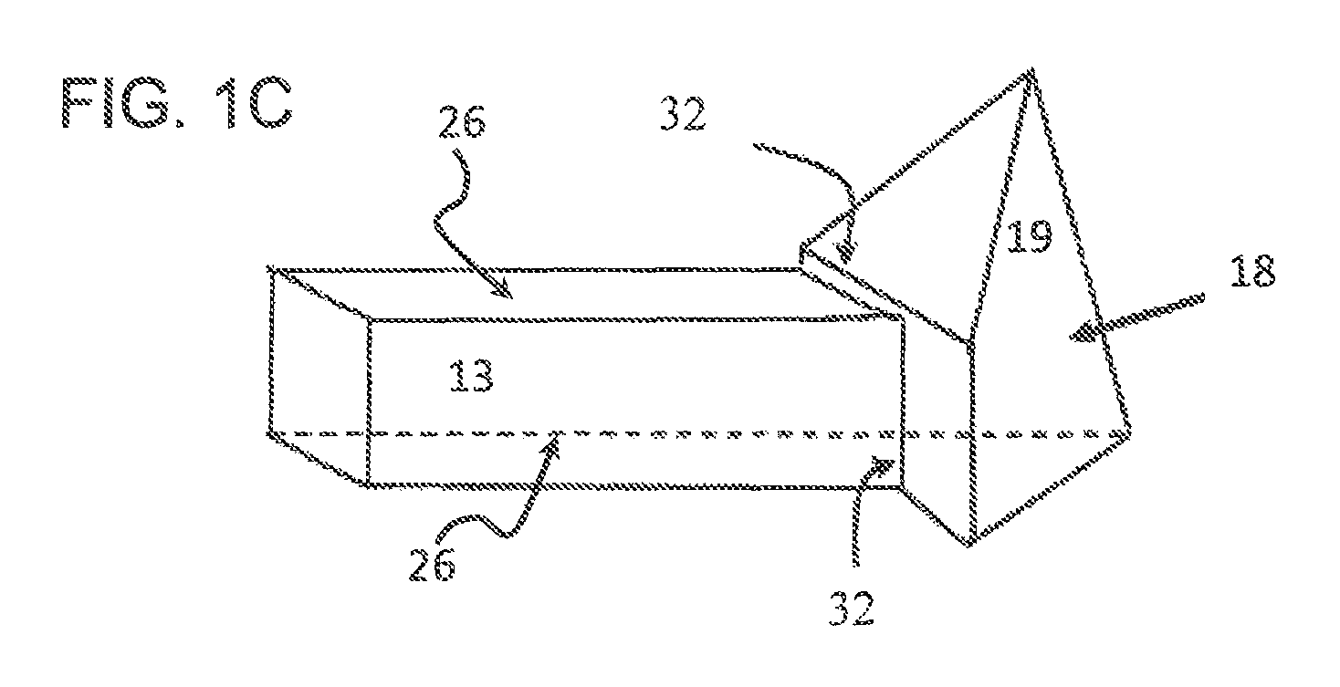
FIG. 1C is a schematic isometric view of a light guide device according to an aspect of the present invention in which context the present invention may also be advantageously applied;
FIGS. 2A, 2B and 2C are schematic enlarged cross-sectional partial views of a region of joining of two transparent optical elements illustrating, respectively, the junction without adhesive, with adhesive, and with a protective layer overlapped by adhesive according to an embodiment of the present invention, each view illustrating various light ray paths for each case;
FIGS. 3A-3C are a sequence of schematic isometric views illustrating stages during the production of a light guide device according to an embodiment of the present invention, the views illustrating a light guiding element after application of a coating, after grinding of a coupling surface, and after bonding of a coupling-in prism, respectively;
FIG. 3D is a schematic isometric view of a light guiding element after application of a coating with a pre-formed edge according to an alternative production sequence of certain embodiments of the present invention;
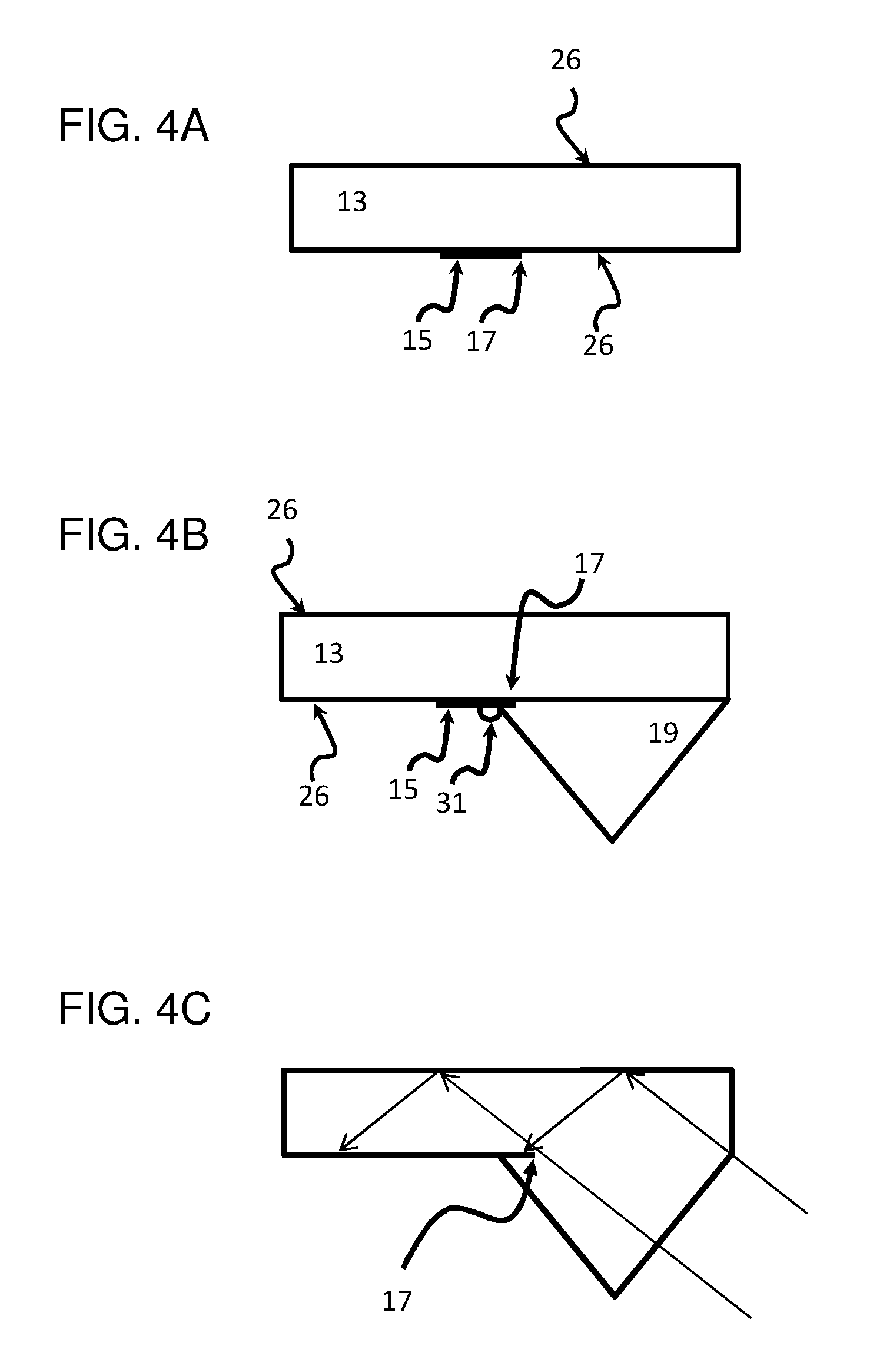
FIGS. 4A and 4B are schematic side views illustrating stages during the production of a further embodiment of the present invention illustrating a light guiding element after application of a coating, and after bonding of a coupling-in prism, respectively;
FIG. 4C is a view similar to FIG. 4B illustrating the overall optical effect of a device resulting from the production process of FIGS. 4A and 4B;
FIGS. 5A-5C are schematic side views illustrating stages during the production of a variant implementation of the device of FIG. 4C;
FIGS. 6A-6C are a sequence of schematic isometric views illustrating stages during the production of a light guide device according to a further embodiment of the present invention, the views illustrating a light guiding element after application of a coating, after grinding of a coupling surface, and after bonding of a coupling-in prism, respectively;
FIG. 6D is a view similar to FIG. 6C illustrating the overall optical effect of a device resulting from the production process of FIGS. 6A-6C;
FIG. 7A is a view similar to FIG. 2C illustrating a further variation of the present invention according to which a coating layer is removed to leave an air gap;
FIG. 7B is a view similar to FIG. 6D illustrating an implementation of that device using an air gap according to FIG. 7A;
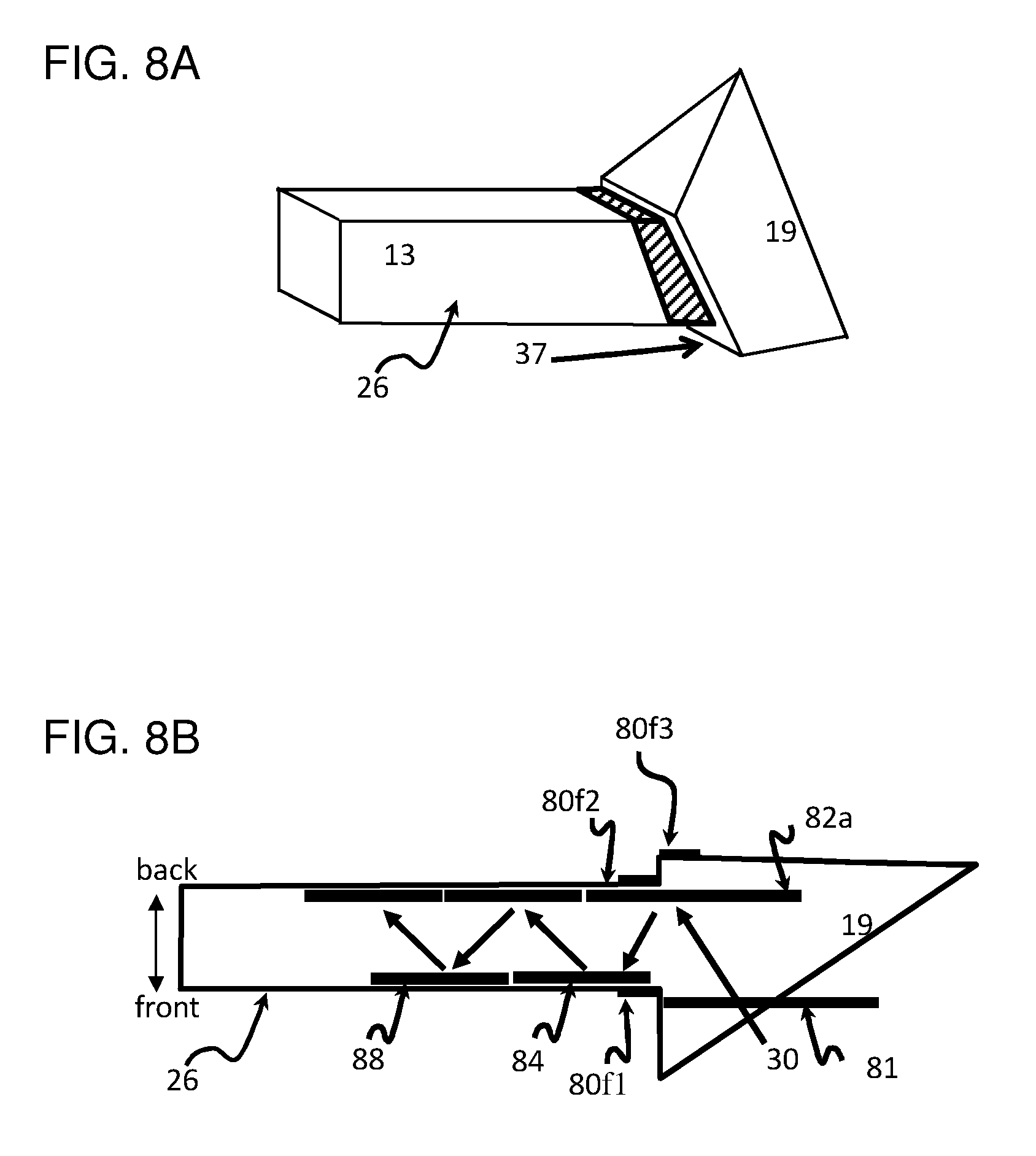
FIG. 8A is an isometric view of a light guide device that is a further variant of the devices of FIGS. 1C and 3C, constructed and operative according to the teachings of an embodiment of the present invention;
FIG. 8B is a schematic horizontal cross-sectional view taken through the device of FIG. 8A adjacent to the base of the light guiding element, illustrating propagation of an input image aperture along the light guiding element; and
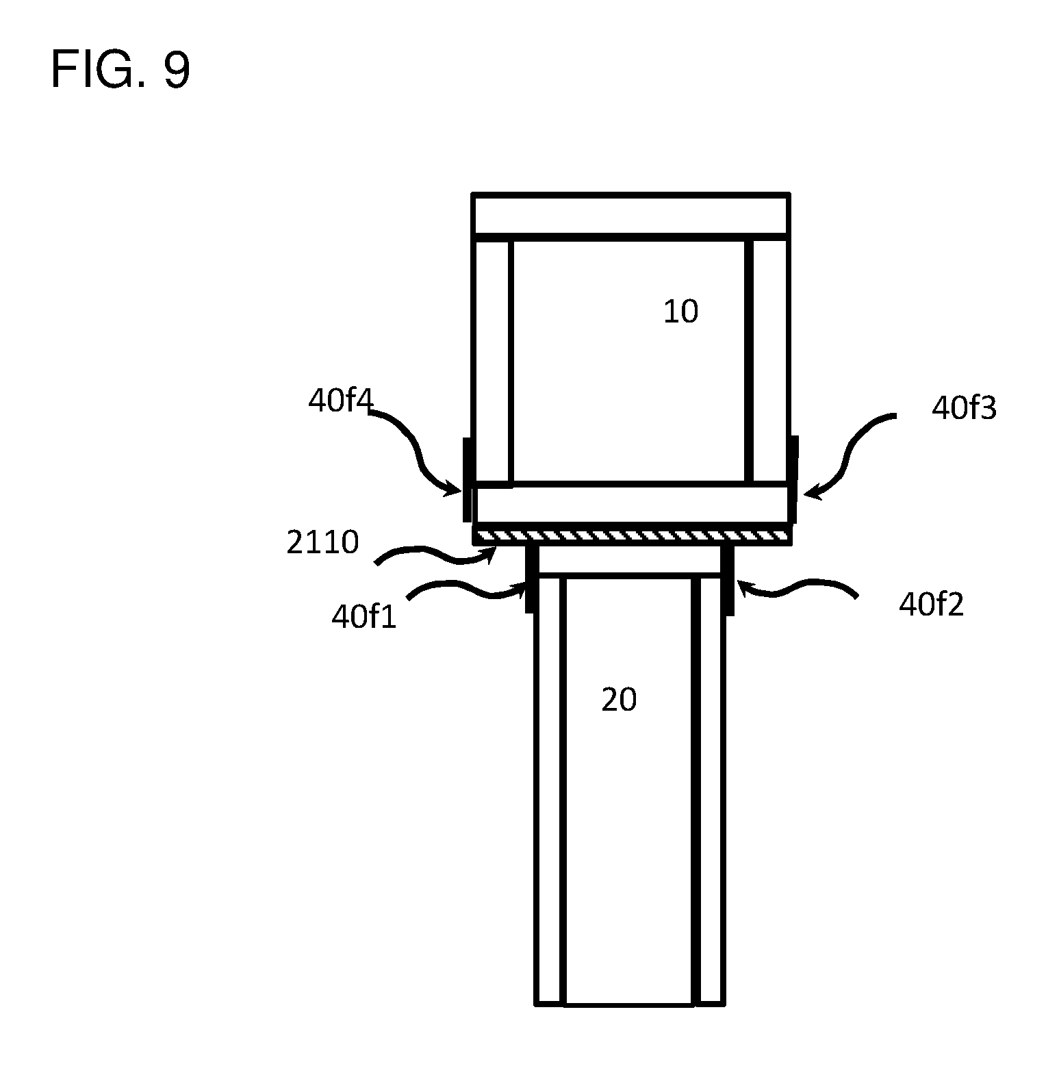
FIG. 9 is a schematic end view of a light guide device formed from superposition of two light guiding elements, implemented according to the teachings of an aspect of the present invention.
DESCRIPTION OF THE PREFERRED EMBODIMENTS
The present invention is a light guide device and corresponding production methods.
The principles and operation of light guide devices according to the present invention may be better understood with reference to the drawings and the accompanying description.
By way of introduction, the present invention relates to a wide range of situations in which two transparent elements are joined, and especially, although not exclusively, where external surfaces of the two elements meet at an angle or step. Joints between transparent elements of an optical system present a number of challenges for practical implementation. Firstly, edges of blocks of transparent material are not perfectly sharp edges, and are modified (distorted) by some radius of curvature, often with some chipping or other defects. The extent of this rounding typically varies depending on the properties of the materials and the type of equipment used. FIG. 2A illustrates a schematic partial cross-sectional enlarged view of a region of joining of two transparent optical elements 13 and 19, where an edge 32 of one of the elements 13 after grinding exhibits a radius of curvature. This radius of curvature results in various scattering effects which reduce the overall quality of the optical device. Thus, while rays R11 and R13 pass from optical element 19 to optical element 13 without scattering and propagate as intended along optical element 13, and ray R15 is excluded from optical element 13, rays R12 and R14 interact with various intermediate angles of the surface due to the rounding of edge 32, resulting in scattering of rays at angles other than those corresponding to the device design, with a consequent reduction in signal-to-noise for the overall device.
A further problem arises through the use of optical adhesives, as illustrated here in FIG. 2B. In order to ensure uniform optical properties at the interface, a sufficient quantity of optical adhesive is interposed between the facing surfaces that, after pressing them together, the entire area of the facing surfaces to be joined is covered with adhesive. This typically leads to some outflow of excess adhesive at the extremities of the surfaces to be joined, forming an overspill region 31 which may be of arbitrary size and uncontrolled shape. Since the adhesive is transparent adhesive, and typically also index-matched to the transparent optical elements, overspill region 31 defines additional paths of optical rays which may result in scattering and unwanted angles of ray propagation within optical element 13. Thus, in the example illustrated here, rays R23 and R24 pass from optical element 19 to optical element 13 without scattering and propagate as intended along optical element 13, and ray R22 escapes without reaching optical element 13. However rays R21 and R25 interact with various arbitrarily-angled surfaces of overspill region 31 of the adhesive, resulting in scattering of rays at angles other than those corresponding to the device design, with a consequent reduction in signal-to-noise for the overall device.
According to one aspect of the present invention, as illustrated in FIG. 2C, there is provided an optical device or apparatus which includes two transparent optical elements, typically a light guiding element 13 with a plurality of faces including first and second parallel faces 26 so that light can be guided within element 13 by internal reflection at first and second parallel faces 26. The second transparent optical element 19 has an interface surface for attachment to a coupling surface of light guiding element 13. A non-transparent (opaque) coating 15 is applied to at least part of at least one of the faces of light guiding element 13, in this case, one of the parallel faces 26. Coating 15 is preferably chosen to provide (or maintain) reflective properties for internal reflection at the surface of the light guiding element, and preferably defines an edge 17 adjacent to, or in some cases described below overlapping, the coupling surface of light guiding element 13. A quantity of transparent adhesive is deployed between the coupling surface and the interface surface so as to form an optically transmissive interface, the adhesive forming an overspill region 31 which extends to, and partially overlaps, the edge 17.
As seen in FIG. 2C, the presence of coating 15 according to this exemplary implementation significantly enhances the optical properties of the device. Firstly, due to the presence of coating 15 on the surface of light guiding element 13, the adhesive of overspill region 31 does not compromise the internal reflection properties of the light guiding element 13, such that ray R31 is internally reflected within the light guiding element and propagates correctly within the light guiding element. Additionally, edge 17 here serves as an optical cutoff edge, cleanly delineating between rays R31, R33 and R34 which enter the light guiding element undistorted, and rays R32 and R35 which are excluded therefrom. Any stray light that is reflected by irregular surfaces of the adhesive overspill region 31, such as ray R35, hits the outer surface of coating 15 and is excluded from the light guiding element.
Coating 15 may be formed from any material suitable for application to a surface of an optical element and which provides the required light-blocking properties and provides internally reflective properties of the transparent optical elements. Examples include, but are not limited to, various metal coatings and various dielectric coatings. In one particularly preferred but non-limiting example, a coating of silver protected by a thin sealing layer to prevent oxidation has been found to be particularly effective and suitable for this application.
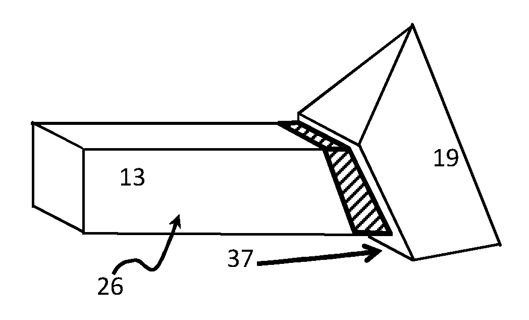
The present invention is applicable to a wide range of applications in which two transparent optical elements are joined together. A subset of applications of particular importance relates to devices in which light is introduced into a light guiding element 13, either from another light guiding element or from a coupling-in configuration 19. Such applications can employ a number of different geometries of attachment, which employ attachment of optical element 19 to various different surfaces of the light guiding element 13, as illustrated in FIGS. 1A-1C. In FIG. 1A, a coupling-in prism is attached to one of the major parallel surfaces of the light guiding element, while in FIG. 1B, attachment of a prism occurs at an obliquely angled coupling-in surface. Attachment may also occur at an end surface perpendicular to the major surfaces of a light guiding element, such as is illustrated in the novel configuration of FIG. 1C, which relates to a rectangular light guiding element with two pairs of parallel surfaces. Further examples of an implementation of the present invention for each of these geometries may be found below.
The sequence of operations to produce optical devices according to the present invention may vary considerably according to the particular design employed. FIGS. 3A-3C illustrate a sequence of stages of production, corresponding to a method of one particularly preferred, but non-limiting, aspect of the present invention. In this case, production of an optical assembly includes a step of applying a coating 15 to at least part of at least one face of a light guiding element 13, which may be a slab-type guiding element with two major parallel faces, or may be a rectangular (including square) light guiding element with two pairs of parallel faces for guiding light through four-fold internal reflection, as shown in FIG. 3A. According to the particularly preferred sequence shown here, light guiding element 13 is then ground along a plane intersecting the coating so as to form simultaneously an end coupling surface 14 and an edge 17 of coating 15, as shown in FIG. 3B. An interface surface of a transparent optical element, such as a coupling-in prism 19, is then bonded to coupling surface 14, so that light propagating within the transparent optical element can pass through the interface surface and the coupling surface so as to propagate within the light guiding element. Bonding of prism 19 to light guiding element 13 is performed by applying a quantity of a transparent adhesive between the coupling surface and the interface surface. The adhesive is applied such that, when the coupling surface and the interface surface are pressed together, an excess of the transparent adhesive overlaps edge 17 of coating 15, thereby generating a final configuration which is analogous to that described above with reference to FIG. 2C, where the coating prevents the adhesive from adversely affecting the light guiding element properties, and where edge 17 provides a well-defined optical cutoff edge delineating what beams do and do not enter the light guiding element. This approach may be used to advantage for coupling surfaces at any desired angle, including orthogonal coupling surfaces such as that of FIG. 1C and oblique coupling surfaces such as that of FIGS. 3B and 3C.
The simultaneous forming of coupling surface 14 and edge 17 in a grinding/polishing process is considered advantageous in that it ensures correct positioning of edge 17 relative to coupling surface 14, typically just beyond any non-planar edge effects occurring at the extremity of the coupling surface, such as shown in FIG. 2C, and avoids the need for formation of a sharp edge during the coating process. As a result of this process, coupling surface 14 and one of the parallel faces of the light guiding element meet at a ground edge, and edge 17 of the coating is in non-overlapping relation with the ground edge. A "ground edge" in this context refers to the entire region over which an angular transition occurs which deviates from flat surface.
Alternatively, as illustrated in FIG. 3D, a region of coating 15 may be applied to a light guiding element 13 in such a manner as to define an edge 17 during the application of the coating. Techniques for applying the coatings of the present invention in general, and in particular, for selective application of a layer so as to form a well-defined edge, are known in the art, and can be chosen according to the type of coating used, and the corresponding application technique employed. For example, a protected silver coating or a dielectric coating can be applied by conventional deposition techniques, such as sputter coating or wet chemical deposition, and the shape of the coating can be defined by various conventional techniques including, but not limited to, lithographic techniques defining a pattern of photoresist, and mechanical masking such as by application of adhesive tape. Application of the coating with a well-defined edge defined during the application process is particularly useful in applications in which another transparent optical element is to be bonded to the light guiding element on one of the major parallel surfaces, such as in the configuration of FIG. 1A. An example of such an application will be described below with reference to FIGS. 4A-4C.
The coatings of the present invention may be applied on one or more surface of one or both of the optical elements to be bonded, and may be applied to either the entirety of the surface(s) or, more preferably, to only a part of the surface(s) which is sufficiently close to the bonding region to be needed for its adhesive-protection properties. Thus, in many implementations, the total area of the coating in the final assembled device is less than half the total surface area of the corresponding surface, and in certain cases, is less than the total area of the bonded surfaces.
In certain applications, coating on only one side, or a subset of the faces, may be sufficient. For example, where two components are to be coupled so that certain surfaces will be flush after coupling, it may be possible to remove excess adhesive effectively after bonding by performing a further polishing step which is effective to resurface the two components in a common plane.
Turning now to FIGS. 4A-4C, these illustrate an implementation of the present invention in which the coupling surface is provided on one of the major parallel faces defining the light guide. In this case, coating 15 is advantageously applied so as to define edge 17, most preferably in a location which is to be overlapped by the transparent optical element 19 after attachment (FIG. 4B). After attachment of the transparent optical element 19, the coating is seen to extend between the coupling surface and the interface surface. As a result, any overspill region 31 of adhesive, as well as the ground edge of coupling prism 19, fall outside the optical cutoff edge 17 such that the adhesive overspill and any imperfections of the coupling prism edge do not adversely affect the optical properties of the device.
FIG. 4C schematically depicts the overall optical properties of the assembled components. As in a number of other particularly preferred implementations illustrated here, transparent optical element 19 is a coupling prism configured to provide an input surface 18 oriented for input of light into light guiding element 13. Specifically, for a light guiding element which is implemented as part of a system in which light propagates within the element within a given range of angles, input surface 18 may advantageously be oriented roughly perpendicular to the input ray directions, thereby minimizing distortions. Additionally, employing edge 17 as an optical cutoff, this configurations can be utilized for "filling" the light guiding element with rays of an image, where a slightly oversized image aperture is "trimmed" by an optical cutoff edge to ensure that the image (and its reflected conjugates) are present at all locations within the light guiding element. For this purpose, edge 17 does not necessarily have to be a straight edge, but should be a cleanly defined edge of whatever shape is desired. Various arrangements for filling of a light guiding element with an image are described in PCT Patent Publication No. WO 2015/162611 for light guiding elements with one pair of parallel faces, and in co-pending PCT Patent Application No. PCT/IL2017/051028 (which was unpublished on the filing date of this application) for light guiding elements with two pairs of parallel faces. In each of those configurations, the optical cutoff edge serving to trim the in-coupled images can advantageously be implemented according to the teachings of the present invention. It will be noted that the trimming edge thickness is defined by the thickness of the coating layer, which is thin, and will generate minimal scattering.
FIGS. 5A-5C illustrate a modified production sequence and final form of an optical assembly functionally similar to that of FIGS. 4A-4C, but in which the optical geometry is enhanced. In this case, light guiding element 13 is coated with coating 15, as in FIG. 4A. In the next step (FIG. 5B), a rectangular prism 19 is glued on one of the primary parallel faces of light guide element 13, partly covering the coating 15. The use of a rectangular prism during assembly facilitates effective pressing together of the prism to the light guiding element, thereby achieve better bonding. The bonded prism and light guiding element are then polished along the dashed line to generate an enhanced device geometry, as depicted in FIG. 5C.
Parenthetically, although described primarily in relation to devices in which optical elements are bonded by use of optical adhesive, it should be noted that certain examples of the present invention can be implemented without adhesive, where alternative bonding techniques are used. The structures of FIGS. 4A-4C and 5A-5C are examples of structures suitable for such an implementation, where the coupling surface of light guiding element 13 and the interface surface of transparent optical element 19 are carefully prepared to a high degree of planarity and then joined by glueless contact bonding ("direct bonding") by bringing the surfaces into direct contact. In such cases, there is no problem of adhesive overspill. However, the technique of providing a coating with an optical cutoff edge extending between the components ensures a high quality optical cutoff, independent of any imperfections in the edge of the coupling prism.
Turning now to FIGS. 6A-6D, these illustrate an exemplary non-limiting process for implementing the present invention in the context of a geometry similar to that of FIG. 1B. In this example, light guiding element 13 is first coated with coating 15 as shown in 6A. The end of the light guiding element is then polished to form the coupling surface, and simultaneously shortens the coated region so as to generate trimming edge 17, as shown in FIG. 6B. In FIG. 6C, prism 19 is bonded to the coupling surface of the light guiding element 13, with any adhesive overspill 31 overlying edge 17 and part of coating 15. In this case, optionally, the interface surface of prism 19 may advantageously be larger than the coupling surface of the light guiding element. FIG. 6D depicts schematically the overall optical structure of the combined assembly, in which edge 17 provides an optical cutoff, and the optical properties are insensitive to imperfections of the angled edges of the elements.
Turning now to FIGS. 7A and 7B, there is shown a further variant implementation of the present invention. In this case, instead of employing an opaque coating to define a cutoff edge, a removable coating 15 is used to protect the light guiding element surfaces during application of adhesive, and to define cutoff edge 17. After the bonding is complete and the adhesive has solidified, the coating is selectively removed so as to leave a cutoff edge defined by an edge of an air-gap 34 formed in the transparent adhesive.
In this case, the coating/layer does not need to have any particular optical requirements, and is only present during application of adhesive to attach the coupling-in prism 19. The air-gap 34 is generated after the material of the layer (such as photoresist or wax) has been removed. The optical properties of this configuration including the behavior of the various rays is analogous to the rays illustrated in FIG. 2C, except that reflectance of ray R21 is now by total internal reflection (TIR) of the light guiding element (instead of layer reflectivity) and the reflectance of R25 is by TIR within the adhesive (instead of from an outer surface of the coating). Trimming edge 17 is now determined by the edge of the air-gap, after which the optical path is continuous. The overall optical properties of the device are depicted schematically in FIG. 7B.
The present invention may be implemented in the contexts of optical elements that are bonded at surfaces of any orientation, including at coupling surfaces that are perpendicular to an extensional direction of a light guiding element, such as was illustrated above in FIG. 1C. As mentioned, the invention is also applicable to light guiding elements with two pairs of parallel surface within which rays propagate by four-fold reflection, referred to as a "2D waveguide."
In certain cases, protective layer coatings may be used to advantage on selected surfaces of two elements being bonded. Thus, in FIGS. 8A and 8B, it may be preferably to apply a protective coating on both sides of light guiding element 13 in order to reduce non uniformity that can be caused by a discontinuity between prism 19 and light guiding element 13 (region 37 in FIG. 8A). The coating is shown on both sides of light guiding element 13 as 80f1 and 80f2. By introducing a protective coating layer all around the end of light guiding element 13 (including 80f1, 80f2 and the other two orthogonal sides) the guidance of the waveguide will be protected from glue spillover or edge non-uniformities from all sides. If the step between prism 19 and light guiding element 13 near 80f2 is small (or doesn't exist) then it is beneficial to also protect the reflectance of the prism 19 from any glue spillover by protecting coating 80f3 as well.
Turning finally to FIG. 9, although illustrated herein primarily in the context of a coupling-in prism attached to a light guiding element, the present invention can equally be applied to other applications such as, for example, where a first light guiding element (or "waveguide") feeds into another. FIG. 9 illustrates one such example in which a rectangular (2D) light guiding element 10 feeds into a slab-type (1D) light guiding element 20. This configuration corresponds to one of a number of such options described in the aforementioned co-pending PCT Patent Application No. PCT/IL2017/051028 (which was unpublished on the filing date of this application), and the invention can equally be applied to the various variant implementations, with or without a coupling prism, described therein.
Waveguide 10 is slightly larger than waveguide 20 in order to enable complete illumination (filling) of waveguide 20. The glue 2110 can spillover either or both of waveguides 20 and 10. Particularly preferred implementations of the present invention thus provide protective coating layers on both waveguides, as illustrated at 40f1, 40f2, 40f3 and 40f4.
To the extent that the appended claims have been drafted without multiple dependencies, this has been done only to accommodate formal requirements in jurisdictions which do not allow such multiple dependencies. It should be noted that all possible combinations of features which would be implied by rendering the claims multiply dependent are explicitly envisaged and should be considered part of the invention.
It will be appreciated that the above descriptions are intended only to serve as examples, and that many other embodiments are possible within the scope of the present invention as defined in the appended claims.
* * * * *
D00000
D00001
D00002
D00003
D00004
D00005
D00006
D00007
D00008
D00009
D00010
D00011
XML
uspto.report is an independent third-party trademark research tool that is not affiliated, endorsed, or sponsored by the United States Patent and Trademark Office (USPTO) or any other governmental organization. The information provided by uspto.report is based on publicly available data at the time of writing and is intended for informational purposes only.
While we strive to provide accurate and up-to-date information, we do not guarantee the accuracy, completeness, reliability, or suitability of the information displayed on this site. The use of this site is at your own risk. Any reliance you place on such information is therefore strictly at your own risk.
All official trademark data, including owner information, should be verified by visiting the official USPTO website at www.uspto.gov. This site is not intended to replace professional legal advice and should not be used as a substitute for consulting with a legal professional who is knowledgeable about trademark law.