Memory array with horizontal source line and sacrificial bitline per virtual source
Berger , et al. A
U.S. patent number 10,395,712 [Application Number 15/857,264] was granted by the patent office on 2019-08-27 for memory array with horizontal source line and sacrificial bitline per virtual source. This patent grant is currently assigned to SPIN MEMORY, INC.. The grantee listed for this patent is SPIN TRANSFER TECHNOLOGIES, INC.. Invention is credited to Neal Berger, Lester Crudele, Mourad El Baraji, Benjamin Louie.


View All Diagrams
| United States Patent | 10,395,712 |
| Berger , et al. | August 27, 2019 |
Memory array with horizontal source line and sacrificial bitline per virtual source
Abstract
A memory device comprising an array of memory cells wherein each memory cell includes a respective magnetic random access memory (MRAM) element, and a respective gating transistor. A plurality of bit lines are routed parallel to each other, wherein each bit line is associated with a respective memory cell of the array of memory cells. A common word line is coupled to gates of gating transistors of the array of memory cells. A common source line is coupled to sources of the gating transistors, wherein the common source line is routed perpendicular to the plurality of bit lines within the array of memory cells. A sacrificial circuit element is coupled to a sacrificial bit line, coupled to the common word line and coupled to the common source line, wherein the sacrificial circuit element is operable to provide a desired voltage to the common source line wherein the desired voltage originates from the sacrificial bit line.
| Inventors: | Berger; Neal (Cupertino, CA), El Baraji; Mourad (Fremont, CA), Crudele; Lester (Tomball, TX), Louie; Benjamin (Fremont, CA) | ||||||||||
|---|---|---|---|---|---|---|---|---|---|---|---|
| Applicant: |
|
||||||||||
| Assignee: | SPIN MEMORY, INC. (Fremont,
CA) |
||||||||||
| Family ID: | 67059863 | ||||||||||
| Appl. No.: | 15/857,264 | ||||||||||
| Filed: | December 28, 2017 |
Prior Publication Data
| Document Identifier | Publication Date | |
|---|---|---|
| US 20190206473 A1 | Jul 4, 2019 | |
| Current U.S. Class: | 1/1 |
| Current CPC Class: | G11C 11/1655 (20130101); G11C 11/1657 (20130101); G11C 11/1697 (20130101); G11C 11/1675 (20130101) |
| Current International Class: | G11C 11/16 (20060101) |
| Field of Search: | ;365/51,158 |
References Cited [Referenced By]
U.S. Patent Documents
| 4597487 | July 1986 | Crosby et al. |
| 5541868 | July 1996 | Prinz |
| 5559952 | September 1996 | Fujimoto |
| 5629549 | May 1997 | Johnson |
| 5640343 | June 1997 | Gallagher et al. |
| 5654566 | August 1997 | Johnson |
| 5691936 | November 1997 | Sakakima et al. |
| 5695846 | December 1997 | Lange et al. |
| 5695864 | December 1997 | Slonczewski |
| 5732016 | March 1998 | Chen et al. |
| 5751647 | May 1998 | O'Toole |
| 5856897 | January 1999 | Mauri |
| 5896252 | April 1999 | Kanai |
| 5966323 | October 1999 | Chen et al. |
| 6016269 | January 2000 | Peterson et al. |
| 6055179 | April 2000 | Koganei et al. |
| 6064948 | May 2000 | West |
| 6075941 | June 2000 | Itoh |
| 6097579 | August 2000 | Gill |
| 6112295 | August 2000 | Bhamidipati et al. |
| 6124711 | September 2000 | Tanaka et al. |
| 6134138 | October 2000 | Lu et al. |
| 6140838 | October 2000 | Johnson |
| 6154139 | November 2000 | Kanai et al. |
| 6154349 | November 2000 | Kanai et al. |
| 6172902 | January 2001 | Wegrowe et al. |
| 6233172 | May 2001 | Chen et al. |
| 6233690 | May 2001 | Choi et al. |
| 6243288 | June 2001 | Ishikawa et al. |
| 6252798 | June 2001 | Satoh et al. |
| 6256223 | July 2001 | Sun |
| 6292389 | September 2001 | Chen et al. |
| 6347049 | February 2002 | Childress et al. |
| 6376260 | April 2002 | Chen et al. |
| 6385082 | May 2002 | Abraham et al. |
| 6436526 | August 2002 | Odagawa et al. |
| 6442681 | August 2002 | Ryan et al. |
| 6447935 | September 2002 | Zhang et al. |
| 6458603 | October 2002 | Kersch et al. |
| 6493197 | December 2002 | Ito et al. |
| 6522137 | February 2003 | Sun et al. |
| 6532164 | March 2003 | Redon et al. |
| 6538918 | March 2003 | Swanson et al. |
| 6545903 | April 2003 | Savtchenko et al. |
| 6545906 | April 2003 | Savtchenko et al. |
| 6563681 | May 2003 | Sasaki et al. |
| 6566246 | May 2003 | deFelipe et al. |
| 6603677 | August 2003 | Redon et al. |
| 6608776 | August 2003 | Hidaka |
| 6635367 | October 2003 | Igarashi et al. |
| 6653153 | November 2003 | Doan et al. |
| 6654278 | November 2003 | Engel et al. |
| 6677165 | January 2004 | Lu et al. |
| 6710984 | March 2004 | Yuasa et al. |
| 6713195 | March 2004 | Wang et al. |
| 6714444 | March 2004 | Huai et al. |
| 6731537 | May 2004 | Kanamori |
| 6744086 | June 2004 | Daughton et al. |
| 6750491 | June 2004 | Sharma et al. |
| 6751074 | June 2004 | Inomata et al. |
| 6765824 | July 2004 | Kishi et al. |
| 6772036 | August 2004 | Eryurek et al. |
| 6773515 | August 2004 | Li et al. |
| 6777730 | August 2004 | Daughton et al. |
| 6785159 | August 2004 | Tuttle |
| 6807091 | October 2004 | Saito |
| 6812437 | November 2004 | Levy et al. |
| 6829161 | December 2004 | Huai et al. |
| 6835423 | December 2004 | Chen et al. |
| 6838740 | January 2005 | Huai et al. |
| 6839821 | January 2005 | Estakhri |
| 6842317 | January 2005 | Sugita et al. |
| 6842366 | January 2005 | Chan |
| 6847547 | January 2005 | Albert et al. |
| 6879512 | April 2005 | Luo |
| 6887719 | May 2005 | Lu et al. |
| 6888742 | May 2005 | Nguyen et al. |
| 6902807 | June 2005 | Argoitia et al. |
| 6906369 | June 2005 | Ross et al. |
| 6920063 | July 2005 | Huai et al. |
| 6933155 | August 2005 | Albert et al. |
| 6936479 | August 2005 | Sharma |
| 6938142 | August 2005 | Pawlowski |
| 6956257 | October 2005 | Zhu et al. |
| 6958507 | October 2005 | Atwood et al. |
| 6958927 | October 2005 | Nguyen et al. |
| 6967863 | November 2005 | Huai |
| 6980469 | December 2005 | Kent et al. |
| 6984529 | January 2006 | Stojakovic et al. |
| 6985385 | January 2006 | Nguyen et al. |
| 6992359 | January 2006 | Nguyen et al. |
| 6995962 | February 2006 | Saito et al. |
| 7002839 | February 2006 | Kawabata et al. |
| 7005958 | February 2006 | Wan |
| 7006371 | February 2006 | Matsuoka |
| 7006375 | February 2006 | Covington |
| 7009877 | March 2006 | Huai et al. |
| 7033126 | April 2006 | Van Den Berg |
| 7041598 | May 2006 | Sharma |
| 7045368 | May 2006 | Hong et al. |
| 7054119 | May 2006 | Sharma et al. |
| 7057922 | June 2006 | Fukumoto |
| 7095646 | August 2006 | Slaughter et al. |
| 7098494 | August 2006 | Pakala et al. |
| 7106624 | September 2006 | Huai et al. |
| 7110287 | September 2006 | Huai et al. |
| 7149106 | December 2006 | Mancoff et al. |
| 7161829 | January 2007 | Huai et al. |
| 7170778 | January 2007 | Kent et al. |
| 7187577 | March 2007 | Wang |
| 7190611 | March 2007 | Nguyen et al. |
| 7203129 | April 2007 | Lin et al. |
| 7203802 | April 2007 | Huras |
| 7227773 | June 2007 | Nguyen et al. |
| 7233039 | June 2007 | Huai et al. |
| 7242045 | July 2007 | Nguyen et al. |
| 7245462 | July 2007 | Huai et al. |
| 7262941 | August 2007 | Li et al. |
| 7273780 | September 2007 | Kim |
| 7283333 | October 2007 | Gill |
| 7307876 | December 2007 | Kent et al. |
| 7313015 | December 2007 | Bessho |
| 7324387 | January 2008 | Bergemont et al. |
| 7324389 | January 2008 | Cernea |
| 7335960 | February 2008 | Han et al. |
| 7351594 | April 2008 | Bae et al. |
| 7352021 | April 2008 | Bae et al. |
| 7369427 | May 2008 | Diao et al. |
| 7372722 | May 2008 | Jeong |
| 7376006 | May 2008 | Bednorz et al. |
| 7386765 | June 2008 | Ellis |
| 7404017 | July 2008 | Kuo |
| 7421535 | September 2008 | Jarvis et al. |
| 7436699 | October 2008 | Tanizaki |
| 7449345 | November 2008 | Horng et al. |
| 7453719 | November 2008 | Sakimura |
| 7476919 | January 2009 | Hong et al. |
| 7502249 | March 2009 | Ding |
| 7502253 | March 2009 | Rizzo |
| 7508042 | March 2009 | Guo |
| 7511985 | March 2009 | Horil |
| 7515458 | April 2009 | Hung et al. |
| 7515485 | April 2009 | Lee |
| 7532503 | May 2009 | Morise et al. |
| 7541117 | June 2009 | Ogawa |
| 7542326 | June 2009 | Yoshimura |
| 7573737 | August 2009 | Kent et al. |
| 7576956 | August 2009 | Huai |
| 7582166 | September 2009 | Lampe |
| 7598555 | October 2009 | Papworth-Parkin |
| 7602000 | October 2009 | Sun et al. |
| 7619431 | November 2009 | DeWilde et al. |
| 7633800 | December 2009 | Adusumilli et al. |
| 7642612 | January 2010 | Izumi et al. |
| 7660161 | February 2010 | Van Tran |
| 7663171 | February 2010 | Inokuchi et al. |
| 7675792 | March 2010 | Bedeschi |
| 7696551 | April 2010 | Xiao |
| 7733699 | June 2010 | Roohparvar |
| 7739559 | June 2010 | Suzuki et al. |
| 7773439 | August 2010 | Do et al. |
| 7776665 | August 2010 | Izumi et al. |
| 7796439 | September 2010 | Arai |
| 7810017 | October 2010 | Radke |
| 7821818 | October 2010 | Dieny et al. |
| 7852662 | December 2010 | Yang |
| 7861141 | December 2010 | Chen |
| 7881095 | February 2011 | Lu |
| 7911832 | March 2011 | Kent et al. |
| 7916515 | March 2011 | Li |
| 7936595 | May 2011 | Han et al. |
| 7936598 | May 2011 | Zheng et al. |
| 7983077 | July 2011 | Park |
| 7986544 | July 2011 | Kent et al. |
| 8008095 | August 2011 | Assefa et al. |
| 8028119 | September 2011 | Miura |
| 8041879 | October 2011 | Erez |
| 8055957 | November 2011 | Kondo |
| 8058925 | November 2011 | Rasmussen |
| 8059460 | November 2011 | Jeong et al. |
| 8072821 | December 2011 | Arai |
| 8077496 | December 2011 | Choi |
| 8080365 | December 2011 | Nozaki |
| 8088556 | January 2012 | Nozaki |
| 8094480 | January 2012 | Tonomura |
| 8102701 | January 2012 | Prejbeanu et al. |
| 8105948 | January 2012 | Zhong et al. |
| 8120949 | February 2012 | Ranjan et al. |
| 8143683 | March 2012 | Wang et al. |
| 8144509 | March 2012 | Jung |
| 8148970 | April 2012 | Fuse |
| 8159867 | April 2012 | Cho et al. |
| 8201024 | June 2012 | Burger |
| 8223534 | July 2012 | Chung |
| 8255742 | August 2012 | Ipek |
| 8278996 | October 2012 | Miki |
| 8279666 | October 2012 | Dieny et al. |
| 8295073 | October 2012 | Norman |
| 8295082 | October 2012 | Chua-Eoan |
| 8334213 | December 2012 | Mao |
| 8345474 | January 2013 | Oh |
| 8349536 | January 2013 | Nozaki |
| 8362580 | January 2013 | Chen et al. |
| 8363465 | January 2013 | Kent et al. |
| 8374050 | February 2013 | Zhou et al. |
| 8386836 | February 2013 | Burger |
| 8415650 | April 2013 | Greene |
| 8416620 | April 2013 | Zheng et al. |
| 8422286 | April 2013 | Ranjan et al. |
| 8422330 | April 2013 | Hatano et al. |
| 8432727 | April 2013 | Ryu |
| 8441844 | May 2013 | El Baraji |
| 8456883 | June 2013 | Liu |
| 8456926 | June 2013 | Ong et al. |
| 8477530 | July 2013 | Ranjan et al. |
| 8492881 | July 2013 | Kuroiwa et al. |
| 8495432 | July 2013 | Dickens |
| 8535952 | September 2013 | Ranjan et al. |
| 8539303 | September 2013 | Lu |
| 8542524 | September 2013 | Keshtbod et al. |
| 8549303 | October 2013 | Fifield et al. |
| 8558334 | October 2013 | Ueki et al. |
| 8559215 | October 2013 | Zhou et al. |
| 8574928 | November 2013 | Satoh et al. |
| 8582353 | November 2013 | Lee |
| 8590139 | November 2013 | Op De Beeck et al. |
| 8592927 | November 2013 | Jan |
| 8593868 | November 2013 | Park |
| 8609439 | December 2013 | Prejbeanu et al. |
| 8617408 | December 2013 | Balamane |
| 8625339 | January 2014 | Ong |
| 8634232 | January 2014 | Oh |
| 8667331 | March 2014 | Hori |
| 8687415 | April 2014 | Parkin et al. |
| 8705279 | April 2014 | Kim |
| 8716817 | May 2014 | Saida |
| 8716818 | May 2014 | Yoshikawa et al. |
| 8722543 | May 2014 | Belen |
| 8737137 | May 2014 | Choy et al. |
| 8755222 | June 2014 | Kent et al. |
| 8779410 | July 2014 | Sato et al. |
| 8780617 | July 2014 | Kang |
| 8792269 | July 2014 | Abedifard |
| 8802451 | August 2014 | Malmhall |
| 8810974 | August 2014 | Noel et al. |
| 8817525 | August 2014 | Ishihara |
| 8832530 | September 2014 | Pangal et al. |
| 8852760 | October 2014 | Wang et al. |
| 8853807 | October 2014 | Son et al. |
| 8860156 | October 2014 | Beach et al. |
| 8862808 | October 2014 | Tsukamoto et al. |
| 8867258 | October 2014 | Rao |
| 8883520 | November 2014 | Satoh et al. |
| 8902628 | December 2014 | Ha |
| 8966345 | February 2015 | Wilkerson |
| 8987849 | March 2015 | Jan |
| 9019754 | April 2015 | Bedeschi |
| 9025378 | May 2015 | Tokiwa |
| 9026888 | May 2015 | Kwok |
| 9030899 | May 2015 | Lee |
| 9036407 | May 2015 | Wang et al. |
| 9037812 | May 2015 | Chew |
| 9043674 | May 2015 | Wu |
| 9070441 | June 2015 | Otsuka et al. |
| 9070855 | June 2015 | Gan et al. |
| 9076530 | July 2015 | Gomez et al. |
| 9082888 | July 2015 | Kent et al. |
| 9104581 | August 2015 | Fee et al. |
| 9104595 | August 2015 | Sah |
| 9130155 | September 2015 | Chepulskyy et al. |
| 9136463 | September 2015 | Li |
| 9140747 | September 2015 | Kim |
| 9165629 | October 2015 | Chih |
| 9165787 | October 2015 | Kang |
| 9166155 | October 2015 | Deshpande |
| 9178958 | November 2015 | Lindamood |
| 9189326 | November 2015 | Kalamatianos |
| 9190471 | November 2015 | Yi et al. |
| 9196332 | November 2015 | Zhang et al. |
| 9229806 | January 2016 | Mekhanik et al. |
| 9229853 | January 2016 | Khan |
| 9231191 | January 2016 | Huang et al. |
| 9245608 | January 2016 | Chen et al. |
| 9250990 | February 2016 | Motwani |
| 9250997 | February 2016 | Kim et al. |
| 9251896 | February 2016 | Ikeda |
| 9257483 | February 2016 | Ishigaki |
| 9263667 | February 2016 | Pinarbasi |
| 9286186 | March 2016 | Weiss |
| 9298552 | March 2016 | Leem |
| 9299412 | March 2016 | Naeimi |
| 9317429 | April 2016 | Ramanujan |
| 9324457 | April 2016 | Takizawa |
| 9337412 | May 2016 | Pinarbasi et al. |
| 9341939 | May 2016 | Yu et al. |
| 9342403 | May 2016 | Keppel et al. |
| 9349482 | May 2016 | Kim et al. |
| 9351899 | May 2016 | Bose et al. |
| 9362486 | June 2016 | Kim et al. |
| 9378817 | June 2016 | Kawai |
| 9379314 | June 2016 | Park et al. |
| 9389954 | July 2016 | Pelley et al. |
| 9396065 | July 2016 | Webb et al. |
| 9396991 | July 2016 | Arvin et al. |
| 9401336 | July 2016 | Arvin et al. |
| 9406876 | August 2016 | Pinarbasi |
| 9418721 | August 2016 | Bose |
| 9431084 | August 2016 | Bose et al. |
| 9449720 | September 2016 | Lung |
| 9450180 | September 2016 | Annunziata |
| 9455013 | September 2016 | Kim |
| 9466789 | October 2016 | Wang et al. |
| 9472282 | October 2016 | Lee et al. |
| 9472748 | October 2016 | Kuo et al. |
| 9484527 | November 2016 | Han et al. |
| 9488416 | November 2016 | Fujita et al. |
| 9490054 | November 2016 | Jan |
| 9508456 | November 2016 | Shim |
| 9520128 | December 2016 | Bauer et al. |
| 9520192 | December 2016 | Naeimi et al. |
| 9548116 | January 2017 | Roy |
| 9548445 | January 2017 | Lee et al. |
| 9553102 | January 2017 | Wang |
| 9583167 | February 2017 | Chung |
| 9594683 | March 2017 | Dittrich |
| 9600183 | March 2017 | Tomishima et al. |
| 9608038 | March 2017 | Wang et al. |
| 9634237 | April 2017 | Lee et al. |
| 9640267 | May 2017 | Tani |
| 9646701 | May 2017 | Lee |
| 9652321 | May 2017 | Motwani |
| 9662925 | May 2017 | Raksha et al. |
| 9697140 | July 2017 | Kwok |
| 9720616 | August 2017 | Yu |
| 9728712 | August 2017 | Kardasz et al. |
| 9741926 | August 2017 | Pinarbasi et al. |
| 9772555 | September 2017 | Park et al. |
| 9773974 | September 2017 | Pinarbasi et al. |
| 9780300 | October 2017 | Zhou et al. |
| 9793319 | October 2017 | Gan et al. |
| 9853006 | December 2017 | Arvin et al. |
| 9853206 | December 2017 | Pinarbasi et al. |
| 9853292 | December 2017 | Loveridge et al. |
| 9858976 | January 2018 | Ikegami |
| 9859333 | January 2018 | Kim et al. |
| 9865806 | January 2018 | Choi et al. |
| 9935258 | April 2018 | Chen et al. |
| 10008662 | June 2018 | You |
| 10026609 | July 2018 | Sreenivasan et al. |
| 10038137 | July 2018 | Chuang |
| 10042588 | August 2018 | Kang |
| 10043851 | August 2018 | Shen |
| 10043967 | August 2018 | Chen |
| 10062837 | August 2018 | Kim et al. |
| 10115446 | October 2018 | Louie et al. |
| 10134988 | November 2018 | Fennimore et al. |
| 10186614 | January 2019 | Asami |
| 2002/0090533 | July 2002 | Zhang et al. |
| 2002/0105823 | August 2002 | Redon et al. |
| 2003/0085186 | May 2003 | Fujioka |
| 2003/0117840 | June 2003 | Sharma et al. |
| 2003/0151944 | August 2003 | Saito |
| 2003/0197984 | October 2003 | Inomata et al. |
| 2003/0218903 | November 2003 | Luo |
| 2004/0012994 | January 2004 | Slaughter et al. |
| 2004/0026369 | February 2004 | Ying |
| 2004/0061154 | April 2004 | Huai et al. |
| 2004/0094785 | May 2004 | Zhu et al. |
| 2004/0130936 | July 2004 | Nguyen et al. |
| 2004/0173315 | September 2004 | Leung |
| 2004/0257717 | December 2004 | Sharma et al. |
| 2005/0041342 | February 2005 | Huai et al. |
| 2005/0051820 | March 2005 | Stojakovic et al. |
| 2005/0063222 | March 2005 | Huai et al. |
| 2005/0104101 | May 2005 | Sun et al. |
| 2005/0128842 | June 2005 | Wei |
| 2005/0136600 | June 2005 | Huai |
| 2005/0158881 | July 2005 | Sharma |
| 2005/0180202 | August 2005 | Huai et al. |
| 2005/0184839 | August 2005 | Nguyen et al. |
| 2005/0201023 | September 2005 | Huai et al. |
| 2005/0237787 | October 2005 | Huai et al. |
| 2005/0280058 | December 2005 | Pakala et al. |
| 2006/0018057 | January 2006 | Huai |
| 2006/0049472 | March 2006 | Diao et al. |
| 2006/0077734 | April 2006 | Fong |
| 2006/0087880 | April 2006 | Mancoff et al. |
| 2006/0092696 | May 2006 | Bessho |
| 2006/0132990 | June 2006 | Morise et al. |
| 2006/0227465 | October 2006 | Inokuchi et al. |
| 2007/0019337 | January 2007 | Apalkov et al. |
| 2007/0096229 | May 2007 | Yoshikawa |
| 2007/0242501 | October 2007 | Hung et al. |
| 2008/0049488 | February 2008 | Rizzo |
| 2008/0079530 | April 2008 | Weidman et al. |
| 2008/0112094 | May 2008 | Kent et al. |
| 2008/0151614 | June 2008 | Guo |
| 2008/0259508 | October 2008 | Kent et al. |
| 2008/0297292 | December 2008 | Viala et al. |
| 2009/0046501 | February 2009 | Ranjan et al. |
| 2009/0072185 | March 2009 | Raksha et al. |
| 2009/0091037 | April 2009 | Assefa et al. |
| 2009/0098413 | April 2009 | Kanegae |
| 2009/0146231 | June 2009 | Kuper et al. |
| 2009/0161421 | June 2009 | Cho et al. |
| 2009/0209102 | August 2009 | Zhong et al. |
| 2009/0231909 | September 2009 | Dieny et al. |
| 2010/0124091 | May 2010 | Cowburn |
| 2010/0162065 | June 2010 | Norman |
| 2010/0193891 | August 2010 | Wang et al. |
| 2010/0246254 | September 2010 | Prejbeanu et al. |
| 2010/0271870 | October 2010 | Zheng et al. |
| 2010/0290275 | November 2010 | Park et al. |
| 2011/0032645 | February 2011 | Noel et al. |
| 2011/0058412 | March 2011 | Zheng et al. |
| 2011/0061786 | March 2011 | Mason |
| 2011/0089511 | April 2011 | Keshtbod et al. |
| 2011/0133298 | June 2011 | Chen et al. |
| 2012/0052258 | March 2012 | Op DeBeeck et al. |
| 2012/0069649 | March 2012 | Ranjan et al. |
| 2012/0155156 | June 2012 | Watts |
| 2012/0155158 | June 2012 | Higo |
| 2012/0181642 | July 2012 | Prejbeanu et al. |
| 2012/0188818 | July 2012 | Ranjan et al. |
| 2012/0280336 | November 2012 | Jan |
| 2012/0280339 | November 2012 | Zhang et al. |
| 2012/0294078 | November 2012 | Kent et al. |
| 2012/0299133 | November 2012 | Son et al. |
| 2013/0001506 | January 2013 | Sato et al. |
| 2013/0001652 | January 2013 | Yoshikawa et al. |
| 2013/0021841 | January 2013 | Zhou et al. |
| 2013/0244344 | September 2013 | Malmhall et al. |
| 2013/0267042 | October 2013 | Satoh et al. |
| 2013/0270661 | October 2013 | Yi et al. |
| 2013/0307097 | November 2013 | Yi et al. |
| 2013/0341801 | December 2013 | Satoh et al. |
| 2014/0009994 | January 2014 | Parkin et al. |
| 2014/0042571 | February 2014 | Gan et al. |
| 2014/0070341 | March 2014 | Beach et al. |
| 2014/0103472 | April 2014 | Kent et al. |
| 2014/0136870 | May 2014 | Breternitz et al. |
| 2014/0151837 | June 2014 | Ryu |
| 2014/0169085 | June 2014 | Wang et al. |
| 2014/0177316 | June 2014 | Otsuka et al. |
| 2014/0217531 | August 2014 | Jan |
| 2014/0252439 | September 2014 | Guo |
| 2014/0264671 | September 2014 | Chepulskyy et al. |
| 2014/0281284 | September 2014 | Block et al. |
| 2015/0056368 | February 2015 | Wang et al. |
| 2015/0279904 | October 2015 | Pinarbasi et al. |
| 2016/0087193 | March 2016 | Pinarbasi et al. |
| 2016/0163973 | June 2016 | Pinarbasi |
| 2016/0218278 | July 2016 | Pinarbasi et al. |
| 2016/0283385 | September 2016 | Boyd et al. |
| 2016/0315118 | October 2016 | Kardasz et al. |
| 2016/0378592 | December 2016 | Ikegami et al. |
| 2017/0047107 | February 2017 | Berger |
| 2017/0062712 | March 2017 | Choi et al. |
| 2017/0123991 | May 2017 | Sela et al. |
| 2017/0133104 | May 2017 | Darbari et al. |
| 2017/0199459 | July 2017 | Ryu et al. |
| 2018/0033957 | February 2018 | Zhang |
| 2018/0097006 | April 2018 | Kim et al. |
| 2018/0114589 | April 2018 | El-Baraji et al. |
| 2018/0119278 | May 2018 | Kornmeyer |
| 2018/0121117 | May 2018 | Berger et al. |
| 2018/0121355 | May 2018 | Berger et al. |
| 2018/0121361 | May 2018 | Berger et al. |
| 2018/0122446 | May 2018 | Berger et al. |
| 2018/0122447 | May 2018 | Berger et al. |
| 2018/0122448 | May 2018 | Berger et al. |
| 2018/0122449 | May 2018 | Berger et al. |
| 2018/0122450 | May 2018 | Berger et al. |
| 2018/0130945 | May 2018 | Choi et al. |
| 2018/0211821 | July 2018 | Kogler |
| 2018/0233362 | August 2018 | Glodde |
| 2018/0233363 | August 2018 | Glodde |
| 2018/0248110 | August 2018 | Kardasz et al. |
| 2018/0248113 | August 2018 | Pinarbasi et al. |
| 2018/0331279 | November 2018 | Shen et al. |
| 2766141 | Jan 2011 | CA | |||
| 105706259 | Jun 2016 | CN | |||
| 1345277 | Sep 2003 | EP | |||
| 2817998 | Jun 2002 | FR | |||
| 2832542 | May 2003 | FR | |||
| 2910716 | Jun 2008 | FR | |||
| H10-004012 | Jan 1998 | JP | |||
| H11-120758 | Apr 1999 | JP | |||
| H11-352867 | Dec 1999 | JP | |||
| 2001-195878 | Jul 2001 | JP | |||
| 2002-261352 | Sep 2002 | JP | |||
| 2002-357489 | Dec 2002 | JP | |||
| 2003-318461 | Nov 2003 | JP | |||
| 2005-044848 | Feb 2005 | JP | |||
| 2005-150482 | Jun 2005 | JP | |||
| 2005-535111 | Nov 2005 | JP | |||
| 2006128579 | May 2006 | JP | |||
| 2008-524830 | Jul 2008 | JP | |||
| 2009-027177 | Feb 2009 | JP | |||
| 2013-012546 | Jan 2013 | JP | |||
| 2014-039061 | Feb 2014 | JP | |||
| 5635666 | Dec 2014 | JP | |||
| 2015-002352 | Jan 2015 | JP | |||
| 10-2014-015246 | Sep 2014 | KR | |||
| 2009-080636 | Jul 2009 | WO | |||
| 2011-005484 | Jan 2011 | WO | |||
| 2014-062681 | Apr 2014 | WO | |||
Other References
|
US 7,026,672 B2, 04/2006, Grandis (withdrawn) cited by applicant . Bhatti Sabpreet et al., "Spintronics Based Random Access Memory: a Review," Material Today, Nov. 2107, pp. 530-548, vol. 20, No. 9, Elsevier. cited by applicant . Helia Naeimi, et al., "STTRAM Scaling and Retention Failure," Intel Technology Journal, vol. 17, issue 1, 2013, pp. 54-75 (22 pages). cited by applicant . S. Ikeda, et al., "A Perpendicular-Anisotropy CoFeB-MgO Magnetic Tunnel Junction", Nature Materials, vol. 9, Sep. 2010, pp. 721-724 (4 pages). cited by applicant . R.H. Kock, et al., "Thermally Assisted Magnetization Reversal in Submicron-Sized Magnetic Thin Films", Physical Review Letters, The American Physical Society, vol. 84, No. 23, Jun. 5, 2000, pp. 5419-5422 (4 pages). cited by applicant . K.J. Lee, et al., "Analytical Investigation of Spin-Transfer Dynamics Using Perpendicular-to-Plane Polarizer", Applied Physics Letters, American Insitute of Physics, vol. 86, (2005), pp. 022505-1 to 022505-3 (3 pages). cited by applicant . Kirsten Martens, et al., "Thermally Induced Magnetic Switching in Thin Ferromagnetic Annuli", NSF grants PHY-0351964 (DLS), 2005, 11 pages. cited by applicant . Kristen Martens, et al., "Magnetic Reversal in Nanoscropic Ferromagnetic Rings", NSF grants PHY-0351964 (DLS) 2005, 23 pages. cited by applicant . "Magnetic Technology Spintronics, Media and Interface", Data Storage Institute, R&D Highlights, Sep. 2010, 3 pages. cited by applicant . Daniel Scott Matic, "A Magnetic Tunnel Junction Compact Model for STT-RAM and MeRAM", Master Thesis University of California, Los Angeles, 2013, pp. 43. cited by applicant. |
Primary Examiner: Mai; Son L
Claims
What is claimed is:
1. A memory device comprising: an array of memory cells wherein each memory cell comprises: a respective magnetic random access memory (MRAM) element; and a respective gating transistor; a plurality of bit lines which are routed parallel to each other, wherein each bit line is associated with a respective memory cell of said array of memory cells; a common wordline coupled to gates of gating transistors of said array of memory cells; a common source line coupled to sources of said gating transistors, wherein said common source line is routed perpendicular to said plurality of bit lines within said array of memory cells; and a sacrificial circuit element coupled to a sacrificial bit line, coupled to said common wordline and coupled to said common source line, wherein said sacrificial circuit element is operable to provide a desired voltage to said common source line wherein said desired voltage originates from said sacrificial bit line.
2. A memory device as described in claim 1 wherein said sacrificial circuit element comprises: an MRAM cell which is shorted; and a gating transistor.
3. A memory device as described in claim 1 wherein said sacrificial circuit element comprises a via element; and a gating transistor.
4. A memory device as described in claim 1 wherein said sacrificial circuit element comprises a straight through connection; and a gating transistor.
5. A memory device as described in claim 1 wherein said sacrificial bit line is parallel to said plurality of bit lines.
6. A memory device as described in claim 1 wherein said desired voltage on said common source line is operable to be used in conjunction with an active bit line of said plurality of bit lines to program a data value into an addressed memory cell of said memory array, wherein said addressed memory cell corresponds to said active bit line.
7. A memory device as described in claim 1 wherein each respective MRAM element of said memory array is coupled, at a first end thereof, to a respective bit line of said plurality of bit lines, and further coupled, at a second end thereof, to a drain of a respective gating transistor and wherein further said respective gating transistor comprises a gate coupled to said common wordline and a source coupled to said common source line.
8. A memory device as described in claim 1 wherein, an addressed memory cell, of said array of memory cells, is operable to be programmed with a data bit by: making active said sacrificial bit line; making active said wordline; and making active a bit line, of said plurality of bit lines, that corresponds to said addressed memory cell while remainder bit lines of said plurality of bit lines remain inactive.
9. A memory array as described in claim 8 wherein a voltage polarity between said sacrificial bit line and said active bit line of said addressed memory cell define said data bit value.
10. A method of writing data to a memory device, said method comprising: activating a common word line; applying a first voltage to an addressed bit line of a plurality of bit lines; and applying a second voltage to remainder bit lines of said plurality of bit lines, wherein a data bit value is stored into an addressed memory cell associated with said addressed bit line during a write cycle, and wherein further said memory device comprises: an array of memory cells comprising said addressed memory cell, wherein each memory cell of said array of memory cells comprises: a respective magnetic random access memory (MRAM) element; and a respective gating transistor; said plurality of bit lines routed parallel to each other, wherein each bit line is associated with a respective memory cell of said array of memory cells; said common word line coupled to gates of gating transistors of said array of memory cells; and said common source line coupled to sources of said gating transistors, wherein said common source line is routed perpendicular to said plurality of bit lines within said array of memory cells a sacrificial circuit element coupled to a sacrificial bit line, coupled to said common word line and coupled to said common source line, wherein said sacrificial circuit element is operable to provide a desired voltage to said common source line wherein said desired voltage originates from said sacrificial bit line.
11. A memory device as described in claim 10 wherein said sacrificial circuit element comprises: an MRAM cell which is shorted; and a gating transistor.
12. A memory device as described in claim 10 wherein said sacrificial circuit element comprises a via element; and a gating transistor.
13. A memory device as described in claim 10 wherein said sacrificial circuit element comprises a straight through connection; and a gating transistor.
14. A memory device as described in claim 10 wherein said sacrificial bit line is parallel to said plurality of bit lines.
15. A method as described in claim 10, wherein said memory device further comprises: a first circuit for providing said first voltage on said addressed bit line of said plurality of bit lines during said write cycle; and a second circuit for providing said second voltage on said remainder bit lines of said plurality of bit lines, wherein said second voltage is operable to be applied to said common source line, via said remainder bit lines, during said write cycle.
16. A method as described in claim 10 wherein said second voltage on said common source line is operable to be used in conjunction with said first voltage on said addressed bit line to store a data bit value into said addressed memory cell during said write cycle.
17. A method for programming a memory device comprising: selecting a bit line of a memory cell of an array; driving a word line coupled to a gate of a gating transistor to activate the memory cell, wherein unselected bit lines are grounded to a desired voltage, causing the desired voltage to bleed onto a common virtual source line of the cell, and wherein the selected bit line and the common source line are disposed perpendicularly to one another; driving the selected bit line to a voltage higher than the desired voltage to program a first data value into the memory cell; driving the selected bit line to a voltage lower than the desired voltage to program a second data value into the memory cell.
18. A method for programming a memory device as described in claim 17 wherein said desired voltage on said common source line is operable to be used in conjunction with an active bit line of said plurality of bit lines to program a data value into an addressed memory cell of said memory array, wherein said addressed memory cell corresponds to said active bit line.
19. A method for programming a memory device as described in claim 17 wherein said desired voltage on said common source line is ground, and wherein said active bit line is at a voltage lower than ground to program a data value into said addressed memory cell.
20. A method for programming a memory device as described in claim 17 wherein said desired voltage on said common source line is ground, and wherein said active bit line is at a voltage higher than ground to program a data value into said addressed memory cell.
Description
FIELD OF THE INVENTION
The present invention is generally related to memory systems that can be used by computer systems.
BACKGROUND OF THE INVENTION
Magnetoresistive random-access memory ("MRAM") is a non-volatile memory technology that stores data through magnetic storage elements. These elements are two ferromagnetic plates or electrodes that can hold a magnetic field and are separated by a non-magnetic material, such as a non-magnetic metal or insulator. This structure is known as a magnetic tunnel junction (MTJ).
MRAM devices can store information by changing the orientation of the magnetization of the free layer of the MTJ. In particular, based on whether the free layer is in a parallel or anti-parallel alignment relative to the reference layer, either a one or a zero can be stored in each MRAM cell. Due to the spin-polarized electron tunneling effect, the electrical resistance of the cell change due to the orientation of the magnetic fields of the two layers. The electrical resistance is typically referred to as tunnel magnetoresistance (TMR) which is a magnetoresistive effect that occurs in a MTJ. The cell's resistance will be different for the parallel and anti-parallel states and thus the cell's resistance can be used to distinguish between a one and a zero. One important feature of MRAM devices is that they are non-volatile memory devices, since they maintain the information even when the power is off.
MRAM devices are considered as the next generation structures for a wide range of memory applications. MRAM products based on spin torque transfer switching are already making its way into large data storage devices. Spin transfer torque magnetic random access memory (STT-MRAM), or spin transfer switching, uses spin-aligned (polarized) electrons to change the magnetization orientation of the free layer in the magnetic tunnel junction. In general, electrons possess a spin, a quantized number of angular momentum intrinsic to the electron. An electrical current is generally unpolarized, e.g., it consists of 50% spin up and 50% spin down electrons. Passing a current though a magnetic layer polarizes electrons with the spin orientation corresponding to the magnetization direction of the magnetic layer (e.g., polarizer), thus produces a spin-polarized current. If a spin-polarized current is passed to the magnetic region of a free layer in the MTJ device, the electrons will transfer a portion of their spin-angular momentum to the magnetization layer to produce a torque on the magnetization of the free layer. Thus, this spin transfer torque can switch the magnetization of the free layer, which, in effect, writes either a one or a zero based on whether the free layer is in the parallel or anti-parallel states relative to the reference layer.
FIG. 1 shows a conventional MRAM memory array architecture. Two adjacent memory cells 101 and 110 are shown. As shown in the memory cell 100, the MRAM cell has a bit line 102 and a source line 103 to write zeros and ones to an MTJ 104. As shown in cell 100, when the bit line 102 is high (e.g., Vdd) and a source line 103 is low (e.g., Vss) and a word line 106 is high, activating a gating transistor 105, current flows from the bit line 102 through the MTJ 104 to the source line 103, writing a zero in the MTJ 104. This is illustrated as the current 107. As shown in the memory cell 101, when the bit line 110 is low and the source line 111 is high and the word line 112 is high to activate the gating transistor 113, current flows from the source line 111 through the MTJ 114 (e.g., in the opposite direction) to the bit line 110, writing a one, as shown by the current 115.
FIG. 2 shows a conventional MRAM array 200. The array 200 shows columns of cells arranged between respective source lines 240-243 and bit lines 230-233. As fabrication process sizes get smaller and smaller, more and more cells are able to be fabricated within a given die area, effectively increasing the density of a memory array. Increasing density has the benefit of more memory per unit area and less power consumption. As the cell sizes get smaller, an overriding limitation becomes the pitch width of the parallel traces of the source lines 240-243 and the bit lines 230-233. As the array becomes more and more dense with increasingly smaller fabrication processes, a limitation emerges regarding the pitch width 250-252 (e.g., the amount of distance between parallel traces) of the array. This pitch width can approach a minimum. Below the minimum jeopardizes the proper functioning of the array. This minimum pitch width can effectively halt the increasing density of memory arrays even while using increasingly smaller fabrication processes.
Thus what is needed is a way to increase densities of an MRAM array without reducing pitch width below minimums. What is needed is a way to take advantage of advancing semiconductor fabrication techniques without impinging upon the minimum pitch width limits. What is needed is a way to increase MRAM array density and thereby increase performance and reduce costs while maintaining MRAM array reliability.
SUMMARY OF THE INVENTION
Embodiments of the present invention implement a perpendicular source and bit lines MRAM array where write bias voltage goes from high to low and a global source line is held at zero voltage, for instance. Embodiments of the present invention provide a way to increase densities of an MRAM array without reducing pitch width below minimums. Embodiments of the present invention provide a way to take advantage of advancing semiconductor fabrication techniques without impinging upon the minimum pitch width limits. Embodiments of the present invention provide a way to increase MRAM array density and thereby increase performance and reduce costs while maintaining MRAM array reliability.
In one embodiment, the present invention is implemented as a memory device comprising an array of memory cells wherein each memory cell includes a respective magnetic random access memory (MRAM) element, and a respective gating transistor. A plurality of bit lines are routed parallel to each other, wherein each bit line is associated with a respective memory cell of the array of memory cells. A common word line is coupled to gates of gating transistors of the array of memory cells. A common source line is coupled to sources of the gating transistors, wherein the common source line is routed perpendicular to the plurality of bit lines within the array of memory cells. A sacrificial circuit element is coupled to a sacrificial bit line, coupled to the common word line and coupled to the common source line, wherein the sacrificial circuit element is operable to provide a desired voltage to the common source line wherein the desired voltage originates from the sacrificial bit line.
In one embodiment, the sacrificial circuit element comprises: an MRAM cell which is shorted; and a gating transistor.
In one embodiment, the sacrificial circuit element comprises a via element; and a gating transistor.
In one embodiment, the sacrificial circuit element comprises a straight through connection; and a gating transistor.
In one embodiment, the sacrificial bit line is parallel to the plurality of bit lines.
In one embodiment, the desired voltage on the common source line is operable to be used in conjunction with an active bit line of the plurality of bit lines to program a data value into an addressed memory cell of the memory array, wherein the addressed memory cell corresponds to the active bit line.
In one embodiment, each respective MRAM element of the memory array is coupled, at a first end thereof, to a respective bit line of the plurality of bit lines, and further coupled, at a second end thereof, to a drain of a respective gating transistor and wherein further the respective gating transistor comprises a gate coupled to the common wordline and a source coupled to the common source line.
In one embodiment, an addressed memory cell, of the array of memory cells, is operable to be programmed with a data bit by making active the sacrificial bit line, making active the word line, and making active a bit line, of the plurality of bit lines, that corresponds to the addressed memory cell while remainder bit lines of the plurality of bit lines remain inactive.
In one embodiment, a voltage polarity between the sacrificial bit line and the active bit line of the addressed memory cell define the data bit value.
In one embodiment, the present invention is implemented as a method of writing data to a memory device. The method includes activating a common word line, applying a first voltage to an addressed bit line of a plurality of bit lines, and applying a second voltage to remainder bit lines of the plurality of bit lines, wherein a data bit value is stored into an addressed memory cell associated with the addressed bit line during a write cycle. The memory device further includes an array of memory cells comprising the addressed memory cell, wherein each memory cell of the array of memory cells comprises a respective magnetic random access memory (MRAM) element, and a respective gating transistor. The plurality of bit lines are routed parallel to each other, wherein each bit line is associated with a respective memory cell of the array of memory cells. The common word line is coupled to gates of gating transistors of the array of memory cells. The common source line is coupled to sources of the gating transistors, wherein the common source line is routed perpendicular to the plurality of bit lines within the array of memory cells. A sacrificial circuit element is coupled to a sacrificial bit line, coupled to the common word line and coupled to the common source line, wherein the sacrificial circuit element is operable to provide a desired voltage to the common source line wherein the desired voltage originates from the sacrificial bit line.
In one embodiment, the present invention is implemented as a method for programming a memory device. The method includes selecting a bit line of a memory cell of an array, driving a word line coupled to a gate of a gating transistor to activate the memory cell, wherein unselected are grounded to a desired voltage, causing the desired voltage to bleed onto a common virtual source line of the cell via a sacrificial circuit element coupled to a sacrificial bit line, coupled to the common word line and coupled to the common source line. The selected bit line and the common source line are disposed perpendicularly to one another. The selected bit line is driven to a voltage higher than the desired voltage to program a first data value into the memory cell, and the selected bit line is driven to a voltage lower than the desired voltage to program a second data value into the memory cell.
In this manner, embodiments of the present invention implement a MRAM array where each cell contains a perpendicular bit line to source line. The source line is held to zero volts and applied across the array in a global fashion. The write bias voltage goes from +VBL to -VBL for writing data. The word line addresses the cell in combination with the bit line. Typically, the word line addresses all the cells of a row in the array. Perpendicular bit line to source line disposition allows for a tighter pitch from cell to cell by elimination of the prior art dual parallel bit line and source line approach that was required for each cell. These embodiments provide a way to increase densities of an MRAM array without reducing pitch width below minimums, and provide a way to take advantage of advancing semiconductor fabrication techniques without impinging upon the minimum pitch width limits.
The foregoing is a summary and thus contains, by necessity, simplifications, generalizations and omissions of detail; consequently, those skilled in the art will appreciate that the summary is illustrative only and is not intended to be in any way limiting. Other aspects, inventive features, and advantages of the present invention, as defined solely by the claims, will become apparent in the non-limiting detailed description set forth below.
BRIEF DESCRIPTION OF THE DRAWINGS
The present invention is illustrated by way of example, and not by way of limitation, in the figures of the accompanying drawings and in which like reference numerals refer to similar elements.
FIG. 1 shows a conventional MRAM architecture in accordance with the prior art.
FIG. 2 shows a conventional MRAM array in accordance with the prior art.
FIG. 3 shows a perpendicular memory cell in accordance with one embodiment of the present invention.
FIG. 4 shows a flow chart of the steps of a process of writing a logical zero into the memory cell for embodiment one.
FIG. 5 shows a flow chart of the steps of a process of writing a logical one into the memory cell for the first embodiment of the present invention.
FIG. 6 shows a perpendicular memory cell in accordance with a second embodiment of the present invention.
FIG. 7 shows a flow chart of the steps of a process of writing a logical zero into the memory cell for the second embodiment.
FIG. 8 shows a flow chart of the steps of a process of writing a logical one into the memory cell for the second embodiment.
FIG. 9 shows a row comprising a plurality of memory cells having a common single virtual source line in accordance with one embodiment of the present invention.
FIG. 10 shows a row comprising a plurality of memory cells having a common single virtual source line in accordance with a third embodiment of the present invention.
FIG. 11 shows a flow chart of the steps of a process of writing a logical zero into the memory cell for the third embodiment.
FIG. 12 shows a flow chart of the steps of a process of writing a logical one into the memory cell for the third embodiment.
FIG. 13 shows a row comprising a plurality of memory cells having a common single virtual source line in accordance with a fourth embodiment of the present invention.
FIG. 14 shows a row comprising a plurality of memory cells having a common single virtual source line in accordance with a fourth embodiment of the present invention.
FIG. 15 shows a row comprising a plurality of memory cells having a common single virtual source line in accordance with a fourth embodiment of the present invention.
FIG. 16 shows two rows of three cells each in accordance with a fourth embodiment of the present invention.
FIG. 17 shows a flow chart of the steps of a process of writing a logical zero into the memory cell for the fourth embodiment of the present invention.
FIG. 18 shows a flow chart of the steps of a process of writing a logical one into the memory cell for the fourth embodiment of the present invention.
FIG. 19 shows an exemplary portion of an MRAM array in accordance with embodiments of the present invention.
DETAILED DESCRIPTION
Reference will now be made in detail to the preferred embodiments of the present invention, examples of which are illustrated in the accompanying drawings. While the invention will be described in conjunction with the preferred embodiments, it will be understood that they are not intended to limit the invention to these embodiments. On the contrary, the invention is intended to cover alternatives, modifications and equivalents, which may be included within the spirit and scope of the invention as defined by the appended claims. Furthermore, in the following detailed description of embodiments of the present invention, numerous specific details are set forth in order to provide a thorough understanding of the present invention. However, it will be recognized by one of ordinary skill in the art that the present invention may be practiced without these specific details. In other instances, well-known methods, procedures, components, and circuits have not been described in detail as not to unnecessarily obscure aspects of the embodiments of the present invention.
Perpendicular Source and Bit Lines for an MRAM Array
Embodiments of the present invention implement a MRAM array where each cell contains a perpendicular bit line to source line. The source line is held to zero volts and may be applied across the array in a global fashion. The write bias voltage goes from +VBL to -VBL for writing data. In one embodiment, the word line and the bit line address the cell. Perpendicular bit line to source line allows for a tighter pitch from cell to cell by elimination of the prior art dual parallel bit line and source line approach that was required for each cell. In another embodiment, the source line is biased not at zero but at some mid level voltage between 0V and VBL (e.g., Vmid), bit line bias would then be between VBL and a higher voltage (e.g., VBL+Vmid). These embodiments provide a way to increase densities of an MRAM array without reducing pitch width below minimums, and provide a way to take advantage of advancing semiconductor fabrication techniques without impinging upon the minimum pitch width limits.
FIG. 3 shows a perpendicular memory cell 300 in accordance with a first embodiment of the present invention. As shown in FIG. 3, a bit line 301 is fabricated perpendicular to a source line 302. The bit line 301 is coupled to an MTJ 305. The source line 302 is coupled to the MTJ 305 via a gating transistor 304. The gating transistor 304 is activated and deactivated by the word line 303.
The perpendicular bit line to source line arrangement provides for a smaller cell area requirement. This allows for a tighter pitch from cell to cell by elimination of the conventional dual trace line approach (e.g., shown in FIG. 2) that was required for each cell. This can be seen from the arrangement of cell 300 with the exemplary adjacent cells to the right and below. This architecture avoids the trace line minimum pitch width problems of the conventional dual parallel bit line source line architecture.
As shown in FIG. 3 embodiment, driving the bit line 301 positive (e.g., +VBL) or the bit line 301 negative (e.g, -VBL) while globally sharing the source line 302 at ground (e.g., 0V) can operate the perpendicular memory cell 300. With the word line 303 high, the gating transistor 304 will be active and current will flow through the MTJ 305 from the bit line 301 through the MTJ 305 to the source line 302, writing a zero. Conversely, with the bit line -VBL, the source line 302 at ground, and the word line 305 high, the gating transistor 304 will be active and current will flow through the MTJ 305 from the source line 302 to the bit line 301, writing a one. The remaining bit lines of the array can be allowed to float.
It should be noted that non-selected word lines may need to be biased to the bit line negative voltage (e.g., -VBL). In conventional implementations, non-selected word lines are at zero volts. But with the bit lines at -VBL, the gate to drain voltage on the non-selected word lines is at a positive voltage. If non-selected word lines are not biased to -VBL, when the bit line goes -VBL, all the non-selected word line transistors connected to the bit line via memory cells will activate and allow current to flow from the source line through the cells to the bit line. This effectively writes ones to the cells of those non-selected word lines.
It should be noted that in one embodiment, the non-selected word lines do not need to be biased all the way to -VBL. For example, in one embodiment, non-selected word lines are biased to one half -VBL, which reduces the gate to drain voltage enough to ensure the non-selected word line gating transistors are not turned on.
It should be noted that in one embodiment, there can be an additional problem with memory cell 300. If the word line 303 is high and the gating transistor 304 transistor is turned on, it's gate is at Vdd. If -VBL is on the bit line 301, there ends up being a very large difference in voltage between the gating transistor 304 gate (e.g., +1 volt) and VBL (e.g., -1 volt), which comprises a 2 volt delta. That drives a very large current through the transistor 304, resulting in the transistor 304 being over driven. The effects of the over driving become more apparent over time with the transistor 304 becoming weaker and weaker with diminished drive current before the transistor 304 eventually breaks.
In one embodiment, this over driven condition is compensated for by driving the bit line 301 to -1/2 VBL, reducing the current flowing through the gating transistor 304 to an amount sufficient to write the MTJ 305, and an amount that puts less stress on the transistor 304. It should be noted that this approach reduces the stress but does not eliminate the stress altogether. In one embodiment, the gating transistors are size adjusted for the case where there is positive Vdd on the bit line and positive Vdd on the word line. Additionally, by reducing the magnitude of the -VBL, the negative bias needed for the non-selected word lines is correspondingly reduced.
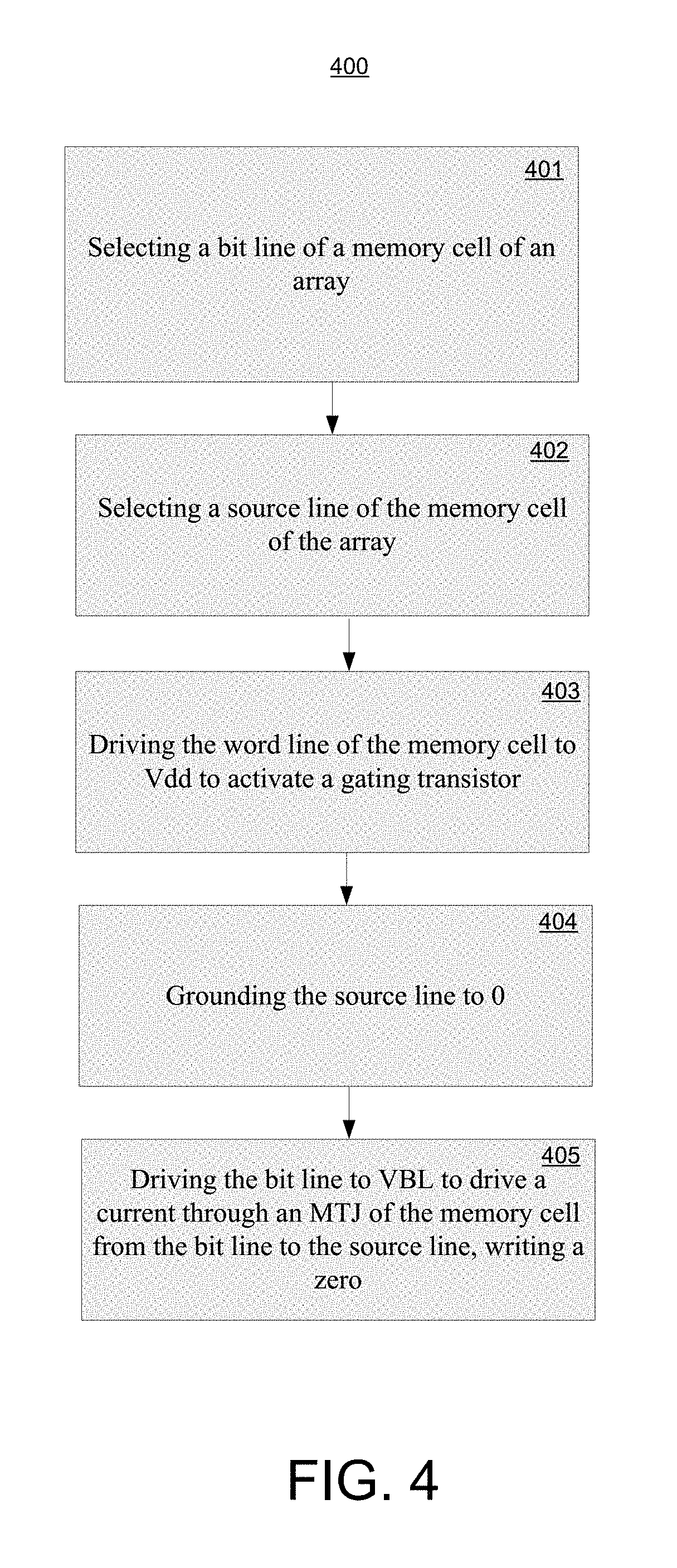
FIG. 4 shows a flow chart of the steps of a process 400 of writing a logical zero into the memory cell 300. Process 400 begins in step 401, where the bit line of the memory cell (e.g., memory cell 300) is selected. In step 402, the source line of the memory cell is selected while the remainder bit lines are allowed to float. In step 403, the word line of memory cell is driven to Vdd to activate the gating transistor. In step 404, the source line is grounded to zero. And in step 405, the bit line is driven to VBL to drive a current through the MTJ of the memory cell from the bit line to the source line, writing a logical zero.
FIG. 5 shows a flow chart of the steps of a process 500 of writing a logical one into the memory cell 300. Process 500 begins in step 501, where the bit line of the memory cell (e.g., memory cell 300) is selected, while the remainder of the bit lines are allowed to float. In step 502, the source line of the memory cell is selected. In step 503, the word line of memory cell is driven to Vdd to activate the gating transistor. In step 504, the source line is grounded to zero. And in step 505, the bit line is driven to -VBL to drive a current through the MTJ of the memory cell from the source line to the bit line, writing a logical one.
FIG. 6 shows a perpendicular memory cell 600 in accordance with one embodiment of the present invention. As shown in FIG. 6, a bit line 601 is fabricated perpendicular to a source line 602. The bit line 601 is coupled to an MTJ 605. The source line 602 is coupled to the MTJ 605 via a gating transistor 604. The gating transistor 604 is activated and deactivated by the word line 603.
The FIG. 6 second embodiment shows the bit line 601 can be driven to have a voltage at zero, and a voltage at some point between 0 and VBL, referred to in FIG. 6 as VBLmid. In this approach the source line is biased to VBLmid and the bit line alternates between 0 and VBL plus the VBLmid voltage (e.g., VBL+VBLmid to write different data values). In this implementation, 0 voltage on the bit line with VBLmid on the source line writes a logical one into the cell when the gating transistor 604 is activated. Correspondingly, VBL+VBLmid on the bit line with VBLmid on the source line writes a logical zero into the cell when the gating transistor is activated. This would reduce some of the stress on the gating transistor 604 by lessening the voltage differential between the gate and the drain.
FIG. 7 shows a flow chart of the steps of a process 700 of writing a logical zero into the memory cell 600. Process 700 begins in step 701, where the bit line of the memory cell (e.g., memory cell 600) is selected while the remainder of the bit lines are allowed to float. In step 702, the source line of the memory cell is selected. In step 703, the word line of memory cell is driven to Vdd to activate the gating transistor. In step 704, the source line is driven to VBLmid. And in step 705, the bit line is driven to VBL plus VBLmid to drive a current through the MTJ of the memory cell from the bit line to the source line, writing a logical zero.
FIG. 8 shows a flow chart of the steps of a process 800 of writing a one into the memory cell 600. Process 800 begins in step 801, where the bit line of the memory cell (e.g., memory cell 600) is selected. In step 802, the source line of the memory cell is selected. In step 803, the word line of memory cell is driven to Vdd to activate the gating transistor. In step 804, the source line is driven to VBLmid. And in step 805, the bit line is grounded to 0 to drive a current through the MTJ of the memory cell from the source line to the bit line, writing a one.
Memory Array with Horizontal Source Line and a Virtual Source Line
Embodiments of the present invention implement an MRAM array where each cell contains a perpendicular bit line to source line (e.g., horizontal source line). The source line is grouped over a number of cells and is a "virtual source line" in that it receives its voltage from all the cells of the group that are not being addressed. The word line for all cells of the group are turned on, e.g., common word line. In this third embodiment, unselected bit lines on same word line are used to advantageously bias the source line. For instance, in a first case for the cell being addressed, the bit line is driven to VBL for writing data a first data bit and the remainder of the cells of the group receive 0V on their bit lines (e.g., which "bleeds" to the source line). In a second case for the cell being addressed, the bit line is driven to 0V line for writing a second data bit and the remainder of the cells of the group receive VBL on their bit lines (e.g., which "bleeds" to the source line).
FIG. 9 shows a row 900 comprising a plurality of memory cells having a common single virtual source line in accordance with the third embodiment of the present invention. FIG. 9 shows bit lines 901-903, where bit lines 901 and 903 are unselected bit lines, and bit line 902 is a selected bit line.
In the FIG. 9 embodiment, an MRAM array is implemented where each cell contains a perpendicular bit line to source line (e.g., horizontal virtual source line). The source line (e.g., source line 950) is grouped over a number of cells and is a "virtual source line" in that it receives its voltage from the bit lines of all the cells of a group that are not being addressed. A typical group could comprise 32 bits or 64 bits. The word lines for all cells of the group are turned on, e.g., as a common word line 940. Unselected bit lines (e.g., 901 and 903) on same word line 940 are used to bias the virtual source line 950 through their associated memory cells.
In one embodiment, the word line 940 is active across the entire row. All the transistors on the row are activated. For instance, for the cell being addressed, the cell receives VBL on its bit line (e.g., 902) for writing data to MTJ 920 and the remainder of the cells of the group are grounded to receive 0V on their bit lines (e.g., 901 and 903), which "bleeds" to the source line 950. This VBL on bit line 902 causes a current to flow through the cell from the bit line 902 to the common virtual source line 950, thus writing a logical zero in the cell. The current from the unselected memory cells bleeds out onto the virtual source line 950. In the FIG. 9 embodiment, there are a large enough number of cells coupled to the virtual source line to ensure the VBL current from bit line 902 does not disturb any neighboring cells (e.g., MTJ 910 and MTJ 930).
FIG. 10 shows a row 1000 comprising a plurality of memory cells having a common single virtual source line in accordance with the third embodiment of the present invention. The FIG. 10 embodiment shows writing a one into the selected cell. As with FIG. 9, an MRAM array is implemented where each cell contains a perpendicular bit line to source line (e.g., horizontal virtual source line 1050). In order to write a one into the cell, 0V is placed on the selected bit line 1002 and VBL is driven onto the unselected bit lines (e.g., bit lines 1001 and 1003) which bleeds to the virtual source line 1050 through the unselected memory cells. This causes a current to flow through the cell from the virtual source line 1050 to the selected bit line 1002, writing a logical one.
FIG. 11 shows a flow chart of the steps of a process 1100 of writing a logical zero into the memory cell 900 of the third embodiment. Process 1100 begins in step 1101, where a common word line (e.g., word line 1040) of the memory array is driven to Vdd to activate gating transistors of the common word line. In step 1102, a bit line of the memory cell (e.g., bit line 1002) is selected. In step 1103, unselected bit lines are grounded to zero, causing 0 to bleed onto the common virtual source line as discussed above. In step 1104, the selected bit line 1002 is driven to VBL to drive a current through the MTJ of the memory cell from the selected bit line to the virtual source line, writing a logical zero.
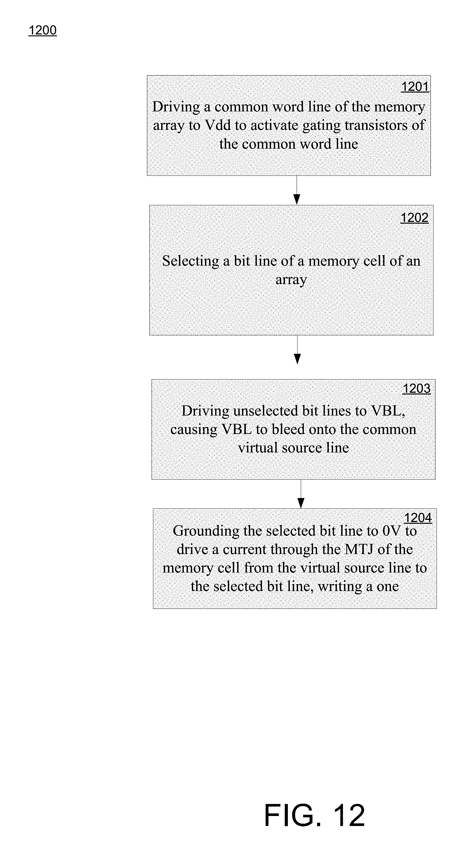
FIG. 12 shows a flow chart of the steps of a process 1200 of writing a one into the memory cell 1000 of the third embodiment. Process 1200 begins in step 1201, where a common word line (e.g., word line 1040) of the memory array is driven to Vdd to activate gating transistors of the common word line. In step 1202, a bit line of the memory cell (e.g., bit line 1002) is selected. In step 1103, unselected bit lines are driven to VBL, causing VBL to bleed onto the common virtual source line as discussed above. In step 1204, the selected bit line is grounded to drive a current through the MTJ of the memory cell from the virtual source line to the selected bit line, writing a logical one.
A Memory Array with Horizontal Source Line and Sacrificial Bitline Per Virtual Source
Embodiments of the present invention implement an MRAM array where each cell contains a perpendicular bit line to source line (e.g., horizontal source line). The source line is grouped over a number of cells and is a "virtual source line" in that it receives its voltage from a sacrificial cell. Embodiments of the present invention use a sacrificial bit line to bias the source line. For example, for the cell being addressed, that cell receives VBL for writing a first data bit (e.g., a zero) and the sacrificial cell of the common group receives 0V on its bit line (e.g., which has no memory element and directly feeds the source line). In the opposite data value case, for the cell being addressed, it receives 0V on the bit line for writing data a second data bit (e.g., a one) and the sacrificial cell of the group receives VBL on its bit line (e.g., which directly feeds to the source line). The cell can be "sacrificial" by shorting out the cell's MTJ, or by use of a fabricated via element, or by use of a fabricated direct line, etc. A number of methods are possible for shorting out the sacrificial cell. For example, in one embodiment, during post fabrication testing, bad cells can be identified and shorted out for this purpose.
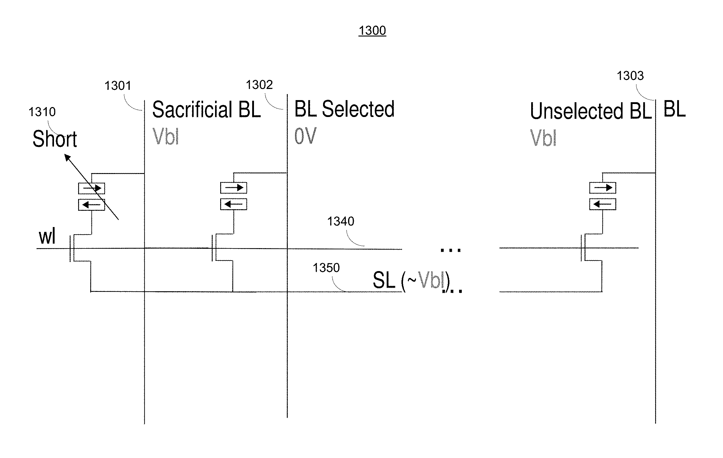
FIG. 13 shows a row 1300 comprising a plurality of memory cells having a common single virtual source line 1350 in accordance with this fourth embodiment of the present invention. FIG. 9 shows bit lines 1301-1303, where bit lines 1301 and 1303 are unselected bit lines, and bit line 1302 is a selected bit line.
In the FIG. 13 embodiment, an MRAM array is implemented where each cell contains a perpendicular bit line to source line architecture (e.g., horizontal virtual source line 1350). The source line 1350 is grouped over a number of cells and is a "virtual source line" in that it receives its voltage from all the cells of a group that are not being addressed. Additionally, FIG. 13 shows a sacrificial bit line 1301. Sacrificial bit line 1301 is connected to a "shorted out" MTJ 1310. This shorted MTJ 1310 provides a more direct path for current having low resistance from the sacrificial bit line 1301 to flow to or from the common virtual source line 1350. In one embodiment, MTJ 1310 is shorted out during post fabrication testing (e.g., by intentionally over driving the transistor). A number of methods are possible for shorting out the sacrificial cell. For example, in one embodiment, during post fabrication testing, bad cells can be identified and shorted out for this purpose. It should be noted that a sacrificial bit line can be implemented without using a virtual bit line. In one embodiment, multiple sacrificial bit lines can be implemented.
The word line for all cells of the group is turned on, e.g., as a common word line 1340. As described above, a typical group could comprise 32 bits, 64 bits. Unselected bit lines (e.g., 1301 and 1303) on same word line 1340 may be used to bias the virtual source line 1350, in conjunction with the sacrificial bit line, with the sacrificial bit line 1301 having a lower resistance connection through the shorted MTJ 1310. In one embodiment, the word line 1340 is active across the entire row. All the transistors on the row are activated. For instance, for the cell being addressed, the cell receives VBL on its bit line (e.g., 1302) for writing data and the remainder of the cells of the group may be grounded to receive 0V on their bit lines (e.g., 1301 and 1303), which "bleeds" to the source line 1350. This bleeding occurs quickly with respect to the sacrificial cell since the sacrificial bit line has a low resistance pathway provided by the shorted MTJ 1310. This VBL on bit line 1302 causes a current to flow through the cell, thus writing a logical zero in the cell. The current bleeds out onto the virtual source line 1350.
In order to write a logical one into the cell, 0V is placed on the selected bit line 1302 and VBL is driven onto the unselected bit lines (e.g., bit lines 1301 and 1303) which bleeds to the virtual source line 1350. This causes a current to flow through the cell from the virtual source line 1350 to the selected bit line 1302, writing a one.
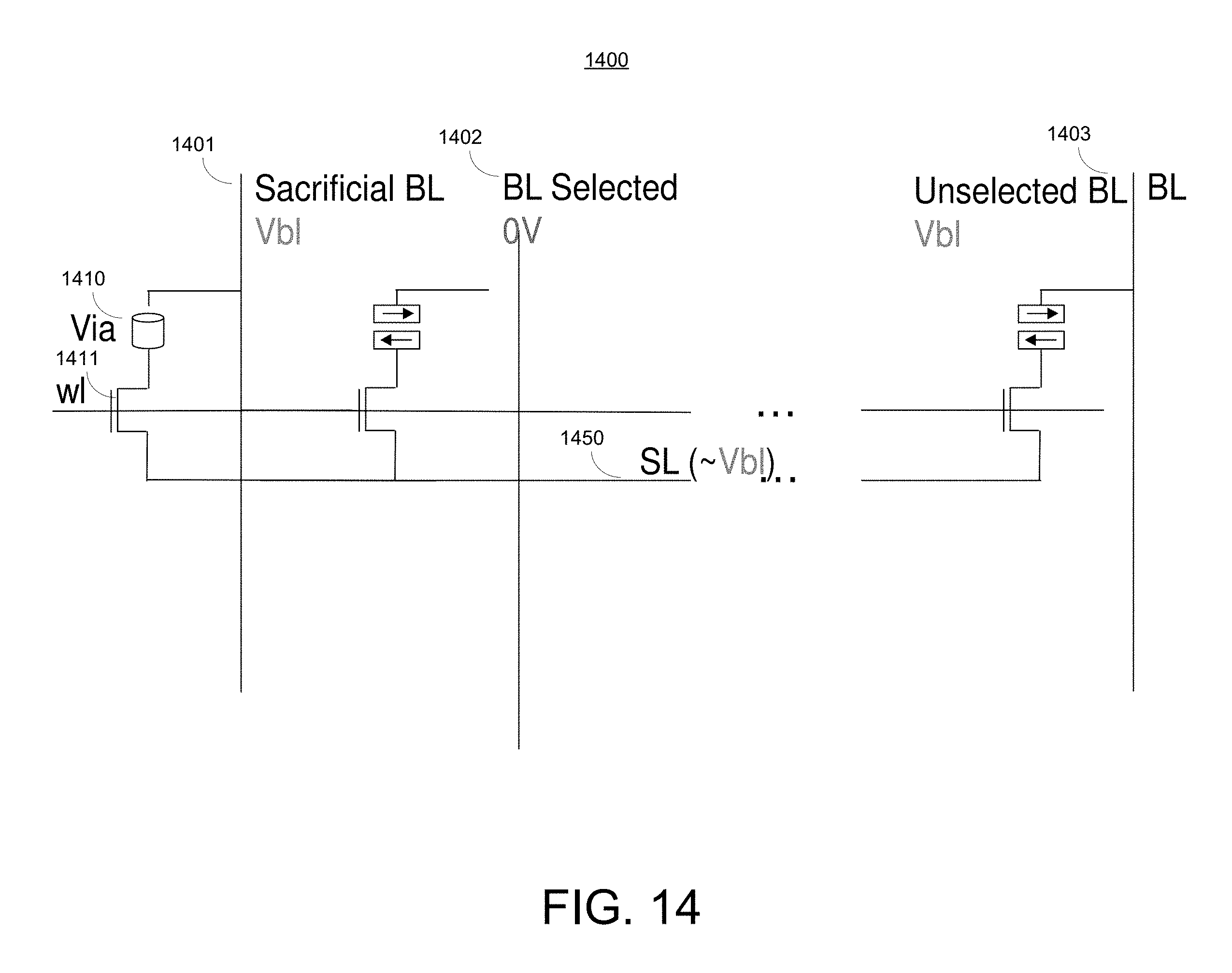
FIG. 14 shows a row 1400 comprising a plurality of memory cells having a common single virtual source line in accordance with one embodiment of the present invention. Row 1400 of FIG. 14 is substantially similar to row 1300 of FIG. 13. However, the FIG. 14 embodiment shows a via element 1410 connecting sacrificial bit line 1401 to the gating transistor 1411 and to the common virtual source line 1450. In this embodiment, the via element 1410 provides an even lower resistance pathway between the sacrificial bit line 1401 and the common virtual source line 1450 as compared to the shorted MTJ 1310. The via element is produced during die fabrication. In other aspects, the row performs the same.
FIG. 15 shows a row 1500 comprising a plurality of memory cells having a common single virtual source line in accordance with one embodiment of the present invention. Row 1500 of FIG. 15 is substantially similar to row 1400 of FIG. 14. However, the FIG. 15 embodiment shows a direct connection 1510 connecting sacrificial bit line 1501 to the common virtual source line 1550. In this embodiment, the strait through connection directly (e.g., without an intervening gating transistor) provides an even lower resistance pathway between the sacrificial bit line 1501 and the common virtual source line 1550 as compared to the shorted MTJ 1310 or the via element 1410. The direct connection is produced during die fabrication. In other aspects, the row performs the same.
FIG. 16 shows two rows of three cells each in accordance with one embodiment of the present invention. In the FIG. 16 embodiment, an MRAM array is implemented where each cell contains a perpendicular bit line to source line (e.g., horizontal virtual source line 1650). The source line 1650 is grouped over a number of cells and is a "virtual source line" in that it may receive its voltage from all the cells of a group that are not being addressed. As shown in FIG. 16, the virtual source line 1650 is able to receive voltage from both the upper row of cells and the lower row of cells, depending upon which word line is active. The upper row of cells is connected to the common word line 1640 and the lower row of cells is connected to the common word line 1645.
Additionally, FIG. 16 shows a sacrificial bit line 1601. Sacrificial bit line 1601 is connected to a "shorted out" MTJ 1610. This shorted MTJ 1610 provides a lower resistance path for current from the sacrificial bit line 1601 to flow to or from the common virtual source line 1650.
The word line for all cells of the upper row is turned on, e.g., as a common word line 1640. The common word line 1645 for the lower row of cells is unselected and turned off. This isolates the MTJs 1614-1615 from the common virtual source line 1650.
Unselected bit lines (e.g., 1601 and 1603) on same word line 1640 are used to bias the virtual source line 1650, with the sacrificial bit line 1601 having a lower resistance connection through the shorted MTJ 1610. In one embodiment, the word line 1640 is active across the entire row. All the transistors on the row are activated. For instance, for the cell being addressed, the cell receives 0 volts on its bit line (e.g., 1602) for writing data and the remainder of the cells of the group are driven to receive VBL on their bit lines (e.g., 1601 and 1603), which "bleeds" to the source line 1650. This bleeding occurs quickly since the sacrificial bit line has a low resistance pathway provided by the shorted MTJ 1610. The VBL on common virtual source line 1650 causes a current to flow through the cell to the selected bit line, thus writing a one in the cell.
In order to write a zero into the cell, VBL is placed on the selected bit line 1602 and the unselected bit lines (e.g., bit lines 1601 and 1603) are grounded which bleeds to the virtual source line 1650. This causes a current to flow through the cell from the selected bit line 1602, to the virtual source line 1650 writing a zero.
FIG. 17 shows a flow chart of the steps of a process 1700 of writing a zero into the memory cell. Process 1700 begins in step 1701, where a common word line of the memory array is driven to Vdd to activate gating transistors of the common word line. In step 1702, a bit line of the memory cell is selected. In step 1703, unselected bit lines are grounded to zero, causing 0 to bleed onto the common virtual source line via a sacrificial bit line. In one embodiment, this step is optional. This sacrificial bit line can be implemented by a shorted MTJ, a via element, or a straight through direct connection. In step 1704, the selected bit line is driven to VBL to drive a current through the MTJ of the memory cell from the selected bit line to the virtual source line, writing a zero.
FIG. 18 shows a flow chart of the steps of a process 1800 of writing a one into the memory cell. Process 1800 begins in step 1801, where a common word line of the memory array is driven to Vdd to activate gating transistors of the common word line. In step 1802, a bit line of the memory cell is selected. In step 1803, unselected bit lines are driven to VBL, causing VBL to bleed onto the common virtual source line via a sacrificial bit line. In one embodiment, this step is optional. This sacrificial bit line can be implemented by a shorted MTJ, a via element, or a straight through direct connection. In step 1804, the selected bit line is grounded to drive a current through the MTJ of the memory cell from the virtual source line to the selected bit line, writing a one.
FIG. 19 shows an exemplary portion of an MRAM array 1900 in accordance with embodiments of the present invention. FIG. 19 shows the array 1900 having an array of memory cells and having it's bit lines proceeding from top to bottom of the array and it's source lines and word lines proceeding from left to right horizontally across the array, perpendicular to the bit lines. This perpendicular architecture is featured in each of the previously discussed four embodiments of the present invention. As discussed above, the perpendicular bit line to source line arrangement provides for a smaller cell area requirement, allowing for a tighter pitch from cell to cell by elimination of the conventional dual trace line approach. This architecture avoids the trace line minimum pitch width problems of the conventional dual parallel bit line source line architecture.
The foregoing descriptions of specific embodiments of the present invention have been presented for purposes of illustration and description. They are not intended to be exhaustive or to limit the invention to the precise forms disclosed, and many modifications and variations are possible in light of the above teaching. The embodiments were chosen and described in order to best explain the principles of the invention and its practical application, to thereby enable others skilled in the art to best utilize the invention and various embodiments with various modifications as are suited to the particular use contemplated. It is intended that the scope of the invention be defined by the claims appended hereto and their equivalents.
* * * * *
D00000
D00001
D00002
D00003
D00004
D00005
D00006
D00007
D00008
D00009
D00010
D00011
D00012
D00013

D00014
D00015

D00016

D00017

D00018

D00019

XML
uspto.report is an independent third-party trademark research tool that is not affiliated, endorsed, or sponsored by the United States Patent and Trademark Office (USPTO) or any other governmental organization. The information provided by uspto.report is based on publicly available data at the time of writing and is intended for informational purposes only.
While we strive to provide accurate and up-to-date information, we do not guarantee the accuracy, completeness, reliability, or suitability of the information displayed on this site. The use of this site is at your own risk. Any reliance you place on such information is therefore strictly at your own risk.
All official trademark data, including owner information, should be verified by visiting the official USPTO website at www.uspto.gov. This site is not intended to replace professional legal advice and should not be used as a substitute for consulting with a legal professional who is knowledgeable about trademark law.