Using sub-region I/O history to cache repeatedly accessed sub-regions in a non-volatile storage device
Mathur , et al.
U.S. patent number 10,372,613 [Application Number 14/323,955] was granted by the patent office on 2019-08-06 for using sub-region i/o history to cache repeatedly accessed sub-regions in a non-volatile storage device. This patent grant is currently assigned to Sandisk Technologies LLC. The grantee listed for this patent is SanDisk Enterprise IP LLC. Invention is credited to Chayan Biswas, Baskaran Kannan, Dharani Kotte, Akshay Mathur, Sumant K. Patro.


| United States Patent | 10,372,613 |
| Mathur , et al. | August 6, 2019 |
Using sub-region I/O history to cache repeatedly accessed sub-regions in a non-volatile storage device
Abstract
Systems, methods and/or devices are used to enable using sub-region I/O history to cache repeatedly accessed sub-regions in a non-volatile storage device. In one aspect, the method includes (1) receiving a plurality of input/output (I/O) requests including read requests and write requests to be performed in a plurality of regions in a logical address space of a host, and (2) performing one or more operations for each region of the plurality of regions in the logical address space of the host, including, for each sub-region of a plurality of sub-regions of the region: (a) determining whether the sub-region is accessed more than a predetermined threshold number of times during a predetermined time period, and (b) if so, caching, from a storage medium of the storage device to a cache of the storage device, data from the sub-region.
| Inventors: | Mathur; Akshay (Los Gatos, CA), Kotte; Dharani (Fremont, CA), Biswas; Chayan (Newark, CA), Kannan; Baskaran (Round Rock, TX), Patro; Sumant K. (Fremont, CA) | ||||||||||
|---|---|---|---|---|---|---|---|---|---|---|---|
| Applicant: |
|
||||||||||
| Assignee: | Sandisk Technologies LLC
(Plano, TX) |
||||||||||
| Family ID: | 54701758 | ||||||||||
| Appl. No.: | 14/323,955 | ||||||||||
| Filed: | July 3, 2014 |
Prior Publication Data
| Document Identifier | Publication Date | |
|---|---|---|
| US 20150347013 A1 | Dec 3, 2015 | |
Related U.S. Patent Documents
| Application Number | Filing Date | Patent Number | Issue Date | ||
|---|---|---|---|---|---|
| 62005971 | May 30, 2014 | ||||
| Current U.S. Class: | 1/1 |
| Current CPC Class: | G06F 12/0871 (20130101); G06F 12/0873 (20130101); G06F 12/0862 (20130101); G06F 12/0253 (20130101); G06F 2212/6024 (20130101); G06F 2212/222 (20130101); G06F 2212/312 (20130101); G06F 2212/1044 (20130101) |
| Current International Class: | G06F 12/0873 (20160101); G06F 12/0862 (20160101); G06F 12/02 (20060101); G06F 12/0871 (20160101) |
| Field of Search: | ;711/103 |
References Cited [Referenced By]
U.S. Patent Documents
| 4173737 | November 1979 | Skerlos et al. |
| 4888750 | December 1989 | Kryder et al. |
| 4916652 | April 1990 | Schwarz et al. |
| 5129089 | July 1992 | Nielsen |
| 5270979 | December 1993 | Harari et al. |
| 5329491 | July 1994 | Brown et al. |
| 5381528 | January 1995 | Brunelle |
| 5404485 | April 1995 | Ban |
| 5488702 | January 1996 | Byers et al. |
| 5519847 | May 1996 | Fandrich et al. |
| 5530705 | June 1996 | Malone |
| 5537555 | July 1996 | Landry |
| 5551003 | August 1996 | Mattson et al. |
| 5636342 | June 1997 | Jeffries |
| 5657332 | August 1997 | Auclair et al. |
| 5666114 | September 1997 | Brodie et al. |
| 5708849 | January 1998 | Coke et al. |
| 5765185 | June 1998 | Lambrache et al. |
| 5890193 | March 1999 | Chevallier |
| 5930188 | July 1999 | Roohparvar |
| 5936884 | August 1999 | Hasbun et al. |
| 5943692 | August 1999 | Marberg et al. |
| 5946714 | August 1999 | Miyauchi |
| 5982664 | November 1999 | Watanabe |
| 6000006 | December 1999 | Bruce et al. |
| 6006345 | December 1999 | Berry, Jr. |
| 6016560 | January 2000 | Wada et al. |
| 6018304 | January 2000 | Bessios |
| 6044472 | March 2000 | Crohas |
| 6070074 | May 2000 | Perahia et al. |
| 6104304 | August 2000 | Clark et al. |
| 6119250 | September 2000 | Nishimura et al. |
| 6138261 | October 2000 | Wilcoxson et al. |
| 6182264 | January 2001 | Ott |
| 6192092 | February 2001 | Dizon et al. |
| 6260120 | July 2001 | Blumenau et al. |
| 6295592 | September 2001 | Jeddeloh et al. |
| 6311263 | October 2001 | Barlow et al. |
| 6408394 | June 2002 | Vander Kamp et al. |
| 6412042 | June 2002 | Paterson et al. |
| 6442076 | August 2002 | Roohparvar |
| 6449625 | September 2002 | Wang |
| 6484224 | November 2002 | Robins et al. |
| 6516437 | February 2003 | Van Stralen et al. |
| 6564285 | May 2003 | Mills et al. |
| 6647387 | November 2003 | McKean et al. |
| 6675258 | January 2004 | Bramhall et al. |
| 6678788 | January 2004 | O'Connell |
| 6728879 | April 2004 | Atkinson |
| 6757768 | June 2004 | Potter et al. |
| 6775792 | August 2004 | Ulrich et al. |
| 6810440 | October 2004 | Micalizzi, Jr. et al. |
| 6836808 | December 2004 | Bunce et al. |
| 6836815 | December 2004 | Purcell et al. |
| 6842436 | January 2005 | Moeller |
| 6865650 | March 2005 | Morley et al. |
| 6871257 | March 2005 | Conley et al. |
| 6895464 | May 2005 | Chow et al. |
| 6934755 | August 2005 | Saulpaugh et al. |
| 6966006 | November 2005 | Pacheco et al. |
| 6978343 | December 2005 | Ichiriu |
| 6980985 | December 2005 | Amer-Yahia et al. |
| 6981205 | December 2005 | Fukushima et al. |
| 6988171 | January 2006 | Beardsley et al. |
| 7020017 | March 2006 | Chen et al. |
| 7024514 | April 2006 | Mukaida et al. |
| 7028165 | April 2006 | Roth et al. |
| 7032123 | April 2006 | Kane et al. |
| 7043505 | May 2006 | Teague et al. |
| 7043615 | May 2006 | Kobayashi et al. |
| 7076598 | July 2006 | Wang |
| 7100002 | August 2006 | Shrader et al. |
| 7102860 | September 2006 | Wenzel |
| 7111293 | September 2006 | Hersh et al. |
| 7126873 | October 2006 | See et al. |
| 7133282 | November 2006 | Sone |
| 7155579 | December 2006 | Neils et al. |
| 7162678 | January 2007 | Saliba |
| 7173852 | February 2007 | Gorobets et al. |
| 7184446 | February 2007 | Rashid et al. |
| 7212440 | May 2007 | Gorobets |
| 7269755 | September 2007 | Moshayedi et al. |
| 7275170 | September 2007 | Suzuki |
| 7295479 | November 2007 | Yoon et al. |
| 7328377 | February 2008 | Lewis et al. |
| 7426633 | September 2008 | Thompson |
| 7486561 | February 2009 | Mokhlesi |
| 7516292 | April 2009 | Kimura et al. |
| 7523157 | April 2009 | Aguilar, Jr. et al. |
| 7527466 | May 2009 | Simmons |
| 7529466 | May 2009 | Takahashi |
| 7533214 | May 2009 | Aasheim et al. |
| 7546478 | June 2009 | Kubo et al. |
| 7566987 | July 2009 | Black et al. |
| 7571277 | August 2009 | Mizushima |
| 7574554 | August 2009 | Tanaka et al. |
| 7596643 | September 2009 | Merry et al. |
| 7669003 | February 2010 | Sinclair et al. |
| 7681106 | March 2010 | Jarrar et al. |
| 7685494 | March 2010 | Varnica et al. |
| 7707481 | April 2010 | Kirschner et al. |
| 7761655 | July 2010 | Mizushima et al. |
| 7765454 | July 2010 | Passint |
| 7774390 | August 2010 | Shin |
| 7809836 | October 2010 | Mihm et al. |
| 7840762 | November 2010 | Oh et al. |
| 7870326 | January 2011 | Shin et al. |
| 7890818 | February 2011 | Kong et al. |
| 7913022 | March 2011 | Baxter |
| 7925960 | April 2011 | Ho et al. |
| 7934052 | April 2011 | Prins et al. |
| 7945825 | May 2011 | Cohen et al. |
| 7954041 | May 2011 | Hong et al. |
| 7971112 | June 2011 | Murata |
| 7974368 | July 2011 | Shieh et al. |
| 7978516 | July 2011 | Olbrich |
| 7996642 | August 2011 | Smith |
| 8006161 | August 2011 | Lestable et al. |
| 8032724 | October 2011 | Smith |
| 8041884 | October 2011 | Chang |
| 8042011 | October 2011 | Nicolaidis et al. |
| 8069390 | November 2011 | Lin |
| 8190967 | May 2012 | Hong et al. |
| 8250380 | August 2012 | Guyot |
| 8254181 | August 2012 | Hwang et al. |
| 8259506 | September 2012 | Sommer et al. |
| 8261020 | September 2012 | Krishnaprasad et al. |
| 8312349 | November 2012 | Reche et al. |
| 8385117 | February 2013 | Sakurada et al. |
| 8412985 | April 2013 | Bowers et al. |
| 8429436 | April 2013 | Fillingim et al. |
| 8438459 | May 2013 | Cho et al. |
| 8453022 | May 2013 | Katz |
| 8473680 | June 2013 | Pruthi |
| 8510499 | August 2013 | Banerjee |
| 8531888 | September 2013 | Chilappagari et al. |
| 8554984 | October 2013 | Yano et al. |
| 8627117 | January 2014 | Johnston |
| 8634248 | January 2014 | Sprouse et al. |
| 8665650 | March 2014 | Yang |
| 8694854 | April 2014 | Dar et al. |
| 8700842 | April 2014 | Dinker |
| 8724789 | May 2014 | Altberg et al. |
| 8775741 | July 2014 | de la Iglesia |
| 8788778 | July 2014 | Boyle |
| 8832384 | September 2014 | de la Iglesia |
| 8849825 | September 2014 | McHugh et al. |
| 8874992 | October 2014 | Desireddi et al. |
| 8885434 | November 2014 | Kumar |
| 8898373 | November 2014 | Kang et al. |
| 8909894 | December 2014 | Singh et al. |
| 8910030 | December 2014 | Goel |
| 8923066 | December 2014 | Subramanian et al. |
| 8928681 | January 2015 | Edmondson et al. |
| 9002805 | April 2015 | Barber et al. |
| 9043517 | May 2015 | Sprouse et al. |
| 9052942 | June 2015 | Barber et al. |
| 9063946 | June 2015 | Barber et al. |
| 9110843 | August 2015 | Chiu et al. |
| 9128690 | September 2015 | Lotzenburger et al. |
| 9329789 | May 2016 | Chu et al. |
| 9355060 | May 2016 | Barber et al. |
| 9417917 | August 2016 | Barber et al. |
| 2001/0026949 | October 2001 | Ogawa et al. |
| 2001/0050824 | December 2001 | Buch |
| 2002/0024846 | February 2002 | Kawahara et al. |
| 2002/0032891 | March 2002 | Yada et al. |
| 2002/0036515 | March 2002 | Eldridge et al. |
| 2002/0083299 | June 2002 | Van Huben et al. |
| 2002/0099904 | July 2002 | Conley |
| 2002/0116651 | August 2002 | Beckert et al. |
| 2002/0122334 | September 2002 | Lee et al. |
| 2002/0152305 | October 2002 | Jackson et al. |
| 2002/0162075 | October 2002 | Talagala et al. |
| 2002/0165896 | November 2002 | Kim |
| 2003/0041299 | February 2003 | Kanazawa et al. |
| 2003/0043829 | March 2003 | Rashid |
| 2003/0079172 | April 2003 | Yamagishi et al. |
| 2003/0088805 | May 2003 | Majni et al. |
| 2003/0093628 | May 2003 | Matter et al. |
| 2003/0163594 | August 2003 | Aasheim et al. |
| 2003/0163629 | August 2003 | Conley et al. |
| 2003/0188045 | October 2003 | Jacobson |
| 2003/0189856 | October 2003 | Cho et al. |
| 2003/0198100 | October 2003 | Matsushita et al. |
| 2003/0204341 | October 2003 | Guliani et al. |
| 2003/0212719 | November 2003 | Yasuda et al. |
| 2003/0225961 | December 2003 | Chow et al. |
| 2004/0024957 | February 2004 | Lin et al. |
| 2004/0024963 | February 2004 | Talagala et al. |
| 2004/0057575 | March 2004 | Zhang et al. |
| 2004/0062157 | April 2004 | Kawabe |
| 2004/0073829 | April 2004 | Olarig |
| 2004/0085849 | May 2004 | Myoung et al. |
| 2004/0114265 | June 2004 | Talbert |
| 2004/0143710 | July 2004 | Walmsley |
| 2004/0148561 | July 2004 | Shen et al. |
| 2004/0153902 | August 2004 | Machado et al. |
| 2004/0158775 | August 2004 | Shibuya et al. |
| 2004/0167898 | August 2004 | Margolus et al. |
| 2004/0181734 | September 2004 | Saliba |
| 2004/0199714 | October 2004 | Estakhri et al. |
| 2004/0210706 | October 2004 | In et al. |
| 2004/0237018 | November 2004 | Riley |
| 2005/0060456 | March 2005 | Shrader et al. |
| 2005/0060501 | March 2005 | Shrader |
| 2005/0073884 | April 2005 | Gonzalez et al. |
| 2005/0108588 | May 2005 | Yuan |
| 2005/0114587 | May 2005 | Chou et al. |
| 2005/0138442 | June 2005 | Keller, Jr. et al. |
| 2005/0144358 | June 2005 | Conley et al. |
| 2005/0144361 | June 2005 | Gonzalez et al. |
| 2005/0144367 | June 2005 | Sinclair |
| 2005/0144516 | June 2005 | Gonzalez et al. |
| 2005/0154825 | July 2005 | Fair |
| 2005/0172065 | August 2005 | Keays |
| 2005/0172207 | August 2005 | Radke et al. |
| 2005/0193161 | September 2005 | Lee et al. |
| 2005/0201148 | September 2005 | Chen et al. |
| 2005/0210348 | September 2005 | Totsuka |
| 2005/0231765 | October 2005 | So et al. |
| 2005/0249013 | November 2005 | Janzen et al. |
| 2005/0251617 | November 2005 | Sinclair et al. |
| 2005/0257120 | November 2005 | Gorobets et al. |
| 2005/0273560 | December 2005 | Hulbert et al. |
| 2005/0281088 | December 2005 | Ishidoshiro et al. |
| 2005/0289314 | December 2005 | Adusumilli et al. |
| 2006/0010174 | January 2006 | Nguyen et al. |
| 2006/0039196 | February 2006 | Gorobets et al. |
| 2006/0039227 | February 2006 | Lai et al. |
| 2006/0053246 | March 2006 | Lee |
| 2006/0062054 | March 2006 | Hamilton et al. |
| 2006/0069932 | March 2006 | Oshikawa et al. |
| 2006/0085671 | April 2006 | Majni et al. |
| 2006/0087893 | April 2006 | Nishihara et al. |
| 2006/0103480 | May 2006 | Moon et al. |
| 2006/0107181 | May 2006 | Dave et al. |
| 2006/0136570 | June 2006 | Pandya |
| 2006/0136655 | June 2006 | Gorobets et al. |
| 2006/0136681 | June 2006 | Jain et al. |
| 2006/0156177 | July 2006 | Kottapalli et al. |
| 2006/0184738 | August 2006 | Bridges et al. |
| 2006/0195650 | August 2006 | Su et al. |
| 2006/0209592 | September 2006 | Li et al. |
| 2006/0224841 | October 2006 | Terai et al. |
| 2006/0244049 | November 2006 | Yaoi et al. |
| 2006/0259528 | November 2006 | Dussud et al. |
| 2006/0265568 | November 2006 | Burton |
| 2006/0291301 | December 2006 | Ziegelmayer |
| 2007/0011413 | January 2007 | Nonaka et al. |
| 2007/0033376 | February 2007 | Sinclair et al. |
| 2007/0058446 | March 2007 | Hwang et al. |
| 2007/0061597 | March 2007 | Holtzman et al. |
| 2007/0076479 | April 2007 | Kim et al. |
| 2007/0081408 | April 2007 | Kwon et al. |
| 2007/0083697 | April 2007 | Birrell et al. |
| 2007/0088716 | April 2007 | Brumme et al. |
| 2007/0091677 | April 2007 | Lasser et al. |
| 2007/0101096 | May 2007 | Gorobets |
| 2007/0106679 | May 2007 | Perrin et al. |
| 2007/0113019 | May 2007 | Beukema |
| 2007/0133312 | June 2007 | Roohparvar |
| 2007/0147113 | June 2007 | Mokhlesi et al. |
| 2007/0150790 | June 2007 | Gross et al. |
| 2007/0156842 | July 2007 | Vermeulen et al. |
| 2007/0157064 | July 2007 | Falik et al. |
| 2007/0174579 | July 2007 | Shin |
| 2007/0180188 | August 2007 | Fujbayashi et al. |
| 2007/0180346 | August 2007 | Murin |
| 2007/0191993 | August 2007 | Wyatt |
| 2007/0201274 | August 2007 | Yu et al. |
| 2007/0204128 | August 2007 | Lee et al. |
| 2007/0208901 | September 2007 | Purcell et al. |
| 2007/0234143 | October 2007 | Kim |
| 2007/0245061 | October 2007 | Harriman |
| 2007/0245099 | October 2007 | Gray et al. |
| 2007/0263442 | November 2007 | Cornwall et al. |
| 2007/0268754 | November 2007 | Lee et al. |
| 2007/0277036 | November 2007 | Chamberlain et al. |
| 2007/0279988 | December 2007 | Nguyen |
| 2007/0291556 | December 2007 | Kamei |
| 2007/0294496 | December 2007 | Goss et al. |
| 2007/0300130 | December 2007 | Gorobets |
| 2008/0013390 | January 2008 | Zipprich-Rasch |
| 2008/0019182 | January 2008 | Yanagidaira et al. |
| 2008/0022163 | January 2008 | Tanaka et al. |
| 2008/0028275 | January 2008 | Chen et al. |
| 2008/0043871 | February 2008 | Latouche et al. |
| 2008/0052446 | February 2008 | Lasser et al. |
| 2008/0052451 | February 2008 | Pua et al. |
| 2008/0056005 | March 2008 | Aritome |
| 2008/0059602 | March 2008 | Matsuda et al. |
| 2008/0071971 | March 2008 | Kim et al. |
| 2008/0077841 | March 2008 | Gonzalez et al. |
| 2008/0077937 | March 2008 | Shin et al. |
| 2008/0086677 | April 2008 | Yang et al. |
| 2008/0112226 | May 2008 | Mokhlesi |
| 2008/0141043 | June 2008 | Flynn et al. |
| 2008/0144371 | June 2008 | Yeh et al. |
| 2008/0147714 | June 2008 | Breternitz et al. |
| 2008/0147964 | June 2008 | Chow et al. |
| 2008/0147998 | June 2008 | Jeong |
| 2008/0148124 | June 2008 | Zhang et al. |
| 2008/0163030 | July 2008 | Lee |
| 2008/0168191 | July 2008 | Biran et al. |
| 2008/0168319 | July 2008 | Lee et al. |
| 2008/0170460 | July 2008 | Oh et al. |
| 2008/0180084 | July 2008 | Dougherty et al. |
| 2008/0209282 | August 2008 | Lee et al. |
| 2008/0229000 | September 2008 | Kim |
| 2008/0229003 | September 2008 | Mizushima et al. |
| 2008/0229176 | September 2008 | Arnez et al. |
| 2008/0270680 | October 2008 | Chang |
| 2008/0282128 | November 2008 | Lee et al. |
| 2008/0285351 | November 2008 | Shlick et al. |
| 2008/0313132 | December 2008 | Hao et al. |
| 2008/0320110 | December 2008 | Pathak |
| 2009/0003046 | January 2009 | Nirschl et al. |
| 2009/0003058 | January 2009 | Kang |
| 2009/0019216 | January 2009 | Yamada et al. |
| 2009/0031083 | January 2009 | Willis et al. |
| 2009/0037652 | February 2009 | Yu et al. |
| 2009/0070608 | March 2009 | Kobayashi |
| 2009/0116283 | May 2009 | Ha et al. |
| 2009/0125671 | May 2009 | Flynn et al. |
| 2009/0144598 | June 2009 | Yoon et al. |
| 2009/0158288 | June 2009 | Fulton et al. |
| 2009/0168525 | July 2009 | Olbrich et al. |
| 2009/0172258 | July 2009 | Olbrich et al. |
| 2009/0172259 | July 2009 | Prins et al. |
| 2009/0172260 | July 2009 | Olbrich et al. |
| 2009/0172261 | July 2009 | Prins et al. |
| 2009/0172262 | July 2009 | Olbrich et al. |
| 2009/0172308 | July 2009 | Prins et al. |
| 2009/0172335 | July 2009 | Kulkarni et al. |
| 2009/0172499 | July 2009 | Olbrich et al. |
| 2009/0193058 | July 2009 | Reid |
| 2009/0204823 | August 2009 | Giordano et al. |
| 2009/0207660 | August 2009 | Hwang et al. |
| 2009/0213649 | August 2009 | Takahashi et al. |
| 2009/0222708 | September 2009 | Yamaga |
| 2009/0228761 | September 2009 | Perlmutter et al. |
| 2009/0235128 | September 2009 | Eun et al. |
| 2009/0249160 | October 2009 | Gao et al. |
| 2009/0251962 | October 2009 | Yun et al. |
| 2009/0268521 | October 2009 | Ueno et al. |
| 2009/0292972 | November 2009 | Seol et al. |
| 2009/0296466 | December 2009 | Kim et al. |
| 2009/0296486 | December 2009 | Kim et al. |
| 2009/0310422 | December 2009 | Edahiro et al. |
| 2009/0319864 | December 2009 | Shrader |
| 2010/0002506 | January 2010 | Cho et al. |
| 2010/0008175 | January 2010 | Sweere et al. |
| 2010/0011261 | January 2010 | Cagno et al. |
| 2010/0020620 | January 2010 | Kim et al. |
| 2010/0037012 | February 2010 | Yano et al. |
| 2010/0054034 | March 2010 | Furuta et al. |
| 2010/0061151 | March 2010 | Miwa et al. |
| 2010/0091535 | April 2010 | Sommer et al. |
| 2010/0103737 | April 2010 | Park |
| 2010/0110798 | May 2010 | Hoei et al. |
| 2010/0115206 | May 2010 | de la Iglesia |
| 2010/0118608 | May 2010 | Song et al. |
| 2010/0138592 | June 2010 | Cheon |
| 2010/0153616 | June 2010 | Garratt |
| 2010/0161936 | June 2010 | Royer et al. |
| 2010/0174959 | July 2010 | No et al. |
| 2010/0185807 | July 2010 | Meng et al. |
| 2010/0199027 | August 2010 | Pucheral et al. |
| 2010/0199125 | August 2010 | Reche |
| 2010/0199138 | August 2010 | Rho |
| 2010/0202196 | August 2010 | Lee et al. |
| 2010/0202239 | August 2010 | Moshayedi et al. |
| 2010/0208521 | August 2010 | Kim et al. |
| 2010/0257379 | October 2010 | Wang et al. |
| 2010/0262889 | October 2010 | Bains |
| 2010/0281207 | November 2010 | Miller et al. |
| 2010/0281342 | November 2010 | Chang et al. |
| 2010/0306222 | December 2010 | Freedman et al. |
| 2010/0332858 | December 2010 | Trantham et al. |
| 2010/0332863 | December 2010 | Johnston |
| 2011/0010514 | January 2011 | Benhase et al. |
| 2011/0022779 | January 2011 | Lund et al. |
| 2011/0022819 | January 2011 | Post et al. |
| 2011/0051513 | March 2011 | Shen et al. |
| 2011/0066597 | March 2011 | Mashtizadeh et al. |
| 2011/0066806 | March 2011 | Chhugani et al. |
| 2011/0072207 | March 2011 | Jin et al. |
| 2011/0072302 | March 2011 | Sartore |
| 2011/0078407 | March 2011 | Lewis |
| 2011/0078496 | March 2011 | Jeddeloh |
| 2011/0083060 | April 2011 | Sakurada et al. |
| 2011/0099460 | April 2011 | Dusija et al. |
| 2011/0113281 | May 2011 | Zhang et al. |
| 2011/0122691 | May 2011 | Sprouse |
| 2011/0131444 | June 2011 | Buch et al. |
| 2011/0138260 | June 2011 | Savin |
| 2011/0173378 | July 2011 | Filor et al. |
| 2011/0179249 | July 2011 | Hsiao |
| 2011/0199825 | August 2011 | Han et al. |
| 2011/0205823 | August 2011 | Hemink et al. |
| 2011/0213920 | September 2011 | Frost et al. |
| 2011/0222342 | September 2011 | Yoon et al. |
| 2011/0225346 | September 2011 | Goss et al. |
| 2011/0225347 | September 2011 | Goss et al. |
| 2011/0228601 | September 2011 | Olbrich et al. |
| 2011/0231600 | September 2011 | Tanaka et al. |
| 2011/0239077 | September 2011 | Bai et al. |
| 2011/0264843 | October 2011 | Haines et al. |
| 2011/0271040 | November 2011 | Kamizono |
| 2011/0283119 | November 2011 | Szu et al. |
| 2011/0289125 | November 2011 | Guthery |
| 2011/0320733 | December 2011 | Sanford et al. |
| 2012/0011393 | January 2012 | Roberts et al. |
| 2012/0017053 | January 2012 | Yang et al. |
| 2012/0023144 | January 2012 | Rub |
| 2012/0026799 | February 2012 | Lee |
| 2012/0054414 | March 2012 | Tsai et al. |
| 2012/0063234 | March 2012 | Shiga et al. |
| 2012/0072639 | March 2012 | Goss et al. |
| 2012/0096217 | April 2012 | Son et al. |
| 2012/0110250 | May 2012 | Sabbag et al. |
| 2012/0117317 | May 2012 | Sheffler |
| 2012/0117397 | May 2012 | Kolvick et al. |
| 2012/0124273 | May 2012 | Goss et al. |
| 2012/0131286 | May 2012 | Faith et al. |
| 2012/0151124 | June 2012 | Baek et al. |
| 2012/0151253 | June 2012 | Horn |
| 2012/0151294 | June 2012 | Yoo et al. |
| 2012/0173797 | July 2012 | Shen |
| 2012/0173826 | July 2012 | Takaku |
| 2012/0185750 | July 2012 | Hayami |
| 2012/0195126 | August 2012 | Roohparvar |
| 2012/0203804 | August 2012 | Burka et al. |
| 2012/0203951 | August 2012 | Wood et al. |
| 2012/0210095 | August 2012 | Nellans et al. |
| 2012/0216079 | August 2012 | Fai et al. |
| 2012/0233391 | September 2012 | Frost et al. |
| 2012/0236658 | September 2012 | Byom et al. |
| 2012/0239858 | September 2012 | Melik-Martirosian |
| 2012/0239868 | September 2012 | Ryan et al. |
| 2012/0239976 | September 2012 | Cometti et al. |
| 2012/0246204 | September 2012 | Nalla et al. |
| 2012/0259863 | October 2012 | Bodwin et al. |
| 2012/0275466 | November 2012 | Bhadra et al. |
| 2012/0278564 | November 2012 | Goss et al. |
| 2012/0284574 | November 2012 | Avila et al. |
| 2012/0284587 | November 2012 | Yu et al. |
| 2012/0297122 | November 2012 | Gorobets |
| 2013/0007073 | January 2013 | Varma |
| 2013/0007343 | January 2013 | Rub et al. |
| 2013/0007381 | January 2013 | Palmer |
| 2013/0007543 | January 2013 | Goss et al. |
| 2013/0024735 | January 2013 | Chung et al. |
| 2013/0031438 | January 2013 | Hu et al. |
| 2013/0036418 | February 2013 | Yadappanavar et al. |
| 2013/0038380 | February 2013 | Cordero et al. |
| 2013/0047045 | February 2013 | Hu et al. |
| 2013/0058145 | March 2013 | Yu et al. |
| 2013/0070527 | March 2013 | Sabbag et al. |
| 2013/0073784 | March 2013 | Ng et al. |
| 2013/0073798 | March 2013 | Kang et al. |
| 2013/0073924 | March 2013 | D'Abreu et al. |
| 2013/0079942 | March 2013 | Smola et al. |
| 2013/0086131 | April 2013 | Hunt et al. |
| 2013/0086132 | April 2013 | Hunt et al. |
| 2013/0094288 | April 2013 | Patapoutian et al. |
| 2013/0103978 | April 2013 | Akutsu |
| 2013/0110891 | May 2013 | Ogasawara et al. |
| 2013/0111279 | May 2013 | Jeon et al. |
| 2013/0111298 | May 2013 | Seroff et al. |
| 2013/0117606 | May 2013 | Anholt et al. |
| 2013/0121084 | May 2013 | Jeon et al. |
| 2013/0124792 | May 2013 | Melik-Martirosian et al. |
| 2013/0124888 | May 2013 | Tanaka et al. |
| 2013/0128666 | May 2013 | Avila et al. |
| 2013/0132647 | May 2013 | Melik-Martirosian |
| 2013/0132652 | May 2013 | Wood et al. |
| 2013/0159609 | June 2013 | Haas et al. |
| 2013/0166824 | June 2013 | Shim et al. |
| 2013/0176784 | July 2013 | Cometti et al. |
| 2013/0179646 | July 2013 | Okubo et al. |
| 2013/0191601 | July 2013 | Peterson et al. |
| 2013/0194865 | August 2013 | Bandic et al. |
| 2013/0194874 | August 2013 | Mu et al. |
| 2013/0232289 | September 2013 | Zhong et al. |
| 2013/0238576 | September 2013 | Binkert et al. |
| 2013/0254498 | September 2013 | Adachi et al. |
| 2013/0254507 | September 2013 | Islam et al. |
| 2013/0258738 | October 2013 | Barkon et al. |
| 2013/0265838 | October 2013 | Li |
| 2013/0282955 | October 2013 | Parker et al. |
| 2013/0290611 | October 2013 | Biederman et al. |
| 2013/0297613 | November 2013 | Yu |
| 2013/0301373 | November 2013 | Tam |
| 2013/0304980 | November 2013 | Nachimuthu et al. |
| 2013/0314988 | November 2013 | Desireddi et al. |
| 2013/0343131 | December 2013 | Wu et al. |
| 2013/0346672 | December 2013 | Sengupta et al. |
| 2014/0013027 | January 2014 | Jannyavula Venkata et al. |
| 2014/0013188 | January 2014 | Wu et al. |
| 2014/0025864 | January 2014 | Zhang et al. |
| 2014/0032890 | January 2014 | Lee et al. |
| 2014/0063905 | March 2014 | Ahn et al. |
| 2014/0067761 | March 2014 | Chakrabarti et al. |
| 2014/0071761 | March 2014 | Sharon et al. |
| 2014/0075133 | March 2014 | Li et al. |
| 2014/0082261 | March 2014 | Cohen et al. |
| 2014/0082310 | March 2014 | Nakajima |
| 2014/0082456 | March 2014 | Li et al. |
| 2014/0082459 | March 2014 | Li et al. |
| 2014/0095775 | April 2014 | Talagala et al. |
| 2014/0101389 | April 2014 | Nellans et al. |
| 2014/0115238 | April 2014 | Xi et al. |
| 2014/0122818 | May 2014 | Hayasaka et al. |
| 2014/0122907 | May 2014 | Johnston |
| 2014/0136762 | May 2014 | Li et al. |
| 2014/0136883 | May 2014 | Cohen |
| 2014/0136927 | May 2014 | Li et al. |
| 2014/0143505 | May 2014 | Sim et al. |
| 2014/0153333 | June 2014 | Avila et al. |
| 2014/0157065 | June 2014 | Ong |
| 2014/0173224 | June 2014 | Fleischer et al. |
| 2014/0181458 | June 2014 | Loh |
| 2014/0201596 | July 2014 | Baum et al. |
| 2014/0223084 | August 2014 | Lee et al. |
| 2014/0244578 | August 2014 | Winkelstraeter |
| 2014/0258755 | September 2014 | Stenfort |
| 2014/0269090 | September 2014 | Flynn et al. |
| 2014/0279909 | September 2014 | Sudarsanam et al. |
| 2014/0310494 | October 2014 | Higgins et al. |
| 2014/0359044 | December 2014 | Davis et al. |
| 2014/0359381 | December 2014 | Takeuchi et al. |
| 2015/0023097 | January 2015 | Khoueir et al. |
| 2015/0032967 | January 2015 | Udayashankar et al. |
| 2015/0037624 | February 2015 | Thompson et al. |
| 2015/0153799 | June 2015 | Lucas et al. |
| 2015/0153802 | June 2015 | Lucas et al. |
| 2015/0212943 | July 2015 | Yang |
| 2015/0268879 | September 2015 | Chu |
| 2015/0286438 | October 2015 | Simionescu et al. |
| 1 299 800 | Apr 2003 | EP | |||
| 1 465 203 | Oct 2004 | EP | |||
| 1 990 921 | Nov 2008 | EP | |||
| 2 386 958 | Nov 2011 | EP | |||
| 2 620 946 | Jul 2013 | EP | |||
| 2002-532806 | Oct 2002 | JP | |||
| WO 2007/036834 | Apr 2007 | WO | |||
| WO 2007/080586 | Jul 2007 | WO | |||
| WO 2008/075292 | Jun 2008 | WO | |||
| WO 2008/121553 | Oct 2008 | WO | |||
| WO 2008/121577 | Oct 2008 | WO | |||
| WO 2009/028281 | Mar 2009 | WO | |||
| WO 2009/032945 | Mar 2009 | WO | |||
| WO 2009/058140 | May 2009 | WO | |||
| WO 2009/084724 | Jul 2009 | WO | |||
| WO 2009/134576 | Nov 2009 | WO | |||
| WO 2011/024015 | Mar 2011 | WO | |||
Other References
|
Barr, "Introduction to Watchdog Timers," Oct. 2001, 3 pgs. cited by applicant . Canim, "Buffered Bloom Filters on Solid State Storage," ADMS*10. Singapore, Sep. 13-17, 2010, 8 pgs. cited by applicant . Kang, "A Multi-Channel Architecture for High-Performance NAND Flash-Based Storage System," J. Syst. Archit., vol. 53, Issue 9, Sep. 2007, 15 pgs. cited by applicant . Kim, "A Space-Efficient Flash Translation Layer for CompactFlash Systems," May 2002, IEEE vol. 48, No. 2, 10 pgs. cited by applicant . Lu, "A Forest-structured Bloom Filter with Flash Memory," MSST 2011, Denver, CO, May 23-27, 2011, article, 6 pgs. cited by applicant . Lu, "A Forest-structured Bloom Filter with Flash Memory," MSST 2011, Denver, CO, May 23-27, 2011, presentation slides, 25 pgs. cited by applicant . McLean, "Information Technology--AT Attachment with Packet Interface Extension," Aug. 19, 1998, 339 pgs. cited by applicant . Microchip Technology, "Section 10. Watchdog Timer and Power-Saving Modes," 2005. 14 pages. cited by applicant . Park et al., "A High Perfomance Controller for NAND Flash-Based Solid State Disk (NSSD)," Proceedings of Non-Volatile Semiconductor Memory Workshop, Feb. 2006. 4 pgs. cited by applicant . Zeidman, "Verilog Designer's Library," 1999, 9 pgs. cited by applicant . International Search Report and Written Opinion dated Jun. 6, 2013, received in International Patent Application No. PCT/US2012/059447, which corresponds to U.S. Appl. No. 13/602,031, 12 pgs (Tai). cited by applicant . International Search Report and Written Opinion dated May 23, 2013, received in International Patent Application No. PCT/US2012/065914, which corresponds to U.S. Appl. No. 13/679,963, 7 pgs (Frayer). cited by applicant . International Search Report and Written Opinion, dated Mar. 19, 2009 received in International Patent Application No. PCT/US08/88133, which corresponds to U.S. Appl. No. 12/082,202, 7 pgs (Prins). cited by applicant . International Search Report and Written Opinion dated Feb. 19, 2009. received in International Patent Application No. PCT/US08/88236, which corresponds to U.S. Appl. No. 12/082,203, 7 pgs (Olbrich). cited by applicant . International Search Report and Written Opinion dated Feb. 19, 2009. received in International Patent Application No. PCT/US08/88217, which corresponds to U.S. Appl. No. 12/082,204, 7 pgs (Olbrich). cited by applicant . International Search Report and Written Opinion, dated Mar. 19, 2009, received in International Patent Application No. PCT/US08/88136, which corresponds to U.S. Appl. No. 12/082,205, 7 pgs (Olbrich). cited by applicant . International Search Report and Written Opinion dated Feb. 18, 2009, received in International Patent Application No. PCT/US08/88206, which corresponds to U.S. Appl. No. 12/082,206, 7 pgs (Prins). cited by applicant . International Search Report and Written Opinion dated Feb. 27, 2009, received in International Patent Application No. PCT/US2008/088154, which corresponds to U.S. Appl. No. 12/082,207, 8 pgs (Prins). cited by applicant . European Search Report dated Feb. 23, 2012, received in European Patent Application No. 08866997.3, which corresponds to U.S. Appl. No. 12/082,207, 6 pgs (Prins). cited by applicant . Office Action dated Apr. 18, 2012, received in Chinese Patent Application No. 200880127623.8, which corresponds to US. Appl. No. 12/082,207, 12 pgs (Prins). cited by applicant . Office Action dated Dec. 31, 2012, received in Chinese Patent Application 20080127623.8, which corresponds to U.S. Appl. No. 12/082,207, 9 pgs (Prins). cited by applicant . Notification of the Decision to Grant a Patent Right for Patent for Invention dated Jul. 4, 2013, received in Chinese Patent Application No. 200880127623.8, which corresponds U.S. Appl. No. 12/082,207, 1 pg (Prins). cited by applicant . Office Action dated Jul. 24, 2012, received in Japanese Patent Application No. JP 2010-540863, 3 pgs (Prins). cited by applicant . International Search Report and Written Opinion dated Feb. 13, 2009, received in International Patent Application No. PCT/US08/88164, which corresponds to U.S. Appl. No. 12/082,220, 6 pgs (Olbrich). cited by applicant . International Search Report and Written Opinion dated Feb. 26, 2009, received in International Patent Application No. PCT/US08/88146, which corresponds to U.S. Appl. No. 12/082,221, 10 pgs (Prins). cited by applicant . International Search Report and Written Opinion dated Feb. 19, 2009, received in International Patent Application No. PCT/US08/88232, which corresponds to U.S. Appl. No. 12/082,222, 8 pgs (Olbrich). cited by applicant . International Search Report and Written Opinion dated Feb. 13, 2009, received in International Patent Application No. PCT/US08/88229, which corresponds to U.S. Appl. No. 12/082,223, 7 pgs (Olbrich). cited by applicant . International Search Report and Written Opinion dated Oct. 27, 2011, received in International Patent Application No. PCT/US2011/028637, which corresponds to U.S. Appl. No. 12/726,200, 13 pgs (Olbrich). cited by applicant . International Search Report and Written Opinion dated Aug. 31, 2012, received in International Patent Application No. PCT/US2012/042764, which corresponds to U.S. Appl. No. 13/285,873, 12 pgs (Frayer). cited by applicant . International Search Report and Written Opinion dated Mar. 4, 2013, received in PCT/US2012/042771, which corresponds to U.S. Appl. No. 13/286,012, 14 pgs (Stonelake). cited by applicant . International Search Report and Written Opinion dated Sep. 26, 2012, received in International Patent Application No. PCT/US2012/042775, which corresponds to U.S. Appl. No. 13/285,892, 8 pgs (Weston-Lewis et al.). cited by applicant . International Search Report and Written Opinion dated Jun. 6, 2013, received in International Patent Application No. PCT/US2012/059453, which corresponds to U.S. Appl. No. 13/602,039, 12 pgs (Frayer). cited by applicant . International Search Report and Written Opinion dated Feb. 14, 2013, received in International Patent Application No. PCT/US2012/059459, which corresponds to U.S. Appl. No. 13/602,047, 9 pgs (Tai). cited by applicant . International Search Report and Written Opinion dated Mar. 7, 2014, received in International Patent Application No. PCT/US2013/074772, which corresponds to U.S. Appl. No. 13/831,218, 10 pages (George). cited by applicant . International Search Report and Written Opinion dated Mar. 24, 2014, received in International Patent Application No. PCT/US2013/074777, which corresponds to U.S. Appl. No. 13/831,308, 10 pages (George). cited by applicant . International Search Report and Written Opinion dated Mar. 7, 2014, received in International Patent Application No. PCT/US2013/074779, which corresponds to U.S. Appl. No. 13/831,374, 8 pages (George). cited by applicant . International Search Report and Written Opinion dated Apr. 5, 2013, received in International Patent Application No. PCT/US2012/065916, which corresponds to U.S. Appl. No. 13/679,969, 7 pgs (Frayer). cited by applicant . International Search Report and Written Opinion dated Jun. 17, 2013, received in International Patent Application No. PCT/US2012/065919, which corresponds to U.S. Appl. No. 13/679,970, 8 pages (Frayer). cited by applicant . International Search Report and Written Opinion dated Jul. 25, 2014, received in International Patent Application No. PCT/US2014/029453, which corresponds to U.S. Appl. No. 13/963,444, 9 pages (Frayer). cited by applicant . Bayer, "Prefix B-Trees", ip.com Journal, ip.com Inc., West Henrietta, NY, Mar. 30, 2007, 29 pages. cited by applicant . Bhattacharjee et al., "Efficient Index Compression in DB2 LUW", IBM Research Report, Jun. 23, 2009, http://domino.research.ibm.com/library/cyberdig.nsf/papers/40B2C45876D0D7- 47852575E100620CE7/$File/rc24815.pdf, 13 pages. cited by applicant . Lee et al., "A Semi-Preemptive Garbage Collector for Solid State Drives," Apr. 2011, IEEE, pp. 12-21. cited by applicant . Oracle, "Oracle9i: Database Concepts", Jul. 2001, http://docs.oracle.com/cd/A91202_01/901_doc/server.901/a88856.pdf, 49 pages. cited by applicant . Office Action dated Feb. 17, 2015, received in Chinese Patent Application No. 201210334987.1, which corresponds to U.S. Appl. No. 12/082,207, 9 pages (Prins). cited by applicant . International Search Report and Written Opinion dated May 4, 2015, received in International Patent Application No. PCT/US2014/065987, which corresponds to U.S. Appl. No. 14/135,400, 12 pages (George). cited by applicant . International Search Report and Written Opinion dated Mar. 17, 2015, received in International Patent Application No. PCT/US2014/067467, which corresponds to U.S. Appl. No. 14/135,420, 13 pages (Lucas). cited by applicant . International Search Report and Written Opinion dated Apr. 20, 2015, received in International Patent Application No. PCT/US2014/063949, which corresponds to U.S. Appl. No. 14/135,433, 21 pages (Delpapa). cited by applicant . International Search Report and Written Opinion dated Jun. 8, 2015, received in International Patent Application No. PCT/US2015/018252, which corresponds to U.S. Appl. No. 14/339,072, 9 pages (Busch). cited by applicant . International Search Report and Written Opinion dated Jun. 2, 2015, received in International Patent Application No. PCT/US2015/018255, which corresponds to U.S. Appl. No. 14/336,967, 14 pages (Chander). cited by applicant . IBM Research-Zurich, "The Fundamental Limit of Flash Random Write Performance: Understanding, Analysis and Performance Modeling," Mar. 31, 2010, pp. 1-15. cited by applicant . Office Action dated Dec. 8, 2014, received in Chinese Patent Application No. 201180021660.2, which corresponds to U.S. Appl. No. 12/726,200, 7 pages (Olbrich). cited by applicant . Office Action dated Jul. 31, 2015, received in Chinese Patent Application No. 201180021660.2, which corresponds to U.S. Appl. No. 12/726,200, 9 pages (Olbrich). cited by applicant . International Search Report and Written Opinion dated Jun. 30, 2015, received in International Patent Application No. PCT/US2015/023927, which corresponds to U.S. Appl. No. 14/454,687, 11 pages (Kadayam). cited by applicant . International Search Report and Written Opinion dated Jul. 23, 2015, received in International Patent Application No. PCT/US2015/030850, which corresponds to U.S. Appl. No. 14/298,843, 12 pages (Ellis). cited by applicant . International Search Report and Written Opinion dated Sep. 14, 2015, received in International Patent Application No. PCT/US2015/036807, which corresponds to U.S. Appl. No. 14/311,152, 9 pages (Higgins). cited by applicant . Ashkenazi et al., "Platform independent overall security architecture in muiti-processor system-on-chip integrated circuits for use in mobile phones and handheld devices," ScienceDirect, Computers and Electrical Engineering 33 (2007), 18 pages. cited by applicant . Invitation to Pay Additional Fees dated Feb. 13, 2015, received in International Patent Application No. PCT/US2014/063949, which corresponds to U.S. Appl. No. 14/135,433, 6 pages (Delpapa). cited by applicant . International Search Report and Written Opinion dated Mar. 9, 2015, received in International Patent Application No. PCT/US2014/059747, which corresponds to U.S. Appl. No. 14/137,440, 9 pages (Fitzpatrick). cited by applicant . International Search Report and Written Opinion dated Jan. 21, 2015, received in International Application No. PCT/US2014/059748, which corresponds to U.S. Appl. No. 14/137,511, 13 pages (Dancho). cited by applicant . International Search Report and Written Opinion dated Feb. 18, 2015, received in International Application No. PCT/US2014/066921, which corresponds to U.S. Appl. No. 14/135,260, 13 pages (Fitzpatrick). cited by applicant . Oestreicher et al., "Object Lifetimes in Java Card," 1999, USENIX, 10 pages. cited by applicant . Office Action dated Apr. 25, 2016, received in Chinese Patent Application No. 201280066282.4, which corresponds to U.S. Appl. No. 13/602,047, 8 pages (Tai). cited by applicant . International Preliminary Report on Patentability dated May 24, 2016, received in International Patent Application No. PCT/US2014/065987, which corresponds to U.S. Appl. No. 14/135,400, 9 pages (George). cited by applicant . Office Action dated Jan. 11, 2017, received in Chinese Patent Application No. 201280066282.4, which corresponds to U.S. Appl. No. 13/602,047, 3 pages (Tai). cited by applicant . Gasior, "Gigabyte's i-Ram storage device, Ram disk without the fuss," The Tech Report, p. 1, Jan. 25, 2006, 5 pages. cited by applicant . Office Action dated May 3, 2017, received in Chinese Patent Application No. 201480015991.9, which corresponds to U.S. Appl. No. 13/963,444, 2 pages (Frayer). cited by applicant . International Preliminary Report on Patentability dated Dec. 6, 2016, received in International Patent Application No. PCT/US2015/030850, which corresponds to U.S. Appl. No. 14/298,843, 8 pages (Ellis). cited by applicant . International Preliminary Report on Patentability dated Dec. 20, 2016, received in International Patent Application No. PCT/US2015/036807, which corresponds to U.S. Appl. No. 14/311,152, 6 pages (Higgins). cited by applicant. |
Primary Examiner: Sain; Gautam
Attorney, Agent or Firm: Morgan, Lewis & Bockius LLP
Parent Case Text
RELATED APPLICATION
This application claims priority to U.S. Provisional Patent Application Ser. No. 62/005,971, filed May 30, 2014, entitled "Using Sub-Region I/O History to Cache Repeatedly Accessed Sub-Regions in a Non-Volatile Storage Device," which is hereby incorporated by reference in its entirety.
Claims
What is claimed is:
1. A method, comprising: receiving, at a storage device, a plurality of input/output (I/O) requests from a host, the plurality of I/O requests including read requests and write requests to be performed in a plurality of regions in a logical address space of the host; and performing one or more operations for each region of the plurality of regions in the logical address space of the host, including: for each sub-region of a plurality of sub-regions of the region in the logical address space of the host, wherein each sub-region includes two or more pages and two or more logical block addresses (LBAs): determining, and storing in a data structure in the storage device, a total number of times the sub-region in the logical address space of the host is accessed during a predetermined time period; in accordance with the determined total number of times the sub-region is accessed, determining whether the sub-region in the logical address space of the host is accessed more than a predetermined threshold number of times during the predetermined time period; and in accordance with a determination that the sub-region in the logical address space of the host is accessed more than the predetermined threshold number of times in the predetermined time period, caching, from a storage medium of the storage device to a cache of the storage device, data from the sub-region.
2. The method of claim 1, wherein, with respect to a sub-region of the plurality of sub-regions, caching data from the sub-region includes: in response to a subsequent write request to the sub-region, caching the sub-region, wherein the subsequent write request to the sub-region is received subsequent to the determination that the sub-region in the logical address space of the host is accessed more than the predetermined threshold number of times in the predetermined time period.
3. The method of claim 1, further comprising, with respect to a sub-region of the plurality of sub-regions, subsequent to caching data from the sub-region: writing subsequent write requests to the sub-region to the cache; reading subsequent read requests from the sub-region from the cache; and writing contents of the cache to the storage medium of the storage device in a merged operation.
4. The method of claim 1, further comprising, for each region of the plurality of regions in the logical address space, storing information in a data structure to maintain a history of I/O request patterns in the region for the predetermined time period.
5. The method of claim 1, wherein the predetermined time period is configurable.
6. The method of claim 1, wherein the predetermined threshold number is configurable.
7. The method of claim 1, wherein the storage device comprises one or more flash memory devices.
8. The method of claim 1, wherein the storage device comprises one or more three-dimensional (3D) memory devices and circuitry associated with operation of memory elements in the one or more 3D memory devices.
9. The method of claim 1, wherein the plurality of regions in the logical address space of the host are fixed-size, predefined regions in the logical address space of the host, and the plurality of sub-regions of each region of the plurality of regions in the logical address space of the host are fixed-size, predefined sub-regions in the logical address space of the host, and the fixed-size of the sub-regions is smaller than the fixed-size of the regions in the logical address space of the host.
10. The method of claim 1, including translating a respective logical address, in the logical address space of the host, to a corresponding physical address in a physical address space of the storage device.
11. The method of claim 1, wherein performing one or more operations for each region of the plurality of regions in the logical address space of the host includes: for each sub-region of the plurality of sub-regions of the region in the logical address space of the host, maintaining an access count for the sub-region in the logical address space of the host.
12. The method of claim 11, wherein determining whether the sub-region in the logical address space of the host is accessed more than the predetermined threshold number of times during the predetermined time period includes determining, in accordance with the access count, whether the sub-region in the logical address space of the host is accessed more than the predetermined threshold number of times during the predetermined time period.
13. A storage device, comprising: one or more processors; and memory storing one or more programs, which when executed by the one or more processors cause the storage device to: receive, at the storage device, a plurality of input/output (I/O) requests from a host, the plurality of I/O requests including read requests and write requests to be performed in a plurality of regions in a logical address space of the host; and perform one or more operations for each region of the plurality of regions in the logical address space of the host, including: for each sub-region of a plurality of sub-regions of the region in the logical address space of the host, wherein each sub-region includes two or more pages and two or more logical block addresses (LBAs): determining, and storing in a data structure in the storage device, a total number of times the sub-region in the logical address space of the host is accessed during a predetermined time period; in accordance with the determined total number of times the sub-region is accessed, determining whether the sub-region in the logical address space of the host is accessed more than a predetermined threshold number of times during the predetermined time period; and in accordance with the determination that the sub-region in the logical address space of the host is accessed more than the predetermined threshold number of times in the predetermined time period, caching, from a storage medium of the storage device to a cache of the storage device, data from the sub-region.
14. The storage device of claim 13, wherein, with respect to a sub-region of the plurality of sub-regions, caching data from the sub-region includes: in response to a subsequent write request to the sub-region, caching the sub-region, wherein the subsequent write request to the sub-region is received subsequent to the determination that the sub-region in the logical address space of the host is accessed more than the predetermined threshold number of times in the predetermined time period.
15. The storage device of claim 13, wherein the one or more programs, which when executed by the one or more processors, further cause the storage device to, with respect to a sub-region of the plurality of sub-regions, subsequent to caching data from the sub-region: write subsequent write requests to the sub-region to the cache; read subsequent read requests from the sub-region from the cache; and write contents of the cache to the storage medium of the storage device in a merged operation.
16. The storage device of claim 13, wherein the one or more programs, which when executed by the one or more processors, further cause the storage device to: for each region of the plurality of regions in the logical address space, store information in a data structure to maintain a history of I/O request patterns in the region for the predetermined time period.
17. The storage device of claim 13, wherein the plurality of regions in the logical address space of the host are fixed-size, predefined regions in the logical address space of the host, and the plurality of sub-regions of each region of the plurality of regions in the logical address space of the host are fixed-size, predefined sub-regions in the logical address space of the host, and the fixed-size of the sub-regions is smaller than the fixed-size of the regions in the logical address space of the host.
18. A storage system, comprising: a storage medium; one or more processors; and memory storing one or more programs, which when executed by the one or more processors cause the storage system to: receive, at a storage device, a plurality of input/output (I/O) requests from a host, the plurality of I/O requests including read requests and write requests to be performed in a plurality of regions in a logical address space of the host; and perform one or more operations for each region of the plurality of regions in the logical address space of the host, including: for each sub-region of a plurality of sub-regions of the region in the logical address space of the host, wherein each sub-region includes two or more pages and two or more logical block addresses (LBAs): determining, and storing in a data structure in the storage device, a total number of times the sub-region in the logical address space of the host is accessed during a predetermined time period; in accordance with the determined total number of times the sub-region is accessed, determining whether the sub-region in the logical address space of the host is accessed more than a predetermined threshold number of times during the predetermined time period; and in accordance with the determination that the sub-region in the logical address space of the host is accessed more than the predetermined threshold number of times in the predetermined time period, caching, from a storage medium of the storage device to a cache of the storage device, data from the sub-region.
19. A non-transitory computer readable storage medium, storing one or more programs configured for execution by one or more processors of a storage device, the one or more programs including instructions for: receiving, at the storage device, a plurality of input/output (I/O) requests from a host, the plurality of I/O requests including read requests and write requests to be performed in a plurality of regions in a logical address space of the host; and performing one or more operations for each region of the plurality of regions in the logical address space of the host, including: for each sub-region of a plurality of sub-regions of the region in the logical address space of the host, wherein each sub-region includes two or more pages and two or more logical block addresses (LBAs): determining, and storing in a data structure in the storage device, a total number of times the sub-region in the logical address space of the host is accessed during a predetermined time period; in accordance with the determined total number of times the sub-region is accessed, determining whether the sub-region in the logical address space of the host is accessed more than a predetermined threshold number of times during the predetermined time period; and in accordance with a determination that the sub-region in the logical address space of the host is accessed more than the predetermined threshold number of times in the predetermined time period, caching, from a storage medium of the storage device to a cache of the storage device, data from the sub-region.
20. The non-transitory computer readable storage medium of claim 19, wherein, with respect to a sub-region of the plurality of sub-regions, caching data from the sub-region includes: in response to a subsequent write request to the sub-region, caching the sub-region, wherein the subsequent write request to the sub-region is received subsequent to the determination that the sub-region in the logical address space of the host is accessed more than the predetermined threshold number of times in the predetermined time period.
21. The non-transitory computer readable storage medium of claim 19, wherein the one or more programs further include instructions for, with respect to a sub-region of the plurality of sub-regions, subsequent to caching data from the sub-region: writing subsequent write requests to the sub-region to the cache; reading subsequent read requests from the sub-region from the cache; and writing contents of the cache to the storage medium of the storage device in a merged operation.
22. The non-transitory computer readable storage medium of claim 19, wherein the one or more programs further include instructions for: for each region of the plurality of regions in the logical address space, storing information in a data structure to maintain a history of I/O request patterns in the region for the predetermined time period.
23. The non-transitory computer readable storage medium of claim 19, wherein the plurality of regions in the logical address space of the host are fixed-size, predefined regions in the logical address space of the host, and the plurality of sub-regions of each region of the plurality of regions in the logical address space of the host are fixed-size, predefined sub-regions in the logical address space of the host, and the fixed-size of the sub-regions is smaller than the fixed-size of the regions in the logical address space of the host.
Description
TECHNICAL FIELD
The disclosed embodiments relate generally to memory systems, and in particular, to using sub-region I/O history to cache repeatedly accessed sub-regions in a non-volatile storage device.
BACKGROUND
Semiconductor memory devices, including flash memory, typically utilize memory cells to store data as an electrical value, such as an electrical charge or voltage. A flash memory cell, for example, includes a single transistor with a floating gate that is used to store a charge representative of a data value. Flash memory is a non-volatile data storage device that can be electrically erased and reprogrammed. More generally, non-volatile memory (e.g., flash memory, as well as other types of non-volatile memory implemented using any of a variety of technologies) retains stored information even when not powered, as opposed to volatile memory, which requires power to maintain the stored information. Increases in storage density have been facilitated in various ways, including increasing the density of memory cells on a chip enabled by manufacturing developments, and transitioning from single-level flash memory cells to multi-level flash memory cells, so that two or more bits can be stored by each flash memory cell.
Since flash memory can only be programmed and erased a limited number of times, it is important to optimize memory management processes (e.g., garbage collection, wear leveling, caching, etc.) to enhance performance and endurance of memory devices.
SUMMARY
Various implementations of systems, methods and devices within the scope of the appended claims each have several aspects, no single one of which is solely responsible for the attributes described herein. Without limiting the scope of the appended claims, after considering this disclosure, and particularly after considering the section entitled "Detailed Description" one will understand how the aspects of various implementations are used to enable using sub-region I/O history to cache repeatedly accessed sub-regions in a non-volatile storage device. In one aspect, in accordance with a determination that a sub-region (of a plurality of sub-regions in a respective region of a plurality of regions in a logical address space of a host) is accessed more than a predetermined threshold number of times in a predetermined time period, data from the sub-region are cached.
BRIEF DESCRIPTION OF THE DRAWINGS
So that the present disclosure can be understood in greater detail, a more particular description may be had by reference to the features of various implementations, some of which are illustrated in the appended drawings. The appended drawings, however, merely illustrate the more pertinent features of the present disclosure and are therefore not to be considered limiting, for the description may admit to other effective features.
FIG. 1 is a block diagram illustrating an implementation of a data storage system, in accordance with some embodiments.
FIG. 2A is a block diagram illustrating an implementation of a management module, in accordance with some embodiments.
FIG. 2B is a block diagram illustrating an implementation of a history table included in FIG. 2A, in accordance with some embodiments.
FIG. 3 is a block diagram of a plurality of regions in a logical address space of a host, in accordance with some embodiments.
FIG. 4 is a block diagram of a forward mapping table, physical address space, and bank data, in accordance with some embodiments.
FIG. 5 is a block diagram of a cache with a cached sub-region, in accordance with some embodiments.
FIGS. 6A-6C illustrate a flowchart representation of a memory management method, in accordance with some embodiments.
In accordance with common practice the various features illustrated in the drawings may not be drawn to scale. Accordingly, the dimensions of the various features may be arbitrarily expanded or reduced for clarity. In addition, some of the drawings may not depict all of the components of a given system, method or device. Finally, like reference numerals may be used to denote like features throughout the specification and figures.
DETAILED DESCRIPTION
The various implementations described herein include systems, methods and/or devices used to enable using sub-region I/O history to cache repeatedly accessed sub-regions in a non-volatile storage device. Some implementations include systems, methods and/or devices to cache, in accordance with a determination that a sub-region (of a plurality of sub-regions in a respective region of a plurality of regions in a logical address space of a host) is accessed more than a predetermined threshold number of times in a predetermined time period, data from the sub-region.
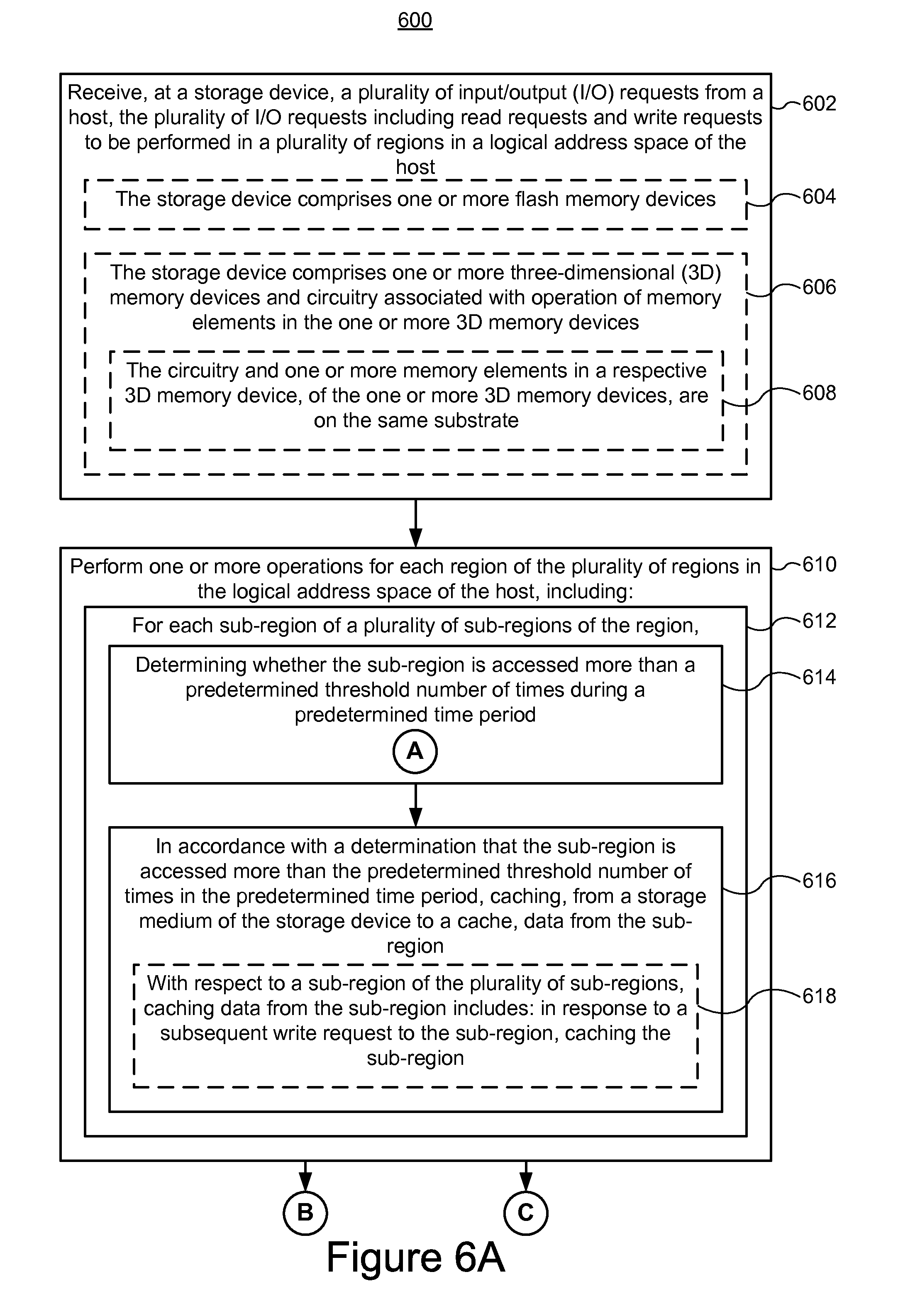
More specifically, some embodiments include a method. In some embodiments, the method includes (1) receiving, at a storage device, a plurality of input/output (I/O) requests from a host, the plurality of I/O requests including read requests and write requests to be performed in a plurality of regions in a logical address space of the host, and (2) performing one or more operations for each region of the plurality of regions in the logical address space of the host, including, for each sub-region of a plurality of sub-regions of the region: (a) determining whether the sub-region is accessed more than a predetermined threshold number of times during a predetermined time period, and (b) in accordance with a determination that the sub-region is accessed more than the predetermined threshold number of times in the predetermined time period, caching, from a storage medium of the storage device to a cache of the storage device, data from the sub-region.
In some embodiments, with respect to a sub-region of the plurality of sub-regions, caching data from the sub-region includes, in response to a subsequent write request to the sub-region, caching the sub-region.
In some embodiments, the method further includes, with respect to a sub-region of the plurality of sub-regions, subsequent to caching data from the sub-region: (1) writing subsequent write requests to the sub-region to the cache, (2) reading subsequent read requests from the sub-region from the cache, and (3) writing contents of the cache to the storage medium of the storage device in a merged operation.
In some embodiments, the method further includes, for each region of the plurality of regions in the logical address space, storing information in a data structure to maintain a history of I/O request patterns in the region for the predetermined time period.
In some embodiments, the predetermined time period is configurable.
In some embodiments, the predetermined threshold number is configurable.
In some embodiments, the storage device comprises one or more flash memory devices.
In some embodiments, the storage device comprises one or more three-dimensional (3D) memory devices and circuitry associated with operation of memory elements in the one or more 3D memory devices.
In some embodiments, the circuitry and one or more memory elements in a respective 3D memory device, of the one or more 3D memory devices, are on the same substrate.
In another aspect, any of the methods described above are performed by a storage device, the storage device including (1) one or more processors, and (2) memory storing one or more programs, which when executed by the one or more processors cause the storage device to perform or control performance of any of the methods described herein.
In yet another aspect, any of the methods described above are performed by a storage device including means for performing any of the methods described herein.
In yet another aspect, any of the methods described above are performed by a storage system comprising (1) a storage medium (e.g., comprising one or more non-volatile storage devices, such as flash memory devices) (2) one or more processors, and (3) memory storing one or more programs, which when executed by the one or more processors cause the storage system to perform or control performance of any of the methods described herein.
In yet another aspect, some embodiments include a non-transitory computer readable storage medium, storing one or more programs configured for execution by one or more processors of a storage device, the one or more programs including instructions for performing any of the methods described herein.
Numerous details are described herein in order to provide a thorough understanding of the example implementations illustrated in the accompanying drawings. However, some embodiments may be practiced without many of the specific details, and the scope of the claims is only limited by those features and aspects specifically recited in the claims. Furthermore, well-known methods, components, and circuits have not been described in exhaustive detail so as not to unnecessarily obscure more pertinent aspects of the implementations described herein.
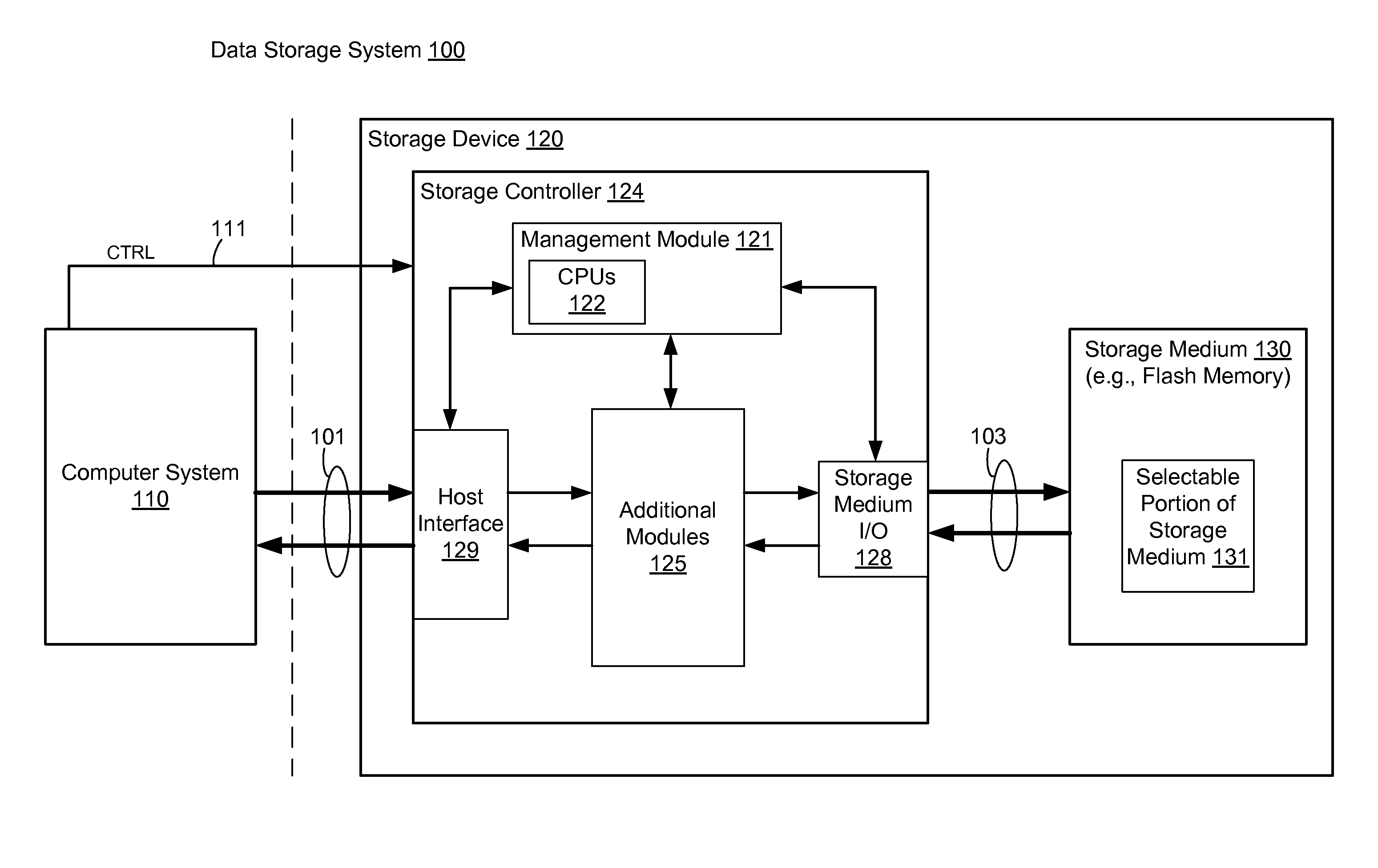
FIG. 1 is a block diagram illustrating an implementation of data storage system 100, in accordance with some embodiments. While some example features are illustrated, various other features have not been illustrated for the sake of brevity and so as not to obscure more pertinent aspects of the example implementations disclosed herein. To that end, as a non-limiting example, data storage system 100 includes a storage device 120, which includes a storage controller 124 and a storage medium 130, and is used in conjunction with a computer system 110. In some implementations, storage medium 130 is a single flash memory device while in other implementations storage medium 130 includes a plurality of flash memory devices. In some implementations, storage medium 130 is NAND-type flash memory or NOR-type flash memory. In some implementations, storage medium 130 includes one or more three-dimensional (3D) memory devices, as further defined herein. Further, in some implementations storage controller 124 is a solid-state drive (SSD) controller. However, other types of storage media may be included in accordance with aspects of a wide variety of implementations.
Computer system 110 is coupled to storage controller 124 through data connections 101. However, in some implementations computer system 110 includes storage controller 124 as a component and/or a sub-system. Computer system 110 may be any suitable computer device, such as a computer, a laptop computer, a tablet device, a netbook, an internet kiosk, a personal digital assistant, a mobile phone, a smart phone, a gaming device, a computer server, or any other computing device. Computer system 110 is sometimes called a host or host system. In some implementations, computer system 110 includes one or more processors, one or more types of memory, a display and/or other user interface components such as a keyboard, a touch screen display, a mouse, a track-pad, a digital camera and/or any number of supplemental devices to add functionality.
Storage medium 130 is coupled to storage controller 124 through connections 103. Connections 103 are sometimes called data connections, but typically convey commands in addition to data, and optionally convey metadata, error correction information and/or other information in addition to data values to be stored in storage medium 130 and data values read from storage medium 130. In some implementations, however, storage controller 124 and storage medium 130 are included in the same device as components thereof. Furthermore, in some implementations storage controller 124 and storage medium 130 are embedded in a host device, such as a mobile device, tablet, other computer or computer controlled device, and the methods described herein are performed by the embedded memory controller. Storage medium 130 may include any number (i.e., one or more) of memory devices including, without limitation, non-volatile semiconductor memory devices, such as flash memory. For example, flash memory devices can be configured for enterprise storage suitable for applications such as cloud computing, or for caching data stored (or to be stored) in secondary storage, such as hard disk drives. Additionally and/or alternatively, flash memory can also be configured for relatively smaller-scale applications such as personal flash drives or hard-disk replacements for personal, laptop and tablet computers. In some embodiments, storage medium 130 includes one or more three-dimensional (3D) memory devices, as further defined herein.
Storage medium 130 is divided into a number of addressable and individually selectable blocks, such as selectable portion 131. In some implementations, the individually selectable blocks are the minimum size erasable units in a flash memory device. In other words, each block contains the minimum number of memory cells that can be erased simultaneously. Each block is usually further divided into a plurality of pages and/or word lines, where each page or word line is typically an instance of the smallest individually accessible (readable) portion in a block. In some implementations (e.g., using some types of flash memory), the smallest individually accessible unit of a data set, however, is a sector, which is a subunit of a page. That is, a block includes a plurality of pages, each page contains a plurality of sectors, and each sector is the minimum unit of data for reading data from the flash memory device.
For example, one block comprises any number of pages, for example, 64 pages, 128 pages, 256 pages or another suitable number of pages. Blocks are typically grouped into a plurality of zones. Each block zone can be independently managed to some extent, which increases the degree of parallelism for parallel operations and simplifies management of storage medium 130.
In some implementations, storage controller 124 includes a management module 121, a host interface 129, a storage medium interface (I/O) 128, and additional module(s) 125. Storage controller 124 may include various additional features that have not been illustrated for the sake of brevity and so as not to obscure more pertinent features of the example implementations disclosed herein, and a different arrangement of features may be possible. Host interface 129 provides an interface to computer system 110 through data connections 101. Similarly, storage medium I/O 128 provides an interface to storage medium 130 though connections 103. In some implementations, storage medium I/O 128 includes read and write circuitry, including circuitry capable of providing reading signals to storage medium 130 (e.g., reading threshold voltages for NAND-type flash memory).
In some implementations, management module 121 includes one or more processing units (CPUs, also sometimes called processors) 122 configured to execute instructions in one or more programs (e.g., in management module 121). In some implementations, the one or more CPUs 122 are shared by one or more components within, and in some cases, beyond the function of storage controller 124. Management module 121 is coupled to host interface 129, additional module(s) 125 and storage medium I/O 128 in order to coordinate the operation of these components.
Additional module(s) 125 are coupled to storage medium I/O 128, host interface 129, and management module 121. As an example, additional module(s) 125 may include an error control module to limit the number of uncorrectable errors inadvertently introduced into data during writes to memory or reads from memory. In some embodiments, additional module(s) 125 are executed in software by the one or more CPUs 122 of management module 121, and, in other embodiments, additional module(s) 125 are implemented in whole or in part using special purpose circuitry (e.g., to perform encoding and decoding functions).
During a write operation, host interface 129 receives data to be stored in storage medium 130 from computer system 110. The data held in host interface 129 is made available to an encoder (e.g., in additional module(s) 125), which encodes the data to produce one or more codewords. The one or more codewords are made available to storage medium I/O 128, which transfers the one or more codewords to storage medium 130 in a manner dependent on the type of storage medium being utilized.
A read operation is initiated when computer system (host) 110 sends one or more host read commands on control line 111 to storage controller 124 requesting data from storage medium 130. Storage controller 124 sends one or more read access commands to storage medium 130, via storage medium I/O 128, to obtain raw read data in accordance with memory locations (addresses) specified by the one or more host read commands. Storage medium I/O 128 provides the raw read data (e.g., comprising one or more codewords) to a decoder (e.g., in additional module(s) 125). If the decoding is successful, the decoded data is provided to host interface 129, where the decoded data is made available to computer system 110. In some implementations, if the decoding is not successful, storage controller 124 may resort to a number of remedial actions or provide an indication of an irresolvable error condition.
Flash memory devices utilize memory cells to store data as electrical values, such as electrical charges or voltages. Each flash memory cell typically includes a single transistor with a floating gate that is used to store a charge, which modifies the threshold voltage of the transistor (i.e., the voltage needed to turn the transistor on). The magnitude of the charge, and the corresponding threshold voltage the charge creates, is used to represent one or more data values. In some implementations, during a read operation, a reading threshold voltage is applied to the control gate of the transistor and the resulting sensed current or voltage is mapped to a data value.
The terms "cell voltage" and "memory cell voltage," in the context of flash memory cells, means the threshold voltage of the memory cell, which is the minimum voltage that needs to be applied to the gate of the memory cell's transistor in order for the transistor to conduct current. Similarly, reading threshold voltages (sometimes also called reading signals, reading voltages, and/or read thresholds) applied to a flash memory cells are gate voltages applied to the gates of the flash memory cells to determine whether the memory cells conduct current at that gate voltage. In some implementations, when a flash memory cell's transistor conducts current at a given reading threshold voltage, indicating that the cell voltage is less than the reading threshold voltage, the raw data value for that read operation is a "1," and otherwise the raw data value is a "0."
As explained above, a storage medium (e.g., storage medium 130) is divided into a number of addressable and individually selectable blocks and each block is optionally (but typically) further divided into a plurality of pages and/or word lines and/or sectors. While erasure of a storage medium is performed on a block basis, in many embodiments, reading and programming of the storage medium is performed on a smaller subunit of a block (e.g., on a page basis, word line basis, or sector basis). In some embodiments, the smaller subunit of a block consists of multiple memory cells (e.g., single-level cells or multi-level cells). In some embodiments, programming is performed on an entire page. In some embodiments, a multi-level cell (MLC) NAND flash typically has four possible states per cell, yielding two bits of information per cell. Further, in some embodiments, a MLC NAND has two page types: (1) a lower page (sometimes called fast page), and (2) an upper page (sometimes called slow page).
As an example, if data is written to a storage medium in pages, but the storage medium is erased in blocks, pages in the storage medium may contain invalid (e.g., stale) data, but those pages cannot be overwritten until the whole block containing those pages is erased. In order to write to the pages with invalid data, the pages with valid data in that block are read and re-written to a new block and the old block is erased (or put on a queue for erasing). This process is called garbage collection. After garbage collection, the new block contains pages with valid data and free pages that are available for new data to be written, and the old block that was erased is also available for new data to be written. Since flash memory can only be programmed and erased a limited number of times, the efficiency of the algorithm used to pick the next block(s) to re-write and erase has a significant impact on the lifetime and reliability of flash-based storage systems.
Write amplification is a phenomenon where the actual amount of physical data written to a storage medium (e.g., storage medium 130) is a multiple of the logical amount of data intended to be written by a host (e.g., computer system 110, sometimes called a host). As discussed above, when a storage medium must be erased before it can be re-written, the garbage collection process to perform these operations results in re-writing data one or more times. This multiplying effect increases the number of writes required over the life of a storage medium, which shortens the time it can reliably operate. The formula to calculate the write amplification of a storage system is given by equation (1):
.times..times..times..times..times..times..times..times..times..times..ti- mes..times..times..times..times..times..times..times..times..times..times.- .times..times..times..times..times. ##EQU00001##
One of the goals of any storage system architecture is to reduce write amplification as much as possible so that available endurance is used to meet storage medium reliability and warranty specifications. Higher system endurance also results in lower cost as the storage system may need less over-provisioning. By reducing the write amplification, the endurance of the storage medium is increased and the overall cost of the storage system is decreased. Generally, garbage collection is performed on erase blocks with the fewest number of valid pages for best performance and best write amplification.
FIG. 2A is a block diagram illustrating an exemplary management module 121, in accordance with some embodiments. Management module 121 typically includes one or more processing units (CPUs) 122 for executing modules, programs and/or instructions stored in memory 206 and thereby performing processing operations, memory 206, and one or more communication buses 208 for interconnecting these components. Communication buses 208 optionally include circuitry (sometimes called a chipset) that interconnects and controls communications between system components. Management module 121 is coupled to host interface 129, additional module(s) 125, and storage medium I/O 128 by communication buses 208. Memory 206 includes high-speed random access memory, such as DRAM, SRAM, DDR RAM or other random access solid state memory devices, and may include non-volatile memory, such as one or more magnetic disk storage devices, optical disk storage devices, flash memory devices, or other non-volatile solid state storage devices. Memory 206 optionally includes one or more storage devices remotely located from the CPU(s) 122. Memory 206, or alternately the non-volatile memory device(s) within memory 206, comprises a non-transitory computer readable storage medium. In some embodiments, memory 206, or the computer readable storage medium of memory 206 stores the following programs, modules, and data structures, or a subset thereof: I/O receiving module 210 that is used for receiving from a host a plurality of input/output (I/O) requests (e.g., read requests and/or write requests to be performed in a plurality of regions in a logical address space of the host); translation table 212 that is used for mapping logical addresses to physical addresses (e.g., in some embodiments, translation table 212 includes forward mapping table 402, FIG. 4); data read module 214 that is used for reading data from one or more blocks in a storage medium; data write module 216 that is used for writing data to one or more blocks in a storage medium; data erase module 218 that is used for erasing data from one or more blocks in a storage medium; garbage collection module 220 that is used for garbage collection for one or more blocks in a storage medium; history maintaining module 222 that is used for maintaining a history of I/O request patterns (e.g., one or more histories of I/O request patterns) in one or more regions of a plurality of regions in a logical address space of a host; history table 224 that includes a collection of data structures (e.g., region data structures 244, FIG. 2B), each data structure storing data for a respective region of a plurality of regions in a logical address space of a host; adjustment module 226 that is used for using the history of I/O request patterns in a respective region to adjust subsequent I/O processing in the respective region; cache module 228 that is used for caching data from one or more regions (or one or more sub-regions within the one or more regions) of a plurality of regions in a logical address space of a host (e.g., from a storage medium of a storage device to a cache of the storage device); and region module 230 that is used for performing one or more operations for each region of the plurality of regions in the logical address space of the host, optionally including: determining module 232 that is used for determining, for each sub-region of a plurality of sub-regions of a respective region, whether the sub-region is accessed more than a predetermined threshold number of times during a predetermined time period; and sub-region module 234 that is used for performing one or more operations for each sub-region of a plurality of sub-regions of a respective region.
Each of the above identified elements may be stored in one or more of the previously mentioned memory devices, and corresponds to a set of instructions for performing a function described above. The above identified modules or programs (i.e., sets of instructions) need not be implemented as separate software programs, procedures or modules, and thus various subsets of these modules may be combined or otherwise re-arranged in various embodiments. In some embodiments, memory 206 may store a subset of the modules and data structures identified above. Furthermore, memory 206 may store additional modules and data structures not described above. In some embodiments, the programs, modules, and data structures stored in memory 206, or the computer readable storage medium of memory 206, provide instructions for implementing any of the methods described below with reference to FIGS. 6A-6C.
Although FIG. 2A shows management module 121 in accordance with some embodiments, FIG. 2A is intended more as a functional description of the various features which may be present in management module 121 than as a structural schematic of the embodiments described herein. In practice, and as recognized by those of ordinary skill in the art, items shown separately could be combined and some items could be separated.
FIG. 2B is a block diagram illustrating an implementation of a history table 224 included in FIG. 2A, in accordance with some embodiments. History table 224 includes a collection of region data structures 244, that each store data associated with a respective region of a plurality of regions in a logical address space of a host (e.g., a respective region 310-i of a plurality of regions in a logical address space, FIG. 3). An example of a logical address space of a host is described in further detail below with respect to FIG. 3. In some embodiments, the data stored in region data structures 244 includes information regarding real-time history of I/O request patterns per region, for each region of a plurality of regions in a logical address space. For example, without limitation, in some embodiments in which a logical address space of a host (e.g., computer system 110, FIG. 1) includes a plurality of regions (e.g., region 310-1 through region 310-m, FIG. 3), history table 224 includes at least one region data structure for each region (e.g., region data structure 244-1 for region 310-1, region data structure 244-2 for region 310-2, etc.). In some embodiments, a history of I/O request patterns is maintained for only the regions that have some I/O activity during a predetermined time period. In some embodiments, a history of I/O request patterns is maintained for a subset of all the regions in a logical address space of a host. In some embodiments, a history of I/O request patterns is maintained for all of the regions in a logical address space of a host. In some embodiments, history table 224 is maintained in one or more data structures stored on a storage device (e.g., storage device 120, FIG. 1). In some embodiments, the storage device gathers data as I/O requests are processed and stores the history of I/O request patterns and/or determinations based on the history of I/O request patterns in history table 224. In some embodiments, history table 224 is maintained in one or more data structures stored on a host (e.g., computer system 110, FIG. 1). In some embodiments, the host gathers data as I/O requests are processed and stores the history of I/O request patterns and/or determinations based on the history of I/O request patterns in history table 224. In some embodiments, one or more operations performed to gather data and/or make determinations based on the data are performed at a host (e.g., computer system 110, FIG. 1), and relevant information is transmitted to a storage device (e.g., storage device 120, FIG. 1).
In some embodiments, each region data structure (e.g., region data structure 244-i) includes information regarding real-time history of I/O request patterns for a respective region, sometimes herein called a logical address region. For example, in some embodiments, region data structure 244-1 includes information regarding real-time history of I/O request patterns for region 1 of a plurality of regions, region data structure 244-2 includes information regarding real-time history of I/O request patterns for Region 2 of the plurality of regions, and so on. In some embodiments, the history of I/O request patterns is maintained for each region for a predetermined time period (e.g., one hour). In some embodiments, the predetermined time period is configurable. In some embodiments, after the predetermined time period, the history of I/O request patterns is reset (e.g., cleared). In some embodiments, one or more parameters of region data structure 244-i are not reset until a later time. In some embodiments, some parameters of a data structure (e.g., region data structure 244-i) are reset (e.g., cleared) after the predetermined time period, while other parameters of the data structure are not reset until a later time. For example, in some embodiments, parameters tracking various count values (e.g., sequential read count 250, sequential write count 252, small write count 254, unaligned write count 256 and/or large write count 258) are reset after the predetermined time period, but if the respective region still meets certain criteria (e.g., if the respective region is still a hot region), other parameters of the data structure are not reset until a later time (e.g., hot region flag 264, FIG. 2B, is not reset until the region is no longer hot).
Region data structure 244-i illustrates an implementation of a region data structure for a respective region (e.g., region i), in accordance with some embodiments. In some embodiments, region data structure 244-i stores the following data (sometimes called history of I/O requests for a particular time period, for a particular region of the logical address space), or a subset or superset thereof: lowest LBA accessed 246 that is used for tracking a lowest logical block address (LBA) accessed in the region; highest LBA accessed 248 that is used for tracking a highest logical block address (LBA) accessed in the region; sequential read count 250 that is used for tracking a total number of sequential read requests from the region; sequential write count 252 that is used for tracking a total number of sequential write requests to the region; small write count 254 that is used for tracking a total number of write requests to write data of size less than a predefined small-size threshold; unaligned write count 256 that is used for tracking a total number of unaligned write requests to the region, wherein unaligned write requests are write requests not aligned with predefined page boundaries; large write count 258 that is used for tracking a total number of write requests to write data of size greater than a predefined large-size threshold; flags 260 that are used for tracking one or more determinations based on the history of I/O request patterns, including in some embodiments, one or more of: sequential region flag 262 that is used for tracking whether a total number of sequential I/O requests to the region has exceeded a sequential request threshold; hot region flag 264 that is used for tracking whether a total number of write requests to the region has exceeded a write threshold; valid region flag 266 that is used for tracking whether the region is accessed at least once by a plurality of I/O requests; optionally, one or more additional flags, each for tracking a corresponding determination based on the history of I/O request patterns; time stamp 268 that is used for recording a time stamp corresponding to when the history of I/O request patterns is reset; and sub-region counters 270 that are used for tracking a total number of times each sub-region (of a plurality of sub-regions in the region) is accessed.
FIG. 3 is a block diagram of a plurality of regions in a logical address space of a host, in accordance with some embodiments. In some embodiments, a logical address is the address at which an item (e.g., data stored on a memory cell) resides from the perspective of a host (e.g., computer system 110, FIG. 1). In some embodiments, a logical address differs from a physical address due to the operation of a mapping function or address translator (e.g., translation table 212, FIG. 2A, including forward mapping table 402, FIG. 4). In some embodiments, a logical block address (LBA) is mapped to a physical flash address (e.g., a physical page number (PPN), including a bank, block, and page), as described further with respect to FIG. 4.
In some embodiments, a logical address space includes a plurality of regions (e.g., region 310-1 through region 310-m), and each region includes a plurality of sub-regions (e.g., sub-region 312-1 through sub-region 312-n). In some embodiments, for example, if a storage device with an advertised capacity of 1 terabyte (TB) is divided into m regions, each region will be (1 TB)/m in size (e.g., if m=1024, each region will be (1 TB)/1024=1 gigabyte (GB) in size), and if each region is divided into n sub-regions, each sub-region will be ((1 TB)/m)/n in size (e.g., if m=1024 and n=1024, each sub-region will be ((1 TB)/1024)/1024=1 megabyte (MB) in size).
As described above with respect to FIG. 2B, in some embodiments, real-time history of I/O request patterns for a respective region is maintained for a plurality of regions in the logical address space. In some embodiments, the real-time history of I/O request patterns for a respective region (e.g., region i) is maintained in a region data structure (e.g., region data structure 244-i, FIG. 2B), which stores data corresponding to the history of I/O request patterns for the region and/or data corresponding to determinations made in accordance with the history of I/O request patterns for the region. For example, in some embodiments, real-time history of I/O request patterns for region 310-1 is maintained (e.g., in region data structure 244-1, FIG. 2B), and if a total number of write requests to region 310-1 has exceeded a write threshold during a predetermined time period, region 310-1 is marked with a hot region indicator (e.g., using hot region flag 264, FIG. 2B).
FIG. 4 is a block diagram of a forward mapping table 402, physical address space 410, and bank data 430, in accordance with some embodiments. In some embodiments, forward mapping table 402 is used to translate a logical block address (LBA) from the perspective of a host (e.g., computer system 110, FIG. 1) to a physical address in a physical address space (e.g., physical address space 410) of a storage device (e.g., storage device 120, FIG. 1). In some embodiments, an LBA is the smallest unit that is accessible by a host (e.g., 512 B). In some embodiments, LBAs are organized in numerical order in the logical address space. Using the example from FIG. 3, in some embodiments, where the logical address space includes a plurality of regions and each region is 1 GB in size, the LBAs in the first 1 GB of the logical address space are in a first region (e.g., region 310-1, FIG. 3), the LBAs in the second 1 GB of the logical address space are in a second region (e.g., region 310-2, FIG. 3), and so on.
In some embodiments, forward mapping table 402 is stored in memory associated with the storage device (e.g., in memory 206, as part of translation table 212, FIG. 2A). In some embodiments, a physical address is a physical page number (PPN), including a bank number, a block number, and a page number. In the example shown in FIG. 4, LBA 0 is mapped to bank 1 (e.g., Bank 420-1), block 3 (e.g., Block 421-3), page 37 (pages not shown in FIG. 4) of physical address space 410.
In some embodiments, bank data 430 includes information for each bank of physical address space 410 (e.g., bank 420-1 through 420-q). For example, in some embodiments, for bank i (e.g., bank 420-i), bank data 430 includes a queue of available blocks in bank i (e.g., for which to write data), a pointer to an active block in bank i (e.g., a block to which data from write requests is written), and a pointer to an active hot block in bank i (e.g., a block to which data from write requests to hot regions is written). For example, if a region (e.g., region 310-1, FIG. 3) is marked with a hot region indicator (e.g., using hot region flag 264, FIG. 2B), in some embodiments, subsequent write requests to that region are written to an active hot block. Conversely, if a region (e.g., region 310-1, FIG. 3) is not marked with a hot region indicator, in some embodiments, subsequent write requests to that region are written to an active block (sometimes referred to as an active "cold block," as opposed to an active hot block). Depending on how LBAs are mapped to banks in forward mapping table 402, each bank in physical address space 410 may need to store data specified by a write request to a region marked with a hot region indicator (sometimes referred to as a "hot region") and/or store data specified by a write request to a region not marked with a hot region indicator (sometimes referred to as a "cold region"). In some embodiments, if an LBA for a write request is from a hot region, the data specified by the write request is stored on the active hot block, and if the LBA for a write request is from a cold region, the data specified by the write request is stored on the active block (e.g., a cold block that is active). In this manner, data associated with hot regions are grouped together (e.g., on hot blocks) and data associated with cold regions are grouped together (e.g., on cold blocks).
Typically, data in hot regions are invalidated faster than data in cold regions, due to a higher frequency of updates to data in the hot regions than updates to data in the cold regions. For example, if certain popular files are accessed and edited frequently (e.g., if a user frequently accesses and edits certain documents), in some embodiments, the region of the logical address space in which those popular files reside are marked with a hot region indicator, if the region is accessed more than a predetermined threshold during a predefined period of time. In some embodiments, the LBAs of the hot region are mapped to blocks (and pages) in the physical address space (e.g., physical address space 410) of the storage device (e.g., storage device 120, FIG. 1) using a translation table (e.g., forward mapping table 402), and the open blocks associated with the hot region are marked with a hot block indicator. In some embodiments, for each bank of physical address space 410, bank data 430 includes a queue of hot blocks available for writing, with a pointer to the active hot block for storing data from write requests to a hot region. In some embodiments, for each bank of physical address space 410, bank data 430 includes a queue of cold blocks available for writing, with a pointer to the active cold block for storing data from write requests to a cold region. Since hot regions, by definition, are written to more frequently than cold regions, pages in the hot blocks are typically invalidated faster (i.e., more frequently, on average) than pages in the cold blocks. By grouping together data associated with hot regions in the hot blocks, hot blocks will typically have more invalid pages due to the frequent updating of data in the hot regions, resulting in fewer valid pages that need to be copied in a garbage collection operation. By grouping together data from cold regions in the cold blocks, cold blocks will typically have more valid pages, due to the lower frequency of updates in the cold regions than the hot regions, and will be less likely to be selected for garbage collection, reducing the movement of cold data to new blocks. This localization of writes from hot regions to hot blocks and localization of writes from cold regions to cold blocks reduces the number of blocks that require garbage collection and reduces the number of valid pages that need to be copied during garbage collection, thus reducing write amplification and improving endurance of the storage device.
Although the description herein uses examples in which regions are separated into two categories (e.g., hot or cold) and blocks are separated into two categories accordingly, those skilled in the art will appreciate that the embodiments described herein may be extended to more than two categories (e.g., three categories for regions and associated blocks, including hot, warm, and cold).
FIG. 5 is a block diagram of a cache 500 with a cached sub-region 510, in accordance with some embodiments. In some embodiments, cache 500 is included in a storage device (e.g., storage device 120, FIG. 1). In some embodiments, cache 500 is implemented in one or more volatile random access memory devices, such as, without limitation, DRAM or SRAM devices. In some embodiments, cache 500 is physically external to a storage device (e.g., external to storage device 120, FIG. 1). For example, in some embodiments, cache 500 is located in a DRAM device external to the storage device, where the DRAM device may be sized differently for different customers. In some other embodiments, cache 500 is physically part of the storage device.
In some embodiments, sub-regions that meet predefined criteria (e.g., sub-regions that are accessed more than a predetermined threshold number of times and/or sub-regions that have a history of unaligned write requests) are cached to cache 500. For example, in some embodiments, if a region (e.g., region 310-2, FIG. 3) has a history of unaligned write requests (e.g., determined from unaligned write count 256, FIG. 2B), where unaligned write requests are write requests not aligned with predefined page boundaries, a sub-region in that region (e.g., sub-region 312-3, FIG. 3) that is accessed more than a predetermined threshold number of times is cached to cache 500. In some embodiments, the predefined page boundaries are defined with respect to the logical address space of the host. In one example, in which L logical blocks (e.g., 8 blocks) are mapped to each physical page in storage medium 130, the predefined page boundaries are the logical addresses of the first (or last) location in each set of L logical blocks. Restated, in this example, the predefined page boundaries are logical addresses in the logical address space that are positive integer multiples of L*B, where B is the size of one logical block and L is the number of logical blocks mapped to each physical page in storage medium 130. In a more specific example, the predefined page boundaries are logical addresses that are positive integer multiples of 4 KB (i.e., 4098 bytes).
I/O alignment refers to whether the starting address of an I/O request is a multiple of the smallest unit size of a storage medium (e.g., aligned with a 4 KB page of a NAND flash memory device). For every misaligned write, the storage device must perform at least one read-modify-write operation on data stored in non-volatile memory. For example, an unaligned write request spanning pages 0 through 2 (depicted by the dotted box in cached sub-region 510) normally requires two read-modify-write operations on data stored in non-volatile memory, since the unaligned write request is only modifying a portion of page 0 and a portion of page 2. In some embodiments, since a program (e.g., write) operation is performed on an entire (erased) page, the storage device first reads page 0 to determine the portion of data that is not modified, modifies the portion of data that is affected by the unaligned write request, writes the data to a new page location, and invalidates page 0. A similar process is needed for page 2. However, in some embodiments, if sub-region 510 is cached, unaligned writes are processed in the cache, and may then be written to a storage medium (e.g., storage medium 130, FIG. 1) in a merged operation, thus reducing or avoiding read-modify-write operations on data stored in non-volatile memory.
FIGS. 6A-6C illustrate a flowchart representation of a memory management method 600, in accordance with some embodiments. At least in some embodiments, method 600 is performed by a storage device (e.g., storage device 120, FIG. 1) or one or more components of the storage device (e.g., storage controller 124 and/or storage medium 130, FIG. 1), wherein the storage device is operatively coupled with a host system (e.g., computer system 110, FIG. 1). In some embodiments, method 600 is governed by instructions that are stored in a non-transitory computer readable storage medium and that are executed by one or more processors of a device, such as the one or more processing units (CPUs) 122 of management module 121, shown in FIGS. 1 and 2A. In some embodiments, method 600 is performed by a storage system (e.g., data storage system 100, FIG. 1) or one or more components of the storage system (e.g., computer system 110 and/or storage device 120, FIG. 1). In some embodiments, some of the operations of method 600 are performed at a host (e.g., computer system 110, FIG. 1) and information is transmitted to a storage device (e.g., storage device 120, FIG. 1). In some embodiments, method 600 is governed, at least in part, by instructions that are stored in a non-transitory computer readable storage medium and that are executed by one or more processors of a host (not shown in FIG. 1). For ease of explanation, the following describes method 600 as performed by a storage device (e.g., storage device 120, FIG. 1). However, those skilled in the art will appreciate that in other embodiments, one or more of the operations described in method 600 are performed by a host (e.g., computer system 110, FIG. 1).
A storage device (e.g., storage device 120, FIG. 1) receives (602) a plurality of input/output (I/O) requests from a host (e.g., computer system 110, FIG. 1), the plurality of I/O requests including read requests and write requests to be performed in a plurality of regions in a logical address space of the host. In some embodiments, the I/O requests specify operations (sometimes called storage operations or memory operations) to be performed with respect to logical addresses in a plurality of regions in a logical address space of a host (e.g., regions 310, FIG. 3). In some embodiments, the plurality of I/O requests includes read requests from one or more regions of the plurality of regions and write requests to one or more regions of the plurality of regions. For example, in some embodiments, the plurality of I/O requests includes one or more read requests from one or more regions of the plurality of regions (e.g., regions 310, FIG. 3) and one or more write requests to one or more regions of the plurality of regions. In some embodiments, an I/O receiving module (e.g., I/O receiving module 210, FIG. 2A) is used to receive a plurality of input/output (I/O) requests from a host, the plurality of I/O requests including read requests and write requests to be performed in a plurality of regions in a logical address space of the host, as described above with respect to FIG. 2A.
In some embodiments, the storage device comprises (604) one or more flash memory devices. In some embodiments, the storage device comprises a storage medium (e.g., storage medium 130, FIG. 1), and the storage medium comprises one or more non-volatile storage devices, such as flash memory devices. In some embodiments, the storage medium (e.g., storage medium 130, FIG. 1) is a single flash memory device, while in other embodiments the storage medium includes a plurality of flash memory devices. For example, in some implementations, the storage medium includes dozens or hundreds of flash memory devices, organized in parallel memory channels, such as 16, 32 or 64 flash memory devices per memory channel, and 8, 16 or 32 parallel memory channels. In some embodiments, the non-volatile storage medium (e.g., storage medium 130, FIG. 1) includes NAND-type flash memory or NOR-type flash memory. In other embodiments, the storage medium comprises one or more other types of non-volatile storage devices.
In some embodiments, the storage device comprises (606) one or more three-dimensional (3D) memory devices, as further defined herein, and circuitry associated with operation of memory elements in the one or more 3D memory devices. In some embodiments, the storage device comprises a storage medium (e.g., storage medium 130, FIG. 1), and the storage medium comprises one or more 3D memory devices and circuitry associated with operation of memory elements in the one or more 3D memory devices. In some embodiments, the storage medium (e.g., storage medium 130, FIG. 1) is a single 3D memory device, while in other embodiments the storage medium includes a plurality of 3D memory devices.
In some embodiments, the circuitry and one or more memory elements in a respective 3D memory device, of the one or more 3D memory devices, are (608) on the same substrate (e.g., a silicon substrate). In some embodiments, the substrate is a wafer on which the material layers of the one or more memory elements are deposited and/or in which the one or more memory elements are formed. In some embodiments, the substrate is a carrier substrate which is attached to the one or more memory elements after they are formed. As a non-limiting example, in some embodiments, the substrate includes a semiconductor such as silicon.
The storage device performs (610) one or more operations for each region of the plurality of regions in the logical address space of the host, including, for each sub-region of a plurality of sub-regions of the region (612): (1) determining (614) whether the sub-region is accessed more than a predetermined threshold number of times during a predetermined time period, and (2) in accordance with a determination that the sub-region is accessed more than the predetermined threshold number of times in the predetermined time period, caching (616), from a storage medium of the storage device to a cache of the storage device, data from the sub-region. In some embodiments, the plurality of regions includes only regions that have some I/O activity during a predetermined time period. For example, in some embodiments, the one or more operations are performed only for regions that have I/O activity during a predetermined time period. Thus, in some embodiments, the plurality of regions is a subset of all the regions in the logical address space. For example, in some embodiments, the one or more operations are performed for a subset of all the regions in the logical address space (e.g., when only a subset of all the regions in the logical address space has I/O activity during the predetermined time period). In some embodiments, the plurality of regions is all of the regions in the logical address space. For example, in some embodiments, the one or more operations are performed for all of the regions in the logical address space. In some embodiments, a region module (e.g., region module 230, FIG. 2A), including an optional determining module (e.g., determining module 232, FIG. 2A) and/or an optional sub-region module (e.g., sub-region module 234, FIG. 2A), and/or a cache module (e.g., cache module 228, FIG. 2A) are used to perform one or more operations for each region of the plurality of regions in the logical address space of the host, including, for each sub-region of a plurality of sub-regions of the region: (1) determining whether the sub-region is accessed more than a predetermined threshold number of times during a predetermined time period, and (2) in accordance with a determination that the sub-region is accessed more than the predetermined threshold number of times in the predetermined time period, caching, from a storage medium of the storage device to a cache of the storage device, data from the sub-region, as described above with respect to FIG. 2A.
In some embodiments, some (e.g., one, some, or all) of the operations performed for each region of the plurality of regions in the logical address space of the host are performed at the storage device (e.g., storage device 120, FIG. 1). In some embodiments, some (e.g., one, some, or all) of the operations performed for each region of the plurality of regions in the logical address space of the host are performed at the host (e.g., computer system 110, FIG. 1). In some embodiments, one or more of the operations are performed at the storage device (e.g., storage device 120, FIG. 1) and one or more of the operations are performed at the host (e.g., computer system 110, FIG. 1). For ease of explanation, the description herein describes embodiments wherein the one or more operations are performed at the storage device. However, in some embodiments, one or more of the operations are performed at the host and signals and/or commands are transmitted to the storage device as needed. For example, in some embodiments, maintaining a history of I/O request patterns in the region for a predetermined time period and/or making determinations based on the history of I/O request patterns (e.g., determining whether a sub-region is accessed more than a predetermined threshold number of times during a predetermined time period) is performed at the host and one or more signals (e.g., a command, a flag, etc.) is transmitted by the host to the storage device to either adjust subsequent I/O processing in the region or to communicate to the storage device one or more aspects of the history of I/O request patterns in the region (e.g., including one or more aspects of the history of I/O request patterns in one or more sub-regions of the region).
As noted above, for each sub-region of a plurality of sub-regions of the region (612), the storage device determines (614) whether the sub-region is accessed more than a predetermined threshold number of times during a predetermined time period. In some embodiments, determining whether the sub-region is accessed more than a predetermined threshold number of times during a predetermined time period includes determining whether the sub-region is accessed by the plurality of I/O requests more than a predetermined threshold number of times during a predetermined time period. In some embodiments, the plurality of I/O requests includes read requests from the sub-region and/or write requests to the sub-region. In some embodiments, determining whether the sub-region is accessed more than a predetermined threshold number of times during a predetermined time period is based on information (e.g., data gathered regarding I/O requests for the sub-region) stored in a data structure (e.g., region data structure 244-i, FIG. 2B) for maintaining a history of I/O request patterns in a respective region for the predetermined time period. In some embodiments, a determining module (determining module 232, FIG. 2A) is used to determine, for each sub-region of a plurality of sub-regions of the region, whether the sub-region is accessed more than a predetermined threshold number of times during a predetermined time period, as described above with respect to FIG. 2A.
In some embodiments, with respect to a sub-region of the plurality of sub-regions, determining whether the sub-region is accessed more than the predetermined threshold number of times includes tracking whether a total number of read requests to the sub-region has exceeded a read threshold during the aforementioned time period. In some embodiments, with respect to a sub-region of the plurality of sub-regions, determining whether the sub-region is accessed more than the predetermined threshold number of times includes tracking whether a total number of write requests to the sub-region has exceeded a write threshold during the aforementioned time period. In some embodiments, with respect to a sub-region of the plurality of sub-regions, determining whether the sub-region is accessed more than the predetermined threshold number of times includes tracking whether a total number of requests (e.g., both read and write requests) to the sub-region has exceeded a request threshold during the aforementioned time period. In some embodiments, tracking whether a total number of requests (e.g., read requests, write requests, or read and write requests combined) to the sub-region has exceeded a predetermined threshold includes recording updated values for the total number of requests (e.g., read requests, write requests, or read and write requests combined) to the sub-region. For example, in some embodiments, tracking whether a total number of requests to sub-region 312-1 (FIG. 3) has exceeded a predetermined threshold includes recording updated values for the total number of requests to sub-region 312-1 (e.g., using one of sub-region counters 270 in region data structure 244-i, FIG. 2B). In some embodiments, the total number of requests to the sub-region is tracked and/or recorded using a parameter stored in a data structure (e.g., region data structure 244-i, FIG. 2B). In some embodiments, a determination of whether a total number of requests to the sub-region has exceeded a predetermined threshold is tracked and/or recorded using a parameter stored in a data structure (e.g., using one of flags 260 in region data structure 244-i, FIG. 2B).
In some embodiments, the predetermined time period is (620) configurable. For example, in some embodiments, the predetermined time period is configurable during initialization of the storage device (e.g., storage device 120, FIG. 1). As another example, in some embodiments, the predetermined time period is configurable during each power cycle of the storage device. In some embodiments, the predetermined time period is configurable using a configuration parameter, for example a configuration parameter specified by a command sent by a host system (e.g., computer system 110, FIG. 1). In some embodiments, the predetermined time period is configured to be a fixed number. In some embodiments, the predetermined time period is configured based on how long the history of I/O request patterns is to be maintained before resetting (e.g., clearing) the history (e.g., in region data structure 244-i, FIG. 2B). In some embodiments, some parameters of a data structure (e.g., region data structure 244-i, FIG. 2B) are reset (e.g., cleared) after the predetermined time period, while other parameters of the data structure are not reset until a later time. For example, in some embodiments, flags 260 are re-evaluated and set accordingly at the end of each predetermined time period based on the count values at the end of the predetermined time period, and parameters tracking various count values (e.g., sequential read count 250, sequential write count 252, small write count 254, unaligned write count 256 and/or large write count 258, FIG. 2B) are reset after the predetermined time period. Thus, if (i.e., in accordance with a determination that) the respective region still meets certain criteria (e.g., if the respective region is still a hot region), one or more other parameters (e.g., one or more respective flags 260) of the data structure are not reset until a later time (e.g., hot region flag 264, FIG. 2B, is not reset until the region is no longer hot). As a result, the respective time period used to determine whether to adjust a particular type of I/O operation may encompass both the prior predetermined time period (e.g., a one hour time period preceding the current one hour time period) and the current predetermined time period.
In some embodiments, the predetermined threshold number is (622) configurable. For example, in some embodiments, the predetermined threshold number is configurable during initialization of the storage device (e.g., storage device 120, FIG. 1). As another example, in some embodiments, the predetermined threshold number is configurable during each power cycle of the storage device. In some embodiments, the predetermined threshold number is configurable using a configuration parameter, for example a configuration parameter specified by a command sent by a host system (e.g., computer system 110, FIG. 1). In some embodiments, the predetermined threshold number is configured to be a fixed number.
As noted above, the storage device, in accordance with a determination that the sub-region is accessed more than the predetermined threshold number of times in the predetermined time period, caches (616), from a storage medium (e.g., storage medium 130, FIG. 1) of the storage device to a cache (e.g., cache 500, FIG. 5) of the storage device, data from the sub-region. In some embodiments, the storage device caches data from the sub-region for the remainder of the predetermined time period. In some embodiments, the storage device also caches data from the sub-region for a next instance of the predetermined time period. In some embodiments, the storage device caches a predefined amount of data, such as all the pages on a word line, from the storage medium of the storage device. In some embodiments, the storage device caches an entire sub-region (e.g., the sub-region that is accessed more than the predetermined threshold number of times in the predetermined time period). For example, in some embodiments, the storage device, in accordance with a determination that sub-region 312-3 (FIG. 3) is accessed more than the predetermined threshold number of times during the predetermined time period, caches, from a storage medium (e.g., storage medium 130, FIG. 1) of the storage device to a cache (e.g., cache 500, FIG. 5) of the storage device, data from sub-region 312-3 (e.g., stored as cached sub-region 510, FIG. 5). In a further example, the cached data is retained in the cache until occurrence of a trigger condition, such as the cached data being evicted from the cache due to normal cache maintenance operations. In another example, the trigger condition is a determination that the aforementioned conditions for caching the data no longer exist, which may be determined, for example, at the end or beginning of a respective predetermined time period. In some embodiments, a sub-region module (e.g., sub-region module 234, FIG. 2A) and/or a cache module (e.g., cache module 228, FIG. 2A) are used to, in accordance with a determination that the sub-region is accessed more than the predetermined threshold number of times in the predetermined time period, cache, from a storage medium of the storage device to a cache of the storage device, data from the sub-region, as described above with respect to FIG. 2A.
Alternatively, in some embodiments, the storage device, for each region of the plurality of regions in the logical address space of the host: (1) determines one or more sub-regions of a plurality of sub-regions within the region that are accessed more than a predetermined threshold number of times during the predetermined time period, and (2) caches, from a storage medium (e.g., storage medium 130, FIG. 1) of the storage device to a cache (e.g., cache 500, FIG. 5) of the storage device, data from the determined one or more sub-regions. In some embodiments, the storage device caches data from the determined one or more sub-regions for the remainder of the predetermined time period. In some embodiments, the storage device also caches data from the determined one or more sub-regions for a next instance of the predetermined time period. In some embodiments, the storage device caches a predefined amount of data, such as all the pages on a word line, from the storage medium of the storage device. In some embodiments, the storage device caches an entire sub-region (e.g., one of the determined one or more sub-regions). For example, in some embodiments, the storage device, (1) determines sub-region 312-3 (FIG. 3) is accessed more than a predetermined threshold number of times during the predetermined time period, and (2) caches, from a storage medium (e.g., storage medium 130, FIG. 1) of the storage device to a cache (e.g., cache 500, FIG. 5) of the storage device, data from sub-region 312-3 (e.g., stored as cached sub-region 510, FIG. 5). In a further example, the cached data is retained in the cache until occurrence of a trigger condition, such as the cached data being evicted from the cache due to normal cache maintenance operations. In another example, the trigger condition is a determination that the aforementioned conditions for caching the data no longer exist, which may be determined, for example, at the end or beginning of a respective predetermined time period. In some embodiments, a sub-region module (e.g., sub-region module 234, FIG. 2A) and/or a cache module (e.g., cache module 228, FIG. 2A) are used to, for each region of the plurality of regions in the logical address space of the host: (1) determine one or more sub-regions of a plurality of sub-regions within the region that are accessed more than a predetermined threshold number of times during the predetermined time period, and (2) cache, from a storage medium of the storage device to a cache of the storage device, data from the determined one or more sub-regions, as described above with respect to FIG. 2A.
In some embodiments, with respect to a sub-region of the plurality of sub-regions, caching data from the sub-region includes (618), in response to a subsequent write request to the sub-region, caching the sub-region (i.e., caching data from the sub-region to a cache of the storage device). For example, in some embodiments, the storage device, in response to a subsequent write request to sub-region 312-3 (FIG. 3), caches sub-region 312-3 (e.g., stored as cached sub-region 510, FIG. 5). In some embodiments, the storage device caches the sub-region for the remainder of the predetermined time period. In some embodiments, the storage device also caches the sub-region for a next instance of the predetermined time period. In one example, the cached sub-region is retained in the cache until occurrence of a trigger condition, such as the cached sub-region being evicted from the cache due to normal cache maintenance operations. In another example, the trigger condition is a determination that the aforementioned conditions for caching the sub-region no longer exist, which may be determined, for example, at the end or beginning of a respective predetermined time period.
In some embodiments, with respect to a sub-region of the plurality of sub-regions, subsequent to caching data from the sub-region (624), the storage device (1) writes subsequent write requests to the sub-region to the cache, (2) reads subsequent read requests from the sub-region from the cache, and (3) writes contents of the cache to the storage medium of the storage device in a merged operation. Using the example above where sub-region 312-3 (FIG. 3) is cached to cache 500 (FIG. 5) (e.g., stored as cached sub-region 510, FIG. 5), in some embodiments, subsequent to caching data from sub-region 312-3, the storage device (1) writes subsequent write requests to sub-region 312-3 to cache 500 (e.g., writes one or more pages to cached sub-region 510, FIG. 5), (2) reads subsequent read requests from sub-region 312-3 from cache 500 (e.g., reads one or more pages from cached sub-region 510, FIG. 5), and (3) writes contents of cache 500 (e.g., cached sub-region 510, FIG. 5) to the storage medium (e.g., storage medium 130, FIG. 1) of the storage device in a merged operation. In a further example, the writing of the contents of the cache occurs upon occurrence of a trigger condition, such as the contents of the cache being evicted from the cache due to normal cache maintenance operations. In another example, the trigger condition is a determination that the aforementioned conditions for caching data from the sub-region no longer exist, which may be determined, for example, at the end or beginning of a respective predetermined time period. In some embodiments, a sub-region module (e.g., sub-region module 234, FIG. 2A) and/or a data write module (e.g., data write module 216, FIG. 2A) are used to, with respect to a sub-region of the plurality of sub-regions, subsequent to caching data from the sub-region, (1) write subsequent write requests to the sub-region to the cache, (2) read subsequent read requests from the sub-region from the cache, and (3) write contents of the cache to the storage medium of the storage device in a merged operation, as described above with respect to FIG. 2A.
In some embodiments, for each sub-region of the plurality of sub-regions of a respective region, the storage device sets a flag to denote the determination of whether the sub-region is accessed more than a predetermined threshold number of times during the predetermined time period. In some embodiments, setting a flag to denote the determination of whether the sub-region is accessed more than a predetermined threshold number of times during the predetermined time period includes storing a flag (e.g., one of flags 260, FIG. 2B) or other marker for the sub-region. In some embodiments, setting a flag to denote the determination of whether the sub-region is accessed more than a predetermined threshold number of times during the predetermined time period includes setting the flag to "true" or "1" (as opposed to "false" or "0") in accordance with a determination that the sub-region is accessed more than a predetermined threshold number of times during the predetermined time period. For example, in some embodiments, in accordance with a determination that sub-region 312-3 (FIG. 3) is accessed more than a predetermined threshold number of times during the predetermined time period, the storage device sets a flag (e.g., one of flags 260, FIG. 2B) to "1" in the region data structure associated with the region including sub-region 312-3, which is region 310-2 (e.g., in region data structure 244-2, FIG. 2B). In some embodiments, the flag to denote the determination of whether the sub-region is accessed more than a predetermined threshold number of times during the predetermined time period is set for the remainder of the predetermined time period. In some embodiments, the flag to denote the determination of whether the sub-region is accessed more than a predetermined threshold number of times during the predetermined time period remains set for a next instance of the predetermined time period. In some embodiments, a region module (e.g., region module 230, FIG. 2A) and/or a sub-region module (e.g., sub-region module 234, FIG. 2A) are used to set, for each sub-region of the plurality of sub-regions of a respective region, a flag to denote the determination of whether the sub-region is accessed more than a predetermined threshold number of times during the predetermined time period, as described above with respect to FIG. 2A.
As discussed above, in some embodiments, flags (e.g., flags 260, FIG. 2B) are re-evaluated and set accordingly at the end of each predetermined time period based on the count values at the end of the predetermined time period. As a result, in some embodiments, flags are set based on the history of I/O requests in the current predetermined time period and/or based on the history of I/O requests in the prior predetermined time period. In one example that uses one hour time periods as the predetermined time period, the number of times a respective sub-region is accessed is determined to have exceeded a predetermined threshold number of times part-way through a one hour time period. As a result, the respective flag (e.g., one of flags 260, FIG. 2B) for that logical address region (including the respective sub-region) remains set both during the remainder of the one hour time period, and also through the next one hour time period (at which point it would be re-evaluated based on activity during that next one hour time period).
In some embodiments, the storage device, for each region of the plurality of regions in the logical address space, stores (626) information (e.g., data gathered regarding the plurality of I/O requests) in a data structure (e.g., history table 224, FIG. 2A) to maintain a history of I/O request patterns in the region for the predetermined time period. For example, in some embodiments, the storage device stores information in region data structure 244-1 (FIG. 2B) to maintain a history of I/O request patterns in region 310-1 (FIG. 3) for the predetermined time period. In some embodiments, maintaining a history of I/O request patterns in the region for the predetermined time period includes gathering the historical data as I/O requests are received and/or processed. For example, in some embodiments, maintaining a history of I/O request patterns in region 310-1 (FIG. 3) includes gathering the historical data as read requests from and write requests to region 310-1 are received and/or processed. In some embodiments, the information is stored in a data structure stored on the storage device (e.g., storage device 120, FIG. 1). For example, in some embodiments, the history of I/O request patterns is maintained in a history table (e.g., history table 224, FIGS. 2A and 2B) stored on the storage device (e.g., in memory 206 of management module 121 of storage controller 124 of storage device 120, FIG. 1). In some embodiments, the storage device gathers data as I/O requests are processed and stores the history of I/O request patterns and/or determinations based on the history of I/O request patterns in a history table (e.g., history table 224, FIGS. 2A and 2B) stored on the storage device. In some embodiments, the history table includes one or more data structures. In some embodiments, one or more operations performed to gather data and/or make determinations based on the data are performed at a host (e.g., computer system 110, FIG. 1), relevant information is transmitted from the host to a storage device (e.g., storage device 120, FIG. 1), and the history of I/O request patterns is maintained in a data structure on the storage device. In some embodiments, the information is stored in a data structure stored on the host (e.g., computer system 110, FIG. 1). For example, in some embodiments, the history of I/O request patterns is maintained in a history table stored on the host. In some embodiments, the host gathers data as I/O requests are processed and stores the history of I/O request patterns and/or determinations based on the history of I/O request patterns in a history table stored on the host. In some embodiments, the history table includes one or more data structures. In some embodiments, a history maintaining module (e.g., history maintaining module 222, FIG. 2A) is used to store, for each region of the plurality of regions in the logical address space, information in a data structure to maintain a history of I/O request patterns in the region for the predetermined time period, as described above with respect to FIG. 2A.
In some embodiments, any of the methods described above are performed by a storage device, the storage device including (1) one or more processors, and (2) memory storing one or more programs, which when executed by the one or more processors cause the storage device to perform or control performance of any of the methods described herein.
In some embodiments, any of the methods described above are performed by a storage system comprising (1) a storage medium (e.g., comprising one or more non-volatile storage devices, such as flash memory devices) (2) one or more processors, and (3) memory storing one or more programs, which when executed by the one or more processors cause the storage system to perform or control performance of any of the methods described herein.
Semiconductor memory devices include volatile memory devices, such as dynamic random access memory ("DRAM") or static random access memory ("SRAM") devices, non-volatile memory devices, such as resistive random access memory ("ReRAM"), electrically erasable programmable read only memory ("EEPROM"), flash memory (which can also be considered a subset of EEPROM), ferroelectric random access memory ("FRAM"), and magnetoresistive random access memory ("MRAM"), and other semiconductor elements capable of storing information. Each type of memory device may have different configurations. For example, flash memory devices may be configured in a NAND or a NOR configuration.
The memory devices can be formed from passive and/or active elements, in any combinations. By way of non-limiting example, passive semiconductor memory elements include ReRAM device elements, which in some embodiments include a resistivity switching storage element, such as an anti-fuse, phase change material, etc., and optionally a steering element, such as a diode, etc. Further by way of non-limiting example, active semiconductor memory elements include EEPROM and flash memory device elements, which in some embodiments include elements containing a charge storage region, such as a floating gate, conductive nanoparticles, or a charge storage dielectric material.
Multiple memory elements may be configured so that they are connected in series or so that each element is individually accessible. By way of non-limiting example, flash memory devices in a NAND configuration (NAND memory) typically contain memory elements connected in series. A NAND memory array may be configured so that the array is composed of multiple strings of memory in which a string is composed of multiple memory elements sharing a single bit line and accessed as a group. Alternatively, memory elements may be configured so that each element is individually accessible (e.g., a NOR memory array). NAND and NOR memory configurations are exemplary, and memory elements may be otherwise configured.
The semiconductor memory elements located within and/or over a substrate may be arranged in two or three dimensions, such as a two dimensional memory structure or a three dimensional memory structure.
In a two dimensional memory structure, the semiconductor memory elements are arranged in a single plane or a single memory device level. Typically, in a two dimensional memory structure, memory elements are arranged in a plane (e.g., in an x-z direction plane) which extends substantially parallel to a major surface of a substrate that supports the memory elements. The substrate may be a wafer over or in which the layer of the memory elements are formed or it may be a carrier substrate which is attached to the memory elements after they are formed. As a non-limiting example, the substrate may include a semiconductor such as silicon.
The memory elements may be arranged in the single memory device level in an ordered array, such as in a plurality of rows and/or columns. However, the memory elements may be arrayed in non-regular or non-orthogonal configurations. The memory elements may each have two or more electrodes or contact lines, such as bit lines and word lines.
A three dimensional memory array is arranged so that memory elements occupy multiple planes or multiple memory device levels, thereby forming a structure in three dimensions (i.e., in the x, y and z directions, where the y direction is substantially perpendicular and the x and z directions are substantially parallel to the major surface of the substrate).
As a non-limiting example, a three dimensional memory structure may be vertically arranged as a stack of multiple two dimensional memory device levels. As another non-limiting example, a three dimensional memory array may be arranged as multiple vertical columns (e.g., columns extending substantially perpendicular to the major surface of the substrate, i.e., in the y direction) with each column having multiple memory elements in each column. The columns may be arranged in a two dimensional configuration (e.g., in an x-z plane), resulting in a three dimensional arrangement of memory elements with elements on multiple vertically stacked memory planes. Other configurations of memory elements in three dimensions can also constitute a three dimensional memory array.
By way of non-limiting example, in a three dimensional NAND memory array, the memory elements may be coupled together to form a NAND string within a single horizontal (e.g., x-z) memory device level. Alternatively, the memory elements may be coupled together to form a vertical NAND string that traverses across multiple horizontal memory device levels. Other three dimensional configurations can be envisioned wherein some NAND strings contain memory elements in a single memory level while other strings contain memory elements which span through multiple memory levels. Three dimensional memory arrays may also be designed in a NOR configuration and in a ReRAM configuration.
Typically, in a monolithic three dimensional memory array, one or more memory device levels are formed above a single substrate. Optionally, the monolithic three dimensional memory array may also have one or more memory layers at least partially within the single substrate. As a non-limiting example, the substrate may include a semiconductor such as silicon. In a monolithic three dimensional array, the layers constituting each memory device level of the array are typically formed on the layers of the underlying memory device levels of the array. However, layers of adjacent memory device levels of a monolithic three dimensional memory array may be shared or have intervening layers between memory device levels.
Then again, two dimensional arrays may be formed separately and then packaged together to form a non-monolithic memory device having multiple layers of memory. For example, non-monolithic stacked memories can be constructed by forming memory levels on separate substrates and then stacking the memory levels atop each other. The substrates may be thinned or removed from the memory device levels before stacking, but as the memory device levels are initially formed over separate substrates, the resulting memory arrays are not monolithic three dimensional memory arrays. Further, multiple two dimensional memory arrays or three dimensional memory arrays (monolithic or non-monolithic) may be formed on separate chips and then packaged together to form a stacked-chip memory device.
Associated circuitry is typically required for operation of the memory elements and for communication with the memory elements. As non-limiting examples, memory devices may have circuitry used for controlling and driving memory elements to accomplish functions such as programming and reading. This associated circuitry may be on the same substrate as the memory elements and/or on a separate substrate. For example, a controller for memory read-write operations may be located on a separate controller chip and/or on the same substrate as the memory elements.
The term "three-dimensional memory device" (or 3D memory device) is herein defined to mean a memory device having multiple memory layers or multiple levels (e.g., sometimes called multiple memory device levels) of memory elements, including any of the following: a memory device having a monolithic or non-monolithic 3D memory array, some non-limiting examples of which are described above; or two or more 2D and/or 3D memory devices, packaged together to form a stacked-chip memory device, some non-limiting examples of which are described above.
One of skill in the art will recognize that this invention is not limited to the two dimensional and three dimensional exemplary structures described but cover all relevant memory structures within the spirit and scope of the invention as described herein and as understood by one of skill in the art.
It will be understood that, although the terms "first," "second," etc. may be used herein to describe various elements, these elements should not be limited by these terms. These terms are only used to distinguish one element from another. For example, a first region could be termed a second region, and, similarly, a second region could be termed a first region, without changing the meaning of the description, so long as all occurrences of the "first region" are renamed consistently and all occurrences of the "second region" are renamed consistently. The first region and the second region are both regions, but they are not the same region.
The terminology used herein is for the purpose of describing particular embodiments only and is not intended to be limiting of the claims. As used in the description of the embodiments and the appended claims, the singular forms "a," "an" and "the" are intended to include the plural forms as well, unless the context clearly indicates otherwise. It will also be understood that the term "and/or" as used herein refers to and encompasses any and all possible combinations of one or more of the associated listed items. It will be further understood that the terms "comprises" and/or "comprising," when used in this specification, specify the presence of stated features, integers, steps, operations, elements, and/or components, but do not preclude the presence or addition of one or more other features, integers, steps, operations, elements, components, and/or groups thereof.
As used herein, the term "if" may be construed to mean "when" or "upon" or "in response to determining" or "in accordance with a determination" or "in response to detecting," that a stated condition precedent is true, depending on the context. Similarly, the phrase "if it is determined [that a stated condition precedent is true]" or "if [a stated condition precedent is true]" or "when [a stated condition precedent is true]" may be construed to mean "upon determining" or "in response to determining" or "in accordance with a determination" or "upon detecting" or "in response to detecting" that the stated condition precedent is true, depending on the context.
The foregoing description, for purpose of explanation, has been described with reference to specific embodiments. However, the illustrative discussions above are not intended to be exhaustive or to limit the claims to the precise forms disclosed. Many modifications and variations are possible in view of the above teachings. The embodiments were chosen and described in order to best explain principles of operation and practical applications, to thereby enable others skilled in the art.
* * * * *
References
D00000
D00001
D00002
D00003
D00004
D00005
D00006
D00007
D00008
D00009
M00001
XML
uspto.report is an independent third-party trademark research tool that is not affiliated, endorsed, or sponsored by the United States Patent and Trademark Office (USPTO) or any other governmental organization. The information provided by uspto.report is based on publicly available data at the time of writing and is intended for informational purposes only.
While we strive to provide accurate and up-to-date information, we do not guarantee the accuracy, completeness, reliability, or suitability of the information displayed on this site. The use of this site is at your own risk. Any reliance you place on such information is therefore strictly at your own risk.
All official trademark data, including owner information, should be verified by visiting the official USPTO website at www.uspto.gov. This site is not intended to replace professional legal advice and should not be used as a substitute for consulting with a legal professional who is knowledgeable about trademark law.