Methods of forming and using fuses
Redaelli , et al.
U.S. patent number 10,290,456 [Application Number 15/339,699] was granted by the patent office on 2019-05-14 for methods of forming and using fuses. This patent grant is currently assigned to Micron Technology, Inc.. The grantee listed for this patent is Micron Technology, Inc.. Invention is credited to Andrea Redaelli, Giorgio Servalli.
| United States Patent | 10,290,456 |
| Redaelli , et al. | May 14, 2019 |
Methods of forming and using fuses
Abstract
Some embodiments include a fuse having a tungsten-containing structure directly contacting an electrically conductive structure. The electrically conductive structure may be a titanium-containing structure. An interface between the tungsten-containing structure and the electrically conductive structure is configured to rupture when current through the interface exceeds a predetermined level. Some embodiments include a method of forming and using a fuse. The fuse is formed to have a tungsten-containing structure directly contacting an electrically conductive structure. An interface between the tungsten-containing structure and the electrically conductive structure is configured to rupture when current through the interface exceeds a predetermined level. Current exceeding the predetermined level is passed through the interface to rupture the interface.
| Inventors: | Redaelli; Andrea (Casatenovo, IT), Servalli; Giorgio (Fara Gera D'Adda, IT) | ||||||||||
|---|---|---|---|---|---|---|---|---|---|---|---|
| Applicant: |
|
||||||||||
| Assignee: | Micron Technology, Inc. (Boise,
ID) |
||||||||||
| Family ID: | 48135479 | ||||||||||
| Appl. No.: | 15/339,699 | ||||||||||
| Filed: | October 31, 2016 |
Prior Publication Data
| Document Identifier | Publication Date | |
|---|---|---|
| US 20170047187 A1 | Feb 16, 2017 | |
Related U.S. Patent Documents
| Application Number | Filing Date | Patent Number | Issue Date | ||
|---|---|---|---|---|---|
| 14629296 | Feb 23, 2015 | 9514905 | |||
| 13276523 | Mar 31, 2015 | 8994489 | |||
| Current U.S. Class: | 1/1 |
| Current CPC Class: | G11C 13/0004 (20130101); H01H 85/11 (20130101); H01H 85/08 (20130101); H01H 37/32 (20130101); H01H 85/06 (20130101); Y10T 29/49107 (20150115) |
| Current International Class: | H01H 85/06 (20060101); H01H 85/08 (20060101); G11C 13/00 (20060101); H01H 85/11 (20060101); H01H 37/32 (20060101) |
| Field of Search: | ;337/290,295,296 |
References Cited [Referenced By]
U.S. Patent Documents
| 4080719 | March 1978 | Wilting |
| 4166279 | August 1979 | Gangulee |
| 4499557 | February 1985 | Holmberg |
| 4536948 | August 1985 | Te Velde |
| 4752118 | June 1988 | Johnson |
| 4849247 | July 1989 | Scanlon et al. |
| 4987099 | January 1991 | Flanner |
| 5055423 | October 1991 | Smith et al. |
| 5166758 | November 1992 | Ovshinsky et al. |
| 5168332 | December 1992 | Kunishima et al. |
| 5341328 | August 1994 | Ovshinsky et al. |
| 5789795 | August 1998 | Sanchez |
| 5895963 | April 1999 | Yamazaki |
| 5912839 | June 1999 | Ovshinsky et al. |
| 6124194 | September 2000 | Shao |
| 6143670 | November 2000 | Cheng et al. |
| 6251710 | June 2001 | Radens |
| 6555458 | April 2003 | Yu |
| 6579760 | June 2003 | Lung |
| 6611453 | August 2003 | Ning |
| 6613604 | September 2003 | Maimon et al. |
| 6661330 | December 2003 | Young |
| 6664182 | December 2003 | Jeng |
| 6692898 | February 2004 | Ning |
| 6700211 | March 2004 | Gonzalez |
| 6764894 | July 2004 | Lowrey |
| 6815704 | November 2004 | Chen |
| 6906940 | June 2005 | Lue |
| 7148140 | December 2006 | Leavy et al. |
| 7169624 | January 2007 | Hsu |
| 7332401 | February 2008 | Moore et al. |
| 7422926 | September 2008 | Pellizzer et al. |
| 7453111 | November 2008 | Ryoo et al. |
| 7592206 | September 2009 | Kang |
| 7619933 | November 2009 | Sarin |
| 7638787 | December 2009 | An et al. |
| 7646631 | January 2010 | Lung |
| 7719039 | May 2010 | Muralidhar et al. |
| 7772680 | August 2010 | Manning |
| 7773413 | August 2010 | Shalvi |
| 7785978 | August 2010 | Smythe |
| 7800092 | September 2010 | Liu et al. |
| 7803655 | September 2010 | Johnson et al. |
| 7838341 | November 2010 | Dennison |
| 7867832 | January 2011 | Yang et al. |
| 7888711 | February 2011 | Cheung et al. |
| 7915602 | March 2011 | Sato |
| 7919766 | April 2011 | Lung |
| 7935553 | May 2011 | Scheuerlein et al. |
| 7974115 | July 2011 | Jeong et al. |
| 8013319 | September 2011 | Chang |
| 8022382 | September 2011 | Lai |
| 8110822 | February 2012 | Chen |
| 8486743 | July 2013 | Bresolin et al. |
| 8507353 | August 2013 | Oh et al. |
| 8546231 | October 2013 | Pellizzer et al. |
| 8614433 | December 2013 | Lee et al. |
| 8723155 | May 2014 | Redaelli et al. |
| 8765555 | July 2014 | Van Gerpen |
| 8822969 | September 2014 | Hwang |
| 9299930 | March 2016 | Redaelli et al. |
| 9673393 | June 2017 | Pellizzer |
| 2002/0017701 | February 2002 | Klersy et al. |
| 2002/0173101 | November 2002 | Shau |
| 2002/0177292 | November 2002 | Dennison |
| 2004/0178425 | September 2004 | Kato |
| 2004/0188668 | September 2004 | Hamann et al. |
| 2004/0195604 | October 2004 | Hwang et al. |
| 2005/0001212 | January 2005 | Matsui |
| 2005/0006681 | January 2005 | Okuno |
| 2005/0110983 | May 2005 | Jeong et al. |
| 2005/0117397 | June 2005 | Morimoto |
| 2005/0162881 | July 2005 | Stasiak |
| 2005/0243596 | November 2005 | Symanczyk |
| 2006/0073631 | April 2006 | Karpov et al. |
| 2006/0073652 | April 2006 | Pellizzer et al. |
| 2006/0076548 | April 2006 | Park et al. |
| 2006/0110888 | May 2006 | Cho et al. |
| 2006/0113520 | June 2006 | Yamamoto et al. |
| 2006/0157679 | July 2006 | Scheuerlein |
| 2006/0157682 | July 2006 | Scheuerlein |
| 2006/0186440 | August 2006 | Wang et al. |
| 2006/0226409 | October 2006 | Burr |
| 2006/0284279 | December 2006 | Lung et al. |
| 2006/0286709 | December 2006 | Lung et al. |
| 2007/0008773 | January 2007 | Scheuerlein |
| 2007/0012905 | January 2007 | Huang |
| 2007/0029676 | February 2007 | Takaura et al. |
| 2007/0054486 | March 2007 | Yang |
| 2007/0075347 | April 2007 | Lai et al. |
| 2007/0075359 | April 2007 | Yoon et al. |
| 2007/0108431 | May 2007 | Chen et al. |
| 2007/0158698 | July 2007 | Dennison et al. |
| 2007/0224726 | September 2007 | Chen et al. |
| 2007/0235708 | October 2007 | Elmgreen et al. |
| 2007/0272913 | November 2007 | Scheuerlein |
| 2007/0279974 | December 2007 | Dennison et al. |
| 2007/0285969 | December 2007 | Toda et al. |
| 2008/0014733 | January 2008 | Liu |
| 2008/0017842 | January 2008 | Happ et al. |
| 2008/0043520 | February 2008 | Chen |
| 2008/0054470 | March 2008 | Amano et al. |
| 2008/0064200 | March 2008 | Johnson et al. |
| 2008/0067485 | March 2008 | Besana et al. |
| 2008/0067486 | March 2008 | Karpov et al. |
| 2008/0093703 | April 2008 | Yang et al. |
| 2008/0101109 | May 2008 | Haring-Bolivar et al. |
| 2008/0105862 | May 2008 | Lung et al. |
| 2008/0123394 | May 2008 | Lee et al. |
| 2008/0128677 | June 2008 | Park et al. |
| 2008/0137400 | June 2008 | Chen et al. |
| 2008/0138929 | June 2008 | Lung |
| 2008/0157053 | July 2008 | Lai et al. |
| 2008/0197394 | August 2008 | Caspary et al. |
| 2009/0008621 | January 2009 | Lin et al. |
| 2009/0017577 | January 2009 | An et al. |
| 2009/0032794 | February 2009 | Hsiao |
| 2009/0039333 | February 2009 | Chang et al. |
| 2009/0072213 | March 2009 | Elmgreen et al. |
| 2009/0072341 | March 2009 | Liu et al. |
| 2009/0091971 | April 2009 | Dennison et al. |
| 2009/0101883 | April 2009 | Lai et al. |
| 2009/0108247 | April 2009 | Takaura et al. |
| 2009/0115020 | May 2009 | Yang et al. |
| 2009/0127538 | May 2009 | Ryoo et al. |
| 2009/0147564 | June 2009 | Lung |
| 2009/0166601 | July 2009 | Czubatyj et al. |
| 2009/0194757 | August 2009 | Lam et al. |
| 2009/0194758 | August 2009 | Chen |
| 2009/0230378 | September 2009 | Ryoo et al. |
| 2009/0230505 | September 2009 | Dennison |
| 2009/0298222 | December 2009 | Lowrey et al. |
| 2009/0302300 | December 2009 | Chang et al. |
| 2009/0321706 | December 2009 | Happ et al. |
| 2010/0001248 | January 2010 | Wouters et al. |
| 2010/0001253 | January 2010 | Arnold et al. |
| 2010/0019221 | January 2010 | Lung et al. |
| 2010/0054029 | March 2010 | Happ et al. |
| 2010/0055830 | March 2010 | Chen et al. |
| 2010/0065530 | March 2010 | Walker et al. |
| 2010/0065804 | March 2010 | Park |
| 2010/0072447 | March 2010 | Lung |
| 2010/0072453 | March 2010 | Jeong et al. |
| 2010/0107403 | May 2010 | Aubel et al. |
| 2010/0151652 | June 2010 | Lung et al. |
| 2010/0163830 | July 2010 | Chang et al. |
| 2010/0163833 | July 2010 | Borghi et al. |
| 2010/0165719 | July 2010 | Pellizzer |
| 2010/0171188 | July 2010 | Lung et al. |
| 2010/0176368 | July 2010 | Ko et al. |
| 2010/0176911 | July 2010 | Park et al. |
| 2010/0203672 | August 2010 | Eun et al. |
| 2010/0207168 | August 2010 | Sills et al. |
| 2010/0213431 | August 2010 | Yeh et al. |
| 2010/0221874 | September 2010 | Kuo et al. |
| 2010/0243980 | September 2010 | Fukumizu |
| 2010/0254175 | October 2010 | Scheuerlein |
| 2010/0270529 | October 2010 | Lung |
| 2010/0301303 | December 2010 | Wang et al. |
| 2010/0301304 | December 2010 | Chen et al. |
| 2010/0301417 | December 2010 | Cheng et al. |
| 2010/0308296 | December 2010 | Pirovano et al. |
| 2010/0323490 | December 2010 | Sreenivasan et al. |
| 2010/0327251 | December 2010 | Park |
| 2011/0001114 | January 2011 | Zanderighi et al. |
| 2011/0031461 | February 2011 | Kang et al. |
| 2011/0068318 | March 2011 | Ishibashi et al. |
| 2011/0074538 | March 2011 | Wu et al. |
| 2011/0092041 | April 2011 | Lai et al. |
| 2011/0155984 | June 2011 | Redaelli et al. |
| 2011/0155985 | June 2011 | Oh et al. |
| 2011/0193042 | August 2011 | Maxwell |
| 2011/0193049 | August 2011 | Iwakaji et al. |
| 2011/0215436 | September 2011 | Tang et al. |
| 2011/0284815 | November 2011 | Kim et al. |
| 2011/0300685 | December 2011 | Horii et al. |
| 2011/0312178 | December 2011 | Watanabe et al. |
| 2012/0091422 | April 2012 | Choi et al. |
| 2012/0126196 | May 2012 | Pio |
| 2012/0241705 | September 2012 | Bresolin et al. |
| 2012/0248504 | October 2012 | Liu |
| 2012/0256150 | October 2012 | Zagrebelny et al. |
| 2012/0256151 | October 2012 | Liu et al. |
| 2012/0273742 | November 2012 | Minemura |
| 2012/0305875 | December 2012 | Shim |
| 2012/0313067 | December 2012 | Lee |
| 2013/0099888 | April 2013 | Redaelli et al. |
| 2013/0126812 | May 2013 | Redaelli |
| 2013/0126816 | May 2013 | Tang et al. |
| 2013/0126822 | May 2013 | Pellizzer et al. |
| 2013/0277796 | October 2013 | Yang et al. |
| 2013/0285002 | October 2013 | Van Gerpen et al. |
| 2014/0117302 | May 2014 | Goswami |
| 2014/0217350 | May 2014 | Liu et al. |
| 2014/0206171 | July 2014 | Redaelli |
| 2015/0279906 | October 2015 | Lindenberg et al. |
| 2015/0349255 | December 2015 | Pellizzer et al. |
| 2015/0357380 | December 2015 | Pellizzer |
| 12850697.9 | Jun 2015 | EP | |||
| 14749460 | Jul 2016 | EP | |||
| WO 2005/041196 | May 2005 | WO | |||
| WO 2010/073904 | Jul 2010 | WO | |||
| WO 2013/039496 | Mar 2013 | WO | |||
| WO PCT/US2012/063962 | Mar 2013 | WO | |||
| WO PCT/US2012/063962 | May 2014 | WO | |||
| WO PCT/US2014/011250 | May 2014 | WO | |||
| WO PCT/US2014/011250 | Aug 2015 | WO | |||
Other References
|
US. Appl. No. 13/276,523, filed Oct. 19, 2011, Redaelli et al. cited by applicant . U.S. Appl. No. 13/298,722, filed Nov. 17, 2011, Redaelli et al. cited by applicant . U.S. Appl. No. 13/298,840, filed Nov. 17, 2011, Tang et al. cited by applicant . U.S. Appl. No. 13/298,962, filed Nov. 17, 2011, Pellizzer et al. cited by applicant . U.S. Appl. No. 13/460,302, filed Apr. 30, 2012, Van Gerpen et al. cited by applicant . U.S. Appl. No. 13/460,356, filed Apr. 30, 2012, Van Gerpen. cited by applicant . U.S. Appl. No. 13/666,744, filed Nov. 1, 2012, Goswami. cited by applicant . U.S. Appl. No. 13/761,570, filed Feb. 7, 2013, Liu et al. cited by applicant . U.S. Appl. No. 14/242,588, filed Apr. 1, 2014, Lindenberg. cited by applicant . U.S. Appl. No. 14/293,577, filed Jun. 2, 2014, Pellizzer et al. cited by applicant . U.S. Appl. No. 14/295,770, filed Jun. 4, 2014, Pellizzer. cited by applicant . Bez; Chalcogenide PCM: a Memory Technology for Next Decade; IEEE, 2009, pp. 5.1.1 .5.1.4. cited by applicant . Czubatyj et al., "Current Reduction in Ovonic Memory Devices", downloaded from www.epcos.org/library/papers/pdC2006/pdf . . . /Czubatyj.pdf; prior to Nov. 17, 2011. cited by applicant . Fazio, "Future Directions of Non-Volatile Memory in Compute Applications", IEEE, 2009, pp. 27.7.1-727,7.4. cited by applicant . Happ et al., "Novel One-Mask Self-Heating Pillar Phase Change Memory", IEEE, 2006 Symposium on 5 VLSI Technology Digest of Technical Papers; 2 pp. cited by applicant . Lee et al.; Programming Disturbance and Cell Scaling in Phase Change Memory: For up to 16nm based 4F2 Cell; IEEE, 2010 Symposium on VLSI Technology Digest ofTechnical Papers, pp. 199-200. cited by applicant . Raoux et al., Effect of Ion Implantation on Crystallization Properties of Phase Change Materials, presented at E\PCOS201 0 Conference, Sep. 6-7, 2010, Politecnico di Milano, Milan, Italy. cited by applicant . Russo et al.; Modeling of Programming and Read Performance in Phase-Change Memories--Part II: Program Disturb and Mixed-Scaling Approach,. IEEE Transactions on Electron Devices, vol. 55(2), Feb. 2008, pp. 5.15-5.22. cited by applicant . Servalli; A 45nm Generation Phase Change Memory Technology; IEEE 2009; pp. IEDM09-113-116. cited by applicant . Villa et al.; A 45nm 1Gb 1.8V Phase-Change Memory; 2010 IEEE International Solid-State Circuits Conference; Feb. 9, 2010; pp. 270-271. cited by applicant. |
Primary Examiner: Vortman; Anatoly
Attorney, Agent or Firm: Wells St. John P.S.
Parent Case Text
RELATED PATENT DATA
This patent resulted from a divisional of U.S. patent application Ser. No. 14/629,296, which was filed Feb. 23, 2015, which issued as U.S. Pat. No. 9,514,905 and which is hereby incorporated herein by reference; which resulted from a divisional of U.S. patent application Ser. No. 13/276,523, which was filed Oct. 19, 2011, which issued as U.S. Pat. No. 8,994,489, and which is hereby incorporated herein by reference.
Claims
We claim:
1. A method of using a fuse, comprising: providing the fuse to comprise a tungsten-containing structure directly contacting a titanium-containing structure; the tungsten containing structure having a circular uppermost surface with a total area and contacting the titanium-containing structure only at an interface between the uppermost surface of the tungsten-containing and the titanium-containing structure, the interface being circular and having a total area of less than or equal to 1500 nm.sup.2, the interface having an area that is less than the total area of the uppermost surface, the interface being configured to rupture when current through said interface exceeds a predetermined level; passing current exceeding the predetermined level through the interface to rupture the interface; wherein the fuse is formed adjacent a PCRAM array; wherein at least one of the tungsten-containing structure and the titanium-containing structure is identical in composition with a structure of the PCRAM array; and wherein the titanium-containing structure comprises titanium nitride doped with one or more of aluminum, silicon and carbon.
2. The method of claim 1 wherein at least one of the tungsten-containing structure and the titanium-containing structure is formed simultaneously with a structure of the PCRAM array.
3. The method of claim 2 wherein the tungsten-containing structure is formed simultaneously with a tungsten-containing structure of the PCRAM array.
4. The method of claim 2 wherein the titanium-containing structure is formed simultaneously with titanium-containing heater structures of PCRAM cells of the PCRAM array.
5. The method of claim 1 further comprising, after rupturing the interface, resetting the fuse by flowing current across the ruptured interface.
6. The method of claim 5 wherein the resetting comprises flowing current of an opposite polarity as compared to current utilized to rupture the interface.
7. The method of claim 1 wherein the rupture utilizes electron wind.
8. The method of claim 1 wherein the tungsten-containing structure consists of tungsten.
Description
TECHNICAL FIELD
Fuses, and methods of forming and using fuses.
BACKGROUND
Some types of integrated circuitry utilize fuses. A fuse is a structure which can be broken down or blown in response to a predetermined current flow to interrupt a circuit.
A continuing goal of integrated circuit fabrication is to reduce process steps. Thus, it would be desirable to develop integrated circuit fuses which can be readily incorporated into existing fabrication processes without introduction of numerous new steps and materials. Some integrated circuit constructions may comprise memory arrays, such as arrays of phase change random access memory (PCRAM). It would be desirable to develop fuse architectures which can be readily incorporated into existing fabrication process utilized for producing PCRAM.
BRIEF DESCRIPTION OF THE DRAWINGS
FIG. 1 diagrammatically illustrates an example embodiment fuse (in diagrammatic cross-sectional view) at two different operational states.
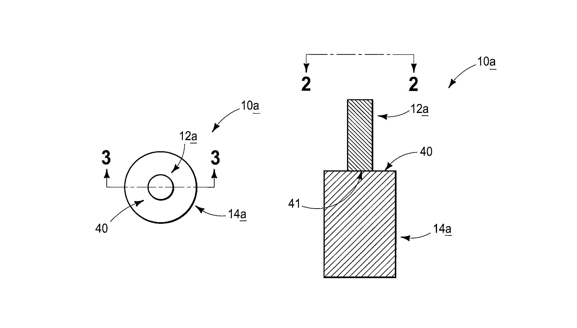
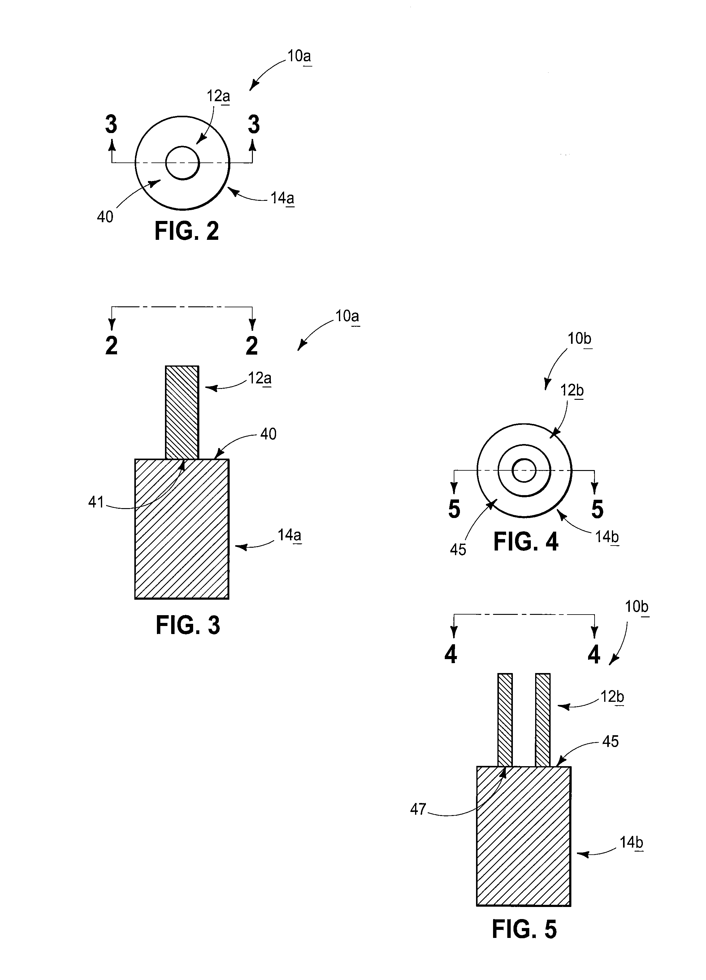
FIGS. 2 and 3 are a top view and a diagrammatic cross-sectional view of an example embodiment fuse. FIG. 3 is along the line 3-3 of FIG. 2, and FIG. 2 is from the orientation shown along the line 2-2 in FIG. 3.
FIGS. 4 and 5 are a top view and a diagrammatic cross-sectional view of an example embodiment fuse. FIG. 5 is along the line 5-5 of FIG. 4, and FIG. 4 is from the orientation shown along the line 4-4 in FIG. 5.
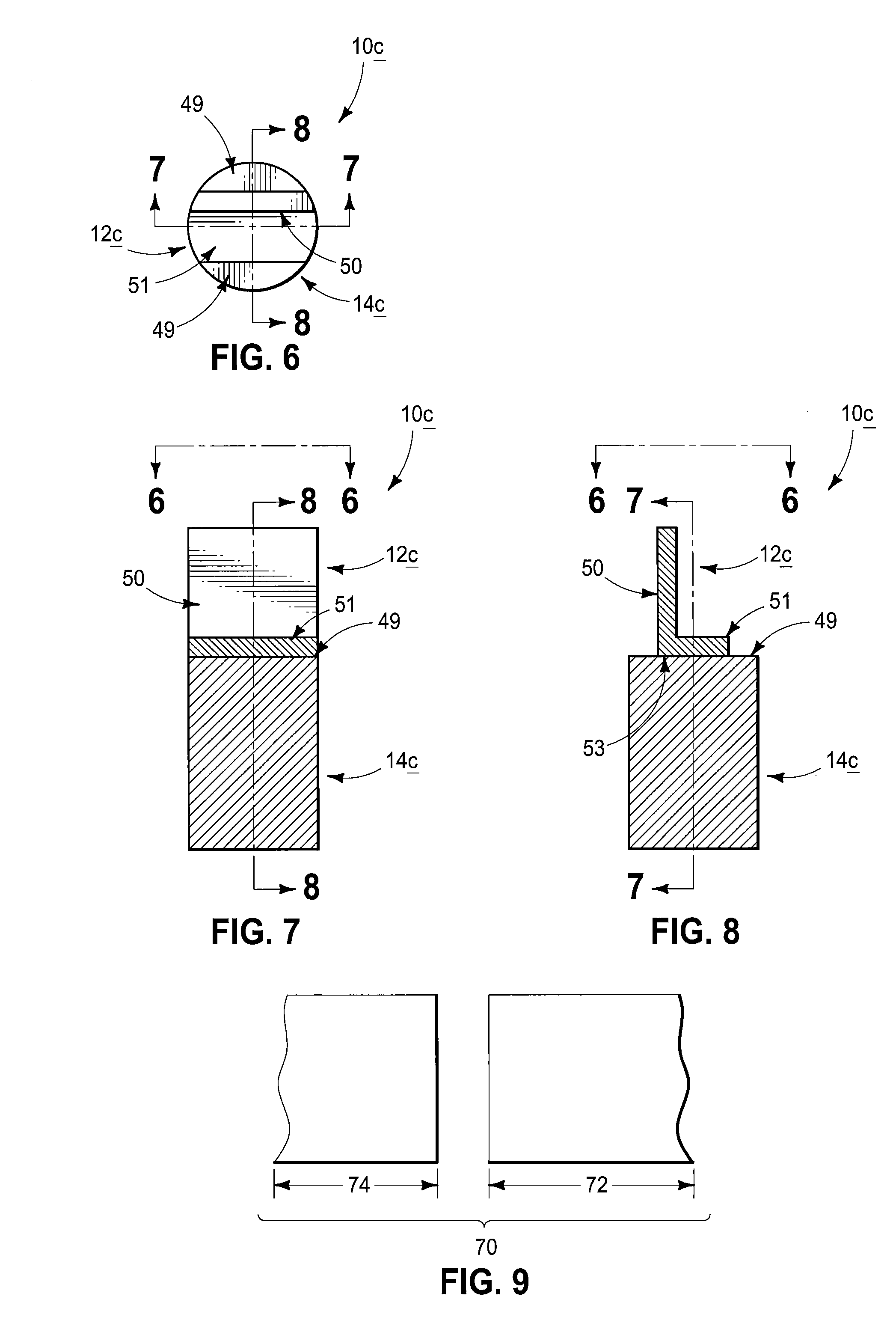
FIGS. 6-8 are a top view and a pair of diagrammatic cross-sectional views of an example embodiment fuse. FIG. 7 is along the lines 7-7 of FIGS. 6 and 8, FIG. 8 is along the lines 8-8 of FIGS. 6 and 7, and FIG. 6 is from the orientation shown along the lines 6-6 in FIGS. 7 and 8.
FIG. 9 diagrammatically illustrates a plan view of a semiconductor construction comprising a fuse region and a memory array region.
DETAILED DESCRIPTION OF THE ILLUSTRATED EMBODIMENTS
In some embodiments, the invention includes fuses formed by providing an electrically conductive structure directly against a tungsten-containing structure. In some embodiments, the electrically conductive structure may be a titanium-containing structure. An interface where the electrically conductive structure joins the tungsten-containing structure is configured to rupture when current through such interface exceeds a predetermined level.
Some embodiments include fuses that may be readily incorporated into existing integrated circuit fabrication. The fuses utilize materials which are already commonly utilized in integrated circuits. For instance, the fuses having titanium-containing structures and tungsten-containing structures may be readily incorporated into existing PCRAM fabrication processes. Specifically, PCRAM already commonly utilizes titanium-containing structures as heaters within memory cells, and already commonly utilizes tungsten-containing structures as conductive interconnects between circuit components.
Example embodiments are described with reference to FIGS. 1-9.
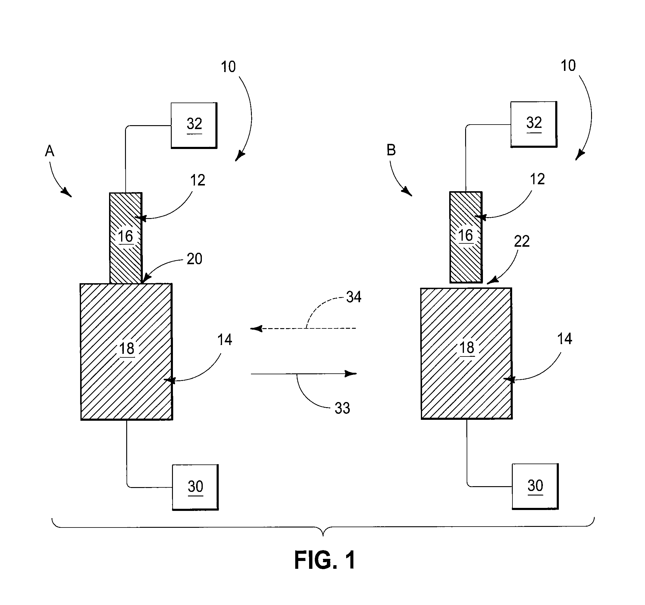
Referring to FIG. 1, a fuse construction 10 is shown in two different operational modes "A" and "B."
The fuse construction comprises an electrically conductive structure 12 over a tungsten-containing structure 14.
The electrically conductive structure 12 may comprise any suitable electrically conductive composition, and in some embodiments may be a titanium-containing structure. The structure 12 comprises a material 16. Such material may be of any suitable composition; and in some embodiments may comprise, consist essentially of, or consist of a mixture of titanium and nitrogen. For instance, the material 16 may comprise, consist essentially of, or consist of titanium nitride; either alone, or in combination with one or more dopants selected from the group consisting of aluminum, silicon and carbon.
The tungsten-containing structure 14 comprises a material 18. Such material may be of any suitable composition; and in some embodiments may comprise, consist essentially of, or consist of tungsten. The tungsten-containing structure may be over a semiconductor base (not shown). Such semiconductor base may comprise silicon, and the tungsten-containing structure may join to the silicon through a tungsten silicide interface (not shown).
If the tungsten-containing structure 14 is over a semiconductor base, the construction 10 may be considered to be comprised by a semiconductor substrate. The terms "semiconductive substrate," "semiconductor construction" and "semiconductor substrate" mean any construction comprising semiconductive material, including, but not limited to, bulk semiconductive materials such as a semiconductive wafer (either alone or in assemblies comprising other materials), and semiconductive material layers (either alone or in assemblies comprising other materials). The term "substrate" refers to any supporting structure, including, but not limited to, the semiconductor substrates described above.
The operational mode "A" has the electrically conductive structure 12 directly against the tungsten-containing structure 14. The structure 12 joins to the tungsten-containing structure 14 at an interface 20. Such interface is configured to rupture when current through the interface exceeds a predetermined level. The amount of current suitable to generate such rupture may depend on, among other things, the composition of tungsten-containing structure 14 along the interface, the composition of structure 12 along the interface, and the area of the interface. Thus, the fuse may be tailored for particular applications by adjusting one or more of the composition of structure 12, the composition of tungsten-containing structure 14, and the area of interface 20.
The amount of current suitable to generate the rupture may also depend on the voltage provided across interface 20, but such voltage may be relatively fixed by operational characteristics of an integrated circuit. Accordingly, the voltage may not be an operational parameter which can be readily modified for tailoring operational performance of the fuse.
The amount of current suitable to rupture the interface will be inversely related to the area of the interface. In some embodiments, it will be desired to have the fuse be readily broken with a current less of than or equal to about 3 milliamps. In such embodiments, the total area of the interface 20 may be less than or equal to about 1500 square nanometers (i.e., nm.sup.2), which can enable the fuse to be broken with a current of less than or equal to about 2.5.times.10.sup.-3 amps under a voltage of less than or equal to about 2 volts. Thus, in some embodiments the predetermined current which ruptures the interface may be less than or equal to about 3 milliamps, and may be, for example, about 2.5 milliamps.
In some embodiments, the electrically conductive structure 12 may comprise titanium nitride doped with one or more of silicon, aluminum and carbon. The amount of current suitable to rupture the interface may be related to the type of dopant and the amount of dopant. Thus, operational characteristics of fuse construction 10 may be tailored, to some extent, through the selection of dopant concentration and type provided within the titanium nitride.
The fuse construction 10 is transitioned from the operational mode "A" to the operational mode "B" by providing sufficient current through interface 20 to rupture such interface and thus form the void 22 shown in the operational mode "B."
The fuse construction 10 is diagrammatically illustrated to be provided between circuitry 30 and circuitry 32. The operational mode "A" may be considered to comprise a closed circuit through fuse construction 10 so that the circuitry 30 is electrically connected to the circuitry 32 through the fuse construction, and the operational mode "B" may be considered to comprise an open circuit through the fuse construction so that the circuitry 30 is no longer connected to the circuitry 32.
In some embodiments, the rupture of the interface 20 of the fuse occurs through a mechanism utilizing electron wind. Specifically, current flow through the interface causes electro-migration wherein momentum of moving electrons causes atoms to move from their original positions, and ultimately causes formation of the void 22. The mechanism is provided herein to assist the reader in understanding the invention, and is not to limit the invention except to the extent, if any, that such mechanism is expressly recited in the claims that follow.
The transition from operational mode "A" to operational mode "B" is diagrammatically illustrated with an arrow 33. Another arrow 34 is shown in dashed-line to indicate that there may be a transition from operational mode "B" back to operational mode "A," which may be utilized to reset the fuse in some embodiments. Specifically, if sufficient voltage is provided across the void 22 in operational mode "B," and if such voltage is provided in an appropriate orientation so that current may be flowed across the void in an opposite direction (i.e., an opposite polarity) to the current flow that created the void, then it may be possible to recover the interface 20 of operational mode "A." In the embodiment discussed above in which the total area of the interface 20 was less than or equal to about 1500 nm.sup.2, the interface could be recovered with a voltage exceeding about 6 volts.
A difficulty in recovering the interfaces of fuse constructions of the type shown in FIG. 1 is that there may be a substantial variability between seemingly identical fuses relative to the amount of voltage required to accomplish such recovery. Another difficulty is that there may be substantial differences between the recovered fuses relative to the current flow across the reestablished interfaces. Regardless of the above-described difficulties, there may be embodiments in which it is advantageous to recover at least some of the fuses utilized in an integrated circuit.
The fuse construction 10 of FIG. 1 may have any suitable configuration. Example configurations are described with reference to FIGS. 3-8.
Referring to FIG. 3, an example configuration 10a is shown in top view (FIG. 2) and cross-sectional side view (FIG. 3). The construction comprises an electrically conductive structure 12a (which may be a titanium-containing structure) configured as a substantially cylindrical pedestal, and comprises a tungsten-containing structure 14a which is also configured to be substantially cylindrical. The tungsten-containing structure 14a has a substantially circular end 40, and the pedestal 12a has an edge 41 which is directly against such end. In the shown embodiment, the edge 41 is a substantially circular end of the pedestal 12a.
In the shown embodiment of FIGS. 2 and 3, the end 40 of the tungsten-containing structure 14a is larger than the end 41 of the structure 12a. In other words, the end 40 has a first total area (i.e., a first surface area), and the end 41 has a second total area (i.e., a second surface area); with the second total area being less than the first total area.
Referring to FIGS. 4 and 5, an example configuration 10b is shown in top view (FIG. 4) and cross-sectional side view (FIG. 5). The construction comprises an electrically conductive structure 12b (which may be a titanium-containing structure) configured as a substantially cylindrical annular structure, and comprises a substantially cylindrical tungsten-containing structure 14b. The tungsten-containing structure 14a has a substantially circular end 45, and the pedestal 12b has an annular edge 47 which is directly against such end. In the shown embodiment, the edge 47 is a substantially circular end of the annular structure 12b.
Referring to FIGS. 6-8, an example configuration 10c is shown in top view (FIG. 6) and in a pair of cross-sectional side views (FIGS. 7 and 8). The construction comprises a substantially cylindrical tungsten-containing structure 14c having a substantially circular end 49. The construction 10c also comprises an electrically conductive structure 12c (which may be a titanium-containing structure) configured to comprise a plate 50 oriented to have an edge 53 directly against the end 49 of the tungsten-containing structure 14c; and to have a ledge 51 along the plate 50 and also along the end 49 of the tungsten-containing structure 14c.
As discussed above, an advantage of the fuse constructions described herein may be that such fuse constructions can be readily incorporated into existing integrated circuit fabrication processes. FIG. 9 illustrates an example integrated circuit 70 which may be configured to utilize fuses of the types described above with reference to FIGS. 1-8. The circuit 70 comprises a memory array region 72 and a fuse region 74 (which may be referred to as a fuse bank). The memory array region may be configured to comprise any of numerous types of memory constructions, either now known or yet to be developed. In some embodiments, the memory array region may comprise PCRAM. Such memory may utilize titanium nitride-containing structures as heaters of individual memory cells, and may utilize tungsten-containing structures as electrical interconnects, in accordance with conventional processing.
The utilization of one or more constructions of the types described above with reference to FIGS. 1-8 may enable one or more components of such fuses to be formed simultaneously with one or more components of the memory. For instance, tungsten-containing structures of the fuses may be formed simultaneously with electrical interconnects of the memory and/or titanium-containing structures of the fuses may be formed simultaneously with heater structures of PCRAM cells. Such may advantageously enable fuses to be incorporated into existing integrated circuitry without addition of materials or masking steps beyond those already utilized in fabrication of the integrated circuitry. Although it may be advantageous for the fuses to be patterned utilizing a common mask as that utilized for forming a memory array in some embodiments, in other embodiments it may be preferred to utilize at least one dedicated mask during fabrication of the fuses (for instance, if it is desired to implant dopant into the fuses which is not utilized in the memory).
Although the embodiment of FIG. 9 refers to the integrated circuitry 72 as being memory, in other embodiments other types of integrated circuitry may be utilized in combination with one or more of the fuse types described above with reference to FIGS. 1-8.
The fuses discussed above may be incorporated into electronic systems. Such electronic systems may be used in, for example, memory modules, device drivers, power modules, communication modems, processor modules, and application-specific modules, and may include multilayer, multichip modules. The electronic systems may be any of a broad range of systems, such as, for example, clocks, televisions, cell phones, personal computers, automobiles, industrial control systems, aircraft, etc.
The particular orientation of the various embodiments in the drawings is for illustrative purposes only, and the embodiments may be rotated relative to the shown orientations in some applications. The description provided herein, and the claims that follow, pertain to any structures that have the described relationships between various features, regardless of whether the structures are in the particular orientation of the drawings, or are rotated relative to such orientation.
The cross-sectional views of the accompanying illustrations only show features within the planes of the cross-sections, and do not show materials behind the planes of the cross-sections in order to simplify the drawings.
When a structure is referred to above as being "on" or "against" another structure, it can be directly on the other structure or intervening structures may also be present. In contrast, when a structure is referred to as being "directly on" or "directly against" another structure, there are no intervening structures present. When a structure is referred to as being "connected" or "coupled" to another structure, it can be directly connected or coupled to the other structure, or intervening structures may be present. In contrast, when a structure is referred to as being "directly connected" or "directly coupled" to another structure, there are no intervening structures present.
Some embodiments include a fuse comprising a tungsten-containing structure and an electrically conductive structure directly contacting the tungsten-containing structure. An interface between the tungsten-containing structure and the electrically conductive structure is configured to rupture when current through said interface exceeds a predetermined level.
Some embodiments include a fuse comprising a tungsten-containing structure having a first end with a first total area, and an electrically conductive structure having a second end with a second total area. The second total area is less than the first total area. An entirety of the second end directly contacts the first end. An interface between the first and second ends is configured to rupture when current through said interface exceeds a predetermined level. The electrically conductive structure may be a titanium-containing structure comprising a mixture containing titanium and nitrogen. The interface comprises an area of less than or equal to about 1500 nm.sup.2.
Some embodiments include a method of forming and using a fuse. A fuse is formed to comprise a tungsten-containing structure directly contacting a titanium-containing structure. An interface between the tungsten-containing structure and the titanium-containing structure is configured to rupture when current through said interface exceeds a predetermined level. Current exceeding the predetermined level is passed through the interface to rupture the interface.
In compliance with the statute, the subject matter disclosed herein has been described in language more or less specific as to structural and methodical features. It is to be understood, however, that the claims are not limited to the specific features shown and described, since the means herein disclosed comprise example embodiments. The claims are thus to be afforded full scope as literally worded, and to be appropriately interpreted in accordance with the doctrine of equivalents.
* * * * *
References
D00000
D00001
D00002
D00003
XML
uspto.report is an independent third-party trademark research tool that is not affiliated, endorsed, or sponsored by the United States Patent and Trademark Office (USPTO) or any other governmental organization. The information provided by uspto.report is based on publicly available data at the time of writing and is intended for informational purposes only.
While we strive to provide accurate and up-to-date information, we do not guarantee the accuracy, completeness, reliability, or suitability of the information displayed on this site. The use of this site is at your own risk. Any reliance you place on such information is therefore strictly at your own risk.
All official trademark data, including owner information, should be verified by visiting the official USPTO website at www.uspto.gov. This site is not intended to replace professional legal advice and should not be used as a substitute for consulting with a legal professional who is knowledgeable about trademark law.