Method for increasing the integration level of superconducting electronics circuits, and a resulting circuit
Yohannes , et al.
U.S. patent number 10,283,694 [Application Number 15/679,935] was granted by the patent office on 2019-05-07 for method for increasing the integration level of superconducting electronics circuits, and a resulting circuit. This patent grant is currently assigned to Hypres, Inc.. The grantee listed for this patent is Hypres, Inc.. Invention is credited to Richard Hunt, Alexander F. Kirichenko, John Vivalda, Daniel Yohannes.


View All Diagrams
| United States Patent | 10,283,694 |
| Yohannes , et al. | May 7, 2019 |
Method for increasing the integration level of superconducting electronics circuits, and a resulting circuit
Abstract
A method for increasing the integration level of superconducting electronic circuits, comprising fabricating a series of planarized electrically conductive layers patterned into wiring, separated by planarized insulating layers, with vias communicating between the conductive layers. Contrary to the standard sequence of patterning from the bottom up, the pattern of vias in at least one insulating layer is formed prior to the pattern of wiring in the underlying conductive layer. This enables a reduction in the number of planarization steps, leading to a fabrication process which is faster and more reliable. In a preferred embodiment, the superconductor is niobium and the insulator is silicon dioxide. This method can provide 10 or more wiring layers in a complex integrated circuit, and is compatible with non-planarized circuits placed above the planarized wiring layers.
| Inventors: | Yohannes; Daniel (Stamford, CT), Kirichenko; Alexander F. (Pleasantville, NY), Vivalda; John (Poughkeepsie, NY), Hunt; Richard (Park Ridge, NJ) | ||||||||||
|---|---|---|---|---|---|---|---|---|---|---|---|
| Applicant: |
|
||||||||||
| Assignee: | Hypres, Inc. (Elmsford,
NY) |
||||||||||
| Family ID: | 52996070 | ||||||||||
| Appl. No.: | 15/679,935 | ||||||||||
| Filed: | August 17, 2017 |
Prior Publication Data
| Document Identifier | Publication Date | |
|---|---|---|
| US 20170345990 A1 | Nov 30, 2017 | |
Related U.S. Patent Documents
| Application Number | Filing Date | Patent Number | Issue Date | ||
|---|---|---|---|---|---|
| 14508514 | Aug 22, 2017 | 9741918 | |||
| 61887919 | Oct 7, 2013 | ||||
| Current U.S. Class: | 1/1 |
| Current CPC Class: | H01L 39/223 (20130101); H01L 39/2493 (20130101); H01L 27/18 (20130101); H01L 39/2406 (20130101); H01L 39/025 (20130101); G11C 11/44 (20130101) |
| Current International Class: | H01L 39/22 (20060101); H01L 27/18 (20060101); H01L 39/24 (20060101); H01L 39/02 (20060101); G11C 11/44 (20060101) |
References Cited [Referenced By]
U.S. Patent Documents
| 4075756 | February 1978 | Kircher et al. |
| 4418095 | November 1983 | Young et al. |
| 4437227 | March 1984 | Flannery et al. |
| 4448800 | May 1984 | Ehara et al. |
| 4456506 | June 1984 | Stein et al. |
| 4486464 | December 1984 | Young |
| 4533624 | August 1985 | Sheppard |
| 4837604 | June 1989 | Faris |
| 4904619 | February 1990 | Yamada et al. |
| 5049543 | September 1991 | Van Der Kolk et al. |
| 5055158 | October 1991 | Gallagher et al. |
| 5059448 | October 1991 | Chandra et al. |
| 5063267 | November 1991 | Hanneman et al. |
| 5091162 | February 1992 | Frye et al. |
| 5104848 | April 1992 | Miedema et al. |
| 5118530 | June 1992 | Hanneman et al. |
| 5173620 | December 1992 | Fujimaki et al. |
| 5229360 | July 1993 | Shiga et al. |
| 5246782 | September 1993 | Kennedy et al. |
| 5246885 | September 1993 | Braren et al. |
| 5256636 | October 1993 | Wellstood et al. |
| 5262201 | October 1993 | Chandra et al. |
| 5276639 | January 1994 | Inoue |
| 5291035 | March 1994 | Wellstood et al. |
| 5298875 | March 1994 | Laibowitz et al. |
| 5322817 | June 1994 | James et al. |
| 5326988 | July 1994 | Ishida |
| 5347086 | September 1994 | Potter et al. |
| 5365476 | November 1994 | Mukhanov |
| 5388068 | February 1995 | Ghoshal et al. |
| 5399546 | March 1995 | Nakamura et al. |
| 5407903 | March 1995 | Nakamura et al. |
| 5409777 | April 1995 | Kennedy et al. |
| 5413982 | April 1995 | Inada et al. |
| 5434127 | July 1995 | Nakamura et al. |
| 5436029 | July 1995 | Ballance et al. |
| 5439875 | August 1995 | Tanaka et al. |
| 5462918 | October 1995 | Nakamura et al. |
| 5462919 | October 1995 | Tanaka et al. |
| 5471069 | November 1995 | Nakamura et al. |
| 5476719 | December 1995 | Sandell et al. |
| 5477061 | December 1995 | Morohashi |
| 5494891 | February 1996 | Nakamura et al. |
| 5506197 | April 1996 | Nakamura et al. |
| 5523686 | June 1996 | Kirtley et al. |
| 5529524 | June 1996 | Jones |
| 5539215 | July 1996 | Nakamura et al. |
| 5548181 | August 1996 | Jones |
| 5565695 | October 1996 | Johnson |
| 5566045 | October 1996 | Summerfelt et al. |
| 5574290 | November 1996 | You |
| 5576928 | November 1996 | Summerfelt et al. |
| 5581436 | December 1996 | Summerfelt et al. |
| 5587623 | December 1996 | Jones |
| 5609925 | March 1997 | Camilletti et al. |
| 5619097 | April 1997 | Jones |
| 5619393 | April 1997 | Summerfelt et al. |
| 5621223 | April 1997 | Nakamura et al. |
| 5625290 | April 1997 | You |
| 5629838 | May 1997 | Knight et al. |
| 5637555 | June 1997 | Nakamura et al. |
| 5689087 | November 1997 | Jack |
| 5710437 | January 1998 | Kurakado et al. |
| 5717222 | February 1998 | Nakamura et al. |
| 5730922 | March 1998 | Babb et al. |
| 5736456 | April 1998 | Akram |
| 5739084 | April 1998 | Nakamura et al. |
| 5742459 | April 1998 | Shen et al. |
| 5750474 | May 1998 | Sung et al. |
| 5753014 | May 1998 | Van Rijn |
| 5764567 | June 1998 | Parkin |
| 5776863 | July 1998 | Silver |
| 5786690 | July 1998 | Kirtley et al. |
| 5789346 | August 1998 | Nakamura et al. |
| 5801393 | September 1998 | Sung et al. |
| 5801984 | September 1998 | Parkin |
| 5818373 | October 1998 | Semenov et al. |
| 5820923 | October 1998 | Ballance et al. |
| 5840204 | November 1998 | Inada et al. |
| 5853808 | December 1998 | Arkles et al. |
| 5854492 | December 1998 | Chinone et al. |
| 5903058 | May 1999 | Akram |
| 5912503 | June 1999 | Chan et al. |
| 5923970 | July 1999 | Kirlin |
| 6016000 | January 2000 | Moslehi |
| 6023072 | February 2000 | Silver |
| 6051440 | April 2000 | Chan et al. |
| 6051846 | April 2000 | Burns et al. |
| 6072689 | June 2000 | Kirlin |
| 6110278 | August 2000 | Saxena |
| 6110392 | August 2000 | Kerber et al. |
| 6124198 | September 2000 | Moslehi |
| 6157329 | December 2000 | Lee et al. |
| 6165801 | December 2000 | Burns et al. |
| 6190998 | February 2001 | Bruel et al. |
| 6191073 | February 2001 | Hojczyk et al. |
| 6285050 | September 2001 | Emma et al. |
| 6306729 | October 2001 | Sakaguchi et al. |
| 6384423 | May 2002 | Kerber et al. |
| 6420251 | July 2002 | Elmadjian et al. |
| 6429095 | August 2002 | Sakaguchi et al. |
| 6517944 | February 2003 | Puzey et al. |
| 6528814 | March 2003 | Frank et al. |
| 6593212 | July 2003 | Kub et al. |
| 6600638 | July 2003 | Gill |
| 6604270 | August 2003 | Kincaid et al. |
| 6623355 | September 2003 | McClain et al. |
| 6624047 | September 2003 | Sakaguchi et al. |
| 6642608 | November 2003 | Hu |
| 6717845 | April 2004 | Saito et al. |
| 6728113 | April 2004 | Knight et al. |
| 6743078 | June 2004 | McClain et al. |
| 6777036 | August 2004 | Bravo Vasquez et al. |
| 6804146 | October 2004 | Johnson |
| 6807090 | October 2004 | Johnson |
| 6807094 | October 2004 | Saito et al. |
| 6809959 | October 2004 | Johnson |
| 6825106 | November 2004 | Gao et al. |
| 6849469 | February 2005 | Thuruthiyil et al. |
| 6852167 | February 2005 | Ahn |
| 6870761 | March 2005 | Johnson |
| 6911665 | June 2005 | Aoyagi et al. |
| 6916719 | July 2005 | Knight et al. |
| 6926921 | August 2005 | Stasiak et al. |
| 6946597 | September 2005 | Sager et al. |
| 6967154 | November 2005 | Meng et al. |
| 6975533 | December 2005 | Johnson |
| 6992344 | January 2006 | Coolbaugh et al. |
| 7019391 | March 2006 | Tran |
| 7042004 | May 2006 | Magnus et al. |
| 7042035 | May 2006 | Rinerson et al. |
| 7050329 | May 2006 | Johnson |
| 7064976 | June 2006 | Johnson |
| 7068535 | June 2006 | Johnson |
| 7081417 | July 2006 | Hinode et al. |
| 7106159 | September 2006 | Delamare et al. |
| 7115218 | October 2006 | Kydd et al. |
| 7129552 | October 2006 | Gao et al. |
| 7142078 | November 2006 | Rostaing et al. |
| 7160577 | January 2007 | Ahn et al. |
| 7161112 | January 2007 | Smith et al. |
| 7166816 | January 2007 | Chen et al. |
| 7215570 | May 2007 | Johnson |
| 7229745 | June 2007 | Lamarre |
| 7235424 | June 2007 | Chen et al. |
| 7259434 | August 2007 | Ahn et al. |
| 7269059 | September 2007 | Morise et al. |
| 7279686 | October 2007 | Schneiker |
| 7279732 | October 2007 | Meng et al. |
| 7311944 | December 2007 | Sambasivan et al. |
| 7319069 | January 2008 | Den et al. |
| 7323348 | January 2008 | Aoyagi et al. |
| 7330369 | February 2008 | Tran |
| 7338907 | March 2008 | Li et al. |
| 7339819 | March 2008 | Johnson |
| 7371698 | May 2008 | Moriya et al. |
| 7375417 | May 2008 | Tran |
| 7393699 | July 2008 | Tran |
| 7396741 | July 2008 | Mund et al. |
| 7397060 | July 2008 | Lung |
| 7410668 | August 2008 | Ahn |
| 7456421 | November 2008 | Lung |
| 7463512 | December 2008 | Lung |
| 7473576 | January 2009 | Lung |
| 7476587 | January 2009 | Lung |
| 7489537 | February 2009 | Tran |
| 7505310 | March 2009 | Nagasawa et al. |
| 7507519 | March 2009 | Toyoda |
| 7510664 | March 2009 | Carr |
| 7514367 | April 2009 | Lung et al. |
| 7527985 | May 2009 | Lai et al. |
| 7534647 | May 2009 | Lung |
| 7535035 | May 2009 | Baek et al. |
| 7541198 | June 2009 | Magnus et al. |
| 7541263 | June 2009 | Moriceau et al. |
| 7541558 | June 2009 | Smith et al. |
| 7554144 | June 2009 | Lai et al. |
| 7554161 | June 2009 | Ahn et al. |
| 7560337 | July 2009 | Ho et al. |
| 7569844 | August 2009 | Lung |
| 7595218 | September 2009 | Ho et al. |
| 7605079 | October 2009 | Lai et al. |
| 7630227 | December 2009 | Tran |
| 7638359 | December 2009 | Lung |
| 7642539 | January 2010 | Lung |
| 7646570 | January 2010 | Gill et al. |
| 7670646 | March 2010 | Ahn et al. |
| 7682868 | March 2010 | Lung |
| 7687938 | March 2010 | Bunyk et al. |
| 7696506 | April 2010 | Lung |
| 7697316 | April 2010 | Lai et al. |
| 7732003 | June 2010 | Toyoda |
| 7732800 | June 2010 | Lai et al. |
| 7741636 | June 2010 | Ho |
| 7749854 | July 2010 | Lung |
| 7755076 | July 2010 | Lung |
| 7759747 | July 2010 | Forbes et al. |
| 7786461 | August 2010 | Lung |
| 7816661 | October 2010 | Lai et al. |
| 7820997 | October 2010 | Lai et al. |
| 7821747 | October 2010 | Gill |
| 7852106 | December 2010 | Herr et al. |
| 7864560 | January 2011 | Tran |
| 7868539 | January 2011 | Ohara |
| 7869221 | January 2011 | Knight et al. |
| 7870087 | January 2011 | Macready et al. |
| 7872291 | January 2011 | Meng et al. |
| 7875493 | January 2011 | Lung |
| 7879645 | February 2011 | Lung et al. |
| 7884342 | February 2011 | Lung |
| 7902038 | March 2011 | Aspar et al. |
| 7932129 | April 2011 | Lung |
| 7956344 | June 2011 | Lung |
| 7972893 | July 2011 | Lai et al. |
| 7984012 | July 2011 | Coury et al. |
| 8003410 | August 2011 | Kerner et al. |
| 8026038 | September 2011 | Ogihara et al. |
| 8032474 | October 2011 | Macready et al. |
| 8039392 | October 2011 | Lai et al. |
| 8055318 | November 2011 | Kadin |
| 8062923 | November 2011 | Lung |
| 8076242 | December 2011 | Kim et al. |
| 8080440 | December 2011 | Lai et al. |
| 8084762 | December 2011 | Tran |
| 8106376 | January 2012 | Lai et al. |
| 8110456 | February 2012 | Lung |
| 8111541 | February 2012 | Lai et al. |
| 8114763 | February 2012 | Forbes et al. |
| 8119020 | February 2012 | Ito et al. |
| 8124426 | February 2012 | Gaidis |
| 8124906 | February 2012 | Holber et al. |
| 8138857 | March 2012 | Ding et al. |
| 8143150 | March 2012 | Jeong |
| 8158963 | April 2012 | Ho et al. |
| 8168291 | May 2012 | Shah et al. |
| 8178388 | May 2012 | Ho |
| 8188563 | May 2012 | Finkelstein et al. |
| 8189980 | May 2012 | Miyazaki et al. |
| 8193878 | June 2012 | Ding et al. |
| 8211833 | July 2012 | Gilbert et al. |
| 8237140 | August 2012 | Lung et al. |
| 8237148 | August 2012 | Lung |
| 8244662 | August 2012 | Coury et al. |
| 8247799 | August 2012 | Bunyk et al. |
| 8253320 | August 2012 | Nakanishi et al. |
| 8301214 | October 2012 | Tolpygo |
| 8324734 | December 2012 | Gaidis |
| 8330357 | December 2012 | Ohara |
| 8339030 | December 2012 | Nakanishi et al. |
| 8362576 | January 2013 | Meng et al. |
| 8383929 | February 2013 | Milshtein et al. |
| 8384060 | February 2013 | Ryoo et al. |
| 8404620 | March 2013 | Gilbert et al. |
| 8437818 | May 2013 | Tolpygo et al. |
| 8450716 | May 2013 | Tran |
| 8476988 | July 2013 | Ding et al. |
| 8508314 | August 2013 | Ding et al. |
| 8513637 | August 2013 | Lung |
| 8536566 | September 2013 | Johansson et al. |
| 8571614 | October 2013 | Mukhanov et al. |
| 8609593 | December 2013 | Gilbert et al. |
| 8653497 | February 2014 | Tran |
| 8759257 | June 2014 | Gilbert et al. |
| 8796181 | August 2014 | Gilbert et al. |
| 2002/0055323 | May 2002 | McClain et al. |
| 2002/0068419 | June 2002 | Sakaguchi et al. |
| 2002/0148560 | October 2002 | Carr |
| 2002/0197415 | December 2002 | Bravo Vasquez et al. |
| 2003/0194953 | October 2003 | McClain et al. |
| 2004/0053079 | March 2004 | Horibe et al. |
| 2004/0056335 | March 2004 | Aoyagi et al. |
| 2004/0061229 | April 2004 | Moslehi |
| 2004/0069991 | April 2004 | Dunn et al. |
| 2004/0071019 | April 2004 | Magnus et al. |
| 2004/0081751 | April 2004 | Nakanishi et al. |
| 2004/0151893 | August 2004 | Kydd et al. |
| 2004/0159869 | August 2004 | Rinerson et al. |
| 2004/0206267 | October 2004 | Sambasivan et al. |
| 2004/0222500 | November 2004 | Aspar et al. |
| 2004/0266209 | December 2004 | Hinode et al. |
| 2005/0002448 | January 2005 | Knight et al. |
| 2005/0042430 | February 2005 | Toyoda |
| 2005/0058840 | March 2005 | Toyoda |
| 2005/0092929 | May 2005 | Schneiker |
| 2005/0121068 | June 2005 | Sager et al. |
| 2005/0123674 | June 2005 | Stasiak et al. |
| 2005/0149002 | July 2005 | Wang et al. |
| 2005/0149169 | July 2005 | Wang et al. |
| 2005/0182482 | August 2005 | Wang et al. |
| 2005/0191763 | September 2005 | Aoyagi et al. |
| 2005/0197254 | September 2005 | Stasiak et al. |
| 2005/0218397 | October 2005 | Tran |
| 2005/0218398 | October 2005 | Tran |
| 2005/0230822 | October 2005 | Tran |
| 2005/0231855 | October 2005 | Tran |
| 2005/0237140 | October 2005 | Rostaing et al. |
| 2005/0240100 | October 2005 | Wang et al. |
| 2005/0244337 | November 2005 | Wang et al. |
| 2005/0261763 | November 2005 | Wang et al. |
| 2005/0267000 | December 2005 | Kerber |
| 2005/0277064 | December 2005 | Lamarre |
| 2005/0278020 | December 2005 | Wang et al. |
| 2006/0030074 | February 2006 | Mund et al. |
| 2006/0073706 | April 2006 | Li et al. |
| 2006/0097288 | May 2006 | Baek et al. |
| 2006/0138394 | June 2006 | Den et al. |
| 2006/0142853 | June 2006 | Wang et al. |
| 2006/0145326 | July 2006 | Tran |
| 2006/0162497 | July 2006 | Kodas et al. |
| 2006/0165898 | July 2006 | Kodas et al. |
| 2006/0165910 | July 2006 | Kodas et al. |
| 2006/0166057 | July 2006 | Kodas et al. |
| 2006/0255987 | November 2006 | Nagasawa et al. |
| 2006/0260674 | November 2006 | Tran |
| 2006/0264069 | November 2006 | Magnus et al. |
| 2006/0270082 | November 2006 | Moriya et al. |
| 2006/0284158 | December 2006 | Lung et al. |
| 2006/0286743 | December 2006 | Lung et al. |
| 2007/0108429 | May 2007 | Lung |
| 2007/0131922 | June 2007 | Lung |
| 2007/0138458 | June 2007 | Lung |
| 2007/0155172 | July 2007 | Lai et al. |
| 2007/0158690 | July 2007 | Ho et al. |
| 2007/0161186 | July 2007 | Ho |
| 2007/0173019 | July 2007 | Ho et al. |
| 2007/0176261 | August 2007 | Lung |
| 2007/0194225 | August 2007 | Zorn |
| 2007/0241371 | October 2007 | Lai et al. |
| 2007/0259528 | November 2007 | Moriceau et al. |
| 2007/0278529 | December 2007 | Lai et al. |
| 2007/0281420 | December 2007 | Lai et al. |
| 2007/0285843 | December 2007 | Tran |
| 2007/0298535 | December 2007 | Lung |
| 2008/0023442 | January 2008 | Ito et al. |
| 2008/0060947 | March 2008 | Kitsuka et al. |
| 2008/0096341 | April 2008 | Lai et al. |
| 2008/0106923 | May 2008 | Lung |
| 2008/0116449 | May 2008 | Macready et al. |
| 2008/0135824 | June 2008 | Lai et al. |
| 2008/0138929 | June 2008 | Lung |
| 2008/0138930 | June 2008 | Lung |
| 2008/0138931 | June 2008 | Lung |
| 2008/0150422 | June 2008 | Ohara |
| 2008/0173931 | July 2008 | Ho et al. |
| 2008/0192534 | August 2008 | Lung |
| 2008/0203375 | August 2008 | Lung |
| 2008/0217648 | September 2008 | Ohara |
| 2008/0218519 | September 2008 | Coury et al. |
| 2008/0239791 | October 2008 | Tran |
| 2008/0246014 | October 2008 | Lung |
| 2008/0247224 | October 2008 | Lung |
| 2008/0258126 | October 2008 | Lung |
| 2008/0259672 | October 2008 | Lung |
| 2008/0266940 | October 2008 | Lai et al. |
| 2008/0277766 | November 2008 | Cantor et al. |
| 2008/0315978 | December 2008 | Knight et al. |
| 2009/0008632 | January 2009 | Bunyk et al. |
| 2009/0014706 | January 2009 | Lung |
| 2009/0032796 | February 2009 | Lung |
| 2009/0042335 | February 2009 | Lung |
| 2009/0079494 | March 2009 | Kerner et al. |
| 2009/0098716 | April 2009 | Lung |
| 2009/0101883 | April 2009 | Lai et al. |
| 2009/0102369 | April 2009 | Nakanishi et al. |
| 2009/0104771 | April 2009 | Lung |
| 2009/0116277 | May 2009 | Tran |
| 2009/0189138 | July 2009 | Lung et al. |
| 2009/0230376 | September 2009 | Ryoo et al. |
| 2009/0230378 | September 2009 | Ryoo et al. |
| 2009/0236743 | September 2009 | Ho et al. |
| 2009/0239358 | September 2009 | Lai et al. |
| 2009/0295510 | December 2009 | Miyazaki et al. |
| 2010/0012167 | January 2010 | Milshtein et al. |
| 2010/0012353 | January 2010 | Milshtein et al. |
| 2010/0068878 | March 2010 | Lung |
| 2010/0073995 | March 2010 | Tran |
| 2010/0133514 | June 2010 | Bunyk et al. |
| 2010/0178825 | July 2010 | Shah et al. |
| 2010/0207095 | August 2010 | Lai et al. |
| 2010/0216279 | August 2010 | Lai et al. |
| 2010/0221888 | September 2010 | Ho |
| 2010/0237316 | September 2010 | Lung |
| 2010/0279000 | November 2010 | Sambasivan et al. |
| 2010/0297824 | November 2010 | Lung |
| 2011/0012084 | January 2011 | Lai et al. |
| 2011/0024409 | February 2011 | Shah et al. |
| 2011/0057169 | March 2011 | Harris et al. |
| 2011/0060711 | March 2011 | Macready et al. |
| 2011/0076825 | March 2011 | Lung |
| 2011/0079817 | April 2011 | Ohara |
| 2011/0089405 | April 2011 | Ladizinsky et al. |
| 2011/0110141 | May 2011 | Tran |
| 2011/0124483 | May 2011 | Shah et al. |
| 2011/0136282 | June 2011 | Shirasawa et al. |
| 2011/0163455 | July 2011 | Gaidis |
| 2011/0168089 | July 2011 | Shah et al. |
| 2011/0174519 | July 2011 | Shah et al. |
| 2011/0186775 | August 2011 | Shah et al. |
| 2011/0207289 | August 2011 | Jeong |
| 2011/0238607 | September 2011 | Coury et al. |
| 2012/0000691 | January 2012 | Shah et al. |
| 2012/0012833 | January 2012 | Shirasawa et al. |
| 2012/0012870 | January 2012 | Nakanishi et al. |
| 2012/0012897 | January 2012 | Besser et al. |
| 2012/0091429 | April 2012 | Tran |
| 2012/0133050 | May 2012 | Gaidis |
| 2012/0164429 | June 2012 | Shah et al. |
| 2012/0263935 | October 2012 | Ledford et al. |
| 2012/0299175 | November 2012 | Tran |
| 2013/0043452 | February 2013 | Meyer et al. |
| 2013/0076231 | March 2013 | Nakanishi et al. |
| 2013/0082232 | April 2013 | Wu et al. |
| 2013/0083443 | April 2013 | Edwards |
| 2013/0096825 | April 2013 | Mohanty |
| 2013/0163310 | June 2013 | Tran |
| 2013/0196856 | August 2013 | Li et al. |
| 2013/0200429 | August 2013 | Pan |
| 2013/0313526 | November 2013 | Harris et al. |
| 2014/0126269 | May 2014 | Tran |
Other References
|
Tetsuro Satoh, "Planarization Process for Fabricating Multi-Layer Nb Integrated Circuits Incorporating Top Active Layer", Vol. 19, No. 3, Jun. 2009, p. 1-4 (Year: 2009). cited by examiner . Sergey Tolpygo, "Deep sub-micron stud-via technology for superconducting VLSI Circuits" Lincoln Laboratory, Sep. 2013, pp. 1-13 (Year: 2013). cited by examiner . Tolpygo, Sergey K., et al. "Deep sub-micron stud-via technology of superconductor VLSI circuits." Superconductor Science and Technology 27.2 (2014): 025016. cited by applicant . Tolpygo, Sergey K., et al. "Fabrication Process and Properties of Fully-Planarized Deep-Submicron Nb/Al--AlOx/Nb Josephson Junctions for VLSI Circuits." arXiv preprint arXiv:1408.5829 (2014). cited by applicant . Tolpygo, Sergey K., et al. "20 Process Development for Superconducting Integrated Circuits With 80 GHz Clock Frequency." Applied Superconductivity, IEEE Transactions on 17.2 (2007): 946-951. cited by applicant . Silver, A., et al. "Development of superconductor electronics technology for high-end computing." Superconductor Science and Technology 16.12 (2003): 1368. cited by applicant . Satoh, Tetsuro, et al. "Fabrication process of planarized multi-layer Nb integrated circuits." Applied Superconductivity, IEEE Transactions on 15.2 (2005): 78-81. cited by applicant . Numata, Hideaki et al, "Fabrication Technology for Nb Integrated Circuits," LEICE Trans. Electron, vol. E84-C, No. 1, Jan. 2001. cited by applicant . Nagasawa, S., et al. "Development of advanced Nb process for SFQ circuits." Physica C: Superconductivity 412 (2004): 1429-1436. cited by applicant . Nagasawa, Shuichi, et al. "Planarized multi-layer fabrication technology for LTS large-scale SFQ circuits." Superconductor Science and Technology 16.12 (2003): 1483. cited by applicant . Nagasawa, S., et al. "New Nb multi-layer fabrication process for large-scale SFQ circuits." Physica C: Superconductivity 469.15 (2009): 1578-1584. cited by applicant . Mitamura, Naoki, et al. "Suppression of Magnetic Flux Trapping by Moats formed in NbN Ground Planes." Applied physics express 4.1 (2011): 013102. cited by applicant . Ketchen, M. B., et al. "Sub-.mu.m, planarized, Nb--AlOx--Nb Josephson process for 125 mm wafers developed in partnership with Si technology." Applied physics letters 59.20 (1991): 2609-2611. cited by applicant . Hidaka, Mutsuo, et al. "Improvements in fabrication process for Nb-based single flux quantum circuits in Japan." IEICE transactions on electronics 91.3 (2008): 318-324. cited by applicant . Imamura, Takeshi, Tetsuyoshi Shiota, and Shinya Hasuo. "Fabrication of high quality Nb/AlO/sub x/-Al/Nb Josephson junctions. I. Sputtered Nb films for junction electrodes." Applied Superconductivity, IEEE Transactions on 2.1 (1992): 1-14. cited by applicant . Bunyk, Paul, Konstantin Likharev, and Dmitry Zinoviev. "RSFQ technology: Physics and devices." International journal of high speed electronics and systems 11.01 (2001): 257-305. cited by applicant . Likharev, Konstantin K., and Vasilii K. Semenov. "RSFQ logic/memory family: A new Josephson-junction technology for sub-terahertz-clock-frequency digital systems." Applied Superconductivity, IEEE Transactions on 1.1 (1991): 3-28. cited by applicant . Kirichenko, Alex F., et al. "Demonstration of an 8.times.8-bit RSFQ multi-port register file." Superconductive Electronics Conference (ISEC), 2013 IEEE 14th International. IEEE, 2013. cited by applicant . Gopel, Wolfgang, and Klaus Dieter Schierbaum. "SnO< sub> 2</sub> sensors: current status and future prospects." Sensors and Actuators B: Chemical 26.1 (1995): 1-12. cited by applicant . Hulteen, John C., and Richard P. Van Duyne. "Nanosphere lithography: a materials general fabrication process for periodic particle array surfaces" Journal of Vacuum Science & Technology A 13.3 (1995): 1553-1558. cited by applicant . Brock, Darren et al, "Retargeting RSFQ Cells to a Submicron Fabrication Process," IEEE Transactions on Applied Superconductivity, vol. 11, No. 1, Mar. 2001. cited by applicant . Abelson, Lynn A., and George L. Kerber. "Superconductor integrated circuit fabrication technology." Proceedings of the IEEE 92.10 (2004): 1517-1533. cited by applicant . Chen, W., et al. "Rapid single flux quantum T-flip flop operating up to 770 GHz." Applied Superconductivity, IEEE Transactions on 9.2 (1999): 3212-3215. cited by applicant . Tolpygo, Sergey K., et al. "Inductance of circuit structures for MIT LL superconductor electronics fabrication process with 8 niobium layers." Applied Superconductivity, IEEE Transactions on 25.3 (2015): 1-5. cited by applicant . Yohannes, Daniel T., et al. "Planarized, extendible, multilayer fabrication process for superconducting electronics." Applied Superconductivity, IEEE Transactions on 25.3 (2015): 1-5. cited by applicant . Tolpygo, Sergey K., et al. "Fabrication Process and Properties of Fully-Planarized Deep-Submicron Nb/Al-Josephson Junctions for VLSI Circuits." Applied Superconductivity, IEEE Transactions on 25.3 (2015): 1-12. cited by applicant . Ortlep, T. "Recent progress in superconductive digital electronics part II--Japanese contributions." IEEE/CSC & ESAS European Superconductivity News Forum. No. 5. 2008. cited by applicant . Satoh, Tetsuro. "Superconductivity Web21." Feb. 2014, Published by International Superconductivity Technology Center KSP, Kawasaki, Kanagawa 213-0012 Japan. cited by applicant . Luo, W. A., et al. "Two-layer, planar, superconducting multichip module technology." SPIE proceedings series. Society of Photo-Optical Instrumentation Engineers, 2000. cited by applicant . Gallagher, William J., Erik P. Harris, and Mark B. Ketchen. "Superconductivity at IBM--a Centenial Review: Part I--Superconducting Computer and Device Applications." (2012). cited by applicant . Khapaev, Mikhail M. "3D- LS .COPYRGT. Software package for inductance calculation in multilayer superconducting integrated circuits Mikhail M. Khapaev, Anna Yu. Kidiyarova-Shevchenko, Per Magnelind, Mikhail Yu. Kupriyanov Abstract--A new software package 3D-MLSI was devel." cited by applicant . Mattauch, R. J., W. L. Bishop, and A. W. Lichtenberger. "Recent results on: Surface-channel Schottky, InGaAs Schottky, and Nb based SIS mixer element research." Proc. First Int. Symp. Space THz. Technology. 1990. cited by applicant . Beasley, Malcolm R., and Richard W. Ralston. "Electronic Applications of Superconductivity in Japan." International Technology Research Institute, World Technology (WTEC) Division (1998). cited by applicant. |
Primary Examiner: Armand; Marc Anthony
Assistant Examiner: Brasfield; Quinton A
Attorney, Agent or Firm: Tully Rinckey PLLC Hoffberg; Steven M.
Parent Case Text
CROSS REFERENCE TO RELATED APPLICATIONS
The present application is Division of U.S. patent application Ser. No. 14/508,514, filed Oct. 7, 2014, now U.S. Pat. No. 9,741,918, issued Aug. 22, 2017, which is a non-provisional of, and claims benefit of priority under 35 U.S.C. .sctn. 119(e) from, U.S. Provisional Patent Application No. 61/887,919, filed Oct. 7, 2013, each of which is expressly incorporated herein by reference in their entirety.
Claims
What is claimed is:
1. A method of forming a planarized integrated circuit on a substrate, comprising a series of successive planarized layers, comprising: defining a first layer, comprising a first electrically conductive layer, and a second electrically conductive layer on the first electrically conductive layer, by: patterning the second electrically conductive layer into a first set of solid vias extending vertically above the first electrically conductive layer, and the first electrically conductive layer into a first set of wires; depositing a first dielectric over the patterned the first set of solid vias and the first set of wires; etching the deposited first dielectric to produce first Caldera edges over tops of the first set of solid vias as well as dummy patterns over other regions, to create a raised pattern of edges, to permit chemical mechanical polishing in a manner controlled independent of a pattern of the first set of solid vias; and planarizing the first Caldera edges and the dummy patterns using chemical mechanical polishing to expose the tops of the first set of solid vias surrounded by the first dielectric; defining a second layer, comprising a third electrically conductive layer, and a fourth electrically conductive layer on the third electrically conductive layer, by: patterning the fourth electrically conductive layer into a second set of solid vias extending vertically above the third electrically conductive layer, and the third electrically conductive layer into a second set of wires, wherein at least a portion of the second set of solid vias are stacked over a portion of the first set of solid vias to provide a vertically conductive pathway having uniform solid via sizes in the first layer and the second layer; depositing a second dielectric over the patterned the second set of solid vias and the second set of wires; etching the deposited second dielectric to produce at least second Caldera edges over tops of the second set of solid vias; and planarizing the second Caldera edges to expose the tops of the set of solid vias surrounded by dielectric.
2. The method according to claim 1, further comprising depositing an etch stop layer between the first electrically conductive layer and second electrically conductive layer.
3. The method according to claim 2, wherein the second electrically conductive layer is patterned into the first set of solid vias before the first electrically conductive layer is patterned into the first set of wires.
4. The method according to claim 1, wherein the first electrically conductive layer and second electrically conductive layer are in direct contact.
5. The method according to claim 4, wherein the first electrically conductive layer is patterned into the first set of wires before the second electrically conductive layer is deposited.
6. A method of forming a planarized integrated circuit on a substrate, comprising: providing a stack of at least two planarized layers, formed successively on the substrate, each respective layer comprising: a first electrically conductive layer, patterned into a set of solid via plugs which define a set of solid vertically extending structures which electrically interconnect with conductive structures of an adjacent overlying layer; a second electrically conductive layer, patterned into a set of wires by removal of portions of the electrically conductive layer surrounding the set of wires, with the set of solid vertically extending structures extending above the set of wires, wherein at least a portion of the set of wires of one layer is in electrical contact with a portion of the set of solid via plugs of a preceding layer, and having a portion of the set of solid via plugs of the one layer overlying a portion of the set of solid via plugs of the preceding layer; depositing a dielectric layer over the set of solid via plugs and the set of wires; patterning the dielectric layer by an anisotropic etch process etching, to provide a nonplanar raised Caldera pattern surrounding edges of the set of via plugs and a dummy pattern of raised edges over other regions; chemical mechanical polishing the nonplanar raised Caldera pattern surrounding edges of the set of via plugs and the dummy pattern of raised edges over other regions to planarize the respective layer, with upper surfaces of the set of solid via plugs exposed, wherein the nonplanar raised Caldera pattern surrounding edges of the set of via plugs and the dummy pattern of raised edges over other regions permit the chemical mechanical polishing to proceed in a manner controlled independent of a pattern of the set of solid via plugs.
7. The method according to claim 6, wherein the raised Caldera pattern is formed by a complementary-to-the-metal-mask pattern mask biased for misalignment compensation, and reactive ion etching.
8. The method according to claim 6, wherein the first electrically conductive layer and the second first electrically conductive layer each comprise a niobium-based superconductive material.
9. The method according to claim 6, wherein the dielectric layer comprises silicon dioxide.
10. The method according to claim 6, further comprising at least one non-planarized layer lying above the stack of the at least two planarized layers.
11. The method according to claim 6, further comprising at least one Josephson junction formed within a respective planarized layer, electrically connected to the set of wires, configured as part of a single-flux-quantum circuit.
12. The method according to claim 6, wherein a minimum transverse dimension of the set of wires is less than 1 micron.
13. The method according to claim 6, wherein stack of at least two planarized layers comprises a stack of at least ten planarized layers.
14. The method according to claim 6, wherein the at least one electrically conductive layer is formed by plasma-enhanced, chemical vapor deposition.
15. The method according to claim 6, wherein at least one electrically conductive layer is formed by sputtering.
16. The method according to claim 6, wherein at least one electrically conductive layer is patterned by reactive ion etching.
17. A method of forming a planarized integrated circuit on a substrate, comprising a series of successive planarized layers, comprising: forming an electrically conductive wiring layer; forming an electrically conductive via layer; patterning the electrically conductive via layer into a set of solid vias; after patterning the electrically conductive via layer, patterning the electrically conductive wiring layer into a set of wires, wherein portions where the set of solid vias coincide in a plane of the planarized layer with the set of wires define vertically extending conductive solid structures configured to provide a conductive path between the set of wires of the respective layer and a set of wires of an adjacent layer; forming an insulating layer surrounding the set of wires and the set of vias; etching the insulating layer to produce first Caldera edges over tops of the set of vias as well as dummy patterns over other regions, to create a raised pattern of edges, to permit chemical mechanical polishing in a manner controlled independent of a pattern of the set of vias; and planarizing the Caldera edges and the dummy patterns of the insulating layer using chemical mechanical polishing, such that portions of the tops of the vertically extending solid structures are exposed surrounded by the planarized insulating layer substantially dependence on the pattern of the set of vias, and the set of wires is covered.
18. The method to claim 17, further comprising depositing the electrically conductive wiring layer on a planarized surface of a preceding layer, forming an etch stop layer on the electrically conductive wiring layer, and forming the electrically conductive via layer over the etch stop layer, wherein the electrically conductive via layer is initially patterned to expose the etch stop layer surrounding the set of vias, and the portions of the etch stop layer and electrically conductive wiring layer surrounding the set of wires are subsequently removed, such that the set of solid vias comprise the vertically extending solid structures.
19. The method circuit of claim 17, wherein the electrically conductive wiring layer and the electrically conductive via layer are each formed of a cryogenically superconductive material, and the etch stop layer is formed of a material susceptible to induced superconductivity by proximity to the cryogenically superconductive material at cryogenic temperatures.
20. The method of claim 17, wherein the dummy patterns comprise a pattern of narrow peaks extending above a remainder of the insulating layer.
Description
BACKGROUND OF THE INVENTION
Superconducting integrated circuits (ICs) based on Josephson junctions (JJs) are capable of operation with very low power and high speed, orders of magnitude beyond those possible using conventional semiconducting circuits. Recently, superconducting single flux quantum (SFQ) circuits have progressed to even lower power versions with zero-static power dissipation (Mukhanov, U.S. Pat. No. 8,571,614; Herr, U.S. Pat. No. 7,852,106), making them highly competitive for application in next generation energy-efficient computing systems. However, the practical realization of superconducting digital circuits for high-end computing requires a significant increase in circuit complexity and gate density. Conventional SFQ integrated circuit fabrication technology has been proven to deliver SFQ digital ICs with more than 10,000 JJs per die, using a fabrication process with just 4 superconducting niobium (Nb) layers and relatively coarse (1.0 .mu.m) lithography with 1.5-2 .mu.m minimum JJ size, without layer planarization. Further increase in integration density and scale of superconducting ICs requires finer lithography to reduce the size of all circuit components including JJs, vias, thin-film inductors, thin-film resistors, and interconnects. Note that this is a different application than superconducting quantum computing based on similar JJs, for which the required circuit complexity is significantly less, but the operating temperature is much lower (see, e.g., Ladizinsky, US20110089405).
The biggest gain in the IC integration scale can be achieved by adding more superconducting layers using layer planarization, which becomes essential to avoid problems associated with lines over edges. Hinode (U.S. Pat. No. 7,081,417) has demonstrated up to 10 Nb layers with submicron JJ size using planarization based on chemical mechanical polishing (CMP). CMP is generally the rate-limiting step in the overall process, and can also lead to contamination, given that it is a wet process that may generate particulate residues. Another known problem with CMP is that the layer planarization rate may depend on the detailed pattern and scale of the devices in a given layer, and may therefore vary within a layer and between layers. One solution to this problem is to incorporate standard dummy patterns in sparsely populated regions (see, e.g., Chen, U.S. Pat. No. 7,235,424). In contrast, Hinode developed a process without such dummy patterns, but using an inverted mask and etching to create a narrow standard "Caldera" (or crater edge) at all edges. Overall, this creates structures that are largely independent of pattern and scale, permitting control and uniformity of the CMP process.
In order to obtain the greatest increase in circuit density by adding superconducting layers, one needs stackable vias (or plugs) allowing connection between multiple metal layers with minimal parasitic inductance, while not compromising circuit area. This has been a difficult problem requiring the development of special fabrication techniques (e.g., Tolpygo, U.S. Pat. Nos. 8,301,214; 8,437,818).
In general, any fully planarized process requires one step of planarization (using, e.g., CMP) for each patternable layer. For example, consider a basic wiring bi-layer such as that shown in FIG. 25A, comprising a lower wiring layer and an upper insulating layer. The insulating layer must contain holes which are penetrated by conducting vias that can connect the lower wiring layer to other wiring layers above. A standard planarized process would comprise first patterning the metals and insulators in the bottom wiring layer, followed by a first planarization step leading to the intermediate structure in FIG. 25B. This would be followed by depositing and patterning the insulator and metal in the top insulator/via layer, followed by a second planarization step.
The art fails to provide a multi-layer planarization process that requires only a single step of chemical mechanical polishing for each wiring bi-layer.
Planarized superconducting circuit technology is discussed in: Tolpygo, Sergey K., et al. "System and method for providing multi-conductive layer metallic interconnects for superconducting integrated circuits." U.S. Pat. No. 8,437,818. 7 May 2013. Tolpygo, Sergey K., et al. "Deep Sub-Micron Stud-Via Technology for Superconductor VLSI Circuits." arXiv preprint arXiv: 1309.7505 (2013). Kirichenko, Alex F., et al. "Demonstration of an 8.times.8-bit RSFQ multi-port register file." Superconductive Electronics Conference (ISEC), 2013 IEEE 14th International. IEEE, 2013. Berggren, Karl K., et al. "Low T.sub.c superconductive circuits fabricated on 150-mm-diameter wafers using a doubly planarized Nb/AlO.sub.x/Nb process." Applied Superconductivity, IEEE Transactions on 9.2 (1999): 3271-3274. Satoh, Tetsuro, et al. "Fabrication process of planarized multi-layer Nb integrated circuits." Applied Superconductivity, IEEE Transactions on 15.2 (2005): 78-81. Ketchen, M. B., et al. "Sub-.mu.m, planarized, Nb--AlO x-Nb Josephson process for 125 mm wafers developed in partnership with Si technology." Applied physics letters 59.20 (1991): 2609-2611. Nagasawa, S., et al. "Development of advanced Nb process for SFQ circuits." Physica C: Superconductivity 412 (2004): 1429-1436. Nagasawa, S., et al. "New Nb multi-layer fabrication process for large-scale SFQ circuits." Physica C: Superconductivity 469.15 (2009): 1578-1584. Nagasawa, Shuichi, et al. "Planarized multi-layer fabrication technology for LTS large-scale SFQ circuits." Superconductor Science and Technology 16.12 (2003): 1483. Abelson, Lynn A., and George L. Kerber. "Superconductor integrated circuit fabrication technology." Proceedings of the IEEE 92.10 (2004): 1517-1533. Patel, Vijay, and J. E. Lukens. "Self-shunted Nb/AlO.sub.x/Nb Josephson junctions." Applied Superconductivity, IEEE Transactions on 9.2 (1999): 3247-3250. Hidaka, M., et al. "Current status and future prospect of the Nb-based fabrication process for single flux quantum circuits." Superconductor Science and Technology 19.3 (2006): S138. Sauvageau, J. E., et al. "Superconducting integrated circuit fabrication with low temperature ECR-based PECVD SiO.sub.2 dielectric films." Applied Superconductivity, IEEE Transactions on 5.2 (1995): 2303-2309. Castellano, Maria Gabriella, et al. "Characterization of a fabrication process for the integration of superconducting qubits and rapid-single-flux-quantum circuits." Superconductor Science and Technology 19.8 (2006): 860. Okanoue, K. U. M. I., and K. Hamasaki. "Temperature dependence of the return current in BiSrCaCuO stacks fabricated by self-planarizing process." Applied Physics Letters 87 (2005): 252506. Ketchen, M., et al. "Octagonal washer DC SQUIDs and integrated susceptometers fabricated in a planarized sub-.mu.m Nb--AlO.sub.x--Nb technology." Applied Superconductivity, IEEE Transactions on 3.1 (1993): 1795-1799. Hidaka, Mutsuo, et al. "Improvements in fabrication process for Nb-based single flux quantum circuits in Japan." IEICE transactions on electronics 91.3 (2008): 318-324. Brock, Darren K., et al. "Retargeting RSFQ cells to a submicron fabrication process." Applied Superconductivity, IEEE Transactions on 11.1 (2001): 369-372. Tahara, Shuichi, et al. "Superconducting digital electronics." Applied Superconductivity, IEEE Transactions on 11.1 (2001): 463-468. Tolpygo, Sergey K., et al. "20 kA/cm.sup.2 process development for superconducting integrated circuits with 80 GHz clock frequency." IEEE Trans. Appl. Supercond 17.2 (2007): 946-951. Bao, Z., et al. "Fabrication of high quality, deep-submicron Nb/AlO.sub.x/Nb Josephson junctions using chemical mechanical polishing." Applied Superconductivity, IEEE Transactions on 5.2 (1995): 2731-2734. Bhushan, M., R. Rouse, and J. E. Lukens. "Chemical-Mechanical Polishing in Semidirect Contact Mode." Journal of the Electrochemical Society 142.11 (1995): 3845-3851. Lichtenberger, A. W., et al. "Fabrication of micron size Nb/Al-Al.sub.2O.sub.3/Nb junctions with a trilevel resist liftoff process." Magnetics, IEEE Transactions on 27.2 (1991): 3168-3171. LeDuc, H. G., et al. "Submicron area NbN/MgO/NbN tunnel junctions for SIS mixer applications." Magnetics, IEEE Transactions on 27.2 (1991): 3192-3195. Satoh, Tetsuro, et al. "Improvement of Fabrication Process for 10-kA/cm.sup.2 Multi-Layer Nb Integrated Circuits" Applied Superconductivity, IEEE Transactions on 17.2 (2007): 169-172. Bhushan, M., and E. M. Macedo. "Nb/AlO x/Nb trilayer process for the fabrication of submicron Josephson junctions and low-noise dc SQUIDs." Applied physics letters 58.12 (1991): 1323-1325. Silver, A., et al. "Development of superconductor electronics technology for high-end computing." Superconductor Science and Technology 16.12 (2003): 1368. Akaike, H., et al. "Demonstration of a 120 GHz single-flux-quantum shift register circuit based on a 10 kA cm.sup.-2 Nb process." Superconductor Science and Technology 19.5 (2006): S320. Akaike, H., et al. "Design of single flux quantum cells for a 10-Nb-layer process." Physica C: Superconductivity 469.15 (2009): 1670-1673. Numata, Hideaki, and Shuichi Tahara. "Fabrication technology for Nb integrated circuits." IEICE transactions on electronics 84.1 (2001): 2-8. Dmitriev, Pavel N., et al. "High quality Nb-based tunnel junctions for high frequency and digital applications." Applied Superconductivity, IEEE Transactions on 13.2 (2003): 107-110. Chen, W., et al. "Rapid single flux quantum T-flip flop operating up to 770 GHz." Applied Superconductivity, IEEE Transactions on 9.2 (1999): 3212-3215. Numata, Hideaki, et al. "Fabrication technology for high-density Josephson integrated circuits using mechanical polishing planarization." Applied Superconductivity, IEEE Transactions on 9.2 (1999): 3198-3201. Bunyk, P. I., et al. "High-speed single-flux-quantum circuit using planarized niobium-trilayer Josephson junction technology." Applied physics letters 66.5 (1995): 646-648. Gallagher, William J., et al. "Planarization of Josephson integrated circuit." U.S. Pat. No. 5,055,158. 8 Oct. 1991. Dolata, R., et al. "Single-charge devices with ultrasmall Nb/AlO/Nb trilayer Josephson junctions." Journal of applied physics 97 (2005): 054501. Abelson, Lynn A., et al. "Superconductive multi-chip module process for high speed digital applications." Applied Superconductivity, IEEE Transactions on 7.2 (1997): 2627-2630. Chen, Wei, Vijay Patel, and James E. Lukens. "Fabrication of high-quality Josephson junctions for quantum computation using a self-aligned process." Microelectronic engineering 73 (2004): 767-772. Hidaka, M.; Nagasawa, S.; Hinode, K.; Satoh, T. "Device Yield in Nb-Nine-Layer Circuit Fabrication Process", Applied Superconductivity, IEEE Transactions on, On page(s): 1100906-1100906 Volume: 23, Issue: 3, June 2013. Satoh, T.; Hinode, K.; Nagasawa, S.; Kitagawa, Y.; Hidaka, M.; Yoshikawa, N.; Akaike, H.; Fujimaki, A.; Takagi, K.; Takagi, N. "Planarization Process for Fabricating Multi-Layer Nb Integrated Circuits Incorporating Top Active Layer", Applied Superconductivity, IEEE Transactions on, On page(s): 167-170 Volume: 19, Issue: 3, June 2009 Kunert, J.; Brandel, O.; Linzen, S.; Wetzstein, O.; Toepfer, H.; Ortlepp, T.; Meyer, H. "Recent Developments in Superconductor Digital Electronics Technology at FLUXONICS Foundry", Applied Superconductivity, IEEE Transactions on, On page(s): 1101707-1101707 Volume: 23, Issue: 5, October 2013 Satoh, T.; Hinode, K.; Nagasawa, S.; Kitagawa, Y.; Hidaka, M. "Improvement of Fabrication Process for 10-kA/cm.sup.2 Multi-Layer Nb Integrated Circuits", Applied Superconductivity, IEEE Transactions on, On page(s): 169-172 Volume: 17, Issue: 2, June 2007 Nagasawa, S.; Satoh, T.; Hinode, K.; Kitagawa, Y.; Hidaka, M. "Yield Evaluation of 10-kA/cm.sup.2 Nb Multi-Layer Fabrication Process Using Conventional Superconducting RAMs", Applied Superconductivity, IEEE Transactions on, On page(s): 177-180 Volume: 17, Issue: 2, June 2007 Tanabe, K.; Hidaka, M. "Recent Progress in SFQ Device Technologies in Japan", Applied Superconductivity, IEEE Transactions on, On page(s): 494-499 Volume: 17, Issue: 2, June 2007 Maezawa, M.; Ochiai, M.; Kimura, H.; Hirayama, Fuminori; Suzuki, M. "Design and Operation of RSFQ Cell Library Fabricated by Using a 10-kA/cm.sup.2 Nb Technology", Applied Superconductivity, IEEE Transactions on, On page(s): 500-504 Volume: 17, Issue: 2, June 2007 Hidaka, M; Nagasawa, S; Satoh, T; Hinode, K; Kitagawa, Y "Current status and future prospect of the Nb-based fabrication process for single flux quantum circuits", Superconductor Science and Technology, Volume. 19, Issue. 3, pp. S138, 2006, ISSN: 09532048. Akaike, H; Yamada, T; Fujimaki, A; Nagasawa, S; Hinode, K; Satoh, T; Kitagawa, Y; Hidaka, M "Demonstration of a 120 GHz single-flux-quantum shift register circuit based on a 10 kA cm.sup.2 Nb process", Superconductor Science and Technology, Volume. 19, Issue. 5, pp. 5320, 2006, ISSN: 09532048. Strauch, Frederick; Williams, Carl "Theoretical analysis of perfect quantum state transfer with superconducting qubits", Physical Review B, Volume. 78, Issue. 9, pp. 094516, 2008, ISSN: 10980121. Mitamura, Naoki; Naito, Naoto; Akaike, Hiroyuki; Fujimaki, Akira "Suppression of Magnetic Flux Trapping by Moats formed in NbN Ground Planes", Applied Physics Express, Volume. 4, pp. 013102, 2010, ISSN: 18820778. Bunyk, Paul I.; Johnson, Mark W.; Hilton, Jeremy P., "SUPERCONDUCTING SHIELDING FOR USE WITH AN INTEGRATED CIRCUIT FOR QUANTUM COMPUTING", U.S. Pat. No. 8,247,799. Bunyk, Paul I.; Johnson, Mark W.; Hilton, Jeremy P., "SUPERCONDUCTING SHIELDING FOR USE WITH AN INTEGRATED CIRCUIT FOR QUANTUM COMPUTING", U.S. Pat. No. 7,687,938. U.S. Pat. Nos. 4,075,756; 4,418,095; 4,437,227; 4,448,800; 4,456,506; 4,904,619; 5,055,158; 5,059,448; 5,063,267; 5,091,162; 5,118,530; 5,173,620; 5,229,360; 5,246,782; 5,246,885; 5,256,636; 5,262,201; 5,291,035; 5,298,875; 5,322,817; 5,326,988; 5,347,086; 5,365,476; 5,388,068; 5,409,777; 5,436,029; 5,476,719; 5,477,061; 5,523,686; 5,529,524; 5,548,181; 5,565,695; 5,587,623; 5,609,925; 5,619,097; 5,625,290; 5,689,087; 5,710,437; 5,730,922; 5,742,459; 5,750,474; 5,753,014; 5,764,567; 5,776,863; 5,786,690; 5,801,393; 5,801,984; 5,818,373; 5,820,923; 5,853,808; 5,912,503; 5,923,970; 6,016,000; 6,023,072; 6,051,440; 6,072,689; 6,110,278; 6,110,392; 6,124,198; 6,157,329; 6,190,998; 6,285,050; 6,306,729; 6,384,423; 6,420,251; 6,429,095; 6,528,814; 6,593,212; 6,600,638; 6,623,355; 6,624,047; 6,642,608; 6,717,845; 6,743,078; 6,777,036; 6,804,146; 6,807,090; 6,807,094; 6,809,959; 6,825,106; 6,849,469; 6,852,167; 6,870,761; 6,911,665; 6,926,921; 6,946,597; 6,967,154; 6,975,533; 6,992,344; 7,042,004; 7,042,035; 7,050,329; 7,064,976; 7,068,535; 7,081,417; 7,106,159; 7,115,218; 7,129,552; 7,142,078; 7,160,577; 7,161,112; 7,166,816; 7,215,570; 7,259,434; 7,269,059; 7,279,732; 7,311,944; 7,319,069; 7,323,348; 7,338,907; 7,339,819; 7,371,698; 7,393,699; 7,396,741; 7,397,060; 7,410,668; 7,456,421; 7,463,512; 7,473,576; 7,476,587; 7,505,310; 7,507,519; 7,510,664; 7,514,367; 7,527,985; 7,534,647; 7,535,035; 7,541,198; 7,541,263; 7,541,558; 7,554,144; 7,554,161; 7,560,337; 7,569,844; 7,595,218; 7,605,079; 7,638,359; 7,642,539; 7,646,570; 7,670,646; 7,682,868; 7,687,938; 7,696,506; 7,697,316; 7,732,003; 7,732,800; 7,741,636; 7,749,854; 7,755,076; 7,759,747; 7,786,461; 7,816,661; 7,820,997; 7,821,747; 7,868,539; 7,870,087; 7,872,291; 7,875,493; 7,879,645; 7,884,342; 7,902,038; 7,932,129; 7,956,344; 7,972,893; 7,984,012; 8,003,410; 8,026,038; 8,032,474; 8,039,392; 8,055,318; 8,062,923; 8,076,242; 8,080,440; 8,106,376; 8,110,456; 8,111,541; 8,114,763; 8,119,020; 8,124,426; 8,124,906; 8,143,150; 8,158,963; 8,168,291; 8,178,388; 8,188,563; 8,189,980; 8,211,833; 8,237,140; 8,237,148; 8,244,662; 8,247,799; 8,253,320; 8,301,214; 8,324,734; 8,330,357; 8,339,030; 8,362,576; 8,383,929; 8,384,060; 8,404,620; 8,437,818; 8,513,637; and 8,536,566. U.S. Pub. Pat. Appln. Nos. 20020055323; 20020068419; 20020148560; 20020197415; 20030194953; 20040056335; 20040061229; 20040071019; 20040081751; 20040151893; 20040159869; 20040206267; 20040222500; 20040266209; 20050042430; 20050058840; 20050121068; 20050123674; 20050149002; 20050149169; 20050182482; 20050191763; 20050197254; 20050237140; 20050240100; 20050244337; 20050261763; 20050267000; 20050278020; 20060030074; 20060073706; 20060097288; 20060138394; 20060142853; 20060162497; 20060165898; 20060165910; 20060166057; 20060255987; 20060264069; 20060270082; 20060284158; 20060286743; 20070108429; 20070131922; 20070138458; 20070155172; 20070158690; 20070161186; 20070173019; 20070176261; 20070194225; 20070241371; 20070259528; 20070278529; 20070281420; 20070285843; 20070298535; 20080023442; 20080060947; 20080096341; 20080106923; 20080116449; 20080135824; 20080138929; 20080138930; 20080138931; 20080150422; 20080173931; 20080192534; 20080203375; 20080217648; 20080218519; 20080246014; 20080247224; 20080258126; 20080259672; 20080266940; 20080277766; 20090008632; 20090014706; 20090032796; 20090042335; 20090079494; 20090098716; 20090101883; 20090102369; 20090104771; 20090189138; 20090230376; 20090230378; 20090236743; 20090239358; 20090295510; 20100012167; 20100012353; 20100068878; 20100133514; 20100178825; 20100207095; 20100216279; 20100221888; 20100237316; 20100279000; 20100297824; 20110012084; 20110024409; 20110057169; 20110060711; 20110076825; 20110079817; 20110089405; 20110124483; 20110136282; 20110163455; 20110168089; 20110174519; 20110186775; 20110207289; 20110238607; 20120000691; 20120012833; 20120012870; 20120012897; 20120133050; 20120164429; 20120263935; 20130043452; 20130076231; 20130082232; 20130083443; 20130096825; 20130196856; and 20130200429.
Each of the foregoing references and patent documents is expressly incorporated herein by reference in its entirety.
SUMMARY OF THE INVENTION
The planarized fabrication process technique of the present technology features pattern-independent interlayer dielectric planarization. This technique allows faster planarization with integrated stackable via-plugs. Further, it can be combined with legacy non-planarized layers above a planarized base. It is further referred to as Rapid Integrated Planarized Process for Layer Extension (RIPPLE).
FIGS. 14-20 show cross-sections (B) and perspective top views (A) of various stages of the planarized process. For compatibility with the Hypres Inc. legacy (non-planarized) 4-layer process, additional wiring layers are provided underneath the ground plane (layer M0), which was the base layer on the wafer in the legacy process. These "underground" layers (Mn1-Mn8 in FIG. 24, where n stands for "negative") illustrate the extendible nature of RIPPLE.
One embodiment of the process is summarized in FIGS. 14-20, for providing a single extended superconducting layer. This starts with a sputter deposition of a Nb/Al/Nb trilayer (200 nm/10 nm/200 nm film thicknesses), where the top Nb film is used to define via plugs, the bottom for the wiring layer, and Al in between them as an etch stop. Of course, other superconducting materials and etch stop technologies may be employed. The first step is the via (In1) plugs definition done by etching the top niobium layer by using SF.sub.6 chemistry with hard etch stop at the Al layer (FIGS. 14A and 14B). Note that this via is in the upper layer, but is patterned before patterning the wiring in the lower layer, opposite to the standard process.
The next step is removing residual aluminum. This can be accomplished by using either wet-etch or dry-etch process. A reliable wet etch process uses ion-free metal developer at an etch rate of 5 nm/min, while a dry etch can be done either by inductively coupled plasma reactive ion etch (RIE) in chlorine chemistry, or by ion beam milling. Note that the 10 nm of Al left between the two Nb layers in the via does not degrade the superconductivity in the via during circuit operation, since the thin Al is induced into the superconducting state by the Nb on both sides.
The next step is patterning the metallic wires in the lower Nb layer, using pattern Mn1, after the top Nb via has already been defined, completing the reversal of the standard process. There is no planarized intermediate step of the type shown in FIG. 25B.
The next step is a deposition of a 200 nm interlayer dielectric (SiO.sub.2), done with PECVD (FIGS. 16A and 16B) that conformally covers the entire wafer with a 200 nm thick SiO.sub.2. Then, the wafer is patterned with a complementary to the metal pattern (Mn1) mask biased by 0.2-.mu.m for misalignment compensation (Mn1c). The mask has been generated automatically, omitting smaller than 0.6 .mu.m objects. All SiO.sub.2 on top of the metal, except for a narrow (.about.0.2 .mu.m) Caldera edge (similar to that in the Hinode process), is etched away in CHF.sub.3/O.sub.2 RIE chemistry. The resulting structure is shown in FIGS. 17A and 17B. Then, the second interlayer dielectric is deposited on the entire wafer (FIGS. 18A and 18B) with its thickness (200 nm) equal to the thickness of the plug layer (top Nb layer of the trilayer deposited during the first step).
In the next step, a mask, In1c, complementary to via mask In1, is used to pattern and remove SiO.sub.2 from the top of via plugs (FIGS. 19A and 19B). After this stage, the wafer is populated with 200-nm-thick by .about.200-nm-wide uniform structures. These pattern-independent structures can be easily removed from the entire wafer by chemical-mechanical planarization. The polishing rate for these structures is 3 times faster than the rate for a blanket film. The final planarized layer and a plugged via are shown in FIGS. 20A and 20B. Even though the CMP step is the only step that doesn't have a direct method of determining the end-point, it has been made reliable by the pattern-independent nature of the technique. Moreover, only one CMP step is needed for defining a wiring layer and via plugs.
This sequence can be repeated for any given number of wiring layers, thus producing reliable fabrication process extension. A key advantage of this approach is that it is fully compatible with all designs made for the legacy 4-layer non-planarized process.
An alternative embodiment of the new process (FIGS. 26A, 26B and 26C) can be achieved without the need for the Al etch-stop layer (and for the steps corresponding to the removal of residual aluminum). The process starts with the deposition of 200 nm niobium thin film followed by via plugs patterning and definition (FIG. 26A). The next step is to deposit a 200-nm thick niobium film by sputtering (FIG. 26B). During this step, the via-plugs will get coated conformally and grow together with the wiring layer. At this stage, the wiring layer is patterned and defined; the resulting structure is shown in FIG. 26C. Then 200 nm PECVD SiO.sub.2 (the same thickness as the wiring layer) is deposited, yielding the same structure as shown in FIGS. 16A and 16B, except for the aluminum. The rest of the process follows the RIPPLE steps described with respect to FIGS. 17-20. The other advantage of this process is the elimination of the additional complementary mask for the via-plugs (In1c). This is possible because the plug area has already been enlarged by the needed misalignment compensation of 200 nm during the deposition of the wiring layer. As a result, the same mask (In1) can be used with a negative resist for etching the interlayer dielectric (ILD) inside the via (as in FIGS. 19A and 19B). In this case also, only a single CMP step is needed for each wiring layer, including the via plug. This alternative embodiment may provide improved reliability and speed by skipping the aluminum etch step.
These are representative examples of the RIPPLE process, and others are also possible. The key is to require only a single CMP step for each wiring bi-layer in a process that can be extended to an arbitrary number of such bi-layers with small stacked vias between them, that can be scaled to arbitrarily small dimensions, while maintaining the possibility of non-planarized layers on top.
It is therefore an object to provide a planarized integrated circuit on a substrate, comprising: at least one planarized layer, and preferably a plurality of planarized layers formed successively on the substrate, each respective layer comprising: an electrically conductive layer; an electrically conductive via layer adjacent to the electrically conductive layer; wherein the electrically conductive via layer adjacent to the electrically conductive layer is patterned into a set of vias which define a set of vertically extending structures which electrically interconnect with conductive structures of an adjacent layer, and the electrically conductive layer is patterned into a set of wires by removal of the surrounding portions of the electrically conductive layer, with the set of vertically extending structures extending above the set of wires; and a planarized insulating layer formed over the set of wires and the set of vias, such that upper portions of the set of vertically extending structures are exposed through the planarized insulating layer.
It is also an object to provide a method of forming a planarized integrated circuit on a substrate, comprising a planarized layer, and preferably a series of successive planarized layers, comprising: forming an electrically conductive layer; forming an electrically conductive via layer; patterning the via layer into a set of vias; after patterning the electrically conductive via layer, patterning the electrically conductive layer into a set of wires, wherein portions where the set of vias coincide in a plane of the planarized layer with the set of wires define vertically extending conductive structures configured to provide a conductive path between the set of wires of the respective layer and a set of wires of an adjacent layer; forming an insulating layer surrounding the set of wires and the set of vias; and planarizing the insulating layer such that portions of the vertically extending structures are exposed and the set of wires is covered.
The electrically conductive layer may be covered with an etch stop layer, and the electrically conductive via layer formed over the etch stop layer, the electrically conductive via layer formed over the etch stop layer being patterned into the set of vias exposing the etch stop layer surrounding the set of vias, and the electrically conductive layer is subsequently patterned into a set of wires by removal of the surrounding portions of the etch stop layer and electrically conductive layer, such that portions of the electrically conductive via layer are exposed through the planarized insulating layer.
The electrically conductive layer and the electrically conductive via layer may each be formed of a cryogenically superconductive material, and the etch stop layer formed of a material susceptible to induced superconductivity by proximity to the cryogenically superconductive material at cryogenic temperatures. The etch stop layer may comprise aluminum.
The electrically conductive layer may alternately be formed over the set of vias formed by patterning the electrically conductive via layer, the electrically conductive layer being patterned into the set of wires superposed on the set of vias, such that portions of the set of wires which overlie the set of vias form tops of the vertically extending structures which are exposed through the planarized insulating layer.
At least one of the electrically conductive layer and the electrically conductive via layer may comprise a niobium-based superconductive material.
The insulating layer may comprise silicon dioxide.
The integrated circuit may further comprise at least one non-planarized circuit layer lying above at least one planarized layer.
The integrated circuit may further comprise at least one Josephson junction formed within a planarized layer or a non-planarized layer formed on top of the planarized layers, electrically connected to the set of wires.
The integrated circuit may further comprise a single-flux-quantum circuit formed within a planarized layer or a non-planarized layer, electrically connected to the set of wires.
A minimum transverse dimension of a conductive wire may be less than 1 micron.
At least one conductive layer may comprise a ground plane.
At least 10 planarized layers may be present.
The method may further comprise depositing the electrically conductive layer on a planarized surface of a preceding layer, forming an etch stop layer on the electrically conductive layer, and forming the electrically conductive via layer over the etch stop layer, wherein the electrically conductive via layer is initially patterned to expose the etch stop layer surrounding the set of vias, and the portions of the etch stop layer and electrically conductive layer surrounding the set of wires are subsequently removed, such that the set of vias comprise the vertically extending structures.
The electrically conductive layer and the electrically conductive via layer may each be independently formed of a cryogenically superconductive material, and the etch stop layer may be formed of a material susceptible to induced superconductivity by proximity to the cryogenically superconductive material at cryogenic temperatures.
The method may further comprise depositing the electrically conductive via layer on a planarized surface of a preceding layer, patterning the electrically conductive via layer to form the set of vias, forming the electrically conductive layer over the formed set of vias, and patterning the electrically conductive layer formed over the set of vias, wherein portions of the electrically conductive layer which are superposed on the set of vias comprise the vertically extending structures.
The planarizing may comprise chemical-mechanical polishing.
The integrated circuit may be formed with a various number of successive planarized layers, e.g., 1, or 2, or 3, or 4, or 5, or 6, or 7, or 8, or 9, or 10, or 11, or 12, or 13, or 14, or 15, or 16, or more successive planarized layers.
At least one of the electrically conductive layer, the electrically conductive via layer, and an optional etch stop layer formed on the electrically conductive layer may be deposited using sputtering. The insulating layer may be deposited by plasma enhanced chemical vapor deposition. At least one of the electrically conductive layer and the electrically conductive via layer may be patterned by reactive ion etching.
The method may further comprise creating narrow peaks around edges of the insulating layer, to provide a pattern-independent planarization of the insulating layer.
The electrically conductive layer and the electrically conductive via layer may each be formed of a cryogenically superconductive material, optionally separated by a layer which is inducible to superconductivity by proximity to cryogenically superconductive material under cryogenic conditions.
A further object provides a planarized integrated circuit having a substrate, comprising at least one planarized layer formed on the substrate, a respective planarized layer comprising:
at least two layers of cryogenically superconductive material, a wiring layer patterned to provide lateral conductive pathways in a plane of a respective layer, and a via layer patterned to provide vertically conductive pathways between adjacent layers, wherein the via layer is patterned prior to the wiring layer such that a respective via comprises a stack of the electrically conductive via layer and the electrically conductive layer to having a height above a surrounding portion of the wiring layer; and
an insulating layer formed over the at least two layers, covering the wiring layer, wherein the insulating layer is planarized to expose an upper portion of the stacks of electrically conductive via layer and the electrically conductive layer.
The electrically conductive via layer and the electrically conductive layer may each be formed of a cryogenically superconducting material, having an optional induced superconductivity layer therebetween, the integrated circuit further comprising a least two Josephson junctions electrically communicating through at least one wiring layer. The Josephson junctions may be formed in different layers, or the same layer, and the layer(s) in which they are formed may be planarized or non-planarized. For example, the Josephson junctions may be formed on an upper set of layers which are non-planarized, formed over a stable of planarized wiring layers, which may include various passive components, such as resistors and inductors, in addition to the set of wires.
BRIEF DESCRIPTION OF THE DRAWINGS
FIG. 1 shows a First layer of the Prior Art Hypres Inc. process M0, sputter deposited, dark field mask lithography, SF.sub.6 RIE etched, chemically stripped. Moats and ground pad holes defined;
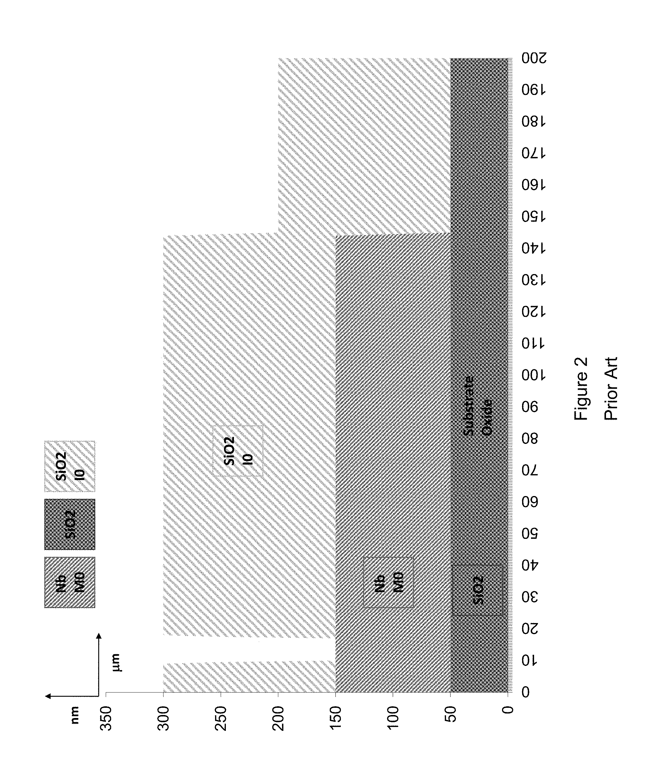
FIG. 2 shows the Second layer of the Prior Art Hypres Inc. process I0, Ion Beam deposited, dark field mask lithography defining Vias between M1 and M0, etched in CH.sub.4+O.sub.2 mixture, chemically stripped;
FIG. 3 shows the Third layer of the Prior Art Hypres Inc. process Tri-layer in situ sputter deposited Nb/Al/AlOx/Nb, I1C clear field mask lithography defining junctions hard baked photoresist, Anodization, chemically stripped;
FIG. 4 shows the Fourth layer of the Prior Art Hypres Inc. process A1, Anodization ring definition, A1 clear field mask lithography defining Josephson Junctions, Ion Beam milled, chemically stripped;
FIG. 5 shows the fifth layer of the Prior Art Hypres Inc. process M1, base electrode of the tri-layer. M1 clear field mask lithography defining inductances and interconnects by RIE, chemically stripped;
FIG. 6 shows the sixth layer of the Prior Art Hypres Inc. process R2, Sputter deposited molybdenum, clear field mask lithography defining the shunt and bias resistors of the circuit, SF.sub.6 plasma etched, chemically stripped;
FIG. 7 shows the seventh layer of the Prior Art Hypres Inc. process I1B-1 and I1B-2, PECVD deposited, I1B lithography dark field mask defining vias to Junction, resistors and contact pads, etched in CH4+O2 mixture, chemically stripped;
FIG. 8 shows the Eighth layer of the Prior Art Hypres Inc. process M2, sputter deposited niobium, clear field mask lithography defining M2 inductors and interconnects, SF.sub.6 RIE etched, chemically stripped;
FIG. 9 shows the ninth layer of the Prior Art Hypres Inc. process 12, PECVD deposited, dark field mask lithography defining vias to contact pad and M2 wiring, etched in CH4+O2 mixture, chemically stripped;
FIG. 10 shows the tenth layer of the Prior Art Hypres Inc. process M3, sputter deposited niobium, clear field mask lithography defining M3 interconnects, SF.sub.6 RIE etched, chemically stripped;
FIG. 11 shows the eleventh layer of the Prior Art Hypres Inc. process R3, Image reversal lithography using clear field mask defining R3, electron beam evaporated Ti/Pl/Au, Lift-off, chemically cleaned;
FIG. 12 show a layout of a shunted Junction of the Prior Art Hypres Inc. process, connected to bias pad with a bias resistor and grounded through the base electrode of the junction;
FIG. 13 shows the base technology level description of the RIPPLE-7 process according to the present invention, where Mn8 to M0 layers are planarized;
FIGS. 14A and 14B show the xth Superconducting metal layer extension, after plug definition;
FIGS. 15A and 15B show the Al wet etch, Pattern #2, Niobium metal RIE;
FIGS. 16A and 16B show the First Interlayer dielectric (SiO.sub.2) deposition;
FIGS. 17A and 17B show the removal of Interlayer dielectric by Reactive Ion Etch;
FIGS. 18A and 18B show the Second ILD deposition;
FIGS. 19A and 19B show the ILD Planarization by RIE SiO.sub.2 etch;
FIGS. 20A and 20B show Chemical Mechanical Planarization;
FIGS. 21A and 21B show an alternative method (using Anodization);
FIG. 22 shows a prior art 4-layer metal process;
FIG. 23 shows a planarized 6 metal layer process;
FIG. 24 shows RIPPLE-8, a process with 12 superconducting layers, Shielded passive transmission lines, shielded DC power distributions;
FIGS. 25A and 25B show schematic planarized layers according to the Prior Art; and
FIGS. 26A, 26B and 26C show via plugs and underground superconducting wire defined without aluminum etch stop; 26A After the definition of the via-plug; 26B After the deposition of the metal layer; and 26C After the definition of the wiring layer.
DETAILED DESCRIPTION OF THE PREFERRED EMBODIMENTS
1.0 Prior Art Fabrication Process
The details of a known Hypres Inc. (Elmsford N.Y.) the process flow will be described by following the cross-section of a biased, shunted Josephson junction as it made layer-by-layer. The layout of this is given in FIG. 12, which shows a layout of a shunted Junction connected to a bias pad with a bias resistor and grounded through the base electrode of the junction.
The process starts with a bare 150 mm diameter oxidized silicon wafer by deposition the first Nb metal layer (M0). Of course, other substrates may be used. Typically, the substrate is planarized before the first step, and indeed, may be a planarized circuit formed from preceding manufacturing steps.
The deposition is done in a cryo-pumped chamber to a pressure of about 10.sup.-7 Torr. Magnetron sputtering is used for deposition, where the wafer is scanned under the target at constant speed. Both the scan speed and the chamber pressure are adjusted to get the required film thickness growing without stress. At 3 kW power the wafer is scanned at 20 cm/sec to make a film of thickness 1000 .ANG. for M0 at a stress-free chamber pressure of 17 mTorr. After deposition the Nb thin film is patterned using the M0-mask, a dark field mask and a positive photoresist AZ5214-E IR. The pattern is transferred to the thin film after etching it in end-point-detected SF.sub.6 plasma RIE. Following etching, the resist and etch by-products are stripped and cleared by wet processing. The final cross section after the completion of the first layer is given in FIG. 1 (The figure is to scale with nano-meter scale on the Y-axis and micro-meter scale on the X-axis), shows a First layer--M0, sputter deposited, dark field mask lithography, SF.sub.6 RIE etched, chemically stripped. Moats and ground pad holes are defined.
The following describes the 11 layers of the standard Hypres Inc. (Elmsford N.Y.) legacy (non-planarized) fabrication process, according to a preferred embodiment:
1.1 M0--the First Niobium Superconductor Layer.
The first Niobium superconductor layer is grown to a thickness of 1000 .ANG..+-.10% and the film's sheet resistance at room temperature is 1.90.+-.0.2.OMEGA./.quadrature.. In a circuit this layer is used as grounding and most of the return current flows through it. To reduce the effect of ground current induced magnetic field interference to the operation of the circuit, a number of holes and moats are included in this layer. Holes and moats can have a minimum size of 2.times.2 .mu.m and a bias (0.25.+-.0.25) .mu.m and a minimum spacing of 3 .mu.m between them.
1.2 I0--Interlayer Dielectric Between M0 and M1.
FIG. 2 shows the Second layer I0--Ion Beam deposited, dark field mask lithography defining Vias between M1 and M0, etched in CH.sub.4+O.sub.2 mixture, chemically stripped.
The interlayer dielectric between M0 and M1 is PECVD deposited SiO.sub.2 insulator of thickness 1500 .ANG..+-.10% with a specific capacitance of 0.277 fF/.mu.m.sup.2.+-.20%. Contact to M0 is through I0 vias with a minimum size of 2.times.2 .mu.m and a bias (0.30.+-.0.25) .mu.m. The alignment tolerance of I0 to M0 is .+-.0.25 .mu.m.
1.3 I1C--Niobium Superconductor Counter Electrode of the Tri-Layer.
FIG. 3 shows the Third layer--Tri-layer in situ sputter deposited Nb/Al/AlO.sub.x/Nb, I1C clear field mask lithography defining junctions hard baked photoresist, Anodization, chemically stripped.
The Niobium superconductor counter electrode of the tri-layer is deposited by magnetron sputtering in a load locked, cryo-pumped chamber with a base pressure of 1.times.10.sup.-9 T. It is grown to a thickness of 500 .ANG..+-.10%. Junctions are defined in this layer by using a Clearfield mask I1C. The alignment tolerance of I1C to M0 and/or I0 is .+-.0.25 .mu.m. After the counter electrode is etched in SF.sub.6 plasma, the wafer is anodized.
1.4 A1--Al.sub.2O.sub.3/Nb.sub.2O.sub.5 Double Layer
FIG. 4 shows the Fourth layer--Al, Anodization ring definition, Al clear field mask lithography defining Josephson Junctions, Ion Beam milled, chemically stripped.
The A1--Al.sub.2O.sub.3/Nb.sub.2O.sub.5 double layer is grown by anodization after RIE of the base electrode by applying a constant voltage of about 28 mV and 700 mA initial current forming a double protecting layer of Al.sub.2O.sub.3 and Nb.sub.2O.sub.5. The thickness of the bi-layer is about 560 .ANG..+-.10%. After A1 definition the remaining bi-layer surrounds the Josephson junctions by about 0.5 .mu.m. A1 is aligned to I1C with an alignment tolerance of .+-.0.25 .mu.m.
1.5 M1--Niobium Superconductor Counter Electrode of the Tri-Layer.
FIG. 5 shows the fifth layer--M1, base electrode of the tri-layer. M1 clear field mask lithography defining inductances and interconnects by RIE, chemically stripped.
The Niobium superconductor counter electrode of the tri-layer is deposited by magnetron sputtering in a load locked, cryo-pumped chamber with a base pressure of 1.times.10.sup.-9 T. It is grown to a thickness of 1500 .ANG..+-.10% and the film's sheet resistance at room temperature is 1.70.+-.0.2.OMEGA./.quadrature.. Most circuit inductances are defined in this layer by micro-strip lines with M0 as ground plane and M2 for double ground plane. A specific inductance of 0.487.+-.0.007 pH with a fringing factor of 0.54.+-.0.13 .mu.m. Minimum line width 2 .mu.m and a bias (-0.30.+-.0.25) .mu.m. The alignment tolerance of M1 to M0 and/or I0 is .+-.0.25 .mu.m.
1.6 R2--Molybdenum Resistor Material.
FIG. 6 shows the sixth layer R2, Sputter deposited molybdenum, clear field mask lithography defining the shunt and bias resistors of the circuit, SF.sub.6 plasma etched, chemically stripped.
The Molybdenum resistor material is deposited by magnetron sputtering in a load locked; cryo-pumped chamber with a base pressure of 1.times.10.sup.-7 T right after the first part of the I1B1 dielectric is deposited. It is grown to a thickness of 750 .ANG..+-.10% and the film's sheet resistance at room temperature is 1.95.+-.0.1.OMEGA./.quadrature. and is reduced to 1.0.+-.0.1.OMEGA./.quadrature. at 4.2 K. Minimum line width allowed is 2 .mu.m and a bias (-0.2.+-.0.25) .mu.m. This bias is corrected on the mask. Shunt and bias resistors are defined in this layer. The alignment tolerance of R2 to I1A is .+-.0.25 .mu.m.
1.7 I1B--Interlayer Dielectric Between Tri-Layer and R2-I1B1; Tri-Layer and M2-I1B2.
FIG. 7 shows the seventh layer I1B-1 and I1B-2--PECVD deposited, I1B lithography dark field mask defining vias to Junction, resistors and contact pads, etched in CH.sub.4+O.sub.2 mixture, chemically stripped.
I1B1 and I1B2 are PECVD deposited SiO.sub.2 insulator of thickness 2000 .ANG..+-.20% with a specific capacitance of 0.416 fF/.mu.m.sup.2.+-.20%. Contact to M1 and I1A is through I1B vias with a minimum size of 2 .mu.m and a bias (0.20.+-.0.25).mu.m. The alignment tolerance of I1B to I1A is .+-.0.1 .mu.m.
1.8 M2--Niobium Superconductor Material.
FIG. 8 shows the Eighth layer--M2, sputter deposited niobium, clear field mask lithography defining M2 inductors and interconnects, SF.sub.6 RIE etched, chemically stripped.
The Niobium superconductor material is deposited by magnetron sputtering in a load locked, cryo-pumped chamber with a base pressure of 1.times.10.sup.-7 T. It is grown to a thickness of 3000 .ANG..+-.10% and the film's sheet resistance at room temperature is 1.60 .OMEGA./.quadrature..+-.10%. Minimum line width 2 .mu.m and a minimum gap between lines of 2.5 .mu.m and a bias of (-0.5.+-.0.25) .mu.m. The alignment tolerance of M2 to I1B is .+-.0.25 .mu.m. This layer is mainly used for wiring, as an inductor with M0 as a ground plane and M3 for double ground plane. A specific inductance of 0.67.+-.0.01 pH/.quadrature. and Josephson penetration and a fringing factor of 0.98.+-.0.19 .mu.m.
1.9 I2--Interlayer Dielectric Between M2 and M3.
FIG. 9 shows the ninth layer I2--PECVD deposited, dark field mask lithography defining vias to contact pad and M2 wiring, etched in CH.sub.4+O.sub.2 mixture, chemically stripped.
The interlayer dielectric between M2 and M3 is PECVD deposited SiO.sub.2 insulator of thickness 5000 .ANG..+-.10% with a specific capacitance of 0.08 fF/.mu.m.sup.2.+-.20%. Contact to M2 is through I2 vias with a minimum size of 2.times.2 .mu.m and a bias (0.20.+-.0.25) .mu.m. The alignment tolerance of I2 to M2 is .+-.0.25 .mu.m.
1.10 M3--Niobium Superconductor Material.
FIG. 10 shows the tenth layer--M3, sputter deposited niobium, clear field mask lithography defining M3 interconnects, SF.sub.6 RIE etched, chemically stripped.
The Niobium superconductor material layer is deposited by magnetron sputtering in a load locked, cryo-pumped chamber with a base pressure of 1.times.10.sup.-7 T. It is grown to a thickness of 6000 .ANG..+-.10% and the film's sheet resistance at room temperature is 0.60 .OMEGA./.quadrature..+-.10%. Minimum line width 2 .mu.m and a minimum gap between lines of 2.5 .mu.m and a bias of (-0.75.+-.0.25) .mu.m. The alignment tolerance of M3 to 12 is .+-.0.5 .mu.m. This layer is mainly used for wiring and as an inductor with M0 as a ground plane. A specific inductance of 1.26.+-.0.02 pH/.quadrature. and a fringing factor of 1.9.+-.0.1 .mu.m.
1.11 R3--Titanium/Palladium/Gold (Ti/Pl/Au) Resistor Material.
FIG. 11 shows the eleventh layer--R3, Image reversal lithography using clear field mask defining R3, electron beam evaporated Ti/Pl/Au, Lift-off, chemically cleaned.
The Titanium/Palladium/Gold (Ti/Pl/Au) resistor material is deposited by electron beam evaporation in a cryo-pumped chamber with a base pressure of 1.times.10.sup.-7 T. It is grown to a thickness of (300/1000/2000 .ANG.).+-.10% and the film's sheet resistance at room temperature is 0.23.+-.0.05.OMEGA./.quadrature. and is reduce to 0.15.+-.0.05.OMEGA./.quadrature. at 4.2 K. Minimum line width 2 .mu.m. Contact pads are defined in this layer. The alignment tolerance of R3 to M3 is .+-.0.5 .mu.m.
2 Rapid Planarized Process for Layer Extension (RIPPLE)
The RIPPLE process described below represents one embodiment of the new process for extending prior superconducting fabrication processes.
The Acronym RIPPLE stands for:
Rapid: One deposition and CMP less (.about.20% less time per layer)
Integrated: to the current standard process, by adding new wiring layers under the ground plane of the old 4-layer Process
Planarization
Process: Modified "Caldera" process (K. Hinode, et al., Physica C 412-414 (2004) 1437-1441)
Layer
Extension: Easily extendible 4+n, (n=2 has been successfully demonstrated)
All the new superconducting metal layers labeled Mn1, Mn2, Mn3 . . . are placed below the ground plane of the current process--M0. The interconnect between the layers is done through Plugs labeled In1, In2, In3 . . . . The Mnx/Inx duo is deposited at one go with a thin layer of Aluminum separating them. Although Aluminum is not superconducting at 4.2 K, the sub-nanometer thickness renders it superconducting because of the proximity effect. Once the thin film deposition of the now three layers (Mnx-Al-Inx) is done and the both the Plug and superconducting metal layer are defined through a fabrication process that involves: photolithography and reactive ion etch of the Plug; wet chemical or ion beam milling of the Aluminum; photolithography and reactive ion etch of the superconducting metal layer. The respective interlayer dielectric are deposited and partially planarized by photolithography followed by reactive ion etch. By design the photolithography is done in such a way that it leaves a rim of dielectric (20 nm wide) on the perimeter of the superconducting metal and its plug. This insures a uniform dielectric roughness throughout enabling the next process to be pattern independent. The chemical mechanical polishing is thus pattern independent and hence very uniform across the entire wafer. The technology level based on the integration level is now as follows:
1) RIPPLE-0 A process where the M0 ground plane of the legacy process is planarized with 4 superconducting layers.
2) RIPPLE-1 A process where Mn1 to M0 layers are planarized with 5 superconducting metal layers.
3) RIPPLE-2 A process where Mn2 to M0 layers are planarized with 6 superconducting metal layers.
4) RIPPLE-4 A process where Mn4 to M0 layers are planarized with 8 superconducting metal layers.
5) RIPPLE-6 A process where Mn6 to M0 layers are planarized with 10 superconducting metal layers.
6) RIPPLE-8 A process where Mn8 to M0 layers are planarized with 12 superconducting metal layers
A RIPPLE-7 process where Mn8 to M0 layers are planarized is illustrated in FIG. 13, which shows the base technology level description.
2.1 Advantages of Ripple
1) Rapid: It is estimated that it is 20% faster than a process that would could accomplish similar results by processing one layer at a time, for example CALDERA process. See, Fourie, Coenrad; Xizhu Peng; Takahashi, Akitomo; Yoshikawa, Nobuyuki, "Modeling and calibration of ADP process for inductance calculation with InductEx," Superconductive Electronics Conference (ISEC), 2013 IEEE 14th International, vol., no., pp. 1, 3, 7-11 Jul. 2013, doi: 10.1109/ISEC.2013.6604270, expressly incorporated herein by reference. This is because the superconducting wiring layer and the plug that connects it to the subsequent layer are processed in parallel.
2) Easily to implement and increase the integration level of superconducting electronic circuits. All the new layers are "underground layers" with no effect to the layers on the top. They are underground because they go under the M0 layer of the legacy process which is mainly used for grounding.
3) The Chemical Mechanical polishing part of the process has been optimized and made easy to implement by rendering it pattern independent.
4) Easily extendible, Since they same basic process is used to define all the underground layers, as a result it is easy to accommodate designs that require more layers.
5) It can be adopted to define self-aligned Josephson junctions
2.2 Ripple Process Details:
2.2.1 Mnx/Inx--Superconducting Metal Layer and Plugs Deposition (Nb--Al--Nb)
This is the first step in increasing the integration level of superconducting electronics circuits. The Niobium-Aluminum-Niobium trilayer is deposited by magnetron sputtering in a load locked, cryo-pumped chamber with a base pressure of 1.times.10.sup.-7 T. The Niobium metal layer are grown to a thickness of 2000 .ANG..+-.10% each with a 100 .ANG..+-.10% Aluminum in between. The film's sheet resistance at room temperature is 0.54.OMEGA./.quadrature..+-.10%. Minimum line width 0.8 .mu.m and a minimum gap between lines of 0.5 .mu.m and a bias of (-0.20.+-.0.20) .mu.m. This layer can be used for wiring interconnects, passive transmission lines and inductors.
2.2.1.1 Pattern Inx ("Plugs"), Reactive Ion Etch (Al as an Etch-Stop)
FIGS. 14A and 14B show the x.sup.th superconducting metal layer extension, after the plug definition.
After deposition of the tri-layer, the first step is to pattern the Plug as illustrated in FIG. 14A, which is a 3D aerial view showing two of the defined Plugs, while FIG. 14B is a cross-sectional view zooming into one of the plugs. Etching of metal and dielectric is done in two Reactive Ion Etching (RIE) systems. The first one is an RIE system with fluorine based chemistries (SF.sub.6, CHF.sub.3, CF.sub.4) and the second one is an inductively-coupled plasma (ICP) etch system equipped with both flouring and chlorine-based chemistries (Cl.sub.2, BCl.sub.3). RIE is a preferred method of etching as it is very anisotropic with high selectivity. For niobium etch the most commonly used are fluorine-based plasmas, e.g., SF.sub.6 plasma. The typical etch parameter are an SF.sub.6 gas flowing at 20 sccm in a chamber pressurized to 2 Pascal and plasma sustained with an RF power of 45.
2.2.1.2 Al Removal (Wet Etch or Anodization/Mill)
The next step is to remove the aluminum etch stop either by means of wet etch, anodization or milling.
2.2.2 Pattern #2--Mnx, Reactive Ion Etch
FIGS. 15A and 15B show the Al wet etch, Pattern #2, Niobium metal RIE.
Then photolithography is done to define the Mnx superconducting metal layer, as illustrated in FIG. 15A, shows a 3D aerial view showing two of the defined Mnx metals with their respective plugs while FIG. 15B shows a cross-sectional view. The reactive ion etch is done the same manner as the plug.
2.2.3 First Interlayer Dielectric (SiO.sub.2) Deposition (PECVD)
FIGS. 16A and 16B show the First Interlayer dielectric (SiO2) deposition.
Then SiO.sub.2 interlayer dielectric is a plasma enhanced chemical vapor deposition (PECVD) layer formed having a thickness equal to Mnx of 2000 .ANG..+-.10% with a specific capacitance of 0.24 fF/.mu.m.sup.2.+-.20%. The resulting profile is illustrated in FIG. 16A.
2.2.3.1 Pattern #2 (with 0.2-um Bias) SiO.sub.2 Planarization (RIE)
FIGS. 17A and 17B show the removal of Interlayer dielectric by Reactive Ion Etch.
The respective interlayer dielectric are deposited and partially planarized by photolithography followed by reactive ion etch. By design the photolithography is done in such a way that it leaves a rim of dielectric (20 nm wide) on the perimeter of the superconducting metal and its plug. All dielectric layers are etched in a CHF.sub.3 and O.sub.2 plasma, 8 sccm of O.sub.2 and 45 sccm of CHF.sub.3 is flown into the chamber held at a pressure of 13.33 Pa. Etching is done at 150 W RF power and the temperature on the back of the wafer is kept controlled by a chiller set to about 11.degree. C. The resulting cross section is shown in FIG. 17A.
2.2.4 SiO.sub.2 Deposition (PECVD)
FIGS. 18A and 18B show the Second ILD deposition.
Then SiO.sub.2 interlayer dielectric is plasma enhance chemical vapor deposited (PECVD) thickness equal to Inx of 2000 .ANG..+-.10% with a specific capacitance of 0.24 fF/.mu.m.sup.2.+-.20%. The resulting profile is illustrated in FIG. 18A.
2.2.4.1 Pattern #1 (with 0.2-um Bias), SiO.sub.2 Planarization (RIE)
FIGS. 19A and 19B show the ILD (interlayer dielectric) Planarization by RIE SiO.sub.2 etch.
Then photolithography is done in the same manner as pattern #1, the reactive ion etch is done in the same manner as the pattern #1, resulting in features illustrated in FIG. 19A, which shows a 3D aerial view with two of the defined Mnx metals and their respective plugs while FIG. 19B shows a cross-sectional view.
2.2.5 SiO.sub.2 Planarization (CMP)
FIGS. 20A and 20B show Chemical Mechanical Polishing Planarization.
The final, but not the least step is one that takes care of the residual interlayer dielectric on the perimeter of the metals and the plugs by chemical mechanical polishing, resulting in a structure illustrated in FIGS. 21A and 21B, which show an alternative approach to Chemical Mechanical Polishing Planarization as shown in FIGS. 20A and 20B, of achieving the same planarized metal with a plug, but the only difference being the aluminum layer that is used as an etch stop is not removed instead is anodized and kept as part of the interlayer dielectric.
FIG. 22 shows a prior art 4-layer metal process, which is not planarized, and thus has a varying topography between each layer.
FIG. 23 shows a planarized 6 metal layer process, in which lower interconnection layers have planarized topography, while the upper layers above the ground plane (magnetic shielding layer between interconnect layers and Josephson junction trilayer) are non-planar.
FIG. 24 shows a RIPPLE-8 process integrated circuit device having 12 superconducting layers (8 planarized and 4 non-planarized), shielded passive transmission lines, and shielded DC power distributions below the ground plane, and 4-layer traditional non-planarized active superconducting circuitry above the ground plane.
FIG. 25A shows a simplified picture of a completed planarized conducting layer and insulating overlayer, with the patterned wiring and via labeled. A planarized intermediate structure according to the prior art is shown in FIG. 25B. According to the prior art, two planarization steps (produced by, e.g., CMP) are therefore required to produce FIG. 25A. In contrast, in the RIPPLE process as described, the intermediate structure of FIG. 25B is never present, but a final structure that is functionally equivalent to FIG. 25A is obtained using only a single planarization step (produced by CMP). This corresponds to a fabrication process that is faster and more reliable.
3. Alternative Embodiment of RIPPLE Process
The RIPPLE process above starts with deposition of a Nb/Al/Nb trilayer, where the Al act as an etch stop. This, of course, requires later steps for the removal of this etch stop layer. An alternative embodiment of the process is also presented in FIGS. 26A, 26B, and 26C, without the need for such an etch stop or associated Al removal. The process starts with the deposition of a single 200 nm niobium thin film followed by via plugs patterning and definition (FIG. 26A). The next step is to deposit a second 200-nm thick niobium film by sputtering (FIG. 26B). During this step, the via-plugs will get coated conformally and grow together with the wiring layer. At this stage, the wiring layer is patterned and defined; the resulting structure is shown in FIG. 26C. Then 200 nm silicon dioxide (the same thickness as the wiring layer) is deposited, yielding the same structure as shown in FIGS. 16A and 16B, except for the aluminum. The rest of the process follows the RIPPLE steps described with respect to FIGS. 17-20. In this case also, only a single CMP step is needed for each wiring layer, including the via plug. This alternative embodiment may provide improved reliability and speed by skipping the aluminum etch step.
These are representative examples of the RIPPLE process, and others are also possible. The key is to pattern the vias before the wiring, which requires only a single CMP step for each wiring bi-layer in a process that can be extended to an arbitrary number of such bi-layers with small stacked vias between them.
The above description of illustrated embodiments is not intended to be exhaustive or to limit the embodiments to the precise forms disclosed. Although specific embodiments and examples are described herein for illustrative purposes, various equivalent modifications can be made without departing from the spirit and scope of the disclosure, as will be recognized by those skilled in the relevant art. The teachings provided herein of the various embodiments can be applied to other electronic systems, methods and apparatus, not necessarily the exemplary electronic systems, methods and apparatus generally described above.
As will be apparent to those skilled in the art, the various embodiments described above can be combined to provide further embodiments. Aspects of the present systems, methods and apparatus can be modified, if necessary, to employ systems, methods, apparatus and concepts of the various patents, applications and publications to provide yet further embodiments of the invention. For example, the various systems, methods and apparatus may include a different number of metal or dielectric layers than set out in the illustrated embodiments, such as three or more metal layers and two or more insulating dielectric layers alternating with the metal layers, the layers may be disposed in a different order or area, or the embodiments may omit some elements, and/or employ additional elements.
All of the U.S. patents, U.S. patent application publications, U.S. patent applications, referred to in this specification are incorporated herein by reference, in their entirety and for all purposes. Aspects of the embodiments can be modified, if necessary, to employ systems, circuits and concepts of the various patents, applications and publications to provide yet further embodiments.
These and other changes can be made to the present systems, methods and apparatus in light of the above description. In general, in the following claims, the terms used should not be construed to limit the invention to the specific embodiments disclosed in the specification and the claims, but should be construed to include all possible embodiments along with the full scope of equivalents to which such claims are entitled. Accordingly, the invention is not limited by the disclosure, but instead its scope is to be determined entirely by the following claims.
* * * * *
D00000
D00001
D00002
D00003
D00004
D00005
D00006
D00007
D00008
D00009
D00010
D00011
D00012

D00013

D00014

D00015

D00016

D00017

D00018

D00019

D00020

D00021

D00022

D00023

D00024

D00025

D00026

P00001

XML
uspto.report is an independent third-party trademark research tool that is not affiliated, endorsed, or sponsored by the United States Patent and Trademark Office (USPTO) or any other governmental organization. The information provided by uspto.report is based on publicly available data at the time of writing and is intended for informational purposes only.
While we strive to provide accurate and up-to-date information, we do not guarantee the accuracy, completeness, reliability, or suitability of the information displayed on this site. The use of this site is at your own risk. Any reliance you place on such information is therefore strictly at your own risk.
All official trademark data, including owner information, should be verified by visiting the official USPTO website at www.uspto.gov. This site is not intended to replace professional legal advice and should not be used as a substitute for consulting with a legal professional who is knowledgeable about trademark law.