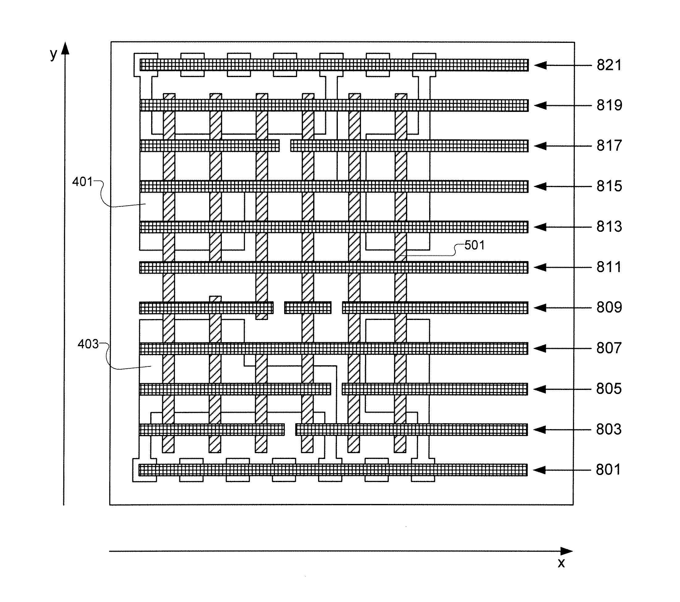
Semiconductor chip having region including gate electrode features formed in part from rectangular layout shapes on gate horizontal grid and first-metal structures formed in part from rectangular layout shapes on at least eight first-metal gridlines of first-metal vertical grid
Becker , et al. Ja
U.S. patent number 10,186,523 [Application Number 16/119,794] was granted by the patent office on 2019-01-22 for semiconductor chip having region including gate electrode features formed in part from rectangular layout shapes on gate horizontal grid and first-metal structures formed in part from rectangular layout shapes on at least eight first-metal gridlines of first-metal vertical grid. This patent grant is currently assigned to Tela Innovations, Inc.. The grantee listed for this patent is Tela Innovations, Inc.. Invention is credited to Scott T. Becker, Michael C. Smayling.


View All Diagrams
| United States Patent | 10,186,523 |
| Becker , et al. | January 22, 2019 |
Semiconductor chip having region including gate electrode features formed in part from rectangular layout shapes on gate horizontal grid and first-metal structures formed in part from rectangular layout shapes on at least eight first-metal gridlines of first-metal vertical grid
Abstract
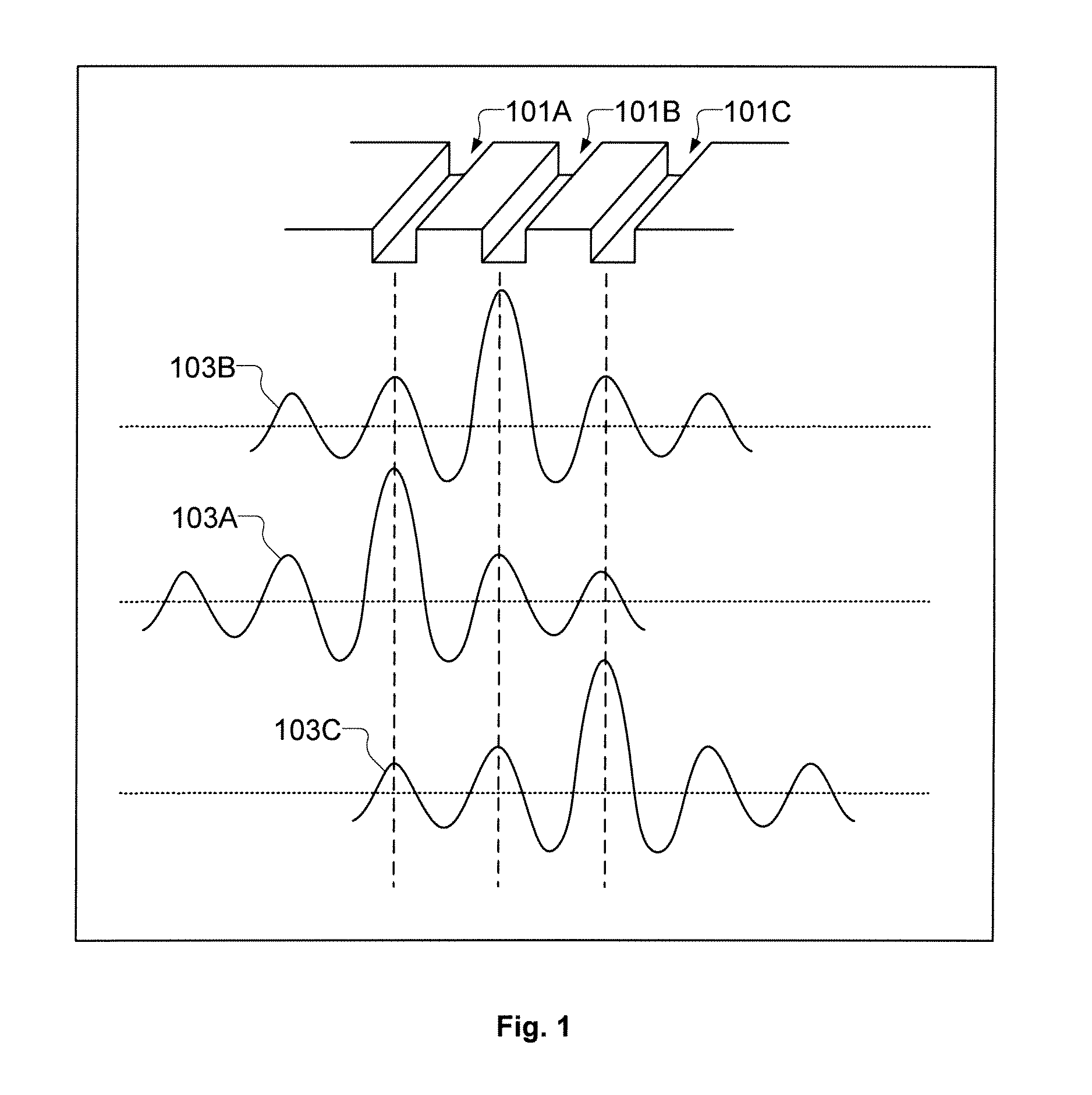
An integrated circuit includes a first gate electrode track and a second gate electrode track. The first gate electrode track includes a first gate electrode feature that forms an n-channel transistor as it crosses an n-diffusion region. The first gate electrode track does not cross a p-diffusion region. The second gate electrode track includes a second gate electrode feature that forms a p-channel transistor as it crosses a p-diffusion region. The second gate electrode track does not cross an n-diffusion region. The integrated circuit also includes a linear shaped conductor that crosses both the first and second gate electrode features in a reference direction perpendicular to the first and second gate electrode tracks. The linear shaped conductor provides electrical connection between the first and second gate electrode features.
| Inventors: | Becker; Scott T. (Scotts Valley, CA), Smayling; Michael C. (Fremont, CA) | ||||||||||
|---|---|---|---|---|---|---|---|---|---|---|---|
| Applicant: |
|
||||||||||
| Assignee: | Tela Innovations, Inc. (Los
Gatos, CA) |
||||||||||
| Family ID: | 38475620 | ||||||||||
| Appl. No.: | 16/119,794 | ||||||||||
| Filed: | August 31, 2018 |
Prior Publication Data
| Document Identifier | Publication Date | |
|---|---|---|
| US 20180374873 A1 | Dec 27, 2018 | |
Related U.S. Patent Documents
| Application Number | Filing Date | Patent Number | Issue Date | ||
|---|---|---|---|---|---|
| 13774940 | Feb 22, 2013 | ||||
| 12572225 | May 7, 2013 | 8436400 | |||
| 12212562 | Nov 30, 2010 | 7842975 | |||
| 11683402 | Nov 4, 2008 | 7446352 | |||
| 60781288 | Mar 9, 2006 | ||||
| Current U.S. Class: | 1/1 |
| Current CPC Class: | H01L 27/088 (20130101); H01L 23/5283 (20130101); H01L 27/092 (20130101); H01L 21/28123 (20130101); H01L 29/42376 (20130101); H01L 21/823871 (20130101); H01L 23/5226 (20130101); H01L 27/11807 (20130101); G06F 30/392 (20200101); G06F 30/39 (20200101); H01L 27/0207 (20130101); H01L 29/42372 (20130101); H01L 2027/11861 (20130101); H01L 2027/11864 (20130101); H01L 2027/11862 (20130101); H01L 2027/11875 (20130101); H01L 2924/0002 (20130101); H01L 2027/11888 (20130101); H01L 2027/11814 (20130101); H01L 2027/11866 (20130101); H01L 2027/11812 (20130101); H01L 2027/11855 (20130101); H01L 2027/11887 (20130101); H01L 2924/0002 (20130101); H01L 2924/00 (20130101) |
| Current International Class: | H01L 27/10 (20060101); H01L 27/092 (20060101); H01L 21/28 (20060101); H01L 29/423 (20060101); H01L 21/8238 (20060101); H01L 27/088 (20060101); G06F 17/50 (20060101); H01L 27/118 (20060101); H01L 27/02 (20060101); H01L 23/522 (20060101); H01L 23/528 (20060101) |
References Cited [Referenced By]
U.S. Patent Documents
| 3521242 | July 1970 | Katz |
| 4069493 | January 1978 | Bobenrieth |
| 4197555 | April 1980 | Uehara et al. |
| 4417161 | November 1983 | Uya |
| 4424460 | January 1984 | Best |
| 4575648 | March 1986 | Lee |
| 4602270 | July 1986 | Finegold |
| 4613940 | September 1986 | Shenton et al. |
| 4657628 | April 1987 | Holloway et al. |
| 4682202 | July 1987 | Tanizawa |
| 4745084 | May 1988 | Rowson et al. |
| 4780753 | October 1988 | Shinichi et al. |
| 4801986 | January 1989 | Chang et al. |
| 4804636 | February 1989 | Groover, III |
| 4812688 | March 1989 | Chu et al. |
| 4884115 | November 1989 | Michel et al. |
| 4890148 | December 1989 | Ikeda |
| 4928160 | May 1990 | Crafts |
| 4975756 | December 1990 | Haken et al. |
| 5005068 | April 1991 | Ikeda |
| 5047979 | September 1991 | Leung |
| 5057895 | October 1991 | Beasom |
| 5068603 | November 1991 | Mahoney |
| 5079614 | January 1992 | Khatakhotan |
| 5097422 | March 1992 | Corbin et al. |
| 5117277 | May 1992 | Yuyama et al. |
| 5121186 | June 1992 | Wong et al. |
| 5208765 | May 1993 | Turnbull |
| 5224057 | June 1993 | Igarashi |
| 5242770 | September 1993 | Chen et al. |
| 5268319 | December 1993 | Harari |
| 5298774 | March 1994 | Ueda et al. |
| 5313426 | May 1994 | Sakuma et al. |
| 5338963 | August 1994 | Klaasen |
| 5351197 | September 1994 | Upton et al. |
| 5359226 | October 1994 | DeJong |
| 5365454 | November 1994 | Nakagawa et al. |
| 5367187 | November 1994 | Yuen |
| 5378649 | January 1995 | Huang |
| 5396128 | March 1995 | Dunning et al. |
| 5420447 | May 1995 | Waggoner |
| 5461577 | October 1995 | Shaw et al. |
| 5471403 | November 1995 | Fujimaga |
| 5486717 | January 1996 | Kokubo |
| 5497334 | March 1996 | Russell et al. |
| 5497337 | March 1996 | Ponnapalli et al. |
| 5526307 | June 1996 | Lin et al. |
| 5536955 | July 1996 | Ali |
| 5545904 | August 1996 | Orbach |
| 5581098 | December 1996 | Chang |
| 5581202 | December 1996 | Yano et al. |
| 5612893 | March 1997 | Hao et al. |
| 5636002 | June 1997 | Garofalo |
| 5656861 | August 1997 | Godinho et al. |
| 5682323 | October 1997 | Pasch et al. |
| 5684311 | November 1997 | Shaw |
| 5684733 | November 1997 | Wu et al. |
| 5698873 | December 1997 | Colwell et al. |
| 5705301 | January 1998 | Garza et al. |
| 5717635 | February 1998 | Akatsu |
| 5723883 | March 1998 | Gheewalla |
| 5723908 | March 1998 | Fuchida et al. |
| 5740068 | April 1998 | Liebmann et al. |
| 5745374 | April 1998 | Matsumoto |
| 5754826 | May 1998 | Gamal |
| 5756385 | May 1998 | Yuan |
| 5764533 | June 1998 | deDood |
| 5774367 | June 1998 | Reyes et al. |
| 5780909 | July 1998 | Hayashi |
| 5789776 | August 1998 | Lancaster et al. |
| 5790417 | August 1998 | Chao et al. |
| 5796128 | August 1998 | Tran et al. |
| 5796624 | August 1998 | Sridhar et al. |
| 5798298 | August 1998 | Yang et al. |
| 5814844 | September 1998 | Nagata et al. |
| 5825203 | October 1998 | Kusunoki et al. |
| 5834851 | November 1998 | Ikeda et al. |
| 5838594 | November 1998 | Kojima |
| 5841663 | November 1998 | Sharma et al. |
| 5847421 | December 1998 | Yamaguchi |
| 5850362 | December 1998 | Sakuma et al. |
| 5852562 | December 1998 | Shinomiya et al. |
| 5858580 | January 1999 | Wang et al. |
| 5898194 | April 1999 | Gheewala |
| 5900340 | May 1999 | Reich et al. |
| 5905287 | May 1999 | Hirata |
| 5908827 | June 1999 | Sirna |
| 5915199 | June 1999 | Hsu |
| 5917207 | June 1999 | Colwell et al. |
| 5920486 | July 1999 | Beahm et al. |
| 5923059 | July 1999 | Gheewala |
| 5923060 | July 1999 | Gheewala |
| 5929469 | July 1999 | Mimoto et al. |
| 5930163 | July 1999 | Hara et al. |
| 5935763 | August 1999 | Caterer et al. |
| 5949101 | September 1999 | Aritome |
| 5973369 | October 1999 | Hayashi |
| 5973507 | October 1999 | Yamazaki |
| 5977305 | November 1999 | Wigler et al. |
| 5977574 | November 1999 | Schmitt et al. |
| 5984510 | November 1999 | Ali |
| 5998879 | December 1999 | Iwaki et al. |
| 6009251 | December 1999 | Ho et al. |
| 6026223 | February 2000 | Scepanovic et al. |
| 6026225 | February 2000 | Iwasaki |
| 6034433 | March 2000 | Beatty |
| 6037613 | March 2000 | Mariyama |
| 6037617 | March 2000 | Kumagai |
| 6044007 | March 2000 | Capodieci |
| 6054872 | April 2000 | Fudanuki et al. |
| 6063132 | May 2000 | DeCamp et al. |
| 6077310 | June 2000 | Yamamoto et al. |
| 6080206 | June 2000 | Tadokoro et al. |
| 6084255 | July 2000 | Ueda |
| 6084437 | July 2000 | Sako |
| 6091845 | July 2000 | Pierrat et al. |
| 6099584 | August 2000 | Arnold et al. |
| 6100025 | August 2000 | Wigler et al. |
| 6114071 | September 2000 | Chen et al. |
| 6144227 | November 2000 | Sato |
| 6159839 | December 2000 | Jeng et al. |
| 6166415 | December 2000 | Sakemi et al. |
| 6166560 | December 2000 | Ogura et al. |
| 6174742 | January 2001 | Sudhindranath et al. |
| 6182272 | January 2001 | Andreev et al. |
| 6194104 | February 2001 | Hsu |
| 6194252 | February 2001 | Yamaguchi |
| 6194912 | February 2001 | Or-Bach |
| 6209123 | March 2001 | Maziasz et al. |
| 6230299 | May 2001 | McSherry et al. |
| 6232173 | May 2001 | Hsu et al. |
| 6240542 | May 2001 | Kapur |
| 6249902 | June 2001 | Igusa et al. |
| 6255600 | July 2001 | Schaper |
| 6255845 | July 2001 | Wong et al. |
| 6262487 | July 2001 | Igarashi et al. |
| 6269472 | July 2001 | Garza et al. |
| 6275973 | August 2001 | Wein |
| 6282696 | August 2001 | Garza et al. |
| 6291276 | September 2001 | Gonzalez |
| 6295224 | September 2001 | Chan |
| 6297668 | October 2001 | Schober |
| 6297674 | October 2001 | Kono et al. |
| 6303252 | October 2001 | Lin |
| 6323117 | November 2001 | Noguchi |
| 6331733 | December 2001 | Or-Bach et al. |
| 6331791 | December 2001 | Huang |
| 6335250 | January 2002 | Egi |
| 6338972 | January 2002 | Sudhindranath et al. |
| 6347062 | February 2002 | Nii et al. |
| 6356112 | March 2002 | Tran et al. |
| 6359804 | March 2002 | Kuriyama et al. |
| 6370679 | April 2002 | Chang et al. |
| 6378110 | April 2002 | Ho |
| 6380592 | April 2002 | Tooher et al. |
| 6388296 | May 2002 | Hsu |
| 6393601 | May 2002 | Tanaka et al. |
| 6399972 | June 2002 | Masuda et al. |
| 6400183 | June 2002 | Yamashita et al. |
| 6408427 | June 2002 | Cong et al. |
| 6415421 | July 2002 | Anderson et al. |
| 6416907 | July 2002 | Winder et al. |
| 6417549 | July 2002 | Oh |
| 6421820 | July 2002 | Mansfield et al. |
| 6425112 | July 2002 | Bula et al. |
| 6425117 | July 2002 | Pasch et al. |
| 6426269 | July 2002 | Haffner et al. |
| 6436805 | August 2002 | Trivedi |
| 6445049 | September 2002 | Iranmanesh |
| 6445065 | September 2002 | Gheewala et al. |
| 6467072 | October 2002 | Yang et al. |
| 6469328 | October 2002 | Yanai et al. |
| 6470489 | October 2002 | Chang et al. |
| 6476493 | November 2002 | Or-Bach et al. |
| 6477695 | November 2002 | Gandhi |
| 6480032 | November 2002 | Aksamit |
| 6480989 | November 2002 | Chan et al. |
| 6482689 | November 2002 | Trivedi |
| 6492066 | December 2002 | Capodieci et al. |
| 6496965 | December 2002 | van Ginneken et al. |
| 6504186 | January 2003 | Kanamoto et al. |
| 6505327 | January 2003 | Lin |
| 6505328 | January 2003 | van Ginneken et al. |
| 6507941 | January 2003 | Leung et al. |
| 6509952 | January 2003 | Govil et al. |
| 6514849 | February 2003 | Hui et al. |
| 6516459 | February 2003 | Sahouria |
| 6523156 | February 2003 | Cirit |
| 6525350 | February 2003 | Kinoshita et al. |
| 6536028 | March 2003 | Katsioulas et al. |
| 6543039 | April 2003 | Watanabe |
| 6553544 | April 2003 | Tanaka et al. |
| 6553559 | April 2003 | Liebmann et al. |
| 6553562 | April 2003 | Capodieci et al. |
| 6566720 | May 2003 | Aldrich |
| 6570234 | May 2003 | Gardner |
| 6571140 | May 2003 | Wewalaarachchi |
| 6571379 | May 2003 | Takayama |
| 6574786 | June 2003 | Pohlenz et al. |
| 6578190 | June 2003 | Ferguson et al. |
| 6583041 | June 2003 | Capodieci |
| 6588005 | July 2003 | Kobayashi et al. |
| 6590289 | July 2003 | Shively |
| 6591207 | July 2003 | Naya et al. |
| 6609235 | August 2003 | Ramaswamy et al. |
| 6610607 | August 2003 | Armbrust et al. |
| 6617621 | September 2003 | Gheewala et al. |
| 6620561 | September 2003 | Winder et al. |
| 6621132 | September 2003 | Onishi et al. |
| 6632741 | October 2003 | Clevenger et al. |
| 6633182 | October 2003 | Pileggi et al. |
| 6635935 | October 2003 | Makino |
| 6642744 | November 2003 | Or-Bach et al. |
| 6643831 | November 2003 | Chang et al. |
| 6650014 | November 2003 | Kariyazaki |
| 6661041 | December 2003 | Keeth |
| 6662350 | December 2003 | Fried et al. |
| 6664587 | December 2003 | Guterman et al. |
| 6673638 | January 2004 | Bendik et al. |
| 6675361 | January 2004 | Crafts |
| 6677649 | January 2004 | Minami et al. |
| 6687895 | February 2004 | Zhang |
| 6690206 | February 2004 | Rikino et al. |
| 6691297 | February 2004 | Misaka et al. |
| 6700405 | March 2004 | Hirairi |
| 6703170 | March 2004 | Pindo |
| 6709880 | March 2004 | Yamamoto et al. |
| 6714903 | March 2004 | Chu et al. |
| 6732334 | May 2004 | Nakatsuka |
| 6732338 | May 2004 | Crouse et al. |
| 6732344 | May 2004 | Sakamoto et al. |
| 6734506 | May 2004 | Oyamatsu |
| 6737199 | May 2004 | Hsieh |
| 6737318 | May 2004 | Murata et al. |
| 6737347 | May 2004 | Houston et al. |
| 6745372 | June 2004 | Cote et al. |
| 6745380 | June 2004 | Bodendorf et al. |
| 6749972 | June 2004 | Yu |
| 6750555 | June 2004 | Satomi et al. |
| 6760269 | July 2004 | Nakase et al. |
| 6765245 | July 2004 | Bansal |
| 6777138 | August 2004 | Pierrat et al. |
| 6777146 | August 2004 | Samuels |
| 6787823 | September 2004 | Shibutani |
| 6789244 | September 2004 | Dasasathyan et al. |
| 6789246 | September 2004 | Mohan et al. |
| 6792591 | September 2004 | Shi et al. |
| 6792593 | September 2004 | Takashima et al. |
| 6794677 | September 2004 | Tamaki et al. |
| 6794914 | September 2004 | Sani et al. |
| 6795332 | September 2004 | Yamaoka et al. |
| 6795358 | September 2004 | Tanaka et al. |
| 6795952 | September 2004 | Stine et al. |
| 6795953 | September 2004 | Bakarian et al. |
| 6800883 | October 2004 | Furuya et al. |
| 6806180 | October 2004 | Cho |
| 6807663 | October 2004 | Cote et al. |
| 6809399 | October 2004 | Ikeda et al. |
| 6812574 | November 2004 | Tomita et al. |
| 6818389 | November 2004 | Fritze et al. |
| 6818929 | November 2004 | Tsutsumi et al. |
| 6819136 | November 2004 | Or-Bach |
| 6820248 | November 2004 | Gan |
| 6826738 | November 2004 | Cadouri |
| 6834375 | December 2004 | Stine et al. |
| 6835991 | December 2004 | Pell, III |
| 6841880 | January 2005 | Matsumoto et al. |
| 6850854 | February 2005 | Naya et al. |
| 6854096 | February 2005 | Eaton et al. |
| 6854100 | February 2005 | Chuang et al. |
| 6867073 | March 2005 | Enquist |
| 6871338 | March 2005 | Yamauchi |
| 6872990 | March 2005 | Kang |
| 6877144 | April 2005 | Rittman et al. |
| 6879511 | April 2005 | Dufourt |
| 6881523 | April 2005 | Smith |
| 6884712 | April 2005 | Yelehanka et al. |
| 6885045 | April 2005 | Hidaka |
| 6889370 | May 2005 | Kerzman et al. |
| 6897517 | May 2005 | Houdt et al. |
| 6897536 | May 2005 | Nomura et al. |
| 6898770 | May 2005 | Boluki et al. |
| 6904582 | June 2005 | Rittman et al. |
| 6918104 | July 2005 | Pierrat et al. |
| 6920079 | July 2005 | Shibayama |
| 6921982 | July 2005 | Joshi et al. |
| 6922354 | July 2005 | Ishikura et al. |
| 6924560 | August 2005 | Wang et al. |
| 6928635 | August 2005 | Pramanik et al. |
| 6931617 | August 2005 | Sanie et al. |
| 6953956 | October 2005 | Or-Bach et al. |
| 6954918 | October 2005 | Houston |
| 6957402 | October 2005 | Templeton et al. |
| 6968527 | November 2005 | Pierrat |
| 6974978 | December 2005 | Possley |
| 6977856 | December 2005 | Tanaka et al. |
| 6978436 | December 2005 | Cote et al. |
| 6978437 | December 2005 | Rittman et al. |
| 6980211 | December 2005 | Lin et al. |
| 6992394 | January 2006 | Park |
| 6992925 | January 2006 | Peng |
| 6993741 | January 2006 | Liebmann et al. |
| 6994939 | February 2006 | Ghandehari et al. |
| 6998722 | February 2006 | Madurawe |
| 7003068 | February 2006 | Kushner et al. |
| 7009862 | March 2006 | Higeta et al. |
| 7016214 | March 2006 | Kawamata |
| 7022559 | April 2006 | Barnak et al. |
| 7028285 | April 2006 | Cote et al. |
| 7041568 | May 2006 | Goldbach et al. |
| 7052972 | May 2006 | Sandhu et al. |
| 7053424 | May 2006 | Ono |
| 7063920 | June 2006 | Baba-Ali |
| 7064068 | June 2006 | Chou et al. |
| 7065731 | June 2006 | Jacques et al. |
| 7079413 | July 2006 | Tsukamoto et al. |
| 7079989 | July 2006 | Wimer |
| 7093208 | August 2006 | Williams et al. |
| 7093228 | August 2006 | Andreev et al. |
| 7103870 | September 2006 | Misaka et al. |
| 7105871 | September 2006 | Or-Bach et al. |
| 7107551 | September 2006 | de Dood et al. |
| 7115343 | October 2006 | Gordon et al. |
| 7115920 | October 2006 | Bernstein et al. |
| 7120882 | October 2006 | Kotani et al. |
| 7124386 | October 2006 | Smith et al. |
| 7126837 | October 2006 | Banachowicz et al. |
| 7132203 | November 2006 | Pierrat |
| 7137092 | November 2006 | Maeda |
| 7141853 | November 2006 | Campbell et al. |
| 7143380 | November 2006 | Anderson et al. |
| 7149999 | December 2006 | Kahng et al. |
| 7152215 | December 2006 | Smith et al. |
| 7155685 | December 2006 | Mori et al. |
| 7155689 | December 2006 | Pierrat et al. |
| 7159197 | January 2007 | Falbo et al. |
| 7174520 | February 2007 | White et al. |
| 7175940 | February 2007 | Laidig et al. |
| 7176508 | February 2007 | Joshi et al. |
| 7177215 | February 2007 | Tanaka et al. |
| 7183611 | February 2007 | Bhattacharyya |
| 7185294 | February 2007 | Zhang |
| 7188322 | March 2007 | Cohn et al. |
| 7194712 | March 2007 | Wu |
| 7200835 | April 2007 | Zhang et al. |
| 7202517 | April 2007 | Dixit et al. |
| 7205191 | April 2007 | Kobayashi |
| 7208794 | April 2007 | Hofmann et al. |
| 7214579 | May 2007 | Widdershoven et al. |
| 7219326 | May 2007 | Reed et al. |
| 7221031 | May 2007 | Ryoo et al. |
| 7225423 | May 2007 | Bhattacharya et al. |
| 7227183 | June 2007 | Donze et al. |
| 7228510 | June 2007 | Ono |
| 7231628 | June 2007 | Pack et al. |
| 7235424 | June 2007 | Chen et al. |
| 7243316 | July 2007 | White et al. |
| 7252909 | August 2007 | Shin et al. |
| 7257017 | August 2007 | Liaw |
| 7264990 | September 2007 | Rueckes et al. |
| 7266787 | September 2007 | Hughes et al. |
| 7269803 | September 2007 | Khakzadi et al. |
| 7278118 | October 2007 | Pileggi et al. |
| 7279727 | October 2007 | Ikoma et al. |
| 7287320 | October 2007 | Wang et al. |
| 7294534 | November 2007 | Iwaki |
| 7302651 | November 2007 | Allen et al. |
| 7308669 | December 2007 | Buehler et al. |
| 7312003 | December 2007 | Cote et al. |
| 7312144 | December 2007 | Cho |
| 7315994 | January 2008 | Aller et al. |
| 7327591 | February 2008 | Sadra et al. |
| 7329938 | February 2008 | Kinoshita |
| 7329953 | February 2008 | Tu |
| 7335966 | February 2008 | Ihme et al. |
| 7337421 | February 2008 | Kamat |
| 7338896 | March 2008 | Vanhaelemeersch et al. |
| 7345909 | March 2008 | Chang et al. |
| 7346885 | March 2008 | Semmler |
| 7350183 | March 2008 | Cui et al. |
| 7353492 | April 2008 | Gupta et al. |
| 7358131 | April 2008 | Bhattacharyya |
| 7360179 | April 2008 | Smith et al. |
| 7360198 | April 2008 | Rana et al. |
| 7366997 | April 2008 | Rahmat et al. |
| 7367008 | April 2008 | White et al. |
| 7376931 | May 2008 | Kokubun |
| 7383521 | June 2008 | Smith et al. |
| 7397260 | July 2008 | Chanda et al. |
| 7400627 | July 2008 | Wu et al. |
| 7402848 | July 2008 | Chang et al. |
| 7404154 | July 2008 | Venkatraman et al. |
| 7404173 | July 2008 | Wu et al. |
| 7411252 | August 2008 | Anderson et al. |
| 7421678 | September 2008 | Barnes et al. |
| 7423298 | September 2008 | Mariyama et al. |
| 7424694 | September 2008 | Ikeda |
| 7424695 | September 2008 | Tamura et al. |
| 7424696 | September 2008 | Vogel et al. |
| 7426710 | September 2008 | Zhang et al. |
| 7432562 | October 2008 | Bhattacharyya |
| 7434185 | October 2008 | Dooling et al. |
| 7441211 | October 2008 | Gupta et al. |
| 7442630 | October 2008 | Kelberlau et al. |
| 7444609 | October 2008 | Charlebois et al. |
| 7446352 | November 2008 | Becker et al. |
| 7449371 | November 2008 | Kemerling et al. |
| 7458045 | November 2008 | Cote et al. |
| 7459792 | December 2008 | Chen |
| 7465973 | December 2008 | Chang et al. |
| 7466607 | December 2008 | Hollis et al. |
| 7469396 | December 2008 | Hayashi et al. |
| 7480880 | January 2009 | Visweswariah et al. |
| 7480891 | January 2009 | Sezginer |
| 7484197 | January 2009 | Allen et al. |
| 7485934 | February 2009 | Liaw |
| 7487475 | February 2009 | Kriplani et al. |
| 7492013 | February 2009 | Correale, Jr. |
| 7500211 | March 2009 | Komaki |
| 7502275 | March 2009 | Nii et al. |
| 7503026 | March 2009 | Ichiryu et al. |
| 7504184 | March 2009 | Hung et al. |
| 7506300 | March 2009 | Sezginer et al. |
| 7508238 | March 2009 | Yamagami |
| 7509621 | March 2009 | Melvin, III |
| 7509622 | March 2009 | Sinha et al. |
| 7512017 | March 2009 | Chang |
| 7512921 | March 2009 | Shibuya |
| 7514355 | April 2009 | Katase |
| 7514959 | April 2009 | Or-Bach et al. |
| 7523429 | April 2009 | Kroyan et al. |
| 7527900 | May 2009 | Zhou et al. |
| 7535751 | May 2009 | Huang et al. |
| 7538368 | May 2009 | Yano |
| 7543262 | June 2009 | Wang et al. |
| 7563701 | July 2009 | Chang et al. |
| 7564134 | July 2009 | Yang et al. |
| 7568174 | July 2009 | Sezginer et al. |
| 7569309 | August 2009 | Walter et al. |
| 7569310 | August 2009 | Wallace et al. |
| 7569894 | August 2009 | Suzuki |
| 7575973 | August 2009 | Mokhlesi et al. |
| 7592676 | September 2009 | Nakanishi |
| 7598541 | October 2009 | Okamoto et al. |
| 7598558 | October 2009 | Hashimoto et al. |
| 7614030 | November 2009 | Hsu |
| 7625790 | December 2009 | Yang |
| 7632610 | December 2009 | Wallace et al. |
| 7640522 | December 2009 | Gupta et al. |
| 7646651 | January 2010 | Lee et al. |
| 7647574 | January 2010 | Haruki |
| 7653884 | January 2010 | Furnish et al. |
| 7665051 | February 2010 | Ludwig et al. |
| 7700466 | April 2010 | Booth et al. |
| 7712056 | May 2010 | White et al. |
| 7739627 | June 2010 | Chew et al. |
| 7749662 | July 2010 | Matthew et al. |
| 7755110 | July 2010 | Gliese et al. |
| 7770144 | August 2010 | Dellinger |
| 7781847 | August 2010 | Yang |
| 7791109 | September 2010 | Wann et al. |
| 7802219 | September 2010 | Tomar et al. |
| 7816740 | October 2010 | Houston |
| 7825437 | November 2010 | Pillarisetty et al. |
| 7842975 | November 2010 | Becker et al. |
| 7873929 | January 2011 | Kahng et al. |
| 7882456 | February 2011 | Zach |
| 7888705 | February 2011 | Becker et al. |
| 7898040 | March 2011 | Nawaz |
| 7906801 | March 2011 | Becker et al. |
| 7908578 | March 2011 | Becker et al. |
| 7910958 | March 2011 | Becker et al. |
| 7910959 | March 2011 | Becker et al. |
| 7917877 | March 2011 | Singh et al. |
| 7917879 | March 2011 | Becker et al. |
| 7923266 | April 2011 | Thijs et al. |
| 7923337 | April 2011 | Chang et al. |
| 7923757 | April 2011 | Becker et al. |
| 7926001 | April 2011 | Pierrat |
| 7932544 | April 2011 | Becker et al. |
| 7932545 | April 2011 | Becker et al. |
| 7934184 | April 2011 | Zhang |
| 7939443 | May 2011 | Fox et al. |
| 7943966 | May 2011 | Becker et al. |
| 7943967 | May 2011 | Becker et al. |
| 7948012 | May 2011 | Becker et al. |
| 7948013 | May 2011 | Becker et al. |
| 7952119 | May 2011 | Becker et al. |
| 7956421 | June 2011 | Becker |
| 7958465 | June 2011 | Lu et al. |
| 7962867 | June 2011 | White et al. |
| 7962878 | June 2011 | Melzner |
| 7962879 | June 2011 | Tang et al. |
| 7964267 | June 2011 | Lyons et al. |
| 7971160 | June 2011 | Osawa et al. |
| 7989847 | August 2011 | Becker et al. |
| 7989848 | August 2011 | Becker et al. |
| 7992122 | August 2011 | Burstein et al. |
| 7994583 | August 2011 | Inaba |
| 8004042 | August 2011 | Yang et al. |
| 8022441 | September 2011 | Becker et al. |
| 8030689 | October 2011 | Becker et al. |
| 8035133 | October 2011 | Becker et al. |
| 8044437 | October 2011 | Venkatraman et al. |
| 8058671 | November 2011 | Becker et al. |
| 8058690 | November 2011 | Chang |
| 8072003 | December 2011 | Becker et al. |
| 8072053 | December 2011 | Li |
| 8088679 | January 2012 | Becker et al. |
| 8088680 | January 2012 | Becker et al. |
| 8088681 | January 2012 | Becker et al. |
| 8088682 | January 2012 | Becker et al. |
| 8089098 | January 2012 | Becker et al. |
| 8089099 | January 2012 | Becker et al. |
| 8089100 | January 2012 | Becker et al. |
| 8089101 | January 2012 | Becker et al. |
| 8089102 | January 2012 | Becker et al. |
| 8089103 | January 2012 | Becker et al. |
| 8089104 | January 2012 | Becker et al. |
| 8101975 | January 2012 | Becker et al. |
| 8110854 | February 2012 | Becker et al. |
| 8129750 | March 2012 | Becker et al. |
| 8129751 | March 2012 | Becker et al. |
| 8129752 | March 2012 | Becker et al. |
| 8129754 | March 2012 | Becker et al. |
| 8129755 | March 2012 | Becker et al. |
| 8129756 | March 2012 | Becker et al. |
| 8129757 | March 2012 | Becker et al. |
| 8129819 | March 2012 | Becker et al. |
| 8130529 | March 2012 | Tanaka |
| 8134183 | March 2012 | Becker et al. |
| 8134184 | March 2012 | Becker et al. |
| 8134185 | March 2012 | Becker et al. |
| 8134186 | March 2012 | Becker et al. |
| 8138525 | March 2012 | Becker et al. |
| 8161427 | April 2012 | Morgenshtein et al. |
| 8178905 | May 2012 | Toubou |
| 8178909 | May 2012 | Venkatraman et al. |
| 8198656 | June 2012 | Becker et al. |
| 8207053 | June 2012 | Becker et al. |
| 8214778 | July 2012 | Quandt et al. |
| 8217428 | July 2012 | Becker et al. |
| 8225239 | July 2012 | Reed et al. |
| 8225261 | July 2012 | Hong et al. |
| 8245180 | August 2012 | Smayling et al. |
| 8247846 | August 2012 | Becker |
| 8253172 | August 2012 | Becker et al. |
| 8253173 | August 2012 | Becker et al. |
| 8258547 | September 2012 | Becker et al. |
| 8258548 | September 2012 | Becker et al. |
| 8258549 | September 2012 | Becker et al. |
| 8258550 | September 2012 | Becker et al. |
| 8258551 | September 2012 | Becker et al. |
| 8258552 | September 2012 | Becker et al. |
| 8258581 | September 2012 | Becker et al. |
| 8264007 | September 2012 | Becker et al. |
| 8264008 | September 2012 | Becker et al. |
| 8264009 | September 2012 | Becker et al. |
| 8264044 | September 2012 | Becker |
| 8274099 | September 2012 | Becker |
| 8283701 | October 2012 | Becker et al. |
| 8294212 | October 2012 | Wang et al. |
| 8316327 | November 2012 | Herold |
| 8356268 | January 2013 | Becker et al. |
| 8363455 | January 2013 | Rennie |
| 8378407 | February 2013 | Audzeyeu et al. |
| 8395224 | March 2013 | Becker et al. |
| 8402397 | March 2013 | Robles et al. |
| 8405163 | March 2013 | Becker et al. |
| 8422274 | April 2013 | Tomita et al. |
| 8436400 | May 2013 | Becker et al. |
| 8453094 | May 2013 | Kornachuk et al. |
| 8575706 | November 2013 | Becker et al. |
| 8667443 | March 2014 | Smayling et al. |
| 8701071 | April 2014 | Kornachuk et al. |
| 8735995 | May 2014 | Becker et al. |
| 8756551 | June 2014 | Becker et al. |
| 8836045 | September 2014 | Becker et al. |
| 8839162 | September 2014 | Amundson et al. |
| 8839175 | September 2014 | Smayling et al. |
| 8847329 | September 2014 | Becker et al. |
| 8863063 | October 2014 | Becker et al. |
| 8921896 | December 2014 | Becker et al. |
| 9006841 | April 2015 | Kumar |
| 9035359 | May 2015 | Becker |
| 9202779 | December 2015 | Kornachuk et al. |
| 9269423 | February 2016 | Sever |
| 9336344 | May 2016 | Smayling |
| 9425272 | August 2016 | Becker |
| 9425273 | August 2016 | Becker |
| 9443947 | September 2016 | Becker |
| 9633987 | April 2017 | Smayling |
| 2001/0049813 | December 2001 | Chan et al. |
| 2002/0003270 | January 2002 | Makino |
| 2002/0015899 | February 2002 | Chen et al. |
| 2002/0024049 | February 2002 | Nii |
| 2002/0030510 | March 2002 | Kono et al. |
| 2002/0063582 | May 2002 | Rikino |
| 2002/0068423 | June 2002 | Park et al. |
| 2002/0079516 | June 2002 | Lim |
| 2002/0079927 | June 2002 | Katoh et al. |
| 2002/0149392 | October 2002 | Cho |
| 2002/0166107 | November 2002 | Capodieci et al. |
| 2002/0194575 | December 2002 | Allen et al. |
| 2003/0042930 | March 2003 | Pileggi et al. |
| 2003/0046653 | March 2003 | Liu |
| 2003/0061592 | March 2003 | Agrawal et al. |
| 2003/0088839 | May 2003 | Watanabe |
| 2003/0088842 | May 2003 | Cirit |
| 2003/0090924 | May 2003 | Nii |
| 2003/0103176 | June 2003 | Abe et al. |
| 2003/0106037 | June 2003 | Moniwa et al. |
| 2003/0107085 | June 2003 | Gudesen et al. |
| 2003/0117168 | June 2003 | Uneme et al. |
| 2003/0124847 | July 2003 | Houston et al. |
| 2003/0125917 | July 2003 | Rich et al. |
| 2003/0126569 | July 2003 | Rich et al. |
| 2003/0128565 | July 2003 | Tomita |
| 2003/0145288 | July 2003 | Wang et al. |
| 2003/0145299 | July 2003 | Fried et al. |
| 2003/0177465 | September 2003 | MacLean et al. |
| 2003/0185076 | October 2003 | Worley |
| 2003/0203287 | October 2003 | Miyagawa |
| 2003/0229868 | December 2003 | White et al. |
| 2003/0229875 | December 2003 | Smith et al. |
| 2004/0029372 | February 2004 | Jang et al. |
| 2004/0049754 | March 2004 | Liao et al. |
| 2004/0063038 | April 2004 | Shin et al. |
| 2004/0115539 | June 2004 | Broeke et al. |
| 2004/0139412 | July 2004 | Ito et al. |
| 2004/0145028 | July 2004 | Matsumoto et al. |
| 2004/0153979 | August 2004 | Chang |
| 2004/0161878 | August 2004 | Or-Bach et al. |
| 2004/0164360 | August 2004 | Nishida et al. |
| 2004/0169201 | September 2004 | Hidaka |
| 2004/0194050 | September 2004 | Hwang et al. |
| 2004/0196705 | October 2004 | Ishikura et al. |
| 2004/0229135 | November 2004 | Wang et al. |
| 2004/0232444 | November 2004 | Shimizu |
| 2004/0243966 | December 2004 | Dellinger |
| 2004/0245547 | December 2004 | Stipe |
| 2004/0262640 | December 2004 | Suga |
| 2005/0001271 | January 2005 | Kobayashi |
| 2005/0009312 | January 2005 | Butt et al. |
| 2005/0009344 | January 2005 | Hwang et al. |
| 2005/0012157 | January 2005 | Cho et al. |
| 2005/0044522 | February 2005 | Maeda |
| 2005/0055828 | March 2005 | Wang et al. |
| 2005/0076320 | April 2005 | Maeda |
| 2005/0087806 | April 2005 | Hokazono |
| 2005/0093147 | May 2005 | Tu |
| 2005/0101112 | May 2005 | Rueckes et al. |
| 2005/0110130 | May 2005 | Kitabayashi et al. |
| 2005/0135134 | June 2005 | Yen et al. |
| 2005/0136340 | June 2005 | Baselmans et al. |
| 2005/0138598 | June 2005 | Kokubun |
| 2005/0156200 | July 2005 | Kinoshita |
| 2005/0185325 | August 2005 | Hur |
| 2005/0189604 | September 2005 | Gupta et al. |
| 2005/0189614 | September 2005 | Ihme et al. |
| 2005/0196685 | September 2005 | Wang et al. |
| 2005/0205894 | September 2005 | Sumikawa et al. |
| 2005/0212018 | September 2005 | Schoellkopf et al. |
| 2005/0224982 | October 2005 | Kemerling et al. |
| 2005/0229130 | October 2005 | Wu et al. |
| 2005/0251771 | November 2005 | Robles |
| 2005/0264320 | December 2005 | Chan et al. |
| 2005/0264324 | December 2005 | Nakazato |
| 2005/0266621 | December 2005 | Kim |
| 2005/0268256 | December 2005 | Tsai et al. |
| 2005/0274983 | December 2005 | Hayashi et al. |
| 2005/0278673 | December 2005 | Kawachi |
| 2005/0280031 | December 2005 | Yano |
| 2006/0036976 | February 2006 | Cohn |
| 2006/0038234 | February 2006 | Liaw |
| 2006/0050588 | March 2006 | Osada |
| 2006/0063334 | March 2006 | Donze et al. |
| 2006/0065893 | March 2006 | Jin et al. |
| 2006/0070018 | March 2006 | Semmler |
| 2006/0084261 | April 2006 | Iwaki |
| 2006/0091550 | May 2006 | Shimazaki et al. |
| 2006/0095872 | May 2006 | McElvain |
| 2006/0101370 | May 2006 | Cui et al. |
| 2006/0112355 | May 2006 | Pileggi et al. |
| 2006/0113533 | June 2006 | Tamaki et al. |
| 2006/0113567 | June 2006 | Ohmori et al. |
| 2006/0120143 | June 2006 | Liaw |
| 2006/0121715 | June 2006 | Chang et al. |
| 2006/0123376 | June 2006 | Vogel et al. |
| 2006/0125024 | June 2006 | Ishigaki |
| 2006/0131609 | June 2006 | Kinoshita et al. |
| 2006/0136848 | June 2006 | Ichiryu et al. |
| 2006/0146638 | July 2006 | Chang et al. |
| 2006/0151810 | July 2006 | Ohshige |
| 2006/0158270 | July 2006 | Gibet et al. |
| 2006/0170108 | August 2006 | Hiroi |
| 2006/0177744 | August 2006 | Bodendorf et al. |
| 2006/0181310 | August 2006 | Rhee |
| 2006/0195809 | August 2006 | Cohn et al. |
| 2006/0195810 | August 2006 | Morton |
| 2006/0197557 | September 2006 | Chung |
| 2006/0203530 | September 2006 | Venkatraman et al. |
| 2006/0206854 | September 2006 | Barnes et al. |
| 2006/0223302 | October 2006 | Chang et al. |
| 2006/0248495 | November 2006 | Sezginer |
| 2006/0261417 | November 2006 | Suzuki |
| 2006/0277521 | December 2006 | Chen |
| 2006/0289861 | December 2006 | Correale, Jr. |
| 2007/0001304 | January 2007 | Liaw |
| 2007/0002617 | January 2007 | Houston |
| 2007/0004147 | January 2007 | Toubou |
| 2007/0007574 | January 2007 | Ohsawa |
| 2007/0038973 | February 2007 | Li et al. |
| 2007/0074145 | March 2007 | Tanaka |
| 2007/0094634 | April 2007 | Seizginer et al. |
| 2007/0101305 | May 2007 | Smith et al. |
| 2007/0105023 | May 2007 | Zhou et al. |
| 2007/0106971 | May 2007 | Lien et al. |
| 2007/0113216 | May 2007 | Zhang |
| 2007/0172770 | July 2007 | Witters et al. |
| 2007/0186196 | August 2007 | Tanaka |
| 2007/0196958 | August 2007 | Bhattacharya et al. |
| 2007/0204253 | August 2007 | Murakawa |
| 2007/0209029 | September 2007 | Ivonin et al. |
| 2007/0210391 | September 2007 | Becker et al. |
| 2007/0211521 | September 2007 | Kawasumi |
| 2007/0234252 | October 2007 | Visweswariah et al. |
| 2007/0234262 | October 2007 | Uedi et al. |
| 2007/0241810 | October 2007 | Onda |
| 2007/0251771 | November 2007 | Huang |
| 2007/0256039 | November 2007 | White |
| 2007/0257277 | November 2007 | Takeda et al. |
| 2007/0264758 | November 2007 | Correale |
| 2007/0274140 | November 2007 | Joshi et al. |
| 2007/0277129 | November 2007 | Allen et al. |
| 2007/0288882 | December 2007 | Kniffin et al. |
| 2007/0290361 | December 2007 | Chen |
| 2007/0294652 | December 2007 | Bowen |
| 2007/0297249 | December 2007 | Chang et al. |
| 2008/0001176 | January 2008 | Gopalakrishnan |
| 2008/0005712 | January 2008 | Charlebois et al. |
| 2008/0021689 | January 2008 | Yamashita et al. |
| 2008/0022247 | January 2008 | Kojima et al. |
| 2008/0046846 | February 2008 | Chew et al. |
| 2008/0073717 | March 2008 | Ha |
| 2008/0081472 | April 2008 | Tanaka |
| 2008/0082952 | April 2008 | O'Brien |
| 2008/0086712 | April 2008 | Fujimoto |
| 2008/0097641 | April 2008 | Miyashita et al. |
| 2008/0098334 | April 2008 | Pileggi et al. |
| 2008/0098341 | April 2008 | Kobayashi et al. |
| 2008/0099795 | May 2008 | Bernstein et al. |
| 2008/0127000 | May 2008 | Majumder et al. |
| 2008/0127029 | May 2008 | Graur et al. |
| 2008/0134128 | June 2008 | Blatchford et al. |
| 2008/0144361 | June 2008 | Wong |
| 2008/0148216 | June 2008 | Chan et al. |
| 2008/0163141 | July 2008 | Scheffer et al. |
| 2008/0168406 | July 2008 | Rahmat et al. |
| 2008/0169868 | July 2008 | Toubou |
| 2008/0211028 | September 2008 | Suzuki |
| 2008/0216207 | September 2008 | Tsai |
| 2008/0244494 | October 2008 | McCullen |
| 2008/0251779 | October 2008 | Kakoschke et al. |
| 2008/0265290 | October 2008 | Nielsen et al. |
| 2008/0276105 | November 2008 | Hoberman et al. |
| 2008/0283910 | November 2008 | Dreeskornfeld et al. |
| 2008/0283925 | November 2008 | Berthold et al. |
| 2008/0285331 | November 2008 | Torok et al. |
| 2008/0308848 | December 2008 | Inaba |
| 2008/0308880 | December 2008 | Inaba |
| 2008/0315258 | December 2008 | Masuda et al. |
| 2009/0014811 | January 2009 | Becker et al. |
| 2009/0024974 | January 2009 | Yamada |
| 2009/0031261 | January 2009 | Smith et al. |
| 2009/0032898 | February 2009 | Becker et al. |
| 2009/0032967 | February 2009 | Becker et al. |
| 2009/0037864 | February 2009 | Becker et al. |
| 2009/0057780 | March 2009 | Wong et al. |
| 2009/0075485 | March 2009 | Ban et al. |
| 2009/0077524 | March 2009 | Nagamura |
| 2009/0085067 | April 2009 | Hayashi et al. |
| 2009/0087991 | April 2009 | Yatsuda et al. |
| 2009/0101940 | April 2009 | Barrows et al. |
| 2009/0106714 | April 2009 | Culp et al. |
| 2009/0155990 | June 2009 | Yanagidaira et al. |
| 2009/0159950 | June 2009 | Ishibashi |
| 2009/0181314 | July 2009 | Shyu et al. |
| 2009/0187871 | July 2009 | Cork |
| 2009/0206443 | August 2009 | Juengling |
| 2009/0224408 | September 2009 | Fox |
| 2009/0228853 | September 2009 | Hong et al. |
| 2009/0228857 | September 2009 | Kornachuk et al. |
| 2009/0235215 | September 2009 | Lavin |
| 2009/0273100 | November 2009 | Aton et al. |
| 2009/0280582 | November 2009 | Thijs et al. |
| 2009/0283921 | November 2009 | Wang |
| 2009/0302372 | December 2009 | Chang et al. |
| 2009/0319977 | December 2009 | Saxena et al. |
| 2010/0001321 | January 2010 | Becker et al. |
| 2010/0006897 | January 2010 | Becker et al. |
| 2010/0006898 | January 2010 | Becker et al. |
| 2010/0006899 | January 2010 | Becker et al. |
| 2010/0006900 | January 2010 | Becker et al. |
| 2010/0006901 | January 2010 | Becker et al. |
| 2010/0006902 | January 2010 | Becker et al. |
| 2010/0006903 | January 2010 | Becker et al. |
| 2010/0006947 | January 2010 | Becker et al. |
| 2010/0006948 | January 2010 | Becker et al. |
| 2010/0006950 | January 2010 | Becker et al. |
| 2010/0006951 | January 2010 | Becker et al. |
| 2010/0006986 | January 2010 | Becker et al. |
| 2010/0011327 | January 2010 | Becker et al. |
| 2010/0011328 | January 2010 | Becker et al. |
| 2010/0011329 | January 2010 | Becker et al. |
| 2010/0011330 | January 2010 | Becker et al. |
| 2010/0011331 | January 2010 | Becker et al. |
| 2010/0011332 | January 2010 | Becker et al. |
| 2010/0011333 | January 2010 | Becker et al. |
| 2010/0012981 | January 2010 | Becker et al. |
| 2010/0012982 | January 2010 | Becker et al. |
| 2010/0012983 | January 2010 | Becker et al. |
| 2010/0012984 | January 2010 | Becker et al. |
| 2010/0012985 | January 2010 | Becker et al. |
| 2010/0012986 | January 2010 | Becker et al. |
| 2010/0017766 | January 2010 | Becker et al. |
| 2010/0017767 | January 2010 | Becker et al. |
| 2010/0017768 | January 2010 | Becker et al. |
| 2010/0017769 | January 2010 | Becker et al. |
| 2010/0017770 | January 2010 | Becker et al. |
| 2010/0017771 | January 2010 | Becker et al. |
| 2010/0017772 | January 2010 | Becker et al. |
| 2010/0019280 | January 2010 | Becker et al. |
| 2010/0019281 | January 2010 | Becker et al. |
| 2010/0019282 | January 2010 | Becker et al. |
| 2010/0019283 | January 2010 | Becker et al. |
| 2010/0019284 | January 2010 | Becker et al. |
| 2010/0019285 | January 2010 | Becker et al. |
| 2010/0019286 | January 2010 | Becker et al. |
| 2010/0019287 | January 2010 | Becker et al. |
| 2010/0019288 | January 2010 | Becker et al. |
| 2010/0019308 | January 2010 | Chan et al. |
| 2010/0023906 | January 2010 | Becker et al. |
| 2010/0023907 | January 2010 | Becker et al. |
| 2010/0023908 | January 2010 | Becker et al. |
| 2010/0023911 | January 2010 | Becker et al. |
| 2010/0025731 | February 2010 | Becker et al. |
| 2010/0025732 | February 2010 | Becker et al. |
| 2010/0025733 | February 2010 | Becker et al. |
| 2010/0025734 | February 2010 | Becker et al. |
| 2010/0025735 | February 2010 | Becker et al. |
| 2010/0025736 | February 2010 | Becker et al. |
| 2010/0032722 | February 2010 | Becker et al. |
| 2010/0032723 | February 2010 | Becker et al. |
| 2010/0032724 | February 2010 | Becker et al. |
| 2010/0032726 | February 2010 | Becker et al. |
| 2010/0037194 | February 2010 | Becker et al. |
| 2010/0037195 | February 2010 | Becker et al. |
| 2010/0096671 | April 2010 | Becker et al. |
| 2010/0115484 | May 2010 | Frederick |
| 2010/0187609 | July 2010 | Moroz |
| 2010/0203689 | August 2010 | Bernstein et al. |
| 2010/0224943 | September 2010 | Kawasaki |
| 2010/0229140 | September 2010 | Werner et al. |
| 2010/0232212 | September 2010 | Anderson et al. |
| 2010/0252865 | October 2010 | Van Der Zanden |
| 2010/0252896 | October 2010 | Smayling |
| 2010/0264468 | October 2010 | Xu |
| 2010/0270681 | October 2010 | Bird et al. |
| 2010/0287518 | November 2010 | Becker |
| 2010/0301482 | December 2010 | Schultz et al. |
| 2011/0014786 | January 2011 | Sezginer |
| 2011/0016909 | January 2011 | Mirza et al. |
| 2011/0108890 | May 2011 | Becker et al. |
| 2011/0108891 | May 2011 | Becker et al. |
| 2011/0154281 | June 2011 | Zach |
| 2011/0207298 | August 2011 | Anderson et al. |
| 2011/0260253 | October 2011 | Inaba |
| 2011/0298025 | December 2011 | Haensch et al. |
| 2011/0317477 | December 2011 | Liaw |
| 2012/0012932 | January 2012 | Perng et al. |
| 2012/0118854 | May 2012 | Smayling |
| 2012/0131528 | May 2012 | Chen |
| 2012/0273841 | November 2012 | Quandt et al. |
| 2013/0097574 | April 2013 | Balabanov et al. |
| 2013/0200465 | August 2013 | Becker et al. |
| 2013/0200469 | August 2013 | Becker et al. |
| 2013/0207198 | August 2013 | Becker et al. |
| 2013/0207199 | August 2013 | Becker et al. |
| 2013/0254732 | September 2013 | Kornachuk et al. |
| 2014/0197543 | July 2014 | Kornachuk et al. |
| 2015/0249041 | September 2015 | Becker et al. |
| 2015/0270218 | September 2015 | Becker et al. |
| 2016/0079159 | March 2016 | Kornachuk et al. |
| 2016/0079276 | March 2016 | Becker et al. |
| 0102644 | Jul 1989 | EP | |||
| 0788166 | Aug 1997 | EP | |||
| 1394858 | Mar 2004 | EP | |||
| 1670062 | Jun 2006 | EP | |||
| 1833091 | Aug 2007 | EP | |||
| 1730777 | Sep 2007 | EP | |||
| 2251901 | Nov 2010 | EP | |||
| 2860920 | Apr 2005 | FR | |||
| 58-182242 | Oct 1983 | JP | |||
| 58-215827 | Dec 1983 | JP | |||
| 61-182244 | Aug 1986 | JP | |||
| S61-202451 | Sep 1986 | JP | |||
| S62-047148 | Feb 1987 | JP | |||
| S63-310136 | Dec 1988 | JP | |||
| H01284115 | Nov 1989 | JP | |||
| 03-165061 | Jul 1991 | JP | |||
| H05152937 | Jun 1993 | JP | |||
| H05211437 | Aug 1993 | JP | |||
| H05218362 | Aug 1993 | JP | |||
| H07-153927 | Jun 1995 | JP | |||
| 2684980 | Jul 1995 | JP | |||
| 1995-302706 | Nov 1995 | JP | |||
| 09-282349 | Oct 1997 | JP | |||
| 1997-09289251 | Nov 1997 | JP | |||
| 10-116911 | May 1998 | JP | |||
| 1999-045948 | Feb 1999 | JP | |||
| 2000-164811 | Jun 2000 | JP | |||
| 2001-068558 | Mar 2001 | JP | |||
| 2001-168707 | Jun 2001 | JP | |||
| 2001-306641 | Nov 2001 | JP | |||
| 2002-026125 | Jan 2002 | JP | |||
| 2002-026296 | Jan 2002 | JP | |||
| 2002-184870 | Jun 2002 | JP | |||
| 2001-056463 | Sep 2002 | JP | |||
| 2002-258463 | Sep 2002 | JP | |||
| 2002-289703 | Oct 2002 | JP | |||
| 2001-272228 | Mar 2003 | JP | |||
| 2003-100872 | Apr 2003 | JP | |||
| 2003-264231 | Sep 2003 | JP | |||
| 2004-013920 | Jan 2004 | JP | |||
| 2004-200300 | Jul 2004 | JP | |||
| 2004-241529 | Aug 2004 | JP | |||
| 2004-342757 | Dec 2004 | JP | |||
| 2005-020008 | Jan 2005 | JP | |||
| 2003-359375 | May 2005 | JP | |||
| 2005-123537 | May 2005 | JP | |||
| 2005-135971 | May 2005 | JP | |||
| 2005-149265 | Jun 2005 | JP | |||
| 2005-183793 | Jul 2005 | JP | |||
| 2005-203447 | Jul 2005 | JP | |||
| 2005-268610 | Sep 2005 | JP | |||
| 2006-073696 | Mar 2006 | JP | |||
| 2005-114752 | Oct 2006 | JP | |||
| 2006-303022 | Nov 2006 | JP | |||
| 2007-012855 | Jan 2007 | JP | |||
| 2007-013060 | Jan 2007 | JP | |||
| 2007-043049 | Feb 2007 | JP | |||
| 2007-141971 | Jun 2007 | JP | |||
| 2010-141047 | Jun 2010 | JP | |||
| 2011-515841 | May 2011 | JP | |||
| 10-0417093 | Jun 1997 | KR | |||
| 10-1998-087485 | Dec 1998 | KR | |||
| 1998-0084215 | Dec 1998 | KR | |||
| 10-1999-0057943 | Jul 1999 | KR | |||
| 2000-0005660 | Jan 2000 | KR | |||
| 10-2000-0028830 | May 2000 | KR | |||
| 10-2002-0034313 | May 2002 | KR | |||
| 10-2002-0070777 | Sep 2002 | KR | |||
| 2003-0022006 | Mar 2003 | KR | |||
| 2004-0005609 | Jan 2004 | KR | |||
| 10-2005-0030347 | Mar 2005 | KR | |||
| 2005-0037965 | Apr 2005 | KR | |||
| 2006-0108233 | Oct 2006 | KR | |||
| 10-2007-0077162 | Jul 2007 | KR | |||
| 386288 | Apr 2000 | TW | |||
| 200423404 | Nov 2004 | TW | |||
| 200426632 | Dec 2004 | TW | |||
| 200534132 | Oct 2005 | TW | |||
| 200620017 | Jun 2006 | TW | |||
| 200630838 | Sep 2006 | TW | |||
| 200709309 | Mar 2007 | TW | |||
| 200709565 | Mar 2007 | TW | |||
| 200811704 | Mar 2008 | TW | |||
| 200947567 | Nov 2009 | TW | |||
| WO 2005/104356 | Nov 2005 | WO | |||
| WO 2006/014849 | Feb 2006 | WO | |||
| WO 2006/052738 | May 2006 | WO | |||
| WO 2006/090445 | Aug 2006 | WO | |||
| WO 2007/014053 | Feb 2007 | WO | |||
| WO 2007/063990 | Jun 2007 | WO | |||
| WO 2007/103587 | Sep 2007 | WO | |||
| WO 2009/054936 | Apr 2009 | WO | |||
Other References
|
US. Appl. No. 60/625,342, filed May 25, 2006, Pileggi et al. cited by applicant . Acar, et al., "A Linear-Centric Simulation Framework for Parametric Fluctuations", 2002, IEEE, Carnegie Mellon University USA, pp. 1-8. cited by applicant . Amazawa, et al., "Fully Planarized Four-Level Interconnection with Stacked VLAS Using CMP of Selective CVD-A1 and Insulator and its Application to Quarter Micron Gate Array LSIs", 1995, IEEE, Japan, pp. 473-476. cited by applicant . Axelrad et al. "Efficient Full-Chip Yield Analysis Methodology for OPC-Corrected VLSI Design", 2000, International Symposium on Quality Electronic Design (ISQED). cited by applicant . Balasinski et al. "Impact of Subwavelength CD Tolerance on Device Performance", 2002, SPIE. cited by applicant . Burkhardt, et al., "Dark Field Double Dipole Lithography (DDL) for Back-End-Of-Line Processes", 2007, SPIE Proceeding Series, vol. 6520; 65200K. cited by applicant . Capetti, et al., "Sub k1=0.25 Lithography with Double Patterning Technique for 45nm Technology Node Flash Memory Devices at .lamda.=193nm", 2007, SPIE Proceeding Series, vol. 6520; 65202K. cited by applicant . Capodieci, L., et al., "Toward a Methodology for Manufacturability-Driven Design Rule Exploration," DAC 2004, Jun. 7-11, 2004, San Diego, CA. cited by applicant . Chandra, et al., "An Interconnect Channel Design Methodology for High Performance Integrated Circuits", 2004, IEEE, Carnegie Mellon University, pp. 1-6. cited by applicant . Cheng, et al., "Feasibility Study of Splitting Pitch Technology on 45nm Contact Patterning with 0.93 NA", 2007, SPIE Proceeding Series, vol. 6520; 65202N. cited by applicant . Chow, et al., "The Design of a SRAM-Based Field-Programmable Gate Array--Part II: Circuit Design and Layout", 1999, IEEE, vol. 7 # 3 pp. 321-330. cited by applicant . Clark et al. "Managing Standby and Active Mode Leakage Power in Deep Sub-Micron Design", Aug. 9-11, 2004, ACM. cited by applicant . Cobb et al. "Using OPC to Optimize for Image Slope and Improve Process Window", 2003, SPIE. cited by applicant . Devgan "Leakage Issues in IC Design: Part 3", 2003, CCAD. cited by applicant . DeVor, et al., "Statistical Quality Design and Control", 1992, Macmillan Publishing Company, pp. 264-267. cited by applicant . Dictionary.com, "channel," in Collins English Dictionary--Complete & Unabridged 10th Edition. Source location: HarperCollins Publishers. http://dictionary.reference.com/browse/channel. Available: http://dictionary.reference.com. cited by applicant . Dusa, et al. "Pitch Doubling Through Dual Patterning Lithography Challenges in Integration and Litho Budgets", 2007, SPIE Proceeding Series, vol. 6520; 65200G. cited by applicant . El-Gamal, "Fast, Cheap and Under Control: The Next Implementation Fabric", Jun. 2-6, 2003, ACM Press, pp. 354-355. cited by applicant . Firedberg, et al., "Modeling Within-Field Gate Length Spatial Variation for Process-Design Co-Optimization," 2005 Proc. of SPIE vol. 5756, pp. 178-188. cited by applicant . Frankel, "Quantum State Control Interference Lithography and Trim Double Patterning for 32-16nm Lithography", 2007, SPIE Proceeding Series, vol. 6520; 65202L. cited by applicant . Garg, et al. " Lithography Driven Layout Design", 2005, IEEE. cited by applicant . Grobman et al. "Reticle Enhancement Technology Trends: Resource and Manufacturability Implications for the Implementation of Physical Designs" Apr. 1-4, 2001, ACM. cited by applicant . Grobman et al. "Reticle Enhancement Technology: Implications and Challenges for Physical Design" Jun. 18-22, 2001, ACM. cited by applicant . Gupta et al. " Enhanced Resist and Etch CD Control by Design Perturbation", Oct. 4-7, 2006, Society of Photo-Optical Instrumentation Engineers. cited by applicant . Gupta et al. "A Practical Transistor-Level Dual Threshold Voltage Assignment Methodology", 2005, Sixth International Symposium on Quality Electronic Design (ISQED). cited by applicant . Gupta et al. "Detailed Placement for Improved Depth of Focus and CD Control", 2005, ACM. cited by applicant . Gupta et al. "Joining the Design and Mask Flows for Better and Cheaper Masks", Oct. 14-17, 2004, Society of Photo-Optical Instrumentation Engineers. cited by applicant . Gupta et al. "Manufacturing-Aware Physical Design", 2003, ACM. cited by applicant . Gupta et al. "Selective Gate-Length Biasing for Cost-Effective Runtime Leakage Control", Jun. 7-11, 2004, ACM. cited by applicant . Gupta et al. "Wafer Topography-Aware Optical Proximity Correction for Better DOF Margin and CD Control", Apr. 13-15, 2005, SPIE. cited by applicant . Gupta, Puneet, et al., "Manufacturing-aware Design Methodology for Assist Feature Correctness," 2005. cited by applicant . Ha et al., "Reduction in the Mask Error Factor by Optimizing the Diffraction Order of a Scattering Bar in Lithography," Journal of the Korean Physical Society, vol. 46, No. 5, May 2005, pp. 1213-1217. cited by applicant . Hakko, et al., "Extension of the 2D-TCC Technique to Optimize Mask Pattern Layouts," 2008 Proc. of SPIE vol. 7028, 11 pages. cited by applicant . Halpin et al., "Detailed Placement with Net Length Constraints," Publication Year 2003, Proceedings of the 3rd IEEE International Workshop on System-on-Chip for Real-Time Applications, pp. 22-27. cited by applicant . Hayashida, et al., "Manufacturable Local Interconnect technology Fully Compatible with Titanium Salicide Process", Jun. 11-12, 1991, VMIC Conference. cited by applicant . Heng, et al., "A VLSI Artwork Legalization Technique Base on a New Criterion of Minimum Layout Perturbation", 1997, ACM Press, pp. 116-121. cited by applicant . Heng, et al., "Toward Through-Process Layout Quality Metrics", Mar. 3-4, 2005, Society of Photo-Optical Instrumentation Engineers. cited by applicant . Hu, et al., "Synthesis and Placement Flow for Gain-Based Programmable Regular Fabrics", Apr. 6-9, 2003, ACM Press, pp. 197-203. cited by applicant . Hur et al., "Mongrel: Hybrid Techniques for Standard Cell Placement," Publication Year 2000, IEEE/ACM International Conference on Computer Aided Design, ICCAD-2000, pp. 165-170. cited by applicant . Hutton, et al., "A Methodology for FPGA to Structured-ASIC Synthesis and Verification", 2006, EDAA, pp. 64-69. cited by applicant . Intel Core Microarchitecture White Paper "Introducing the 45 nm Next-Generation Intel Core Microarchitecture," 2007, Intel Corporation. cited by applicant . Jayakumar, et al., "A Metal and VIA Maskset Programmable VLSI Design Methodology using PLAs", 2004, IEEE, pp. 590-594. cited by applicant . Jhaveri, T. et al., Maximization of Layout Printability/Manufacturability by Extreme Layout Regularity, Proc. of the SPIE, Apr. 2006. cited by applicant . Kang, S.M., Metal-Metal Matrix (M3) for High-Speed MOS VLSI Layout, IEEE Trans. on CAD, vol. CAD-6, No. 5, Sep. 1987. cited by applicant . Kawashima, et al., "Mask Optimization for Arbitrary Patterns with 2D-TCC Resolution Enhancement Technique," 2008 Proc. of SPIE vol. 6924, 12 pages. cited by applicant . Kheterpal, et al., "Design Methodology for IC Manufacturability Based on Regular Logic-Bricks", DAC, Jun. 13-17, 2005, IEEE/AMC, vol. 6520. cited by applicant . Kheterpal, et al., "Routing Architecture Exploration for Regular Fabrics", DAC, Jun. 7-11, 2004, ACM Press, pp. 204-207. cited by applicant . Kim, et al., "Double Exposure Using 193nm Negative Tone Photoresist", 2007, SPIE Proceeding Series, vol. 6520; 65202M. cited by applicant . Kim, et al., "Issues and Challenges of Double Patterning Lithography in DRAM", 2007, SPIE Proceeding Series, vol. 6520; 65200H. cited by applicant . Koorapaty, et al., "Exploring Logic Block Granularity for Regular Fabrics", 2004, IEEE, pp. 1-6. cited by applicant . Koorapaty, et al., "Heterogeneous Logic Block Architectures for Via-Patterned Programmable Fabric", 13th International Conference on Field Programmable Logic and Applications (FPL) 2003, Lecture Notes in Computer Science (LNCS), Sep. 2003, Springer-Verlag, vol. 2778, pp. 426-436. cited by applicant . Koorapaty, et al., "Modular, Fabric-Specific Synthesis for Programmable Architectures", 12th International Conference on Field Programmable Logic and Applications (FPL_2002, Lecture Notes in Computer Science (LNCS)), Sep. 2002, Springer-Verlag, vol. 2438 pp. 132-141. cited by applicant . Kuh et al., "Recent Advances in VLSI Layout," Publication Year 1990, Proceedings of the IEEE, vol. 78, Issue 2, pp. 237-263. cited by applicant . Lavin et al. "Backend DAC Flows for "Restrictive Design Rules"", 2004, IEEE. cited by applicant . Li, et al., "A Linear-Centric Modeling Approach to Harmonic Balance Analysis", 2002, IEEE, pp. 1-6. cited by applicant . Li, et al., "Nonlinear Distortion Analysis via Linear-Centric Models", 2003, IEEE, pp. 897-903. cited by applicant . Liebmann et al., "Integrating DFM Components Into a Cohesive Design-To-Silicon Solution", IBM Systems and Technology Group, b IBM Research, pp. 1-12. cited by applicant . Liebmann et al., "Optimizing Style Options for Sub-Resolution Assist Features," Proc. of SPIE vol. 4346, 2001, pp. 141-152. cited by applicant . Liebmann, et al., "High-Performance Circuit Design for the RET-Enabled 65nm Technology Node", Feb. 26-27, 2004, SPIE Proceeding Series, vol. 5379 pp. 20-29. cited by applicant . Liebmann, L. W., Layout Impact of Resolution Enhancement Techniques: Impediment or Opportunity?, International Symposium on Physical Design, 2003. cited by applicant . Liu, et al., "Double Patterning with Multilayer Hard Mask Shrinkage for Sub-0.25 k1 Lithography", 200, SPIE Proceeding Series, vol. 6520; 65202J. cited by applicant . Mansfield et al., "Lithographic Comparison of Assist Feature Design Strategies," Proc. of SPIE vol. 4000, 2000, pp. 63-76. cited by applicant . Miller, "Manufacturing-Aware Design Helps Boost IC Yield", Sep. 9, 2004, http://www.eetimes.com/showArticle.jhtml?articleID=47102054. cited by applicant . Mishra, P., et al., "FinFET Circuit Design," Nanoelectronic Circuit Design, pp. 23-54, 2011. cited by applicant . Mo, et al., "Checkerboard: A Regular Structure and its Synthesis, International Workshop on Logic and Synthesis", 2003, Department of Electrical Engineering and Computer Sciences, UC Berkeley, California, pp. 1-7. cited by applicant . Mo, et al., "PLA-Based Regular Structures and Their Synthesis", 2003, Department of Electrical Engineering and Computer Sciences, IEEE, pp. 723-729. cited by applicant . Mo, et al., "Regular Fabrics in Deep Sub-Micron Integrated-Circuit Design", 2004, Kluwer Academic Publishers, Entire Book. cited by applicant . Moore, Samuel K., "Intel 45-nanometer Penryn Processors Arrive," Nov. 13, 2007, IEEE Spectrum, http://spectrum.ieee.org/semiconductors/design/intel-45nanometer-penryn-p- rocessors-arrive. cited by applicant . Mutoh et al. "1-V Power Supply High-Speed Digital Circuit Technology with Multithreshold-Voltage CMOS", 1995, IEEE. cited by applicant . Op de Beek, et al., "Manufacturability issues with Double Patterning for 50nm half pitch damascene applications, using Relacs.RTM. shrink and corresponding OPC", 2007, SPIE Proceeding Series, vol. 6520; 65200I. cited by applicant . Or-Bach, "Programmable Circuit Fabrics", Sep. 18, 2001, e-ASIC, pp. 1-36. cited by applicant . Otten, et al., "Planning for Performance", DAC 1998, ACM Inc., pp. 122-127. cited by applicant . Pack et al. "Physical & Timing Verification of Subwavelength-Scale Designs--Part I: Lithography Impact on MOSFETs", 2003, SPIE. cited by applicant . Pandini, et al., "Congestion-Aware Logic Synthesis", 2002, IEEE, pp. 1-8. cited by applicant . Pandini, et al., "Understanding and Addressing the Impact of Wiring Congestion During Technology Mapping", ISPD Apr. 7-10, 2002, ACM Press, pp. 131-136. cited by applicant . Patel, et al., "An Architectural Exploration of Via Patterned Gate Arrays, ISPD 2003", Apr. 6, 2003, pp. 184-189. cited by applicant . Pham, D., et al., "FINFET Device Junction Formation Challenges," 2006 International Workshop on Junction Technology, pp. 73-77, Aug. 2006. cited by applicant . Pileggi, et al., "Exploring Regular Fabrics to Optimize the Performance-Cost Trade-Offs, Proceedings of the 40th ACM/IEEE Design Automation Conference (DAC) 2003", Jun. 2003, ACM Press, pp. 782-787. cited by applicant . Poonawala, et al., "ILT for Double Exposure Lithography with Conventional and Novel Materials", 2007, SPIE Proceeding Series, vol. 6520; 65202Q. cited by applicant . Qian et al. "Advanced Physical Models for Mask Data Verification and Impacts on Physical Layout Synthesis" 2003. IEEE. cited by applicant . Ran, et al., "An Integrated Design Flow for a Via-Configurable Gate Array", 2004, IEEE, pp. 582-589. cited by applicant . Ran, et al., "Designing a Via-Configurable Regular Fabric", Custom Integrated Circuits Conference (CICC). Proceedings of the IEEE, Oct. 2004, Oct. 1, 2004, pp. 423-426. cited by applicant . Ran, et al., "On Designing Via-Configurable Cell Blocks for Regular Fabrics" Proceedings of the Design Automation Conference (DAC) 2004, Jun. 2004, ACM Press, s 198-203. cited by applicant . Ran, et al., "The Magic of a Via-Configurable Regular Fabric", Proceedings of the IEEE International Conference on Computer Design (ICCD) Oct. 2004. cited by applicant . Ran, et al., "Via-Configurable Routing Architectures and Fast Design Mappability Estimation for Regular Fabrics", 2005, IEEE, pp. 25-32. cited by applicant . Reis, et al., "Physical Design Methodologies for Performance Predictability and Manufacturability", Apr. 14-16, 2004, ACM Press, pp. 390-397. cited by applicant . Robertson, et al., "The Modeling of Double Patterning Lithographic Processes", 2007, SPIE Proceeding Series, vol. 6520; 65200J. cited by applicant . Rosenbluth, et al., "Optimum Mask and Source Patterns to Print a Given Shape," 2001 Proc. of SPIE vol. 4346, pp. 486-502. cited by applicant . Rovner, "Design for Manufacturability in Via Programmable Gate Arrays", May 2003, Graduate School of Carnegie Mellon University. cited by applicant . Sengupta, "An Integrated CAD Framework Linking VLSI Layout Editors and Process Simulators", 1998, Thesis for Rice University, pp. 1-101. cited by applicant . Sengupta, et al., "An Integrated CAD Framework Linking VLSI Layout Editors and Process Simulators", 1996, SPIE Proceeding Series, vol. 2726; pp. 244-252. cited by applicant . Sherlekar, "Design Considerations for Regular Fabrics", Apr. 18-21, 2004, ACM Press, pp. 97-102. cited by applicant . Shi et al., "Understanding the Forbidden Pitch and Assist Feature Placement," Proc. of SPIE vol. 4562, 2002, pp. 968-979. cited by applicant . Smayling et al., "APF Pitch Halving for 22 nm Logic Cells Using Gridded Design Rules," Proceedings of SPIE, USA, vol. 6925, Jan. 1, 2008, pp. 69251E-1-69251E-7. cited by applicant . Socha, et al., "Simultaneous Source Mask Optimization (SMO)," 2005 Proc. of SPIE vol. 5853, pp. 180-193. cited by applicant . Sreedhar et al. " Statistical Yield Modeling for Sub-Wavelength Lithography", 2008, IEEE. cited by applicant . Stapper, "Modeling of Defects in Integrated Circuit Photolithographic Patterns", Jul. 1, 1984, IBM, vol. 28 # 4, pp. 461-475. cited by applicant . Taylor, et al., "Enabling Energy Efficiency in Via-Patterned Gate Array Devices", Jun. 7-11, 2004, ACM Press, pp. 874-877. cited by applicant . Tian et al. "Model-Based Dummy Feature Placement for Oxide Chemical Mechanical Polishing Manufacturability" 2000, ACM. cited by applicant . Tong, et al., "Regular Logic Fabrics for a Via Patterned Gate Array (VPGA), Custom Integrated Circuits Conference", Sep. 2003, Proceedings of the IEEE, pp. 53-56. cited by applicant . Vanleenhove, et al., "A Litho-Only Approach to Double Patterning", 2007, SPIE Proceeding Series, vol. 6520; 65202F. cited by applicant . Wang, et al., "Performance Optimization for Gridded-Layout Standard Cells", 2004, vol. 5567 SPIE. cited by applicant . Wang, J. et al., Standard Cell Layout with Regular Contact Placement, IEEE Trans. on Semicon. Mfg., vol. 17, No. 3, Aug. 2004. cited by applicant . Webb, Clair, "45nm Design for Manufacturing," Intel Technology Journal, vol. 12, Issue 02, Jun. 17, 2008, ISSN 1535-864X, pp. 121-130. cited by applicant . Webb, Clair, "Layout Rule Trends and Affect upon CPU Design", 2006, vol. 6156 SPIE. cited by applicant . Wenren, et al., "The Improvement of Photolithographic Fidelity of Two-dimensional Structures Though Double Exposure Method", 2007, SPIE Proceeding Series, vol. 6520; 652021. cited by applicant . Wilcox, et al., "Design for Manufacturability: A Key to Semiconductor Manufacturing Excellence", 1998, IEEE, pp. 308-313. cited by applicant . Wong, et al., "Resolution Enhancement Techniques and Design for Manufacturability: Containing and Accounting for Variabilities in Integrated Circuit Creation," J. Micro/Nanolith. MEMS MOEMS, Jul.-Sep. 2007, vol. 6(3), 2 pages. cited by applicant . Wu, et al., "A Study of Process Window Capabilities for Two-dimensional Structures under Double Exposure Condition", 2007, SPIE Proceeding Series, vol. 6520; 65202O. cited by applicant . Xiong, et al., "The Constrained Via Minimization Problem for PCB and VLSI Design", 1988, ACM Press/IEEE, pp. 573-578. cited by applicant . Yamamaoto, et al., "New Double Exposure Technique without Alternating Phase Shift Mask", 2007, SPIE Proceeding Series, vol. 6520; 652052P. cited by applicant . Yamazoe, et al., "Resolution Enhancement by Aerial Image Approximation with 2D-TCC," 2007 Proc. of SPIE vol. 6730, 12 pages. cited by applicant . Yang, et al., "Interconnection Driven VLSI Module Placement Based on Quadratic Programming and Considering Congestion Using LFF Principles", 2004, IEEE, pp. 1243-1247. cited by applicant . Yao, et al., "Multilevel Routing With Redundant Via Insertion", Oct. 2006, IEEE, pp. 1148-1152. cited by applicant . Yu, et al., "True Process Variation Aware Optical Proximity Correction with Variational Lithography Modeling and Model Calibration," J. Micro/Nanolith. MEMS MOEMS, Jul.-Sep. 2007, vol. 6(3), 16 pages. cited by applicant . Zheng, et al."Modeling and Analysis of Regular Symmetrically Structured Power/Ground Distribution Networks", DAC, Jun. 10-14, 2002, ACM Press, pp. 395-398. cited by applicant . Zhu, et al., "A Stochastic Integral Equation Method for Modeling the Rough Surface Effect on Interconnect Capacitance", 2004, IEEE. cited by applicant . Zhu, et al., "A Study of Double Exposure Process Design with Balanced Performance Parameters for Line/Space Applications", 2007, SPIE Proceeding Series, vol. 6520; 65202H. cited by applicant . Zuchowski, et al., "A Hybrid ASIC and FPGA Architecture", 2003, IEEE, pp. 187-194. cited by applicant . Alam, Syed M. et al., "A Comprehensive Layout Methodology and Layout-Specific Circuit Analyses for Three-Dimensional Integrated Circuits," Mar. 21, 2002. cited by applicant . Alam, Syed M. et al., "Layout-Specific Circuit Evaluation in 3-D Integrated Circuits," May 2003. cited by applicant . Aubusson, Russel, "Wafer-Scale Integration of Semiconductor Memory," Apr. 1979. cited by applicant . Bachtold, "Logic Circuits with Carbon," Nov. 9, 2001. cited by applicant . Baker, R. Jacob, "CMOS: Circuit Design, Layout, and Simulation (2nd Edition)," Nov. 1, 2004. cited by applicant . Baldi et al., "A Scalable Single Poly EEPROM Cell for Embedded Memory Applications," pp. 1-4, Fig. 1, Sep. 1997. cited by applicant . Cao, Ke, "Design for Manufacturing (DFM) in Submicron VLSI Design," Aug. 2007. cited by applicant . Capodieci, Luigi, "From Optical Proximity Correction to Lithography-Driven Physical Design (1996-2006): 10 years of Resolution Enhancement Technology and the roadmap enablers for the next decade," Proc. SPIE 6154, Optical Microlithography XIX, 615401, Mar. 20, 2006. cited by applicant . Chang, Leland et al., "Stable SRAM Cell Design for the 32 nm Node and Beyond," Jun. 16, 2005. cited by applicant . Cheung, Peter, "Layout Design," Apr. 4, 2004. cited by applicant . Chinnery, David, "Closing the Gap Between ASIC & Custom: Tools and Techniques for High-Performance ASIC Design," Jun. 30, 2002. cited by applicant . Chou, Dyiann et al., "Line End Optimization through Optical Proximity Correction (OPC): A Case Study," Feb. 19, 2006. cited by applicant . Clein, Dan, "CMOS IC Layout: Concepts, Methodologies, and Tools," Dec. 22, 1999. cited by applicant . Cowell, "Exploiting Non-Uniform Access Time," Jul. 2003. cited by applicant . Das, Shamik, "Design Automation and Analysis of Three-Dimensional Integrated Circuits," May 1, 2004. cited by applicant . Dehaene, W. et al., "Technology-Aware Design of SRAM Memory Circuits," Mar. 2007. cited by applicant . Deng, Liang et al., "Coupling-aware Dummy Metal Insertion for Lithography," p. 1, col. 2, 2007. cited by applicant . Devoivre et al., "Validated 90nm CMOS Technology Platform with Low-k Copper Interconnects for Advanced System-on-Chip (SoC)," 2002. cited by applicant . Enbody, R. J., "Near-Optimaln-Layer Channel Routing," 1986. cited by applicant . Ferretti, Marcos et al., "High Performance Asynchronous ASIC Back-End Design Flow Using Single-Track Full-Buffer Standard Cells," Apr. 23, 2004. cited by applicant . Garg, Manish et al., "Litho-driven Layouts for Reducing Performance Variability,"p. 2, Figs. 2b-2c, May 23, 2005. cited by applicant . Greenway, Robert et al., "32nm 1-D Regular Pitch SRAM Bitcell Design for Interference-Assisted Lithography," 2008. cited by applicant . Gupta et al., "Modeling Edge Placement Error Distribution in Standard Cell Library," Feb. 23-24, 2006. cited by applicant . Grad, Johannes et al., "A standard cell library for student projects," Proceedings of the 2003 IEEE International Conference on Microelectronic Systems Education, Jun. 2, 2003. cited by applicant . Hartono, Roy et al., "Active Device Generation for Automatic Analog Layout Retargeting Tool," May 13, 2004. cited by applicant . Hartono, Roy et al., "IPRAIL--Intellectual Property Reuse-based Analog IC Layout Automation," Mar. 17, 2003. cited by applicant . Hastings, Alan, "The Art of Analog Layout (2nd Edition)," Jul. 4, 2005. cited by applicant . Hurata et al., "A Genuine Design Manufacturability Check for Designers," 2006. cited by applicant . Institute of Microelectronic Systems, "Digital Subsystem Design," Oct. 13, 2006. cited by applicant . Ishida, M. et al., "A Novel 6T-SRAM Cell Technology Designed with Rectangular Patterns Scalable beyond 0.18 pm Generation and Desirable for Ultra High Speed Operation," 1998. cited by applicant . Jakusovszky, "Linear IC Parasitic Element Simulation Methodology," Oct. 1, 1993. cited by applicant . Jangkrajarng, Nuttorn et al., "Template-Based Parasitic-Aware Optimization and Retargeting of Analog and RF Integrated Circuit Layouts," Nov. 5, 2006. cited by applicant . Kahng, Andrew B., "Design Optimizations DAC-2006 DFM Tutorial, part V)," 2006. cited by applicant . Kang, Sung-Mo et al., "CMOS Digital Integrated Circuits Analysis & Design," Oct. 29, 2002. cited by applicant . Kottoor, Mathew Francis, "Development of a Standard Cell Library based on Deep Sub-Micron SCMOS Design Rules using Open Source Software (MS Thesis)," Aug. 1, 2005. cited by applicant . Kubicki, "Intel 65nm and Beyond (or Below): IDF Day 2 Coverage (available at http://www.anandtech.com/show/1468/4)," Sep. 9, 2004. cited by applicant . Kuhn, Kelin J., "Reducing Variation in Advanced Logic Technologies: Approaches to Process and Design for Manufacturability of Nanoscale CMOS," p. 27, Dec. 12, 2007. cited by applicant . Kurokawa, Atsushi et al., "Dummy Filling Methods for Reducing Interconnect Capacitance and Number of Fills, Proc. of ISQED," pp. 586-591, 2005. cited by applicant . Lavin, Mark, "Open Access Requirements from RDR Design Flows," Nov. 11, 2004. cited by applicant . Liebmann, Lars et al., "Layout Methodology Impact of Resolution Enhancement Techniques," pp. 5-6, 2003. cited by applicant . Liebmann, Lars et al., "TCAD development for lithography resolution enhancement," Sep. 2001. cited by applicant . Lin, Chung-Wei et al., "Recent Research and Emerging Challenges in Physical Design for Manufacturability/Reliability," Jan. 26, 2007. cited by applicant . McCullen, Kevin W., "Layout Techniques for Phase Correct and Gridded Wiring," pp. 13, 17, Fig. 5, 2006. cited by applicant . Mosis, "Design Rules MOSIS Scalable CMOS (SCMOS) (Revision 8.00)," Oct. 4, 2004. cited by applicant . Mosis, "MOSIS Scalable CMOS (SCMOS) Design Rules (Revision 7.2)." cited by applicant . Muta et al., "Manufacturability-Aware Design of Standard Cells," pp. 2686-2690, Figs. 3, Dec. 12, 2007. cited by applicant . Na, Kee-Yeol et al., "A Novel Single Polysilicon EEPROM Cell With a Polyfinger Capacitor," Nov. 30, 2007. cited by applicant . Pan et al., "Redundant Via Enahnced Maze Routing for Yield Improvement," 2005. cited by applicant . Park, Tae Hong, "Characterization and Modeling of Pattern Dependencies in Copper Interconnects for Integrated Circuits," Ph.D. Thesis, MIT, 2002. cited by applicant . Patel, Chetan, "An Architectural Exploration of Via Patterned Gate Arrays (CMU Master's Project)," May 2003. cited by applicant . Pease, R. Fabian et al., "Lithography and Other Patterning Techniques for Future Electronics," 2008. cited by applicant . Serrano, Diego Emilio, Pontificia Universidad Javeriana Facultad De Ingenieria, Departamento De Electronica, "Diseno De Multiplicador 4 X 8 en VLSI, Introduccion al VLSI," 2006. cited by applicant . Pramanik, "Impact of layout on variability of devices for sub 90nm technologies," 2004. cited by applicant . Pramanik, Dipankar et al., "Lithography-driven layout of logic cells for 65-nm node (SPIE Proceedings vol. 5042)," Jul. 10, 2003. cited by applicant . Roy et al., "Extending Aggressive Low-K1 Design Rule Requirements for 90 and 65 Nm Nodes Via Simultaneous Optimization of Numerical Aperture, Illumination and Optical Proximity Correction," J.Micro/Nanolith, MEMS MOEMS, 4(2), 023003, Apr. 26, 2005. cited by applicant . Saint, Christopher et al., "IC Layout Basics: A Practical Guide," Chapter 3, Nov. 5, 2001. cited by applicant . Saint, Christopher et al., "IC Mask Design: Essential Layout Techniques," 2002. cited by applicant . Scheffer, "Physical CAD Changes to Incorporate Design for Lithography and Manufacturability," Feb. 4, 2004. cited by applicant . Smayling, Michael C., "Part 3: Test Structures, Test Chips, In-Line Metrology & Inspection," 2006. cited by applicant . Spence, Chris, "Full-Chip Lithography Simulation and Design Analysis: How OPC is changing IC Design, Emerging Lithographic Technologies IX," May 6, 2005. cited by applicant . Subramaniam, Anupama R., "Design Rule Optimization of Regular layout for Leakage Reduction in Nanoscale Design," pp. 474-478, Mar. 24, 2008. cited by applicant . Tang, C. W. et al., "A compact large signal model of LDMOS," 2002. cited by applicant . Taylor, Brian et al., "Exact Combinatorial Optimization Methods for Physical Design of Regular Logic Bricks," Jun. 8, 2007. cited by applicant . Tian, Ruiqi et al., "Dummy Feature Placement for Chemical-Mechanical Uniformity in a Shallow Trench Isolation Process," IEEE Trans. on Computer-Aided Design of Integrated Circuits and Systems, vol. 21, No. 1, pp. 63-71, Jan. 2002. cited by applicant . Tian, Ruiqi et al., "Proximity Dummy Feature Placement and Selective Via Sizing for Process Uniformity in a Trench-First-Via-Last Dual-Inlaid Metal Process," Proc. of IITC, pp. 48-50, 2001. cited by applicant . Torres, J. A. et al., "RET Compliant Cell Generation for sub-130nm Processes," 2002. cited by applicant . Uyemura, John P., "Introduction to VLSI Circuits and Systems," Chapters 2, 3, 5, and Part 3, 2002. cited by applicant . Uyemura, John, "Chip Design for Submicron VLSI: CMOS Layout and Simulation," Chapters 2-5, 7-9, Feb. 8, 2005. cited by applicant . Verhaegen et al., "Litho Enhancements for 45nm-nod MuGFETs," Aug. 1, 2005. cited by applicant . Wong, Ban P., "Bridging the Gap between Dreams and Nano-Scale Reality (DAC-2006 DFM Tutorial)," 2006. cited by applicant . Wang, Dunwei et al., "Complementary Symmetry Silicon Nanowire Logic: Power-Efficient Inverters with Gain," 2006. cited by applicant . Wang, Jun et al., "Effects of grid-placed contacts on circuit performance," pp. 135-139, Figs. 2, 4-8, Feb. 28, 2003. cited by applicant . Wang, Jun et al., "Standard cell design with regularly placed contacts and gates (SPIE vol. 5379)," 2004. cited by applicant . Wang, Jun et al., "Standard cell design with resolution-enhancement-technique-driven regularly placed contacts and gates," J. Micro/Nanolith, MEMS MOEMS, 4(1), 013001, Mar. 16, 2005. cited by applicant . Watson, Bruce, "Challenges and Automata Applications in Chip-Design Software," pp. 38-40, 2007. cited by applicant . Weste, Neil et al., "CMOS VLSI Design: A Circuits and Systems Perspective, 3rd Edition," May 21, 2004. cited by applicant . Wingerden, Johannes van, "Experimental verification of improved printability for litho-driven designs," Mar. 14, 2005. cited by applicant . Wong, Alfred K., "Microlithography: Trends, Challenges, Solutions and Their Impact on Design," 2003. cited by applicant . Xu, Gang, "Redundant-Via Enhanced Maze Routing for Yield Improvement," 2005. cited by applicant . Yang, Jie, "Manufacturability Aware Design," pp. 93, 102, Fig. 5.2, 2007. cited by applicant . Yongshun, Wang et al., "Static Induction Devices with Planar Type Buried Gate," 2004. cited by applicant . Zobrist, George (editor), "Progress in Computer Aided VLSI Design: Implementations (Ch. 5)," 1990. cited by applicant . Petley, Graham, "VLSI and ASIC Technology Standard Cell Library Design," from website www.vlsitechnology.org, Jan. 11, 2005. cited by applicant . Liebmann, Lars, et al., "Layout Optimization at the Pinnacle of Optical Lithography," Design and Process Integration for Microelectronic Manufacturing II, Proceedings of SPIE vol. 5042, Jul. 8, 2003. cited by applicant . Kawasaki, H., et al., "Challenges and Solutions of FinFET Integration in an SRAM Cell and a Logic Circuit for 22 nm node and beyond," Electron Devices Meeting (IEDM), 2009 IEEE International, IEEE, Piscataway, NJ, USA, Dec. 7, 2009, pp. 1-4. cited by applicant . Intel Corporation v. Tela Innovations, Inc., "Complaint for Declaratory Judgment of Non-Infringement and Unenforceability, Demand for Jury Trial," Case No. 3:18-2848, Dated May 15, 2018. cited by applicant . Uyemura, John P., "Introduction to VLSI Circuits and Systems," 2002, John Wiley & Sons, Inc., pp. 67-69. cited by applicant. |
Primary Examiner: Bachner; Robert G
Attorney, Agent or Firm: Martine Penilla Group, LLP
Parent Case Text
CLAIM OF PRIORITY
This application is a continuation application under 35 U.S.C. 120 of prior U.S. application Ser. No. 13/774,940, filed Feb. 22, 2013, which is a continuation application under 35 U.S.C. 120 of prior U.S. application Ser. No. 12/572,225, filed Oct. 1, 2009, issued as U.S. Pat. No. 8,436,400, on May 7, 2013, which is a continuation application under 35 U.S.C. 120 of prior U.S. application Ser. No. 12/212,562, filed Sep. 17, 2008, issued as U.S. Pat. No. 7,842,975, on Nov. 30, 2010, which is a continuation application under 35 U.S.C. 120 of prior U.S. application Ser. No. 11/683,402, filed Mar. 7, 2007, issued as U.S. Pat. No. 7,446,352, on Nov. 4, 2008, which claims priority under 35 U.S.C. 119(e) to U.S. Provisional Patent Application No. 60/781,288, filed Mar. 9, 2006. Each of the above-identified applications is incorporated herein by reference in its entirety.
Claims
What is claimed is:
1. A semiconductor chip, comprising: gate electrode features formed within a region of the semiconductor chip, the gate electrode features formed in part based on corresponding gate electrode feature layout shapes used as an input to a lithography process, the gate electrode feature layout shapes positioned in accordance with a gate horizontal grid that includes at least seven gate gridlines, wherein all gate gridlines extend in a y-direction, wherein adjacent gate gridlines are separated from each other by a gate pitch, each gate electrode feature layout shape in the region having a substantially rectangular shape and positioned to extend lengthwise in the y-direction in a substantially centered manner along an associated gate gridline, wherein each gate gridline has at least one gate electrode feature layout shape positioned thereon, wherein at least one gate electrode feature layout shape within the region corresponds to a gate electrode feature that forms at least one gate electrode of at least one transistor of a first transistor type and does not form a gate electrode of a transistor of a second transistor type, wherein at least one gate electrode feature layout shape within the region corresponds to a gate electrode feature that forms at least one gate electrode of at least one transistor of the second transistor type and does not form a gate electrode of a transistor of the first transistor type; at least six gate contact structures formed within the region of the semiconductor chip, the at least six gate contact structures formed in part utilizing corresponding at least six gate contact structure layout shapes as an input to a lithography process, wherein at least six gate electrode features within the region have a respective top surface in physical and electrical contact with a corresponding one of the at least six gate contact structures, each of the at least six gate contact structure layout shapes having a substantially rectangular shape with a corresponding length greater than a corresponding width and with the corresponding length oriented in an x-direction, each of the at least six gate contact structure layout shapes positioned and sized to overlap both edges of the gate electrode feature layout shape corresponding to the gate electrode feature to which it is in physical and electrical contact; and a first-metal layer formed above top surfaces of the gate electrode features within the region of the semiconductor chip, the first-metal layer positioned first in a stack of metal layers counting upward from top surfaces of the gate electrode features, the first-metal layer separated from the top surfaces of the gate electrode features by at least one insulator material, wherein the first-metal layer includes first-metal structures formed in part based on corresponding first-metal structure layout shapes used as an input to a lithography process, wherein the first-metal structure layout shapes are positioned in accordance with a first-metal vertical grid, the first-metal vertical grid including at least eight first-metal gridlines, wherein all first-metal gridlines extend in the x-direction, wherein at least eight of the at least eight first-metal gridlines have at least one first-metal structure layout shape positioned thereon, each first-metal structure layout shape in the region having a substantially rectangular shape and positioned to extend lengthwise in the x-direction in a substantially centered manner on an associated first-metal gridline, wherein the region includes at least four transistors of the first transistor type and at least four transistors of the second transistor type that collectively form part of a logic circuit, wherein electrical connections within the logic circuit collectively include at least five first-metal structures corresponding to at least five first-metal structure layout shapes respectively positioned on at least five different first-metal gridlines, wherein each transistor within the region of the semiconductor chip is formed in part by a corresponding diffusion region, wherein some diffusion regions within the region of the semiconductor chip are physically and electrically contacted by at least one diffusion contact structure, the at least one diffusion contact structure formed in part utilizing corresponding at least one diffusion contact structure layout shape as an input to a lithography process, each diffusion contact structure layout shape within the region positioned in a substantially centered manner along an associated diffusion contact gridline of a diffusion contact grid, the diffusion contact grid having a diffusion contact gridline-to-diffusion contact gridline spacing measured in the x-direction equal to the gate pitch.
2. The semiconductor chip as recited in claim 1, further comprising: a second-metal layer formed above the first-metal layer within the region of the semiconductor chip, the second-metal layer positioned second in the stack of metal layers counting upward from top surfaces of the gate electrode features, the second-metal layer separated from the first-metal layer by at least one insulator material, the second-metal layer including second-metal structures formed in part based on corresponding second-metal structure layout shapes used as an input to a lithography process, the second-metal layer layout shapes positioned in accordance with a second-metal horizontal grid, the second-metal horizontal grid including at least eight second-metal gridlines, wherein all second-metal gridlines extend in the y-direction, wherein at least eight of the at least eight second-metal gridlines have at least one second-metal structure layout shape positioned thereon, each second-metal structure layout shape in the region having a substantially rectangular shape and positioned to extend lengthwise in the y-direction in a substantially centered manner along an associated second-metal gridline, wherein some second-metal structures within the region are electrically connected to at least one first-metal structure within the region through at least one first-metal-to-second-metal via structure, each first-metal-to-second-metal via structure within the region formed in part based on corresponding first-metal-to-second-metal via structure layout shape used as an input to a lithography process, each first-metal-to-second-metal via structure layout shape within the region positioned in a substantially centered manner along an associated second-metal gridline.
3. The semiconductor chip as recited in claim 2, wherein each first-metal structure layout shape in the region has a width measured in the y-direction that is either a first width or a second width, the second width different than the first width, the first-metal layer including at least one first-metal structure formed in part by a first-metal structure layout shape that has the first width, the first-metal layer including at least one first-metal structure formed in part by a first-metal layout shape that has the second width.
4. The semiconductor chip as recited in claim 3, wherein at least one gate electrode feature within the region that forms at least one gate electrode of at least one transistor of the first transistor type and does not form a gate electrode of a transistor of the second transistor type is electrically connected to at least one gate electrode feature within the region that forms at least one gate electrode of at least one transistor of the second transistor type and does not form a gate electrode of a transistor of the first transistor type through an electrical connection that includes at least one first-metal structure and at least one second-metal structure.
5. The semiconductor chip as recited in claim 2, wherein the at least six gate contact structure layout shapes are positioned in accordance with a contact vertical grid, the contact vertical grid including contact gridlines extending in the x-direction, each of the at least six gate contact structure layout shapes positioned to extend lengthwise in the x-direction in a substantially centered manner along an associated contact gridline, and at least two of the at least six gate contact structure layout shapes positioned to also extend lengthwise in the x-direction in a substantially centered manner along a corresponding first-metal gridline.
6. The semiconductor chip as recited in claim 2, wherein each first-metal structure layout shape in the region has a width measured in the y-direction that is one of a plurality of widths, the plurality of widths including a first width and a second width, the first width smaller than the second width, the first-metal layer including at least one first-metal structure formed in part by a first-metal structure layout shape that has the first width, the first-metal layer including at least one first-metal structure formed in part by a first-metal structure layout shape that has the second width, wherein each first-metal-to-second-metal via structure that contacts a first-metal structure formed in part by a first-metal structure layout shape having the first width is formed at least in part by a first-metal-to-second-metal via structure layout shape that is intersected by a corresponding first-metal gridline.
7. The semiconductor chip as recited in claim 6, wherein each first-metal-to-second-metal via structure layout shape is intersected by a corresponding first-metal gridline.
8. The semiconductor chip as recited in claim 2, wherein adjacent second-metal gridlines are separated from each other by a second-metal pitch, the second-metal pitch equal to the gate pitch, the second-metal horizontal grid aligned with the diffusion contact grid.
9. The semiconductor chip as recited in claim 8, wherein all second-metal structure layout shapes in the region of the semiconductor chip have a same width as measured in the x-direction.
10. The semiconductor chip as recited in claim 9, further comprising: a third-metal layer formed above the second-metal layer within the region of the semiconductor chip, the third-metal layer positioned third in the stack of metal layers counting upward from top surfaces of the gate electrode features, the third-metal layer separated from the second-metal layer by at least one insulator material, the third-metal layer including third-metal structures formed in part based on corresponding third-metal structure layout shapes used as an input to a lithography process, the third-metal layer layout shapes positioned in accordance with a third-metal vertical grid, the third-metal vertical grid including at least eight third-metal gridlines, wherein all third-metal gridlines extend in the x-direction, wherein at least eight of the at least eight third-metal gridlines have at least one third-metal structure layout shape positioned thereon, each third-metal structure layout shape in the region having a substantially rectangular shape and positioned to extend lengthwise in the x-direction in a substantially centered manner along an associated third-metal gridline, wherein some third-metal structures within the region are electrically connected to at least one second-metal structure within the region through at least one second-metal-to-third-metal via structure, each second-metal-to-third-metal via structure within the region formed in part based on corresponding second-metal-to-third-metal via structure layout shape used as an input to a lithography process, wherein at least one second-metal-to-third-metal via structure layout shape within the region is positioned in a substantially centered manner along an associated third-metal gridline.
11. The semiconductor chip as recited in claim 10, wherein each second-metal-to-third-metal via structure layout shape is intersected by a corresponding second-metal gridline.
12. The semiconductor chip as recited in claim 10, wherein each second-metal structure layout shape in the region is positioned next to at least one other second-metal structure layout shape on a first side at a second-metal pitch and is positioned next to at least one other second-metal structure layout shape on a second side at the second-metal pitch, wherein the second-metal pitch is measured in the x-direction and is equal to the gate pitch.
13. The semiconductor chip as recited in claim 1, wherein the at least four transistors of the first transistor type and the at least four transistors of the second transistor type within the region collectively form part of an inverting two-to-one multiplexer.
14. The semiconductor chip as recited in claim 1, wherein at least one of the at least six gate contact structures is in physical and electrical contact with, and is substantially centered in the x-direction on, a gate electrode feature within the region that forms at least one gate electrode of at least one transistor of the first transistor type and that does not form a gate electrode of a transistor of the second transistor type.
15. The semiconductor chip as recited in claim 1, wherein each of the at least six gate contact structure layout shapes is intersected by a corresponding gate gridline.
16. The semiconductor chip as recited in claim 1, wherein the first-metal layer includes at least eight first-metal structure layout shapes positioned on four first-metal layer gridlines such that a different two of the at least eight first-metal structure layout shapes is positioned on each of the four first-metal layer gridlines, wherein each of the at least eight first-metal structure layout shapes is positioned next to and spaced apart from at least one other first-metal structure layout shape at a first-metal pitch.
17. The semiconductor chip as recited in claim 1, wherein the at least eight of the at least eight first-metal gridlines that have at least one first-metal structure layout shape positioned thereon are spaced at a first-metal pitch.
18. The semiconductor chip as recited in claim 1, further comprising: a second-metal layer formed above the first-metal layer within the region of the semiconductor chip, the second-metal layer positioned second in the stack of metal layers counting upward from top surfaces of the gate electrode features, the second-metal layer separated from the first-metal layer by at least one insulator material, the second-metal layer including second-metal structures formed in part based on corresponding second-metal structure layout shapes used as an input to a lithography process, the second-metal structure layout shapes positioned in accordance with a second-metal horizontal grid, the second-metal horizontal grid including at least eight second-metal gridlines, wherein all second-metal gridlines extend in the y-direction, wherein at least eight of the at least eight second-metal gridlines have at least one second-metal structure layout shape positioned thereon, each second-metal structure layout shape in the region having a substantially rectangular shape and positioned to extend lengthwise in the y-direction in a substantially centered manner along an associated second-metal gridline; and a third-metal layer formed above the second-metal layer within the region of the semiconductor chip, the third-metal layer positioned third in the stack of metal layers counting upward from top surfaces of the gate electrode features, the third-metal layer separated from the second-metal layer by at least one insulator material, the third-metal layer including third-metal structures formed in part based on corresponding third-metal structure layout shapes used as an input to a lithography process, the third-metal structure layout shapes positioned in accordance with a third-metal vertical grid, the third-metal vertical grid including at least eight third-metal gridlines, wherein all third-metal gridlines extend in the x-direction, wherein at least eight of the at least eight third-metal gridlines have at least one third-metal structure layout shape positioned thereon, each third-metal structure layout shape in the region having a substantially rectangular shape and positioned to extend lengthwise in the x-direction in a substantially centered manner along an associated third-metal gridline.
19. The semiconductor chip as recited in claim 18, wherein each first-metal structure layout shape in the region has a width measured in the y-direction that is one of a plurality of widths, the plurality of widths including a first width and a second width, the first width smaller than the second width, the first-metal layer including at least one first-metal structure formed in part by a first-metal structure layout shape that has the first width, the first-metal layer including at least one first-metal structure formed in part by a first-metal structure layout shape that has the second width, wherein each first-metal-to-second-metal via structure that contacts a first-metal structure formed in part by a first-metal structure layout shape having the first width is formed at least in part by a first-metal-to-second-metal via structure layout shape that is intersected by a corresponding first-metal gridline.
20. The semiconductor chip as recited in claim 18, wherein some third-metal structures within the region are electrically connected to at least one second-metal structure within the region through at least one second-metal-to-third-metal via structure, each second-metal-to-third-metal via structure formed at least in part by a second-metal-to-third-metal via structure layout shape that is intersected by a corresponding second-metal gridline.
21. The semiconductor chip as recited in claim 20, wherein each third-metal structure layout shape in the region has a width measured in the y-direction that is one of a plurality of widths, the plurality of widths including a first width and a second width, the first width smaller than the second width, the third-metal layer including at least one third-metal structure formed in part by a third-metal structure layout shape that has the first width, the third-metal layer including at least one third-metal structure formed in part by a third-metal structure layout shape that has the second width, wherein each second-metal-to-third-metal via structure that contacts a third-metal structure formed in part by a third-metal structure layout shape having the first width is formed at least in part by a second-metal-to-third-metal via structure layout shape that is intersected by a corresponding third-metal gridline.
22. The semiconductor chip as recited in claim 18, wherein the at least four transistors of the first transistor type include a first transistor of the first transistor type, wherein the at least four transistors of the second transistor type include a first transistor of the second transistor type, wherein a gate electrode feature layout shape used to form a gate electrode feature that forms a gate electrode of the first transistor of the first transistor type and a gate electrode feature layout shape used to form a gate electrode feature that forms a gate electrode of the first transistor of the second transistor type are positioned to extend lengthwise along a same gate gridline, wherein no other transistor is positioned on the same gate gridline between the gate electrode feature layout shapes used to form the gate electrode features that form the gate electrodes of the first transistor of the first transistor type and the first transistor of the second transistor type, wherein each transistor within the region of the semiconductor chip is formed in part by a corresponding diffusion region, wherein a diffusion region of the first transistor of the first transistor type is electrically connected to a diffusion region of the first transistor of the second transistor type, wherein the at least six gate contact structure layout shapes include a gate contact structure layout shape substantially centered in the x-direction on the same gate gridline at a location between the diffusion regions of the first transistor of the first transistor type and the first transistor of the second transistor type, wherein an electrical connection between the diffusion region of the first transistor of the first transistor type and the diffusion region of the first transistor of the second transistor type includes at least one first-metal structure and at least one second-metal structure, wherein the at least four transistors of the first transistor type and the at least four transistors of the second transistor type within the region collectively form part of an inverting two-to-one multiplexer.
23. The semiconductor chip as recited in claim 22, wherein adjacent second-metal gridlines are separated from each other by a second-metal pitch, the second-metal pitch equal to the gate pitch, the second-metal horizontal grid aligned with the diffusion contact grid.
24. The semiconductor chip as recited in claim 23, wherein all second-metal structure layout shapes in the region of the semiconductor chip have a same width as measured in the x-direction.
25. The semiconductor chip as recited in claim 1, wherein the at least four transistors of the first transistor type are collectively separated from the at least four transistors of the second transistor type by an inner region that does not include another transistor.
26. The semiconductor chip as recited in claim 25, wherein at least one of the at least six gate contact structure layout shapes is positioned over the inner region and forms a gate contact structure that is in physical and electrical contact with, and is substantially centered in the x-direction on, a gate electrode feature within the region that forms at least one gate electrode of at least one transistor.
27. A semiconductor chip, comprising: gate electrode features formed within a region of the semiconductor chip, the gate electrode features formed in part based on corresponding gate electrode feature layout shapes used as an input to a lithography process, the gate electrode feature layout shapes positioned in accordance with a gate horizontal grid that includes at least seven gate gridlines, wherein adjacent gate gridlines are separated from each other by a gate pitch, each gate electrode feature layout shape in the region having a substantially rectangular shape and positioned to extend lengthwise in a y-direction in a substantially centered manner along an associated gate gridline, wherein each gate gridline has at least one gate electrode feature layout shape positioned thereon, wherein at least one gate electrode feature layout shape within the region corresponds to a gate electrode feature that forms at least one gate electrode of at least one transistor of a first transistor type and does not form a gate electrode of a transistor of a second transistor type, wherein at least one gate electrode feature layout shape within the region corresponds to a gate electrode feature that forms at least one gate electrode of at least one transistor of the second transistor type and does not form a gate electrode of a transistor of the first transistor type; a number of gate contact structures formed within the region of the semiconductor chip, the gate contact structures formed in part utilizing corresponding gate contact structure layout shapes as an input to a lithography process, wherein each gate electrode feature that forms any transistor gate electrode within the region has a respective top surface in physical and electrical contact with a corresponding gate contact structure formed at least in part from a gate contact structure layout shape having a substantially rectangular shape, wherein each gate contact structure that contacts a given gate electrode feature that forms any transistor gate electrode does not contact another gate electrode feature, wherein any gate contact structure layout shape that has a corresponding length greater than or equal to a corresponding width is oriented to have its corresponding length extend in an x-direction; and a first-metal layer formed above top surfaces of the gate electrode features within the region of the semiconductor chip, the first-metal layer positioned first in a stack of metal layers counting upward from top surfaces of the gate electrode features, the first-metal layer separated from the top surfaces of the gate electrode features by at least one insulator material, the first-metal layer including first-metal structures formed in part based on corresponding first-metal structure layout shapes used as an input to a lithography process, wherein each transistor within the region is formed in part by a corresponding diffusion region, each diffusion region formed in part utilizing a corresponding diffusion region layout shape as an input to a lithography process, wherein each diffusion region that forms part of any transistor within the region is formed at least in part by a corresponding diffusion region layout shape that has a substantially rectangular shape, wherein the region includes at least four transistors of the first transistor type and at least four transistors of the second transistor type that collectively form a portion of a multiplexer or a portion of a latch, wherein at least two first-metal structures form portions of one or more electrical connections within the multiplexer or the latch.
28. A semiconductor chip, comprising: gate electrode features formed within a region of the semiconductor chip, the gate electrode features formed in part based on corresponding gate electrode feature layout shapes used as an input to a lithography process, the gate electrode feature layout shapes positioned in accordance with a gate horizontal grid that includes a number of gate gridlines, wherein adjacent gate gridlines are separated from each other by a gate pitch, each gate electrode feature layout shape in the region having a substantially rectangular shape and positioned to extend lengthwise in a y-direction in a substantially centered manner along an associated gate gridline, wherein each gate gridline has at least one gate electrode feature layout shape positioned thereon, wherein at least one gate electrode feature layout shape within the region corresponds to a gate electrode feature that forms at least one gate electrode of at least one transistor of a first transistor type and does not form a gate electrode of a transistor of a second transistor type, wherein at least one gate electrode feature layout shape within the region corresponds to a gate electrode feature that forms at least one gate electrode of at least one transistor of the second transistor type and does not form a gate electrode of a transistor of the first transistor type; a number of gate contact structures formed within the region of the semiconductor chip, the gate contact structures formed in part utilizing corresponding gate contact structure layout shapes as an input to a lithography process, wherein each of at least six gate electrode features within the region has a respective top surface in physical and electrical contact with a corresponding gate contact structure formed at least in part from a gate contact structure layout shape having a substantially rectangular shape, wherein each gate contact structure is centered in an x-direction on the gate electrode feature with which it physical contacts, wherein each gate contact structure layout shape that has the substantially rectangular shape has a corresponding length greater than or equal to a corresponding width and is oriented to have its corresponding length extend in the x-direction, wherein each of the number of gate contact structures is in physical contact with only one of any of the gate electrode features; and a first-metal layer formed above top surfaces of the gate electrode features within the region of the semiconductor chip, the first-metal layer positioned first in a stack of metal layers counting upward from top surfaces of the gate electrode features, the first-metal layer separated from the top surfaces of the gate electrode features by at least one insulator material, the first-metal layer including at least two first-metal structures formed in part based on corresponding first-metal structure layout shapes used as an input to a lithography process, the at least two first-metal structures forming portions of one or more electrical connections within the region of the semiconductor chip, wherein each transistor within the region is formed in part by a corresponding diffusion region, each diffusion region formed in part utilizing a corresponding diffusion region layout shape as an input to a lithography process, wherein each diffusion region that forms part of any transistor within the region is formed at least in part by a corresponding diffusion region layout shape that has a substantially rectangular shape.
Description
CROSS-REFERENCE TO RELATED APPLICATIONS
This application is related to each application identified in the table below. The disclosure of each application identified in the table below is incorporated herein by reference in its entirety.
TABLE-US-00001 Application No. Filing Date 12/561,207 Sep. 16, 2009 12/561,216 Sep. 16, 2009 12/561,220 Sep. 16, 2009 12/561,224 Sep. 16, 2009 12/561,229 Sep. 16, 2009 12/561,234 Sep. 16, 2009 12/561,238 Sep. 16, 2009 12/561,243 Sep. 16, 2009 12/561,246 Sep. 16, 2009 12/561,247 Sep. 16, 2009 12/563,031 Sep. 18, 2009 12/563,042 Sep. 18, 2009 12/563,051 Sep. 18, 2009 12/563,056 Sep. 18, 2009 12/563,061 Sep. 18, 2009 12/563,063 Sep. 18, 2009 12/563,066 Sep. 18, 2009 12/563,074 Sep. 18, 2009 12/563,076 Sep. 18, 2009 12/563,077 Sep. 18, 2009 12/567,528 Sep. 25, 2009 12/567,542 Sep. 25, 2009 12/567,555 Sep. 25, 2009 12/567,565 Sep. 25, 2009 12/567,574 Sep. 25, 2009 12/567,586 Sep. 25, 2009 12/567,597 Sep. 25, 2009 12/567,602 Sep. 25, 2009 12/567,609 Sep. 25, 2009 12/567,616 Sep. 25, 2009 12/567,623 Sep. 25, 2009 12/567,630 Sep. 25, 2009 12/567,634 Sep. 25, 2009 12/567,641 Sep. 25, 2009 12/567,648 Sep. 25, 2009 12/567,654 Sep. 25, 2009 12/571,343 Sep. 30, 2009 12/571,351 Sep. 30, 2009 12/571,357 Sep. 30, 2009 12/571,998 Oct. 1, 2009 12/572,011 Oct. 1, 2009 12/572,022 Oct. 1, 2009 12/572,046 Oct. 1, 2009 12/572,055 Oct. 1, 2009 12/572,061 Oct. 1, 2009 12/572,068 Oct. 1, 2009 12/572,077 Oct. 1, 2009 12/572,091 Oct. 1, 2009 12/572,194 Oct. 1, 2009 12/572,201 Oct. 1, 2009 12/572,212 Oct. 1, 2009 12/572,218 Oct. 1, 2009 12/572,221 Oct. 1, 2009 12/572,225 Oct. 1, 2009 12/572,228 Oct. 1, 2009 12/572,229 Oct. 1, 2009 12/572,232 Oct. 1, 2009 12/572,237 Oct. 1, 2009 12/572,239 Oct. 1, 2009 12/572,243 Oct. 1, 2009 13/774,919 Feb. 22, 2013 13/774,940 Feb. 22, 2013 13/774,954 Feb. 22, 2013 13/774,970 Feb. 22, 2013 13/827,615 Mar. 14, 2013 13/827,755 Mar. 14, 2013 13/834,302 Mar. 15, 2013 13/837,123 Mar. 15, 2013 14/304,778 Jun. 13, 2014 14/711,731 May 13, 2015 14/731,316 Jun. 4, 2015 14/946,292 Nov. 19, 2015 15/344,452 Nov. 4, 2016 15/263,282 Sep. 12, 2016 15/457,920 Mar. 13, 2017 15/688,187 Aug. 28, 2017 12/013,342 Jan. 11, 2008 13/073,994 Mar. 28, 2011 12/013,356 Jan. 11, 2008 13/047,474 Mar. 14, 2011 14/276,528 May 13, 2014 12/013,366 Jan. 11, 2008 13/007,582 Jan. 14, 2011 13/007,584 Jan. 14, 2011 12/363,705 Jan. 30, 2009 13/897,307 May 17, 2013 14/216,891 Mar. 17, 2014 14/949,761 Nov. 23, 2015 12/402,465 Mar. 11, 2009 12/753,711 Apr. 2, 2010 12/753,727 Apr. 2, 2010 12/753,733 Apr. 2, 2010 12/753,740 Apr. 2, 2010 12/753,753 Apr. 2, 2010 12/753,758 Apr. 2, 2010 13/741,298 Jan. 14, 2013 12/753,766 Apr. 2, 2010 13/589,028 Aug. 17, 2012 12/753,776 Apr. 2, 2010 12/753,789 Apr. 2, 2010 12/753,793 Apr. 2, 2010 12/753,795 Apr. 2, 2010 12/753,798 Apr. 2, 2010 13/741,305 Jan. 14, 2013 12/753,805 Apr. 2, 2010 12/753,810 Apr. 2, 2010 12/753,817 Apr. 2, 2010 12/754,050 Apr. 5, 2010 12/754,061 Apr. 5, 2010 12/754,078 Apr. 5, 2010 12/754,091 Apr. 5, 2010 12/754,103 Apr. 5, 2010 12/754,114 Apr. 5, 2010 12/754,129 Apr. 5, 2010 12/754,147 Apr. 5, 2010 12/754,168 Apr. 5, 2010 12/754,215 Apr. 5, 2010 12/754,233 Apr. 5, 2010 12/754,351 Apr. 5, 2010 13/591,141 Aug. 21, 2012 12/754,384 Apr. 5, 2010 12/754,563 Apr. 5, 2010 12/754,566 Apr. 5, 2010 13/831,530 Mar. 14, 2013 13/831,605 Mar. 15, 2013 13/831,636 Mar. 15, 2013 13/831,664 Mar. 15, 2013 13/831,717 Mar. 15, 2013 13/831,742 Mar. 15, 2013 13/831,811 Mar. 15, 2013 13/831,832 Mar. 15, 2013 14/242,308 Apr. 1, 2014 14/273,483 May 8, 2014 14/303,587 Jun. 12, 2014 14/476,511 Sep. 3, 2014 14/642,633 Mar. 9, 2015 14/945,361 Nov. 18, 2015 15/389,883 Dec. 23, 2016 12/399,948 Mar. 7, 2009 12/411,249 Mar. 25, 2009 13/085,447 Apr. 12, 2011 13/918,890 Jun. 14, 2013 14/298,206 Jun. 6, 2014 15/181,157 Jun. 13, 2016 12/484,130 Jun. 12, 2009 12/479,674 Jun. 5, 2009 12/481,445 Jun. 9, 2009 13/898,155 May 20, 2013 12/497,052 Jul. 2, 2009 13/540,529 Jul. 2, 2012 14/040,590 Sep. 27, 2013 14/605,946 Jan. 26, 2015 15/243,748 Aug. 22, 2016 12/466,335 May 14, 2009 14/987,723 Jan. 4, 2016 15/243,886 Aug. 22, 2016 12/466,341 May 14, 2009 12/512,932 Jul. 30, 2009 14/834,295 Aug. 24, 2015 12/435,672 May 5, 2009 14/181,556 Feb. 14, 2014 12/775,429 May 6, 2010 12/904,134 Oct. 13, 2010 14/187,171 Feb. 21, 2014 15/051,532 Feb. 23, 2016 13/373,470 Nov. 14, 2011 14/875,570 Oct. 5, 2015 13/312,673 Dec. 6, 2011 14/481,845 Sep. 9, 2014 13/473,439 May 16, 2012 14/187,088 Feb. 21, 2014 15/150,152 May 9, 2016 13/740,191 Jan. 12, 2013 13/841,951 Mar. 15, 2013
BACKGROUND
A push for higher performance and smaller die size drives the semiconductor industry to reduce circuit chip area by approximately 50% every two years. The chip area reduction provides an economic benefit for migrating to newer technologies. The 50% chip area reduction is achieved by reducing the feature sizes between 25% and 30%. The reduction in feature size is enabled by improvements in manufacturing equipment and materials. For example, improvement in the lithographic process has enabled smaller feature sizes to be achieved, while improvement in chemical mechanical polishing (CMP) has in-part enabled a higher number of interconnect layers.
In the evolution of lithography, as the minimum feature size approached the wavelength of the light source used to expose the feature shapes, unintended interactions occurred between neighboring features. Today minimum feature sizes are approaching 45 nm (nanometers), while the wavelength of the light source used in the photolithography process remains at 193 nm. The difference between the minimum feature size and the wavelength of light used in the photolithography process is defined as the lithographic gap. As the lithographic gap grows, the resolution capability of the lithographic process decreases.
An interference pattern occurs as each shape on the mask interacts with the light. The interference patterns from neighboring shapes can create constructive or destructive interference. In the case of constructive interference, unwanted shapes may be inadvertently created. In the case of destructive interference, desired shapes may be inadvertently removed. In either case, a particular shape is printed in a different manner than intended, possibly causing a device failure. Correction methodologies, such as optical proximity correction (OPC), attempt to predict the impact from neighboring shapes and modify the mask such that the printed shape is fabricated as desired. The quality of the light interaction prediction is declining as process geometries shrink and as the light interactions become more complex.
In view of the foregoing, a solution is needed for managing lithographic gap issues as technology continues to progress toward smaller semiconductor device features sizes.
SUMMARY
In one embodiment, an integrated circuit is disclosed to include a first gate electrode track and a second gate electrode track. The first gate electrode track includes a first gate electrode feature that forms an n-channel transistor as it crosses an n-diffusion region. The first gate electrode track does not cross a p-diffusion region. The second gate electrode track includes a second gate electrode feature that forms a p-channel transistor as it crosses a p-diffusion region. The second gate electrode track does not cross an n-diffusion region. The integrated circuit also includes a linear shaped conductor that crosses both the first and second gate electrode features in a reference direction perpendicular to the first and second gate electrode tracks. The linear shaped conductor provides electrical connection between the first and second gate electrode features.
In another embodiment, a cell of a semiconductor device is disclosed. The cell includes a substrate portion formed to include a plurality of diffusion regions. The plurality of diffusion regions respectively correspond to active areas of the substrate portion within which one or more processes are applied to modify one or more electrical characteristics of the active areas of the substrate portion. The plurality of diffusion regions are separated from each other by one or more non-active regions of the substrate portion.
Also in this embodiment, the cell includes a gate electrode level of the cell formed above the substrate portion. The gate electrode level includes a number of conductive features defined to extend in only a first parallel direction. Adjacent ones of the number of conductive features that share a common line of extent in the first parallel direction are fabricated from respective originating layout features that are separated from each other by an end-to-end spacing having a size measured in the first parallel direction. The size of each end-to-end spacing between originating layout features corresponding to adjacent ones of the number of conductive features within the gate electrode level of the cell is substantially equal and is minimized to an extent allowed by a semiconductor device manufacturing capability. The number of conductive features within the gate electrode level of the cell includes conductive features defined along at least four different virtual lines of extent in the first parallel direction across the gate electrode level of the cell.
A width size of the conductive features within the gate electrode level is measured perpendicular to the first parallel direction. The width size of the conductive features within a photolithographic interaction radius within the gate electrode level is less than a wavelength of light used in a photolithography process to fabricate the conductive features within the gate electrode level. The wavelength of light used in the photolithography process is less than or equal to 193 nanometers. The photolithographic interaction radius is five wavelengths of light used in the photolithography process.
Some of the number of conductive features within the gate electrode level of the cell are defined to include one or more gate electrode portions which extend over one or more of the active areas of the substrate portion corresponding to the plurality of diffusion regions. Each gate electrode portion and a corresponding active area of the substrate portion over which it extends together define a respective transistor device.
Also in this embodiment, the cell includes a number of interconnect levels formed above the gate electrode level of the cell. The substrate portion, the gate electrode level of the cell, and the number of interconnect levels are spatially aligned such that structures fabricated within each of the substrate portion, the gate electrode level of the cell, and the number of interconnect levels spatially relate to connect as required to form functional electronic devices within the semiconductor device.
Other aspects and advantages of the invention will become more apparent from the following detailed description, taken in conjunction with the accompanying drawings, illustrating by way of example the present invention.
BRIEF DESCRIPTION OF THE DRAWINGS
FIG. 1 is an illustration showing a number of neighboring layout features and a representation of light intensity used to render each of the layout features, in accordance with one embodiment of the present invention;
FIG. 2 is an illustration showing a generalized stack of layers used to define a dynamic array architecture, in accordance with one embodiment of the present invention;
FIG. 3A is an illustration showing an exemplary base grid to be projected onto the dynamic array to facilitate definition of the restricted topology, in accordance with one embodiment of the present invention;
FIG. 3B is an illustration showing separate base grids projected across separate regions of the die, in accordance with an exemplary embodiment of the present invention;
FIG. 3C is an illustration showing an exemplary linear-shaped feature defined to be compatible with the dynamic array, in accordance with one embodiment of the present invention;
FIG. 3D is an illustration showing another exemplary linear-shaped feature defined to be compatible with the dynamic array, in accordance with one embodiment of the present invention;
FIG. 4 is an illustration showing a diffusion layer layout of an exemplary dynamic array, in accordance with one embodiment of the present invention;
FIG. 5 is an illustration showing a gate electrode layer and a diffusion contact layer above and adjacent to the diffusion layer of FIG. 4, in accordance with one embodiment of the present invention;
FIG. 6 is an illustration showing a gate electrode contact layer defined above and adjacent to the gate electrode layer of FIG. 5, in accordance with one embodiment of the present invention;
FIG. 7A is an illustration showing a traditional approach for making contact to the gate electrode;
FIG. 7B is an illustration showing a gate electrode contact defined in accordance with one embodiment of the present invention;
FIG. 8A is an illustration showing a metal 1 layer defined above and adjacent to the gate electrode contact layer of FIG. 6, in accordance with one embodiment of the present invention;
FIG. 8B is an illustration showing the metal 1 layer of FIG. 8A with larger track widths for the metal 1 ground and power tracks, relative to the other metal 1 tracks;
FIG. 9 is an illustration showing a via 1 layer defined above and adjacent to the metal 1 layer of FIG. 8A, in accordance with one embodiment of the present invention;
FIG. 10 is an illustration showing a metal 2 layer defined above and adjacent to the via 1 layer of FIG. 9, in accordance with one embodiment of the present invention;
FIG. 11 is an illustration showing conductor tracks traversing the dynamic array in a first diagonal direction relative to the first and second reference directions (x) and (y), in accordance with one embodiment of the present invention;
FIG. 12 is an illustration showing conductor tracks traversing the dynamic array in a second diagonal direction relative to the first and second reference directions (x) and (y), in accordance with one embodiment of the present invention;
FIG. 13A is an illustration showing an example of a sub-resolution contact layout used to lithographically reinforce diffusion contacts and gate electrode contacts, in accordance with one embodiment of the present invention;
FIG. 13B is an illustration showing the sub-resolution contact layout of FIG. 13A with sub-resolution contacts defined to fill the grid to the extent possible, in accordance with one embodiment of the present invention;
FIG. 13C is an illustration showing an example of a sub-resolution contact layout utilizing various shaped sub-resolution contacts, in accordance with one embodiment of the present invention;
FIG. 13D is an illustration showing an exemplary implementation of alternate phase shift masking (APSM) with sub-resolution contacts, in accordance with one embodiment of the present invention; and
FIG. 14 is an illustration showing a semiconductor chip structure, in accordance with one embodiment of the present invention.
FIG. 15 shows an example layout architecture defined in accordance with one embodiment of the present invention.
DETAILED DESCRIPTION
In the following description, numerous specific details are set forth in order to provide a thorough understanding of the present invention. It will be apparent, however, to one skilled in the art that the present invention may be practiced without some or all of these specific details. In other instances, well known process operations have not been described in detail in order not to unnecessarily obscure the present invention.
Generally speaking, a dynamic array architecture is provided to address semiconductor manufacturing process variability associated with a continually increasing lithographic gap. In the area of semiconductor manufacturing, lithographic gap is defined as the difference between the minimum size of a feature to be defined and the wavelength of light used to render the feature in the lithographic process, wherein the feature size is less than the wavelength of the light. Current lithographic processes utilize a light wavelength of 193 nm. However, current feature sizes are as small as 65 nm and are expected to soon approach sizes as small as 45 nm. With a size of 65 nm, the shapes are three times smaller than the wavelength of the light used to define the shapes. Also, considering that the interaction radius of light is about five light wavelengths, it should be appreciated that shapes exposed with a 193 nm light source will influence the exposure of shapes approximately 5*193 nm (965 nm) away. When considering the 65 nm sized features with respect to 90 nm sized features, it should be appreciated that approximately two times as many 65 nm sizes features may be within the 965 nm interaction radius of the 193 nm light source as compared to the 90 nm sized features.
Due to the increased number of features within the interaction radius of the light source, the extent and complexity of light interference contributing to exposure of a given feature is significant. Additionally, the particular shapes associated with the features within the interaction radius of the light source weighs heavily on the type of light interactions that occur. Traditionally, designers were allowed to define essentially any two-dimensional topology of feature shapes so long as a set of design rules were satisfied. For example, in a given layer of the chip, i.e., in a given mask, the designer may have defined two-dimensionally varying features having bends that wrap around each other. When such two-dimensionally varying features are located in neighboring proximity to each other, the light used to expose the features will interact in a complex and generally unpredictable manner. The light interaction becomes increasingly more complex and unpredictable as the feature sizes and relative spacing become smaller.
Traditionally, if a designer follows the established set of design rules, the resulting product will be manufacturable with a specified probability associated with the set of design rules. Otherwise, for a design that violates the set of design rules, the probability of successful manufacture of the resulting product is unknown. To address the complex light interaction between neighboring two-dimensionally varying features, in the interest of successful product manufacturing, the set of design rules is expanded significantly to adequately address the possible combinations of two-dimensionally varying features. This expanded set of design rules quickly becomes so complicated and unwieldy that application of the expanded set of design rules becomes prohibitively time consuming, expensive, and prone to error. For example, the expanded set of design rules requires complex verification. Also, the expanded set of design rules may not be universally applied. Furthermore, manufacturing yield is not guaranteed even if all design rules are satisfied.
It should be appreciated that accurate prediction of all possible light interactions when rendering arbitrarily-shaped two-dimensional features is generally not feasible. Moreover, as an alternative to or in combination with expansion of the set of design rules, the set of design rules may also be modified to include increased margin to account for unpredictable light interaction between the neighboring two-dimensionally varying features. Because the design rules are established in an attempt to cover the random two-dimensional feature topology, the design rules may incorporate a significant amount of margin. While addition of margin in the set of design rules assists with the layout portions that include the neighboring two-dimensionally varying features, such global addition of margin causes other portions of the layout that do not include the neighboring two-dimensionally varying features to be overdesigned, thus leading to decreased optimization of chip area utilization and electrical performance.
In view of the foregoing, it should be appreciated that semiconductor product yield is reduced as a result of parametric failures that stem from variability introduced by design-dependent unconstrained feature topologies, i.e., arbitrary two-dimensionally varying features disposed in proximity to each other. By way of example, these parametric failures may result from failure to accurately print contacts and vias and from variability in fabrication processes. The variability in fabrication processes may include CMP dishing, layout feature shape distortion due to photolithography, gate distortion, oxide thickness variability, implant variability, and other fabrication related phenomena. The dynamic array architecture of the present invention is defined to address the above-mentioned semiconductor manufacturing process variability.
FIG. 1 is an illustration showing a number of neighboring layout features and a representation of light intensity used to render each of the layout features, in accordance with one embodiment of the present invention. Specifically, three neighboring linear-shaped layout features (101A-101C) are depicted as being disposed in a substantially parallel relationship within a given mask layer. The distribution of light intensity from a layout feature shape is represented by a sinc function. The sinc functions (103A-103C) represent the distribution of light intensity from each of the layout features (101A-101C, respectively). The neighboring linear-shaped layout features (101A-101C) are spaced apart at locations corresponding to peaks of the sinc functions (103A-103C). Thus, constructive interference between the light energy associated with the neighboring layout features (101A-101C), i.e., at the peaks of the sinc functions (103A-103C), serves to reinforce the exposure of the neighboring shapes (101A-101C) for the layout feature spacing illustrated. In accordance with the foregoing, the light interaction represented in FIG. 1 represents a synchronous case.
As illustrated in FIG. 1, when linear-shaped layout features are defined in a regular repeating pattern at an appropriate spacing, constructive interference of the light energy associated with the various layout features serves to enhance the exposure of each layout feature. The enhanced exposure of the layout features provided by the constructive light interference can dramatically reduce or even eliminate a need to utilize optical proximity correction (OPC) and/or reticle enhancement technology (RET) to obtain sufficient rendering of the layout features.
A forbidden pitch, i.e., forbidden layout feature spacing, occurs when the neighboring layout features (101A-101C) are spaced such that peaks of the sinc function associated with one layout feature align with valleys of the sinc function associated with another layout feature, thus causing destructive interference of the light energy. The destructive interference of the light energy causes the light energy focused at a given location to be reduced. Therefore, to realize the beneficial constructive light interference associated with neighboring layout features, it is necessary to predict the layout feature spacing at which the constructive overlap of the sinc function peaks will occur. Predictable constructive overlap of the sinc function peaks and corresponding layout feature shape enhancement can be realized if the layout feature shapes are rectangular, near the same size, and are oriented in the same direction, as illustrated by the layout features (101A-101C) in FIG. 1. In this manner, resonant light energy from neighboring layout feature shapes is used to enhance the exposure of a particular layout feature shape.
FIG. 2 is an illustration showing a generalized stack of layers used to define a dynamic array architecture, in accordance with one embodiment of the present invention. It should be appreciated that the generalized stack of layers used to define the dynamic array architecture, as described with respect to FIG. 2, is not intended to represent an exhaustive description of the CMOS manufacturing process. However, the dynamic array is to be built in accordance with standard CMOS manufacturing processes. Generally speaking, the dynamic array architecture includes both the definition of the underlying structure of the dynamic array and the techniques for assembling the dynamic array for optimization of area utilization and manufacturability. Thus, the dynamic array is designed to optimize semiconductor manufacturing capabilities.
With regard to the definition of the underlying structure of the dynamic array, the dynamic array is built-up in a layered manner upon a base substrate 201, e.g., upon a silicon substrate, or silicon-on-insulator (SOI) substrate. Diffusion regions 203 are defined in the base substrate 201. The diffusion regions 203 represent selected regions of the base substrate 201 within which impurities are introduced for the purpose of modifying the electrical properties of the base substrate 201. Above the diffusion regions 203, diffusion contacts 205 are defined to enable connection between the diffusion regions 203 and conductor lines. For example, the diffusion contacts 205 are defined to enable connection between source and drain diffusion regions 203 and their respective conductor nets. Also, gate electrode features 207 are defined above the diffusion regions 203 to form transistor gates. Gate electrode contacts 209 are defined to enable connection between the gate electrode features 207 and conductor lines. For example, the gate electrode contacts 209 are defined to enable connection between transistor gates and their respective conductor nets.
Interconnect layers are defined above the diffusion contact 205 layer and the gate electrode contact layer 209. The interconnect layers include a first metal (metal 1) layer 211, a first via (via 1) layer 213, a second metal (metal 2) layer 215, a second via (via 2) layer 217, a third metal (metal 3) layer 219, a third via (via 3) layer 221, and a fourth metal (metal 4) layer 223. The metal and via layers enable definition of the desired circuit connectivity. For example, the metal and via layers enable electrical connection of the various diffusion contacts 205 and gate electrode contacts 209 such that the logic function of the circuitry is realized. It should be appreciated that the dynamic array architecture is not limited to a specific number of interconnect layers, i.e., metal and via layers. In one embodiment, the dynamic array may include additional interconnect layers 225, beyond the fourth metal (metal 4) layer 223. Alternatively, in another embodiment, the dynamic array may include less than four metal layers.
The dynamic array is defined such that layers (other than the diffusion region layer 203) are restricted with regard to layout feature shapes that can be defined therein. Specifically, in each layer other than the diffusion region layer 203, only linear-shaped layout features are allowed. A linear-shaped layout feature in a given layer is characterized as having a consistent vertical cross-section shape and extending in a single direction over the substrate. Thus, the linear-shaped layout features define structures that are one-dimensionally varying. The diffusion regions 203 are not required to be one-dimensionally varying, although they are allowed to be if necessary. Specifically, the diffusion regions 203 within the substrate can be defined to have any two-dimensionally varying shape with respect to a plane coincident with a top surface of the substrate. In one embodiment, the number of diffusion bend topologies is limited such that the interaction between the bend in diffusion and the conductive material, e.g., polysilicon, that forms the gate electrode of the transistor is predictable and can be accurately modeled. The linear-shaped layout features in a given layer are positioned to be parallel with respect to each other. Thus, the linear-shaped layout features in a given layer extend in a common direction over the substrate and parallel with the substrate.
The underlying layout methodology of the dynamic array uses constructive light interference of light waves in the lithographic process to reinforce exposure of neighboring shapes in a given layer. Therefore, the spacing of the parallel, linear-shaped layout features in a given layer is designed around the constructive light interference of the standing light waves such that lithographic correction (e.g., OPC/RET) is minimized or eliminated. Thus, in contrast to conventional OPC/RET-based lithographic processes, the dynamic array defined herein exploits the light interaction between neighboring features, rather than attempting to compensate for the light interaction between neighboring features.
Because the standing light wave for a given linear-shaped layout feature can be accurately modeled, it is possible to predict how the standing light waves associated with the neighboring linear-shaped layout features disposed in parallel in a given layer will interact. Therefore, it is possible to predict how the standing light wave used to expose one linear-shaped feature will contribute to the exposure of its neighboring linear-shaped features. Prediction of the light interaction between neighboring linear-shaped features enables the identification of an optimum feature-to-feature spacing such that light used to render a given shape will reinforce its neighboring shapes. The feature-to-feature spacing in a given layer is defined as the feature pitch, wherein the pitch is the center-to-center separation distance between adjacent linear-shaped features in a given layer.
To provide the desired exposure reinforcement between neighboring features, the linear-shaped layout features in a given layer are spaced such that constructive and destructive interference of the light from neighboring features will be optimized to produce the best rendering of all features in the neighborhood. The feature-to-feature spacing in a given layer is proportional to the wavelength of the light used to expose the features. The light used to expose each feature within about a five light wavelength distance from a given feature will serve to enhance the exposure of the given feature to some extent. The exploitation of constructive interference of the standing light waves used to expose neighboring features enables the manufacturing equipment capability to be maximized and not be limited by concerns regarding light interactions during the lithography process.
As discussed above, the dynamic array incorporates a restricted topology in which the features within each layer (other than diffusion) are required to be linear-shaped features that are oriented in a parallel manner to traverse over the substrate in a common direction. With the restricted topology of the dynamic array, the light interaction in the photolithography process can be optimized such that the printed image on the mask is essentially identical to the drawn shape in the layout, i.e., essentially a 100% accurate transfer of the layout onto the resist is achieved.
FIG. 3A is an illustration showing an exemplary base grid to be projected onto the dynamic array to facilitate definition of the restricted topology, in accordance with one embodiment of the present invention. The base grid can be used to facilitate parallel placement of the linear-shaped features in each layer of the dynamic array at the appropriate optimized pitch. Although not physically defined as part of the dynamic array, the base grid can be considered as a projection on each layer of the dynamic array. Also, it should be understood that the base grid is projected in a substantially consistent manner with respect to position on each layer of the dynamic array, thus facilitating accurate feature stacking and alignment.
In the exemplary embodiment of FIG. 3A, the base grid is defined as a rectangular grid, i.e., Cartesian grid, in accordance with a first reference direction (x) and a second reference direction (y). The gridpoint-to-gridpoint spacing in the first and second reference directions can be defined as necessary to enable definition of the linear-shaped features at the optimized feature-to-feature spacing. Also, the gridpoint spacing in the first reference direction (x) can be different than the gridpoint spacing in the second reference direction (y). In one embodiment, a single base grid is projected across the entire die to enable location of the various linear-shaped features in each layer across the entire die. However, in other embodiments, separate base grids can be projected across separate regions of the die to support different feature-to-feature spacing requirements within the separate regions of the die. FIG. 3B is an illustration showing separate base grids projected across separate regions of the die, in accordance with an exemplary embodiment of the present invention.
The base grid is defined with consideration for the light interaction function, i.e., the sinc function, and the manufacturing capability, wherein the manufacturing capability is defined by the manufacturing equipment and processes to be utilized in fabricating the dynamic array. With regard to the light interaction function, the base grid is defined such that the spacing between gridpoints enables alignment of peaks in the sinc functions describing the light energy projected upon neighboring gridpoints. Therefore, linear-shaped features optimized for lithographic reinforcement can be specified by drawing a line from a first gridpoint to a second gridpoint, wherein the line represents a rectangular structure of a given width. It should be appreciated that the various linear-shaped features in each layer can be specified according to their endpoint locations on the base grid and their width.
FIG. 3C is an illustration showing an exemplary linear-shaped feature 301 defined to be compatible with the dynamic array, in accordance with one embodiment of the present invention. The linear-shaped feature 301 has a substantially rectangular cross-section defined by a width 303 and a height 307. The linear-shaped feature 301 extends in a linear direction to a length 305. In one embodiment, a cross-section of the linear-shaped feature, as defined by its width 303 and height 307, is substantially uniform along its length 305. It should be understood, however, that lithographic effects may cause a rounding of the ends of the linear-shaped feature 301. The first and second reference directions (x) and (y), respectively, of FIG. 3A are shown to illustrate an exemplary orientation of the linear-shaped feature on the dynamic array. It should be appreciated that the linear-shaped feature may be oriented to have its length 305 extend in either the first reference direction (x), the second reference direction (y), or in diagonal direction defined relative to the first and second reference directions (x) and (y). Regardless of the linear-shaped features' particular orientation with respect to the first and second reference directions (x) and (y), it should be understood that the linear-shaped feature is defined in a plane that is substantially parallel to a top surface of the substrate upon which the dynamic array is built. Also, it should be understood that the linear-shaped feature is free of bends, i.e., change in direction, in the plane defined by the first and second reference directions.
FIG. 3D is an illustration showing another exemplary linear-shaped feature 317 defined to be compatible with the dynamic array, in accordance with one embodiment of the present invention. The linear-shaped feature 317 has a trapezoidal cross-section defined by a lower width 313, an upper width 315, and a height 309. The linear-shaped feature 317 extends in a linear direction to a length 311. In one embodiment, the cross-section of the linear-shaped feature 317 is substantially uniform along its length 311. It should be understood, however, that lithographic effects may cause a rounding of the ends of the linear-shaped feature 317. The first and second reference directions (x) and (y), respectively, of FIG. 3A are shown to illustrate an exemplary orientation of the linear-shaped feature on the dynamic array. It should be appreciated that the linear-shaped feature 317 may be oriented to have its length 311 extend in either the first reference direction (x), the second reference direction (y), or in diagonal direction defined relative to the first and second reference directions (x) and (y). Regardless of the particular orientation of the linear-shaped feature 317 with regard to the first and second reference directions (x) and (y), it should be understood that the linear-shaped feature 317 is defined in a plane that is substantially parallel to a top surface of the substrate upon which the dynamic array is built. Also, it should be understood that the linear-shaped feature 317 is free of bends, i.e., change in direction, in the plane defined by the first and second reference directions.
Although FIGS. 3C and 3D explicitly discuss linear shaped features having rectangular and trapezoidal cross-sections, respectively, it should be understood that the linear shaped features having other types of cross-sections can be defined within the dynamic array. Therefore, essentially any suitable cross-sectional shape of the linear-shaped feature can be utilized so long as the linear-shaped feature is defined to have a length that extends in one direction, and is oriented to have its length extend in either the first reference direction (x), the second reference direction (y), or in diagonal direction defined relative to the first and second reference directions (x) and (y).
The layout architecture of the dynamic array follows the base grid pattern. Thus, it is possible to use grid points to represent where changes in direction occur in diffusion, wherein gate electrode and metal linear-shaped features are placed, where contacts are placed, where opens are in the linear-shaped gate electrode and metal features, etc. The pitch of the gridpoints, i.e., the gridpoint-to-gridpoint spacing, should be set for a given feature line width, e.g., width 303 in FIG. 3C, such that exposure of neighboring linear-shaped features of the given feature line width will reinforce each other, wherein the linear-shaped features are centered on gridpoints. With reference to the dynamic array stack of FIG. 2 and the exemplary base grid of FIG. 3A, in one embodiment, the gridpoint spacing in the first reference direction (x) is set by the required gate electrode gate pitch. In this same embodiment, the gridpoint pitch in the second reference direction (y) is set by the metal 1 and metal 3 pitch. For example, in a 90 nm process technology, i.e., minimum feature size equal to 90 nm, the gridpoint pitch in the second reference direction (y) is about 0.24 micron. In one embodiment, metal 1 and metal 2 layers will have a common spacing and pitch. A different spacing and pitch may be used above the metal 2 layer.
The various layers of the dynamic array are defined such that the linear-shaped features in adjacent layers extend in a crosswise manner with respect to each other. For example, the linear-shaped features of adjacent layers may extend orthogonally, i.e., perpendicularly with respect to each other. Also, the linear-shaped features of one layer may extend across the linear-shaped features of an adjacent layer at an angle, e.g., at about 45 degrees. For example, in one embodiment the linear-shaped feature of one layer extend in the first reference direction (x) and the linear-shaped features of the adjacent layer extend diagonally with respect to the first (x) and second (y) reference directions. It should be appreciated that to route a design in the dynamic array having the linear-shaped features positioned in the crosswise manner in adjacent layers, opens can be defined in the linear-shaped features, and contacts and vias can be defined as necessary.
The dynamic array minimizes the use of bends in layout shapes to eliminate unpredictable lithographic interactions. Specifically, prior to OPC or other RET processing, the dynamic array allows bends in the diffusion layer to enable control of device sizes, but does not allow bends in layers above the diffusion layer. The layout features in each layer above the diffusion layer are linear in shape, e.g., FIG. 3C, and disposed in a parallel relationship with respect to each other. The linear shapes and parallel positioning of layout features are implemented in each stack layer of the dynamic array where predictability of constructive light interference is necessary to ensure manufacturability. In one embodiment, the linear shapes and parallel positioning of layout features are implemented in the dynamic array in each layer above diffusion through metal 2. Above metal 2, the layout features may be of sufficient size and shape that constructive light interference is not required to ensure manufacturability. However, the presence of constructive light interference in patterning layout features above metal 2 may be beneficial.
An exemplary buildup of dynamic array layers from diffusion through metal 2 are described with respect to FIGS. 4 through 14. It should be appreciated that the dynamic array described with respect to FIGS. 4 through 14 is provided by way of example only, and is not intended to convey limitations of the dynamic array architecture. The dynamic array can be used in accordance with the principles presented herein to define essentially any integrated circuit design.
FIG. 4 is an illustration showing a diffusion layer layout of an exemplary dynamic array, in accordance with one embodiment of the present invention. The diffusion layer of FIG. 4 shows a p-diffusion region 401 and an n-diffusion region 403. While the diffusion regions are defined according to the underlying base grid, the diffusion regions are not subject to the linear-shaped feature restrictions associated with the layers above the diffusion layer. The diffusion regions 401 and 403 include diffusion squares 405 defined where diffusion contacts will be located. The diffusion regions 401 and 403 do not include extraneous jogs or corners, thus improving the use of lithographic resolution and enabling more accurate device extraction. Additionally, n+ mask regions (412 and 416) and p+ mask regions (410 and 414) are defined as rectangles on the (x), (y) grid with no extraneous jogs or notches. This style permits use of larger diffusion regions, eliminates need for OPC/RET, and enables use of lower resolution and lower cost lithographic systems, e.g., i-line illumination at 365 nm. It should be appreciated that the n+ mask region 416 and the p+ mask region 410, as depicted in FIG. 4, are for an embodiment that does not employ well-biasing. In an alternative embodiment where well-biasing is to be used, the n+ mask region 416 shown in FIG. 4 will actually be defined as a p+ mask region. Also, in this alternative embodiment, the p+ mask region 410 shown in FIG. 4 will actually be defined as a n+ mask region.
FIG. 5 is an illustration showing a gate electrode layer and a diffusion contact layer above and adjacent to the diffusion layer of FIG. 4, in accordance with one embodiment of the present invention. As those skilled in the CMOS arts will appreciate, the gate electrode features 501 define the transistor gates. The gate electrode features 501 are defined as linear shaped features extending in a parallel relationship across the dynamic array in the second reference direction (y). In one embodiment, the gate electrode features 501 are defined to have a common width. However, in another embodiment, one or more of the gate electrode features can be defined to have a different width. For example, FIG. 5 shows a gate electrode features 501A that has a larger width relative to the other gate electrode features 501. The pitch (center-to-center spacing) of the gate electrode features 501 is minimized while ensuring optimization of lithographic reinforcement, i.e., resonant imaging, provided by neighboring gate electrode features 501. For discussion purposes, gate electrode features 501 extending across the dynamic array in a given line are referred to as a gate electrode track.
The gate electrode features 501 form n-channel and p-channel transistors as they cross the diffusion regions 403 and 401, respectively. Optimal gate electrode feature 501 printing is achieved by drawing gate electrode features 501 at every grid location, even though no diffusion region may be present at some grid locations. Also, long continuous gate electrode features 501 tend to improve line end shortening effects at the ends of gate electrode features within the interior of the dynamic array. Additionally, gate electrode printing is significantly improved when all bends are removed from the gate electrode features 501.
Each of the gate electrode tracks may be interrupted, i.e., broken, any number of times in linearly traversing across the dynamic array in order to provide required electrical connectivity for a particular logic function to be implemented. When a given gate electrode track is required to be interrupted, the separation between ends of the gate electrode track segments at the point of interruption is minimized to the extent possible taking into consideration the manufacturing capability and electrical effects. In one embodiment, optimal manufacturability is achieved when a common end-to-end spacing is used between features within a particular layer.
Minimizing the separation between ends of the gate electrode track segments at the points of interruption serves to maximize the lithographic reinforcement, and uniformity thereof, provided from neighboring gate electrode tracks. Also, in one embodiment, if adjacent gate electrode tracks need to be interrupted, the interruptions of the adjacent gate electrode tracks are made such that the respective points of interruption are offset from each other so as to avoid, to the extent possible, an occurrence of neighboring points of interruption. More specifically, points of interruption within adjacent gate electrode tracks are respectively positioned such that a line of sight does not exist through the points of interruption, wherein the line of sight is considered to extend perpendicularly to the direction in which the gate electrode tracks extend over the substrate. Additionally, in one embodiment, the gate electrodes may extend through the boundaries at the top and bottom of the cells, i.e., the PMOS or NMOS cells. This embodiment would enable bridging of neighboring cells.
With further regard to FIG. 5, diffusion contacts 503 are defined at each diffusion square 405 to enhance the printing of diffusion contacts via resonant imaging. The diffusion squares 405 are present around every diffusion contact 503 to enhance the printing of the power and ground connection polygons at the diffusion contacts 503.
The gate electrode features 501 and diffusion contacts 503 share a common grid spacing. More specifically, the gate electrode feature 501 placement is offset by one-half the grid spacing relative to the diffusion contacts 503. For example, if the gate electrode features 501 and diffusion contact 503 grid spacing is 0.36 .mu.m, then the diffusion contacts are placed such that the x-coordinate of their center falls on an integer multiple of 0.36 .mu.m, while the x-coordinate of the center of each gate electrode feature 501 minus 0.18 .mu.m should be an integer multiple of 0.36 .mu.m. In the present example, the x-coordinates are represented by the following: Diffusion contact center x-coordinate=I*0.36 .mu.m, where I is the grid number; Gate electrode feature center x-coordinate=0.18 .mu.m+I*0.36 .mu.m, where I is the grid number.
The grid based system of the dynamic array ensures that all contacts (diffusion and gate electrode) will land on a horizontal grid that is equal to a multiple of one-half of the diffusion contact grid and a vertical grid that is set by the metal 1 pitch. In the example above, the gate electrode feature and diffusion contact grid is 0.36 .mu.m. The diffusion contacts and gate electrode contacts will land on a horizontal grid that is a multiple of 0.18 .mu.m. Also, the vertical grid for 90 nm process technologies is about 0.24 .mu.m.
FIG. 6 is an illustration showing a gate electrode contact layer defined above and adjacent to the gate electrode layer of FIG. 5, in accordance with one embodiment of the present invention. In the gate electrode contact layer, gate electrode contacts 601 are drawn to enable connection of the gate electrode features 501 to the overlying metal conduction lines. In general, design rules will dictate the optimum placement of the gate electrode contacts 601. In one embodiment, the gate electrode contacts are drawn on top of the transistor endcap regions. This embodiment minimizes white space in the dynamic array when design rules specify long transistor endcaps. In some process technologies white space may be minimized by placing a number of gate electrode contacts for a cell in the center of the cell. Also, it should be appreciated that in the present invention, the gate electrode contact 601 is oversized in the direction perpendicular to the gate electrode feature 501 to ensure overlap between the gate electrode contact 601 and the gate electrode feature 501.
FIG. 7A is an illustration showing a traditional approach for making contact to a gate electrode, e.g., polysilicon feature. In the traditional configuration of FIG. 7A, an enlarged rectangular gate electrode region 707 is defined where a gate electrode contact 709 is to be located. The enlarged rectangular gate electrode region 707 introduces a bend of distance 705 in the gate electrode. The bend associated with the enlarged rectangular gate electrode region 707 sets up undesirable light interactions and distorts the gate electrode line 711. Distortion of the gate electrode line 711 is especially problematic when the gate electrode width is about the same as a transistor length.
FIG. 7B is an illustration showing a gate electrode contact 601, e.g., polysilicon contact, defined in accordance with one embodiment of the present invention. The gate electrode contact 601 is drawn to overlap the edges of the gate electrode feature 501, and extend in a direction substantially perpendicular to the gate electrode feature 501. In one embodiment, the gate electrode contact 601 is drawn such that the vertical dimension 703 is same as the vertical dimension used for the diffusion contacts 503. For example, if the diffusion contact 503 opening is specified to be 0.12 .mu.m square then the vertical dimension of the gate electrode contact 601 is drawn at 0.12 .mu.m. However, in other embodiments, the gate electrode contact 601 can be drawn such that the vertical dimension 703 is different from the vertical dimension used for the diffusion contacts 503.
In one embodiment, the gate electrode contact 601 extension 701 beyond the gate electrode feature 501 is set such that maximum overlap is achieved between the gate electrode contact 601 and the gate electrode feature 501. The extension 701 is defined to accommodate line end shortening of the gate electrode contact 601, and misalignment between the gate electrode contact layer and gate electrode feature layer. The length of the gate electrode contact 601 is defined to ensure maximum surface area contact between the gate electrode contact 601 and the gate electrode feature 501, wherein the maximum surface area contact is defined by the width of the gate electrode feature 501.
FIG. 8A is an illustration showing a metal 1 layer defined above the gate electrode contact layer of FIG. 6, in accordance with one embodiment of the present invention. The metal 1 layer includes a number of metal 1 tracks 801-821 defined to include linear shaped features extending in a parallel relationship across the dynamic array. The metal 1 tracks 801-821 extend in a direction substantially perpendicular to the gate electrode features 501 in the underlying gate electrode layer of FIG. 5. Thus, in the present example, the metal 1 tracks 801-821 extend linearly across the dynamic array in the first reference direction (x). The pitch (center-to-center spacing) of the metal 1 tracks 801-821 is minimized while ensuring optimization of lithographic reinforcement, i.e., resonant imaging, provided by neighboring metal 1 tracks 801-821. For example, in one embodiment, the metal 1 tracks 801-821 are centered on a vertical grid of about 0.24 .mu.m for a 90 nm process technology.
Each of the metal 1 tracks 801-821 may be interrupted, i.e., broken, any number of times in linearly traversing across the dynamic array in order to provide required electrical connectivity for a particular logic function to be implemented. When a given metal 1 track 801-821 is required to be interrupted, the separation between ends of the metal 1 track segments at the point of interruption is minimized to the extent possible taking into consideration manufacturing capability and electrical effects. Minimizing the separation between ends of the metal 1 track segments at the points of interruption serves to maximize the lithographic reinforcement, and uniformity thereof, provided from neighboring metal 1 tracks. Also, in one embodiment, if adjacent metal 1 tracks need to be interrupted, the interruptions of the adjacent metal 1 tracks are made such that the respective points of interruption are offset from each other so as to avoid, to the extent possible, an occurrence of neighboring points of interruption. More specifically, points of interruption within adjacent metal 1 tracks are respectively positioned such that a line of sight does not exist through the points of interruption, wherein the line of sight is considered to extend perpendicularly to the direction in which the metal 1 tracks extend over the substrate.
In the example of FIG. 8A, the metal 1 track 801 is connected to the ground supply, and the metal 1 track 821 is connected to the power supply voltage. In the embodiment of FIG. 8A, the widths of the metal 1 tracks 801 and 821 are the same as the other metal 1 tracks 803-819. However, in another embodiment, the widths of metal 1 tracks 801 and 821 are larger than the widths of the other metal 1 tracks 803-819. FIG. 8B is an illustration showing the metal 1 layer of FIG. 8A with larger track widths for the metal 1 ground and power tracks (801A and 821A), relative to the other metal 1 tracks 803-819.
The metal 1 track pattern is optimally configured to optimize the use of "white space" (space not occupied by transistors). The example of FIG. 8A includes the two shared metal 1 power tracks 801 and 821, and nine metal 1 signal tracks 803-819. Metal 1 tracks 803, 809, 811, and 819 are defined as gate electrode contact tracks in order to minimize white space. Metal 1 tracks 805 and 807 are defined to connect to n-channel transistor source and drains. Metal 1 tracks 813, 815, and 817 are defined to connect to p-channel source and drains. Also, any of the nine metal 1 signal tracks 803-819 can be used as a feed through if no connection is required. For example, metal 1 tracks 813 and 815 are configured as feed through connections.
FIG. 9 is an illustration showing a via 1 layer defined above and adjacent to the metal 1 layer of FIG. 8A, in accordance with one embodiment of the present invention. Vias 901 are defined in the via 1 layer to enable connection of the metal 1 tracks 801-821 to higher level conduction lines.
FIG. 10 is an illustration showing a metal 2 layer defined above and adjacent to the via 1 layer of FIG. 9, in accordance with one embodiment of the present invention. The metal 2 layer includes a number of metal 2 tracks 1001 defined as linear shaped features extending in a parallel relationship across the dynamic array. The metal 2 tracks 1001 extend in a direction substantially perpendicular to the metal 1 tracks 801-821 in the underlying metal 1 layer of FIG. 8A, and in a direction substantially parallel to the gate electrode tracks 501 in the underlying gate electrode layer of FIG. 5. Thus, in the present example, the metal 2 tracks 1001 extend linearly across the dynamic array in the second reference direction (y).
The pitch (center-to-center spacing) of the metal 2 tracks 1001 is minimized while ensuring optimization of lithographic reinforcement, i.e., resonant imaging, provided by neighboring metal 2 tracks. It should be appreciated that regularity can be maintained on higher level interconnect layers in the same manner as implemented in the gate electrode and metal 1 layers. In one embodiment, the gate electrode feature 501 pitch and the metal 2 track pitch is the same. In another embodiment, the contacted gate electrode pitch (e.g., polysilicon-to-polysilicon space with a diffusion contact in between) is greater than the metal 2 track pitch. In this embodiment, the metal 2 track pitch is optimally set to be 2/3 or 3/4 of the contacted gate electrode pitch. Thus, in this embodiment, the gate electrode track and metal 2 track align at every two gate electrode track pitches and every three metal 2 track pitches. For example, in a 90 nm process technology, the optimum contacted gate electrode track pitch is 0.36 .mu.m, and the optimum metal 2 track pitch is 0.24 .mu.m. In another embodiment, the gate electrode track and the metal 2 track align at every three gate electrode pitches and every four metal 2 pitches. For example, in a 90 nm process technology, the optimum contacted gate electrode track pitch is 0.36 .mu.m, and the optimum metal 2 track pitch is 0.27 .mu.m.
Each of the metal 2 tracks 1001 may be interrupted, i.e., broken, any number of times in linearly traversing across the dynamic array in order to provide required electrical connectivity for a particular logic function to be implemented. When a given metal 2 track 1001 is required to be interrupted, the separation between ends of the metal 2 track segments at the point of interruption is minimized to the extent possible taking into consideration manufacturing and electrical effects. Minimizing the separation between ends of the metal 2 track segments at the points of interruption serves to maximize the lithographic reinforcement, and uniformity thereof, provided from neighboring metal 2 tracks. Also, in one embodiment, if adjacent metal 2 tracks need to be interrupted, the interruptions of the adjacent metal 2 tracks are made such that the respective points of interruption are offset from each other so as to avoid, to the extent possible, an occurrence of neighboring points of interruption. More specifically, points of interruption within adjacent metal 2 tracks are respectively positioned such that a line of sight does not exist through the points of interruption, wherein the line of sight is considered to extend perpendicularly to the direction in which the metal 2 tracks extend over the substrate.
As discussed above, the conduction lines in a given metal layer above the gate electrode layer may traverse the dynamic array in a direction coincident with either the first reference direction (x) or the second reference direction (y). It should be further appreciated that the conduction lines in a given metal layer above the gate electrode layer may traverse the dynamic array in a diagonal direction relative to the first and second reference directions (x) and (y). FIG. 11 is an illustration showing conductor tracks 1101 traversing the dynamic array in a first diagonal direction relative to the first and second reference directions (x) and (y), in accordance with one embodiment of the present invention. FIG. 12 is an illustration showing conductor tracks 1201 traversing the dynamic array in a second diagonal direction relative to the first and second reference directions (x) and (y), in accordance with one embodiment of the present invention.
As with the metal 1 and metal 2 tracks discussed above, the diagonal traversing conductor tracks 1101 and 1201 of FIGS. 11 and 12 may be interrupted, i.e., broken, any number of times in linearly traversing across the dynamic array in order to provide required electrical connectivity for a particular logic function to be implemented. When a given diagonal traversing conductor track is required to be interrupted, the separation between ends of the diagonal conductor track at the point of interruption is minimized to the extent possible taking into consideration manufacturing and electrical effects. Minimizing the separation between ends of the diagonal conductor track at the points of interruption serves to maximize the lithographic reinforcement, and uniformity thereof, provided from neighboring diagonal conductor tracks.
An optimal layout density within the dynamic array is achieved by implementing the following design rules: at least two metal 1 tracks be provided across the n-channel device area; at least two metal 1 tracks be provided across the p-channel device area; at least two gate electrode tracks be provided for the n-channel device; and at least two gate electrode tracks be provided for the p-channel device.
Contacts and vias are becoming the most difficult mask from a lithographic point of view. This is because the contacts and vias are getting smaller, more closely spaced, and are randomly distributed. The spacing and density of the cuts (contact or vias) makes it extremely difficult to reliably print the shapes. For example, cut shapes may be printed improperly due to destructive interference patterns from neighboring shapes or lack of energy on lone shapes. If a cut is properly printed, the manufacturing yield of the associated contact or via is extremely high. Sub-resolution contacts can be provided to reinforce the exposure of the actual contacts, so long as the sub-resolution contacts do not resolve. Also, the sub-resolution contacts can be of any shape so long as they are smaller than the resolution capability of the lithographic process.
FIG. 13A is an illustration showing an example of a sub-resolution contact layout used to lithographically reinforce diffusion contacts and gate electrode contacts, in accordance with one embodiment of the present invention. Sub-resolution contacts 1301 are drawn such that they are below the resolution of the lithographic system and will not be printed. The function of the sub-resolution contacts 1301 is to increase the light energy at the desired contact locations, e.g., 503, 601, through resonant imaging. In one embodiment, sub-resolution contacts 1301 are placed on a grid such that both gate electrode contacts 601 and diffusion contacts 503 are lithographically reinforced. For example, sub-resolution contacts 1301 are placed on a grid that is equal to one-half the diffusion contact 503 grid spacing to positively impact both gate electrode contacts 601 and diffusion contacts 503. In one embodiment, a vertical spacing of the sub-resolution contacts 1301 follows the vertical spacing of the gate electrode contacts 601 and diffusion contacts 503.
Grid location 1303 in FIG. 13A denotes a location between adjacent gate electrode contacts 601. Depending upon the lithographic parameters in the manufacturing process, it is possible that a sub-resolution contact 1301 at this grid location would create an undesirable bridge between the two adjacent gate electrode contacts 601. If bridging is likely to occur, a sub-resolution contact 1301 at location 1303 can be omitted. Although FIG. 13A shows an embodiment where sub-resolution contacts are placed adjacent to actual features to be resolved and not elsewhere, it should be understood that another embodiment may place a sub-resolution contact at each available grid location so as to fill the grid.
FIG. 13B is an illustration showing the sub-resolution contact layout of FIG. 13A with sub-resolution contacts defined to fill the grid to the extent possible, in accordance with one embodiment of the present invention. It should be appreciated that while the embodiment of FIG. 13B fills the grid to the extent possible with sub-resolution contacts, placement of sub-resolution contacts is avoided at locations that would potentially cause undesirable bridging between adjacent fully resolved features.
FIG. 13C is an illustration showing an example of a sub-resolution contact layout utilizing various shaped sub-resolution contacts, in accordance with one embodiment of the present invention. Alternative sub-resolution contact shapes can be utilized so long as the sub-resolution contacts are below the resolution capability of the manufacturing process. FIG. 13C shows the use of "X-shaped" sub-resolution contacts 1305 to focus light energy at the corners of the adjacent contacts. In one embodiment, the ends of the X-shaped sub-resolution contact 1305 are extended to further enhance the deposition of light energy at the corners of the adjacent contacts.
FIG. 13D is an illustration showing an exemplary implementation of alternate phase shift masking (APSM) with sub-resolution contacts, in accordance with one embodiment of the present invention. As in FIG. 13A, sub-resolution contacts are utilized to lithographically reinforce diffusion contacts 503 and gate electrode contacts 601. APSM is used to improve resolution when neighboring shapes create destructive interference patterns. The APSM technique modifies the mask so that the phase of light traveling through the mask on neighboring shapes is 180 degrees out of phase. This phase shift serves to remove destructive interference and allowing for greater contact density. By way of example, contacts in FIG. 13D marked with a plus "+" sign represent contacts exposed with light waves of a first phase while contacts marked with a minus sign "-" represent contacts exposed with light waves that are shifted in phase by 180 degrees relative to the first phase used for the "+" sign contacts. It should be appreciated that the APSM technique is utilized to ensure that adjacent contacts are separated from each other.
As feature sizes decrease, semiconductor dies are capable of including more gates. As more gates are included, however, the density of the interconnect layers begins to dictate the die size. This increasing demand on the interconnect layers drives higher levels of interconnect layers. However, the stacking of interconnect layers is limited in part by the topology of the underlying layers. For example, as interconnect layers are built up, islands, ridges, and troughs can occur. These islands, ridges, and troughs can cause breaks in the interconnect lines that cross them.
To mitigate these islands and troughs, the semiconductor manufacturing process utilizes a chemical mechanical polishing (CMP) procedure to mechanically and chemically polish the surface of the semiconductor wafer such that each subsequent interconnect layer is deposited on a substantially flat surface Like the photolithography process the quality of the CMP process is layout pattern dependent. Specifically, an uneven distribution of a layout features across a die or a wafer can cause too much material to be removed in some places and not enough material to be removed in other places, thus causing variations in the interconnect thickness and unacceptable variations in the capacitance and resistance of the interconnect layer. The capacitance and resistance variation within the interconnect layer may alter the timing of a critical net causing design failure.
The CMP process requires that dummy fill be added in the areas without interconnect shapes so that a substantially uniform wafer topology is provided to avoid dishing and improve center-to-edge uniformity. Traditionally, dummy fill is placed post-design. Thus, in the traditional approach the designer is not aware of the dummy fill characteristics. Consequently, the dummy fill placed post-design may adversely influence the design performance in a manner that has not been evaluated by the designer. Also, because the conventional topology prior to the dummy fill is unconstrained, i.e., non-uniform, the post-design dummy fill will not be uniform and predictable. Therefore, in the conventional process, the capacitive coupling between the dummy fill regions and the neighboring active nets cannot be predicted by the designer.
As previously discussed, the dynamic array disclosed herein provides optimal regularity by maximally filling all interconnect tracks from gate electrode layer upward. If multiple nets are required in a single interconnect track, the interconnect track is split with a minimally spaced gap. For example, track 809 representing the metal 1 conduction line in FIG. 8A represents three separate nets in the same track, where each net corresponds to a particular track segment. More specifically, there are two poly contact nets and a floating net to fill the track with minimal spacing between the track segments. The substantially complete filling of tracks maintains the regular pattern that creates resonant images across the dynamic array. Also, the regular architecture of the dynamic array with maximally filled interconnect tracks ensures that the dummy fill is placed in a uniform manner across the die. Therefore, the regular architecture of the dynamic array assists the CMP process to produce substantially uniform results across the die/wafer. Also, the regular gate pattern of the dynamic array assists with gate etching uniformity (microloading). Additionally, the regular architecture of the dynamic array combined with the maximally filled interconnect tracks allows the designer to analyze the capacitive coupling effects associated with the maximally filled tracks during the design phase and prior to fabrication.
Because the dynamic array sets the size and spacing of the linearly shaped features, i.e., tracks and contacts, in each mask layer, the design of the dynamic array can be optimized for the maximum capability of the manufacturing equipment and processes. That is to say, because the dynamic array is restricted to the regular architecture for each layer above diffusion, the manufacturer is capable of optimizing the manufacturing process for the specific characteristics of the regular architecture. It should be appreciated that with the dynamic array, the manufacturer does not have to be concerned with accommodating the manufacture of a widely varying set of arbitrarily-shaped layout features as is present in conventional unconstrained layouts.
An example of how the capability of manufacturing equipment can be optimized is provided as follows. Consider that a 90 nm process has a metal 2 pitch of 280 nm. This metal 2 pitch of 280 nm is not set by the maximum capability of equipment. Rather, this metal 2 pitch of 280 nm is set by the lithography of the vias. With the via lithography issues removed, the maximum capability of the equipment allows for a metal 2 pitch of about 220 nm. Thus, the design rules for metal 2 pitch include about 25% margin to account for the light interaction unpredictability in the via lithography.
The regular architecture implemented within the dynamic array allows the light interaction unpredictability in the via lithography to be removed, thus allowing for a reduction in the metal 2 pitch margin. Such a reduction in the metal 2 pitch margin allows for a more dense design, i.e., allows for optimization of chip area utilization. Additionally, with the restricted, i.e., regular, topology afforded by the dynamic array, the margin in the design rules can be reduced. Moreover, not only can the excess margin beyond the capability of the process be reduced, the restricted topology afforded by the dynamic array also allows the number of required design rules to be substantially reduced. For example, a typical design rule set for an unconstrained topology could have more than 600 design rules. A design rule set for use with the dynamic array may have about 45 design rules. Therefore, the effort required to analyze and verify the design against the design rules is decreased by more than a factor of ten with the restricted topology of the dynamic array.
When dealing with line end-to-line end gaps (i.e., track segment-to-track segment gaps) in a given track of a mask layer in the dynamic array, a limited number of light interactions exist. This limited number of light interactions can be identified, predicted, and accurately compensated for ahead of time, dramatically reducing or completely eliminating the requirement for OPC/RET. The compensation for light interactions at line end-to-line end gaps represents a lithographic modification of the as-drawn feature, as opposed to a correction based on modeling of interactions, e.g., OPC/RET, associated with the as-drawn feature.
Also, with the dynamic array, changes to the as-drawn layout are only made where needed. In contrast, OPC is performed over an entire layout in a conventional design flow. In one embodiment, a correction model can be implemented as part of the layout generation for the dynamic array. For example, due to the limited number of possible line end gap interactions, a router can be programmed to insert a line break having characteristics defined as a function of its surroundings, i.e., as a function of its particular line end gap light interactions. It should be further appreciated that the regular architecture of the dynamic array allows the line ends to be adjusted by changing vertices rather than by adding vertices. Thus, in contrast with unconstrained topologies that rely on the OPC process, the dynamic array significantly reduces the cost and risk of mask production. Also, because the line end gap interactions in the dynamic array can be accurately predicted in the design phase, compensation for the predicted line end gap interactions during the design phase does not increase risk of design failure.
In conventional unconstrained topologies, designers are required to have knowledge of the physics associated with the manufacturing process due to the presence of design dependent failures. With the grid-based system of the dynamic array as disclosed herein, the logical design can be separated from the physical design. More specifically, with the regular architecture of the dynamic array, the limited number of light interactions to be evaluated within the dynamic array, and the design independent nature of the dynamic array, designs can be represented using a grid point based netlist, as opposed to a physical netlist.
With the dynamic array, the design is not required to be represented in terms of physical information. Rather, the design can be represented as a symbolic layout. Thus, the designer can represent the design from a pure logic perspective without having to represent physical characteristics, e.g., sizes, of the design. It should be understood that the grid-based netlist, when translated to physical, matches the optimum design rules exactly for the dynamic array platform. When the grid-based dynamic array moves to a new technology, e.g., smaller technology, a grid-based netlist can be moved directly to the new technology because there is no physical data in the design representation. In one embodiment, the grid-based dynamic array system includes a rules database, a grid-based (symbolic) netlist, and the dynamic array architecture.
It should be appreciated that the grid-based dynamic array eliminates topology related failures associated with conventional unconstrained architectures. Also, because the manufacturability of the grid-based dynamic array is design independent, the yield of the design implemented on the dynamic array is independent of the design. Therefore, because the validity and yield of the dynamic array is preverified, the grid-based netlist can be implemented on the dynamic array with preverified yield performance.
FIG. 14 is an illustration showing a semiconductor chip structure 1400, in accordance with one embodiment of the present invention. The semiconductor chip structure 1400 represents an exemplary portion of a semiconductor chip, including a diffusion region 1401 having a number of conductive lines 1403A-1403G defined thereover. The diffusion region 1401 is defined in a substrate 1405, to define an active region for at least one transistor device. The diffusion region 1401 can be defined to cover an area of arbitrary shape relative to the substrate 1405 surface.
The conductive lines 1403A-1403G are arranged to extend over the substrate 1405 in a common direction 1407. It should also be appreciated that each of the number of conductive lines 1403A-1403G are restricted to extending over the diffusion region 1401 in the common direction 1407. In one embodiment, the conductive lines 1403A-1403G defined immediately over the substrate 1405 are polysilicon lines. In one embodiment, each of the conductive lines 1403A-1403G is defined to have essentially the same width 1409 in a direction perpendicular to the common direction 1407 of extension. In another embodiment, some of the conductive lines 1403A-1403G are defined to have different widths relative to the other conductive lines. However, regardless of the width of the conductive lines 1403A-1403G, each of the conductive lines 1403A-1403G is spaced apart from adjacent conductive lines according to essentially the same center-to-center pitch 1411.
As shown in FIG. 14, some of the conductive lines (1403B-1403E) extend over the diffusion region 1401, and other conductive lines (1403A, 1403F, 1403G) extend over non-diffusion portions the substrate 1405. It should be appreciated that the conductive lines 1403A-1403G maintain their width 1409 and pitch 1411 regardless of whether they are defined over diffusion region 1401 or not. Also, it should be appreciated that the conductive lines 1403A-1403G maintain essentially the same length 1413 regardless of whether they are defined over diffusion region 1401 or not, thereby maximizing lithographic reinforcement between the conductive lines 1403A-1403G across the substrate. In this manner, some of the conductive lines, e.g., 1403D, defined over the diffusion region 1401 include a necessary active portion 1415, and one or more uniformity extending portions 1417.
It should be appreciated that the semiconductor chip structure 1400 represents a portion of the dynamic array described above with respect to FIGS. 2-13D. Therefore, it should be understood that the uniformity extending portions 1417 of the conductive lines (1403B-1403E) are present to provide lithographic reinforcement of neighboring conductive lines 1403A-1403G. Also, although they may not be required for circuit operation, each of conductive lines 1403A, 1403F, and 1403G are present to provide lithographic reinforcement of neighboring conductive lines 1403A-1403G.
The concept of the necessary active portion 1415 and the uniformity extending portions 1417 also applies to higher level interconnect layers. As previously described with regard to the dynamic array architecture, adjacent interconnect layers traverse over the substrate in transverse directions, e.g., perpendicular or diagonal directions, to enable routing/connectivity required by the logic device implemented within the dynamic array. As with the conductive lines 1403A-1403G, each of the conductive lines within an interconnect layer may include a required portion (necessary active portion) to enable required routing/connectivity, and a non-required portion (uniformity extending portion) to provide lithographic reinforcement to neighboring conductive lines. Also, as with the conductive lines 1403A-1403G, the conductive lines within an interconnect layer extend in a common direction over the substrate, have essentially the same width, and are spaced apart from each other according to an essentially constant pitch.
In one embodiment, conductive lines within an interconnect layer follow essentially the same ratio between line width and line spacing. For example, at 90 nm the metal 4 pitch is 280 nm with a line width and line spacing equal to 140 nm. Larger conductive lines can be printed on a larger line pitch if the line width is equal to the line spacing.
FIG. 15 shows an example layout architecture defined in accordance with one embodiment of the present invention. The layout architecture follows a grid pattern and is based upon a horizontal grid and a vertical grid. The horizontal grid is set by the poly gate pitch. The vertical pitch is set by the metal 1/metal 3 pitch. All of the rectangular shapes should be centered on a grid point. The layout architecture minimizes the use of bends to eliminate unpredictable lithographic interactions. Bends are allowed on the diffusion layer to control transistor device sizes. Other layers should be rectangular in shape and fixed in one dimension.
The invention described herein can be embodied as computer readable code on a computer readable medium. The computer readable medium is any data storage device that can store data which can be thereafter be read by a computer system. Examples of the computer readable medium include hard drives, network attached storage (NAS), read-only memory, random-access memory, CD-ROMs, CD-Rs, CD-RWs, magnetic tapes, and other optical and non-optical data storage devices. The computer readable medium can also be distributed over a network coupled computer systems so that the computer readable code is stored and executed in a distributed fashion. Additionally, a graphical user interface (GUI) implemented as computer readable code on a computer readable medium can be developed to provide a user interface for performing any embodiment of the present invention.
While this invention has been described in terms of several embodiments, it will be appreciated that those skilled in the art upon reading the preceding specifications and studying the drawings will realize various alterations, additions, permutations and equivalents thereof. Therefore, it is intended that the present invention includes all such alterations, additions, permutations, and equivalents as fall within the true spirit and scope of the invention.
* * * * *
References
D00000
D00001
D00002
D00003
D00004
D00005
D00006
D00007
D00008
D00009
D00010
D00011
D00012

D00013
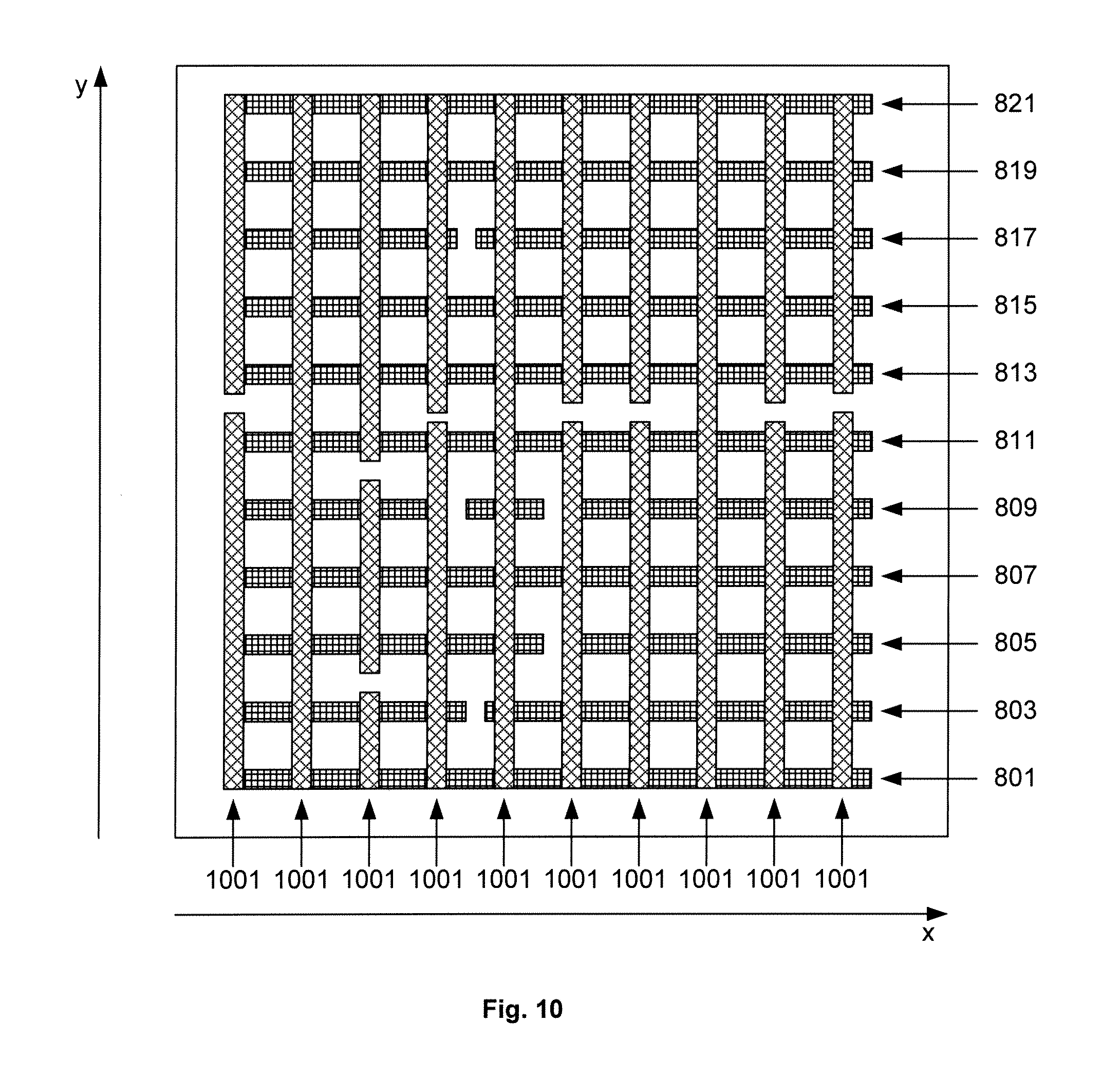
D00014
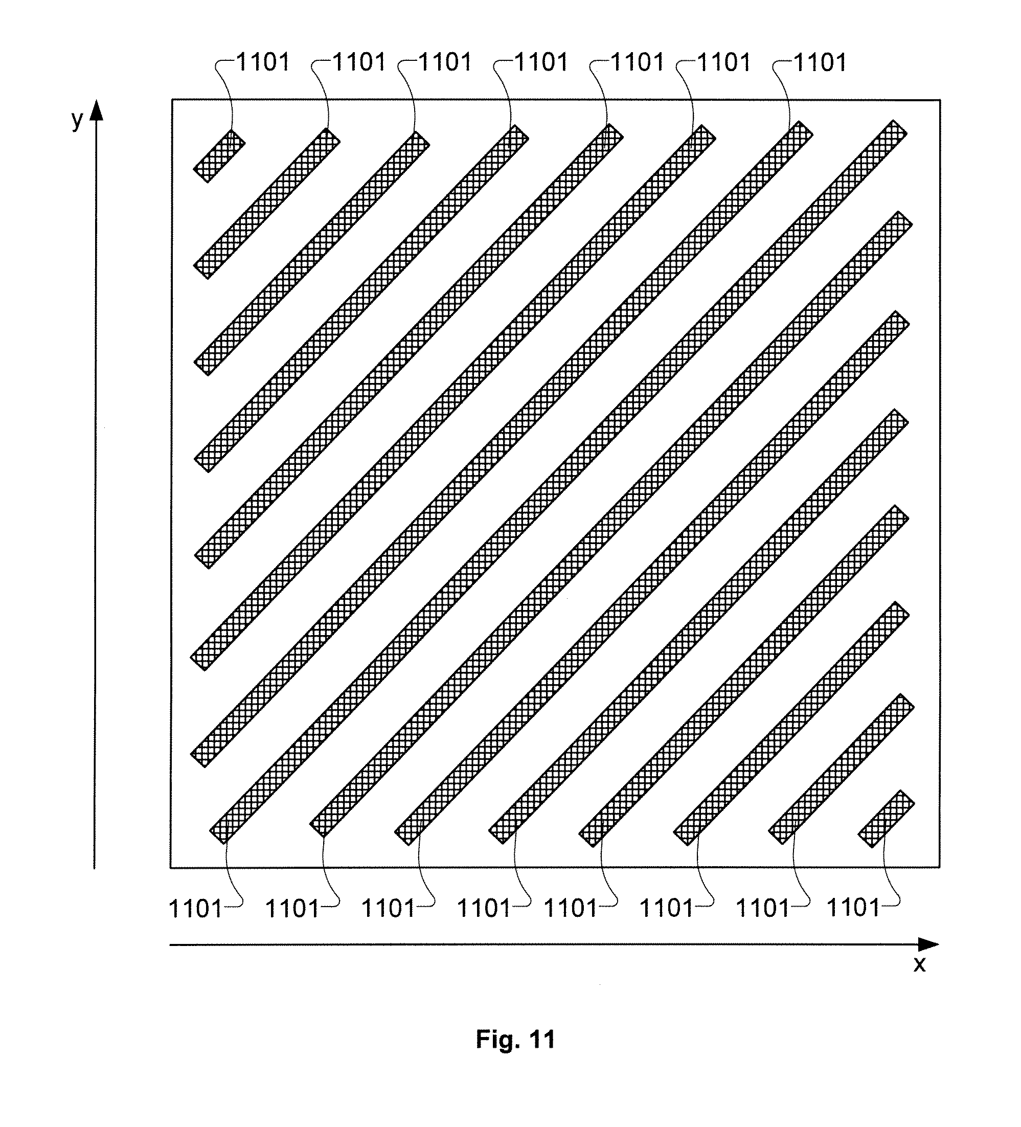
D00015
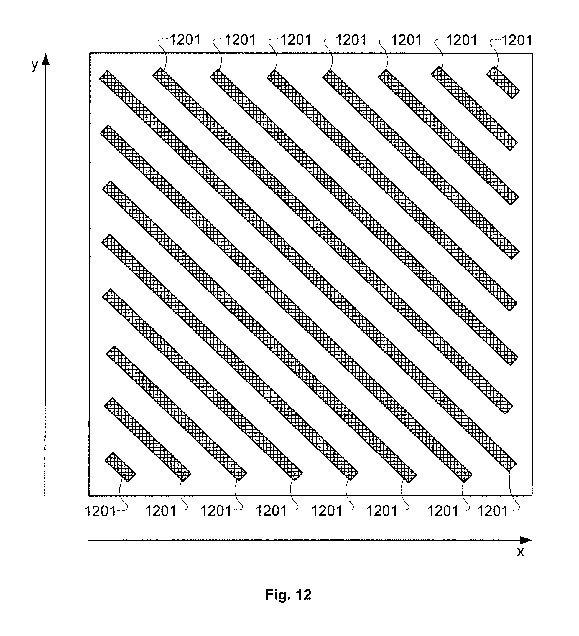
D00016
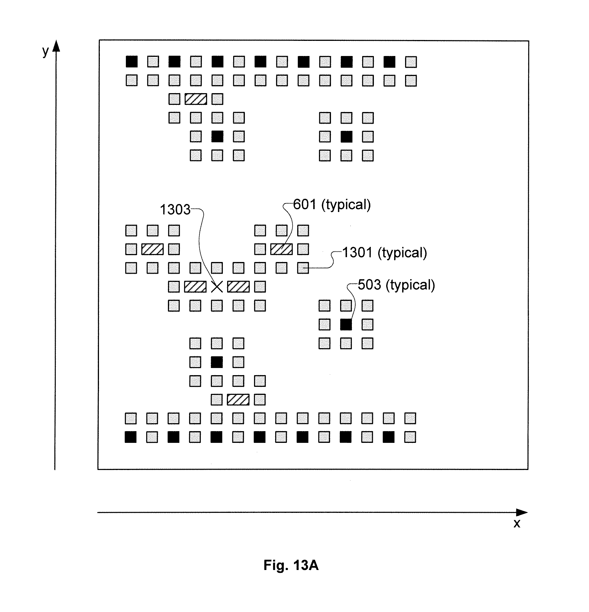
D00017

D00018

D00019

D00020
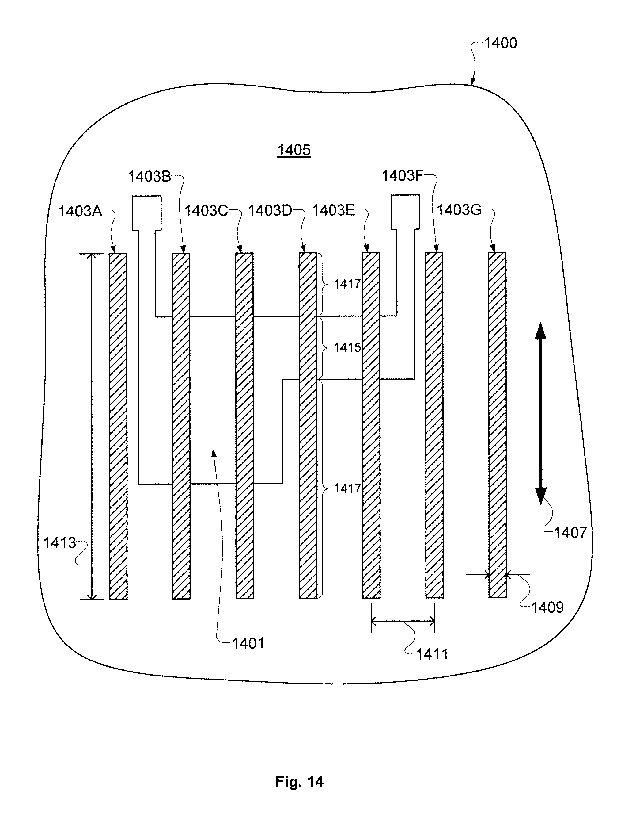
D00021

XML
uspto.report is an independent third-party trademark research tool that is not affiliated, endorsed, or sponsored by the United States Patent and Trademark Office (USPTO) or any other governmental organization. The information provided by uspto.report is based on publicly available data at the time of writing and is intended for informational purposes only.
While we strive to provide accurate and up-to-date information, we do not guarantee the accuracy, completeness, reliability, or suitability of the information displayed on this site. The use of this site is at your own risk. Any reliance you place on such information is therefore strictly at your own risk.
All official trademark data, including owner information, should be verified by visiting the official USPTO website at www.uspto.gov. This site is not intended to replace professional legal advice and should not be used as a substitute for consulting with a legal professional who is knowledgeable about trademark law.