Deposition Method And An Apparatus For Depositing A Silicon-containing Material
Liu; Zecheng ; et al.
U.S. patent application number 17/491684 was filed with the patent office on 2022-04-07 for deposition method and an apparatus for depositing a silicon-containing material. The applicant listed for this patent is ASM IP Holding B.V.. Invention is credited to Zecheng Liu, Viljami Pore, Mikko Ruoho, Tommi Paavo Tynell, Yu Xu.
| Application Number | 20220108915 17/491684 |
| Document ID | / |
| Family ID | 1000005942559 |
| Filed Date | 2022-04-07 |


| United States Patent Application | 20220108915 |
| Kind Code | A1 |
| Liu; Zecheng ; et al. | April 7, 2022 |
DEPOSITION METHOD AND AN APPARATUS FOR DEPOSITING A SILICON-CONTAINING MATERIAL
Abstract
The current disclosure relates to methods of depositing silicon-containing material on a substrate comprising a gap, wherein the method comprises providing the substrate in a reaction chamber and depositing a carbon-containing inhibition layer on the substrate, and depositing silicon-containing material on the substrate. Depositing the inhibition layer comprises supplying a carbon precursor comprising carbon in the reaction chamber and supplying first plasma in the reaction chamber to form a first reactive species from the carbon precursor for forming the inhibition layer on the substrate. The inhibition layer is deposited preferentially in the vicinity of the top of the gap. The disclosure further relates to methods of forming a structure, methods of manufacturing a device and to a semiconductor processing apparatus.
| Inventors: | Liu; Zecheng; (Sagamihara, JP) ; Pore; Viljami; (Helsinki, FI) ; Tynell; Tommi Paavo; (Espoo, FI) ; Xu; Yu; (Vantaa, FI) ; Ruoho; Mikko; (Vantaa, FI) | ||||||||||
| Applicant: |
|
||||||||||
|---|---|---|---|---|---|---|---|---|---|---|---|
| Family ID: | 1000005942559 | ||||||||||
| Appl. No.: | 17/491684 | ||||||||||
| Filed: | October 1, 2021 |
Related U.S. Patent Documents
| Application Number | Filing Date | Patent Number | ||
|---|---|---|---|---|
| 63088276 | Oct 6, 2020 | |||
| Current U.S. Class: | 1/1 |
| Current CPC Class: | H01J 37/32449 20130101; H01L 21/0217 20130101; H01L 21/76837 20130101; H01L 21/0228 20130101; H01L 21/02274 20130101; H01J 37/32146 20130101; H01L 21/02164 20130101; H01J 2237/332 20130101; H01L 21/02205 20130101 |
| International Class: | H01L 21/768 20060101 H01L021/768; H01L 21/02 20060101 H01L021/02; H01J 37/32 20060101 H01J037/32 |
Claims
1. A method of filling a gap with silicon-containing material, wherein the method comprises providing a substrate with the gap in a reaction chamber; supplying a carbon precursor comprising carbon in the reaction chamber; and supplying a first plasma in the reaction chamber to form a first reactive species from the carbon precursor for forming a carbon-containing inhibition layer in a vicinity of a top of the gap; and supplying a first precursor in the reaction chamber to deposit silicon-containing material on the substrate, wherein deposition in the vicinity of the top of the gap is at least partially inhibited by the inhibition layer.
2. The method of claim 1, wherein the carbon precursor comprises a hydrocarbon.
3. The method according to claim 2, wherein the hydrocarbon is an unsubstituted hydrocarbon.
4. The method according to claim 2, wherein the hydrocarbon is a substituted or a functionalized hydrocarbon.
5. The method according to claim 1, wherein the first plasma is produced by gas-phase ionization of a gas with a first radio frequency (RF) power.
6. The method according to claim 1, wherein the first plasma density is tuned to optimize the deposition of the silicon-containing material in predetermined areas of the substrate.
7. The method according to claim 1, wherein the carbon precursor is supplied continuously during the deposition of the inhibition layer.
8. The method according claim 1, wherein supplying the carbon precursor in the reaction chamber at least partially overlaps with supplying first plasma in the reaction chamber.
9. The method according to claim 1, wherein supplying the carbon precursor in the reaction chamber is at least partially separate from supplying first plasma in the reaction chamber.
10. The method according to claim 1, wherein the flow of the carbon precursor is continuous, and the first plasma is supplied in the reaction chamber in two or more pulses.
11. The method according to claim 1, wherein depositing the silicon-containing material on the substrate comprises: supplying a first precursor in the reaction chamber, and supplying a second precursor that reacts with the first precursor in the reaction chamber to form silicon-containing material.
12. The method according to claim 1, wherein the deposition of silicon-containing material is slower on the inhibition layer than on the substrate.
13. The method according to claim 1, wherein the growth of the silicon-containing material on the top surface of a substrate is at least two times slower than at the bottom of the gap.
14. The method according to claim 1, wherein deposition of the silicon-containing material is performed by atomic layer deposition (ALD) process, a plasma enhanced ALD (PEALD) process, chemical vapor deposition (CVD) process or a plasma enhanced chemical vapor deposition (PECVD) process.
15. The method according to claim 1, wherein depositing silicon-containing material on the substrate comprises a cyclic process.
16. The method according to claim 11, wherein the second precursor comprises oxygen.
17. The method according to claim 11, wherein the second precursor comprises one or more of hydrazine (N.sub.2H.sub.4), N.sub.2, Ar/N.sub.2, N.sub.2/H.sub.2, Ar/N.sub.2/H.sub.2 or NH.sub.3.
18. The method according to claim 11, wherein the second precursor comprises plasma.
19. The method according to claim 11, wherein the second precursor at least partially removes the inhibition layer.
20. The method according to claim 1, wherein the deposition of an inhibition layer and/or the deposition of silicon-containing material are performed at least twice.
21. A semiconductor processing apparatus comprising: a reaction chamber for accommodating a substrate; a first source for a carbon precursor in gas communication via a first valve with the reaction chamber; a second source for a second reactant in gas communication via a second valve with the reaction chamber for supplying first plasma; a third source for a first precursor in gas communication via a third valve with the reaction chamber; a fourth source for a second precursor in gas communication via a fourth valve with the reaction chamber; and a controller operably connected to the first, second, third and fourth valves and configured and programmed to control: supplying a carbon precursor in the reaction chamber; and supplying first plasma in the reaction chamber to form a first reactive species from the carbon precursor for forming a carbon-containing inhibition layer; and depositing silicon-containing material on the substrate.
Description
CROSS-REFERENCE TO RELATED APPLICATIONS
[0001] This application claims priority to U.S. Provisional Patent Application Ser. No. 63/088,276 filed Oct. 6, 2020 titled DEPOSITION METHOD AND AN APPARATUS FOR DEPOSITING A SILICON-CONTAINING MATERIAL, the disclosure of which is hereby incorporated by reference in its entirety.
FIELD
[0002] The present disclosure generally relates to methods and apparatuses suitable for manufacturing electronic devices. More particularly, the disclosure relates to methods and apparatuses for depositing silicon-containing material on a substrate and to filling a gap with silicon-containing material during the manufacturing of electronic devices and structures formed using the methods.
BACKGROUND
[0003] Films or layers of material are deposited on a surface of a substrate during manufacturing of electronic devices, such as integrated circuits. During the manufacturing process, gaps, such as recesses, trenches or spaces between elevated portions, such as fins, may be formed. Often, the gaps need to be filled with specific materials to achieve desired device functionalities. In the case of filling a gap, a typical film deposition process may be subjected to drawbacks, including void formation. Such voids may compromise isolation of the devices and the overall structural integrity of the integrated circuit. Dielectric gapfill processes need to be constantly improved as new device architectures place ever more stringent requirements on thermal budgets as well as aspect ratios, spacing, and shapes of gaps.
[0004] Using conventional techniques, such as conventional plasma-enhanced chemical vapor deposition to fill gaps, can result in poor film quality (for example a relatively high (e.g., wet) etch rate), seam formation, and/or void formation. Seams and voids that form within deposited material within the recess can be problematic in several regards. For example, seams and/or voids formed within material deposited in recesses that are used for shallow trench isolation (STI) can result in unwanted parasitic current. Further, the voids and seams can cause problems during subsequent processes, such as chemical mechanical polishing and etching.
[0005] Void formation may be mitigated by decreasing gap depth and/or tapering gap sidewalls, so that the openings of the recess are wider at the top than at the bottom of the recess. However, such solutions may reduce the effectiveness of device isolation, and/or be incompatible with the need to reduce device dimensions.
[0006] Recently, plasma-enhanced atomic layer deposition (PEALD) techniques have been developed to deposit material into a gap more conformally. However, techniques to fill gaps using PEALD, particularly techniques to provide filling of high aspect ratio (e.g., aspect ratios greater than 15 or even 30) gaps with high-quality dielectric material, such as silicon oxide that exhibits a relatively low (e.g., less than about 4.5 nm/min) wet etch rate (e.g., a wet etch rate ratio of about 1.8) in 0.5% diluted HF solution has, to date, been challenging. Further, filling reentrant gaps (gaps with an opening diameter that may be smaller than a diameter of the recess at the bottom area of the recess) has proven to be difficult using typical PEALD techniques. Accordingly, improved methods and apparatuses for gap filling are desired.
SUMMARY
[0007] This summary may introduce a selection of concepts in a simplified form, which may be described in further detail below. This summary is not intended to necessarily identify key features or essential features of the claimed subject matter, nor is it intended to be used to limit the scope of the claimed subject matter.
[0008] Conformal processes with good step coverage and low-viscosity dielectric materials have offered solutions for gapfill problems in the past, but the ideal gapfill process would produce film growth from the bottom of the gap upwards, filling the gap without the need for subsequent planarization steps. In this disclosure, the deposition process is modified so that growth is inhibited in the vicinity of a top of a gap, which may result in faster and/or preferred growth within the gap.
[0009] Embodiments of the present disclosure relate to methods of depositing silicon-containing material on a substrate comprising a gap, methods of filling a gap, methods of forming a semiconductor device. Further, embodiments of the current disclosure relate to semiconductor processing apparatuses. The embodiments of the methods and apparatuses according to the current disclosure may be suitable for filling high aspect ratio gaps with desired material, such as dielectric material. As set forth in more detail below, exemplary methods can inhibit deposition of material at, or in the vicinity of a top of a gap, relative to a bottom of the gap, to facilitate filling of the gap. In some embodiments, the filling of a gap may be seamless. Examples of the disclosure may allow for low-temperature deposition of material, which can reduce oxidation of underlying and/or surrounding material. Additionally, high-quality deposited material can be formed within the gap, in some embodiments without post-treatment annealing of the deposited material that is otherwise often performed to improve the quality of recess fill material.
BRIEF DESCRIPTION OF DRAWINGS
[0010] The accompanying drawings, which are included to provide a further understanding of the disclosure and constitute a part of this specification, illustrate exemplary embodiments, and together with the description help to explain the principles of the disclosure. In the drawings:
[0011] FIG. 1 depicts an embodiment of the method according to the current disclosure.
[0012] FIG. 2 illustrates an embodiment of a gap being filled according to the current disclosure.
[0013] FIG. 3 is a schematic representation of an apparatus according to the current disclosure.
[0014] Elements in the figures are illustrated for simplicity and clarity and have not necessarily been drawn to scale. For example, the dimensions of some of the elements in the figures may be exaggerated relative to other elements to help improve understanding of illustrated embodiments of the present disclosure.
DETAILED DESCRIPTION OF EXEMPLARY EMBODIMENTS
[0015] The description of exemplary embodiments of methods, structures, devices and apparatuses provided below is merely exemplary and is intended for purposes of illustration only. The following description is not intended to limit the scope of the disclosure or the claims. Moreover, recitation of multiple embodiments having stated features is not intended to exclude other embodiments having additional features or other embodiments incorporating different combinations of the stated features. For example, various embodiments are set forth as exemplary embodiments and may be recited in the dependent claims.
[0016] It will be understood by those in the art that the invention extends beyond the specifically disclosed embodiments and/or uses of the invention and obvious modifications and equivalents thereof. Thus, it is intended that the scope of the invention disclosed should not be limited by the particular disclosed embodiments described below. Unless otherwise noted, the exemplary embodiments or components thereof may be combined or may be applied separate from each other.
[0017] In this disclosure, any two numbers of a variable can constitute a workable range of the variable, and any ranges indicated may include or exclude the endpoints. Additionally, any values of variables indicated (regardless of whether they are indicated with "about" or not) may refer to precise values or approximate values and include equivalents, and may refer to average, median, representative, majority, or the like.
[0018] Exemplary embodiments of the disclosure can be used to fill gaps, such as trenches, vias, and/or areas between fins on a surface of a substrate. By way of particular example, exemplary methods can be used for shallow trench isolation (STI) applications in the manufacture of electronic devices, such as memory and/or logic circuits. For example, in embodiments where the silicon-containing material comprises, consist essentially of, or consist of silicon oxide, current methods, structures and devices according to the current disclosure may be used for PMD gapfill for memory and logic and/or for high aspect ratio gapfill for 3D NAND and/or for buried power rail oxide gapfill. For example, in embodiments where the silicon-containing material comprises, consist essentially of, or consist of silicon nitride, current methods, structures and devices according to the current disclosure may be used for SNC gapfill for DRAM, SAC gapfill and gapfill for forksheet transistors.
[0019] In one aspect, a method of filling a gap with silicon-containing material is disclosed. The method comprises providing a substrate with the gap in a reaction chamber, supplying a carbon precursor comprising carbon in the reaction chamber and supplying a first plasma in the reaction chamber to form a first reactive species from the carbon precursor. Thus, a carbon-containing inhibition layer is formed in a vicinity of a top of the gap. Further, in the method, a first precursor is supplied in the reaction chamber to deposit silicon-containing material on the substrate, and the deposition in the vicinity of the top of the gap is at least partially inhibited by the inhibition layer.
[0020] The vicinity of the top of the gap is the area extending inside and outside of the gap. By the top of the gap is herein meant the area of the gap opening and the surface of the substrate surrounding it. The top of the gap can be considered being the complete upmost surface of the substrate. Thus, the inhibition layer may be formed in substantially all other parts of the substrate surface, except on the inside of the gap and some length into the gap. The depth into which the inhibition layer may extend in the gap depends on the process conditions used, and may be regulated according to the specific application.
[0021] Thus, a method of depositing silicon-containing material on a substrate comprising a gap is disclosed. The silicon-containing material may be deposited primarily in a gap, and to a lesser extent on the top surface of the substrate. The silicon-containing material may be deposited substantially only in a gap. In some embodiments, silicon-containing material may be deposited only in a gap.
[0022] The silicon-containing material may comprise substantially only silicon oxide, such as SiO.sub.2. In some embodiments, the silicon-containing material may consist essentially of, or consist of silicon oxide. The silicon-containing material may comprise boron-doped silicon oxide, phosphorus-doped silicon oxide, silicon, poly-silicon, silicon carbides, and silicon nitrides. In some embodiments, the silicon-containing material may comprise substantially only silicon nitride. In some embodiments, the silicon-containing material may consist essentially of, or consist of silicon nitride.
[0023] Thus, the method comprises providing the substrate with a gap in a reaction chamber, depositing a carbon-containing inhibition layer on the substrate and depositing silicon-containing material in the gap. In the method, the carbon-containing inhibition layer is formed by supplying a carbon precursor comprising carbon in the reaction chamber and supplying first plasma in the reaction chamber to form a first reactive species from the carbon precursor. A plasma reactant is used for forming first plasma.
[0024] The inhibition layer is deposited in the vicinity of the top of the gap. The inhibition layer may extend along the top surface of the substrate. Thus, the inside of the gap away from the top of the gap may be the only surface in which there is no inhibition layer. Substantially all of the top surface of the substrate may contain the inhibition layer. By the inhibition layer being deposited in the vicinity of the top of the gap is thus meant deposition taking place inside the gap.
[0025] The method of depositing silicon-containing material according to the current disclosure comprises providing a substrate in a reaction chamber. In other words, a substrate is brought into space where the deposition conditions can be controlled. The reaction chamber may be part of a cluster tool in which different processes are performed to form an integrated circuit. In some embodiments, the reaction chamber may be a flow-type reactor, such as a cross-flow reactor. In some embodiments, the reaction chamber may be a showerhead reactor. In some embodiments, the reaction chamber may be a space-divided reactor. In some embodiments, the reaction chamber may be single wafer ALD reactor. In some embodiments, the reaction chamber may be a high-volume manufacturing single wafer ALD reactor. In some embodiments, the reaction chamber may be a batch reactor for manufacturing multiple substrates simultaneously.
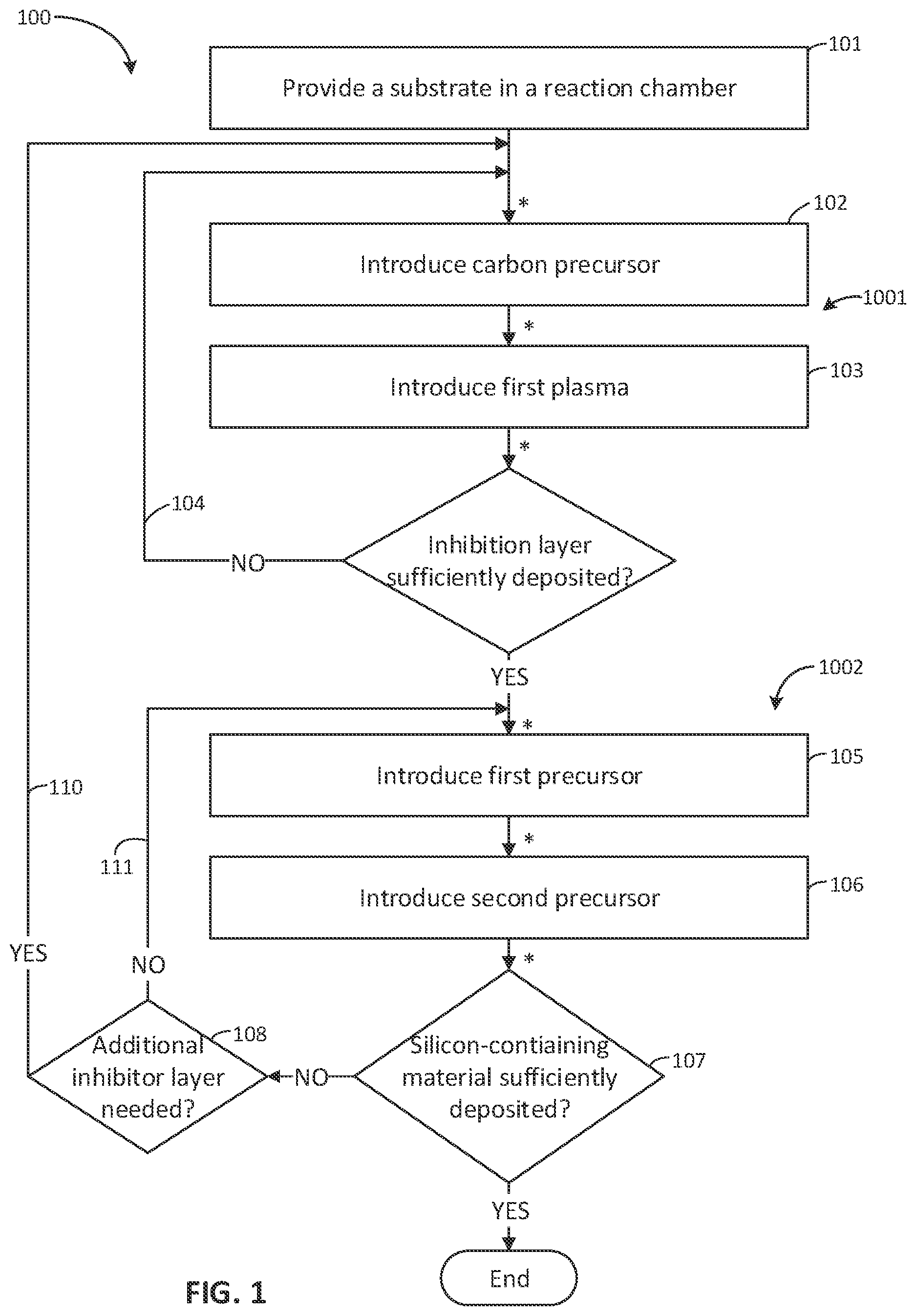
[0026] In another aspect, a method of forming a structure is disclosed. The method comprises filling a gap with silicon-containing material by providing the substrate comprising a gap in a reaction chamber, depositing a carbon-containing inhibition layer on the substrate and depositing silicon-containing material on the substrate. In the method, the carbon-containing inhibition layer is formed by supplying a carbon precursor comprising carbon in the reaction chamber and supplying first plasma in the reaction chamber to form a first reactive species from the carbon precursor, wherein the inhibition layer is deposited in the vicinity of the top of the gap. An aspect of the current disclosure is a structure formed according to methods described herein.
[0027] In yet another aspect, a method of forming a semiconductor device is disclosed. The method of forming a semiconductor device according to the current disclosure comprises filling a gap with silicon-containing material by providing the substrate comprising a gap in a reaction chamber, depositing a carbon-containing inhibition layer on the substrate and depositing silicon-containing material on the substrate. In the method, the carbon-containing inhibition layer is formed by supplying a carbon precursor comprising carbon in the reaction chamber and supplying first plasma in the reaction chamber to form a first reactive species from the carbon precursor, wherein the inhibition layer is deposited in the vicinity of the top of the gap. An aspect of the current disclosure is a device formed according to methods described herein.
[0028] As used herein, the term substrate may refer to any underlying material or materials that may be used to form, or upon which, a device, a circuit, or a material layer may be formed. A substrate can include a bulk material, such as silicon (e.g., single-crystal silicon) and can include one or more layers overlying the bulk material. The substrate can include various topologies, such as gaps, including recesses, lines, trenches or spaces between elevated portions, such as fins, and the like formed within or on at least a portion of a layer of the substrate. Substrate may include nitrides, for example TiN, oxides, insulating materials, dielectric materials, conductive materials, metals, such as such as tungsten, ruthenium, molybdenum or copper, or metallic materials, crystalline materials, epitaxial, heteroepitaxial, and/or single crystal materials. In some embodiments of the current disclosure, the substrate comprises silicon. The substrate may comprise other materials, as described above, in addition to silicon. The other materials may form layers.
[0029] A gap in this disclosure is in or on a substrate. It is intended to mean changes in the surface topology of the substrate leading to some areas of the substrate surface being lower than other areas. Gaps thus include topologies in which parts of the substrate surface are lower relative to the majority of the substrate surface. These include trenches, vias, recesses, valleys, crevices and the like. Further, also areas between elevated features protruding upwards of the majority of the substrate surface form gaps. Thus, the space between adjacent fins is considered a gap.
[0030] The gap may have tapered or slanting walls, narrowing the diameter of the gap either towards the top or towards the bottom of the gap. The tapering or slanting may cause the gap opening to have larger surface area than the gap bottom. Alternatively, the tapering may cause the gap opening to have smaller surface area than the gap bottom. Especially gaps having a smaller surface area than the gap bottom may be challenging to fill without void formation.
[0031] In some embodiments, the width of the gap may be from about 3 nm to about 400 nm. For example, the width of the gap may be from about 4 nm to about 300 nm, from about 5 nm to about 100 nm, from about 10 nm to about 50 nm, or about 20 nm. In some embodiments, the width of the gap may be from about 100 nm to about 400 nm, such as about 150 nm, 200 nm, 250 nm, 300 nm or 350 nm. In other embodiments, the width of the gap may be from about 3 nm to about 50 nm, such as from about 3 nm to 10 nm, from about 3 nm to 20 nm, from about 3 nm to about 30 nm, from about 3 nm to about 40 nm. As an example, the width of the gap may be about 4 nm, about 5 nm, about 6 nm, about 8 nm or about 12 nm, about 15 nm, about 18 nm, about 25 nm or about 35 nm.
[0032] In some embodiments, the depth of the gap is from about 50 nm to about 7 .mu.m, or about 10 .mu.m. Examples of applications in which the depth of the gap may be in the micrometer range, may include VNADN applications, or other circumstances in which a hole is etched through a stack. Such etching may take place in one or more, such a two steps. For example, the depth of the gap may be from about 50 nm to about 4 .mu.m, from about 50 nm to about 2 .mu.m, from about 50 nm to about 1 .mu.m or from about 50 nm to about 500 nm. In additional examples, the depth of gap may be from about 50 nm to about 200 nm, from about 50 nm to about 200 nm, or from about 200 nm to about 7 .mu.m, from about 200 nm to about 5 .mu.m, from about 200 nm to about 3 .mu.m, from about 200 nm to about 1 .mu.m, or from about 200 nm to about 500 nm.
[0033] In some embodiments, the width to depth aspect ratio of the gap is between approximately 1:0.5 to 1:250. In certain embodiments, the width to depth aspect ratio of the gap is between approximately 1:1 to 1:200, between approximately 1:1 to 1:100, between approximately 1:0.5 to 1:50, such as 1:2, 1:3, 1:5, 1:8, 1:10, 1:20, 1:50, or 1:150.
[0034] By deposition in the current disclosure is meant depositing material on the substrate using chemical vapor deposition (CVD), plasma-enhanced CVD (PECVD), physical vapor deposition (PVD), atomic layer deposition (ALD) or plasma-enhanced ALD (PEALD). In some embodiments, the carbon-containing inhibitor according to the current disclosure is deposited using PECVD. In some embodiments, the silicon-containing material is deposited using ALD. In some embodiments, the silicon-containing material is deposited using PEALD.
[0035] CVD processes may involve gas phase reactions between two or more reactants. The reactants can be provided simultaneously to the reaction chamber or substrate, or in partially or completely separated pulses (cyclic CVD). The substrate and/or reaction chamber can be heated to promote the reaction between the gaseous reactants. A PECVD process may comprise only one reactant, which is exposed to plasma to increase its reactivity and/or chemisorption to the substrate surface. In some embodiments the reactant(s) and possible plasma are provided until a layer having a desired thickness is deposited.
[0036] As used herein, ALD may refer to a vapor deposition process in which deposition cycles, such as a plurality of consecutive deposition cycles, are conducted. ALD is based on controlled, often self-limiting surface reactions of the precursor chemicals. Gas phase reactions are avoided by feeding the precursors alternately and sequentially into the reaction chamber. Generally, during each cycle, a first precursor is chemisorbed to a deposition surface (e.g., a substrate surface that can include a previously deposited material from a previous ALD cycle or other material), forming about a monolayer or sub-monolayer of material that does not readily react with additional first precursor. Thereafter, in some cases, a second precursor or reaction gas may subsequently be introduced into the reaction chamber for use in converting the chemisorbed precursor to the desired material on the deposition surface. Vapor phase reactants are separated from each other in the reaction chamber, for example, by removing excess reactants and/or reactant by-products from the reaction chamber between reactant pulses. This may be accomplished with an evacuation step and/or with an inactive gas pulse or purge. In some embodiments the substrate is contacted with a purge gas, such as an inert gas. For example, the substrate may be contacted with a purge gas between reactant pulses to remove excess reactant and reaction by-products.
[0037] In some embodiments each reaction is self-limiting and monolayer by monolayer growth is achieved. These may be referred to as "true ALD" reactions. In some such embodiments the first precursor may adsorb on the substrate surface in a self-limiting manner. A second precursor will react in turn with the adsorbed first precursor to form up to a monolayer of material on the substrate.
[0038] Further, the term atomic layer deposition, as used herein, may also be meant to include processes designated by related terms, such as chemical vapor atomic layer deposition, atomic layer epitaxy (ALE), molecular beam epitaxy (MBE), gas source MBE, or organometallic MBE, and chemical beam epitaxy when performed with alternating pulses of precursor(s)/reactive gas(es), and purge (e.g., inert carrier) gas(es).
[0039] In the current disclosure, a carbon-containing inhibition layer is deposited on the surface of the substrate. The inhibition layer is deposited on, and in the vicinity of, the topmost areas of the substrate. The inhibition layer may extend downwards into the gap. The depth of the deposition in the gap may be influenced through the process conditions, such as plasma power. The properties of the inhibition layer may be influenced through the process conditions. The skilled person may take the topology of the substrate into account in selecting of the process conditions to obtain the desired result. In some embodiments, there is substantially no deposition of the inhibition layer at the bottom of the gap.
[0040] In the current disclosure, the inhibition layer is formed by supplying a carbon precursor comprising carbon in the reaction chamber and supplying first plasma in the reaction chamber to form a first reactive species from the carbon precursor. The carbon precursor may be supplied in the reaction chamber simultaneously with supplying first plasma in the reaction chamber. Thus, in some embodiments, supplying carbon precursor in a reaction chamber at least partially overlaps with supplying first plasma in the reaction chamber. In some embodiments, supplying carbon precursor in a reaction chamber is at least partially separated from supplying first plasma in the reaction chamber. In some embodiments, providing a carbon precursor into the reaction chamber is started before the first plasma is switched on (i.e. providing the first plasma is started). In some embodiments, providing a carbon precursor into the reaction chamber is ended at the same time when plasma is turned off. In some embodiments, the generation of first plasma is initiated before a carbon precursor is provided into the reaction chamber. In such embodiments, the first plasma and the second plasma may be the same, and the first plasma generated before a carbon precursor is provided into the reaction chamber may function as the second plasma for a first precursor provided into the reaction chamber during the previous deposition cycle. In some embodiments, supplying carbon precursor in a reaction chamber is simultaneous with supplying first plasma in the reaction chamber. In some embodiments, supplying carbon precursor in a reaction chamber is substantially completely, or completely separated from supplying first plasma in the reaction chamber. The carbon precursor may be supplied in the reaction chamber partially simultaneously with supplying first plasma in the reaction chamber.
[0041] In some embodiments, a gas, such as argon and/or hydrogen, from which the first plasma is generated is continuously provided into the reaction chamber. In some embodiments, when the silicon-containing material comprises nitrogen (such as SiN, SiCN), nitrogen gas may be continuously provided into the reaction chamber. In some embodiments, a carbon precursor may be continuously provided into the reaction chamber. In such embodiments, the carbon precursor does preferentially not react with the first precursor. Continuous-flow embodiments described above may have the advantage of improving process throughput.
[0042] The reaction chamber may be purged after supplying carbon precursor and before supplying plasma, and/or after supplying plasma and before supplying carbon precursor. During purging the reaction chamber, excess precursor(s) and reaction byproducts, if any, may be removed from the reaction chamber and/or substrate surface. For example, a purging gas pulse and/or vacuum generated by a pumping system may be used in purging the reaction chamber. The purging gas can be any inert gas, such as, without limitation to, argon (Ar), nitrogen (N.sub.2) and/or helium (He). A flowrate of a purging gas during purging the reaction chamber and/or substrate surface may range from about 500 sccm to about 4500 sccm or about 2000 sccm to about 4000 sccm.
[0043] In some embodiments, the carbon precursor may be continuously supplied to the reaction chamber, whereas first plasma may be supplied into the reaction chamber in pulses. The pulse time for plasma may be 0.2 s to 3 s, for example 0.5 s, 0.7 s, 1 s, 1.3 s, 1.5 s. 2 s or 2.5 s. The purge time between plasma pulses may be between 0.1 s and 2 s, for example 0.2 s, 0.3 s, 0.5 s, 0.7 s, 1 s or 1.5 s. Alternatively or in addition, first plasma may be continuously supplied to the reaction chamber, whereas the carbon precursor may be supplied into the reaction chamber in pulses. The pulse time for the carbon precursor may be between 0.1 s and 2.5 s, for example 0.2 s, 0.3 s, 0.5 s, 1 s, 1.5 s or 2 s. There may be a purge time of 0.1 s to 2 s, for example 0.2 s, 0.3 s, 0.5 s, 0.7 s, 1 s or 1.5 s between carbon precursor pulses. In some embodiments, both the carbon precursor and the first plasma are supplied in pulses. After one or more carbon precursor pulses, one or more first plasma pulses may be applied.
[0044] First plasma and carbon precursor may be supplied in the reaction chamber in an alternating manner. In some embodiments, supplying the carbon precursor and/or supplying the first plasma are performed at least twice, such as at least three times, at least five times or at least ten times. In some embodiments, the flow of the carbon precursor is continuous, and the first plasma is supplied in the reaction chamber in two or more pulses. For example, the number of plasma pulses may be three, five or ten times before silicon-containing material is deposited. In some embodiments, supplying the carbon precursor in the reaction chamber is at least partially separate from supplying first plasma in the reaction chamber. In some embodiments, there is no overlap between supplying the carbon precursor in the reaction chamber and supplying first plasma in the reaction chamber.
[0045] As used herein, the term film or layer can refer to any continuous or non-continuous deposit and material, such as material deposited by the methods disclosed herein. For example, film or layer can include two-dimensional materials, three-dimensional materials, nanoparticles or even partial or full molecular layers or partial or full atomic layers or clusters of atoms and/or molecules. A film or layer may comprise material or a layer with pinholes, which may be at least partially continuous. In some embodiments, the inhibition layer may be continuous. In some embodiments, the inhibition layer may be substantially continuous. In some embodiments, the thickness of the inhibition layer at the top of the substrate may be between approximately 0.1 nm to 10 nm. For example, the thickness of the inhibition layer may be between 0.5 nm and 8 nm, or between 0.2 nm and 8 nm, or between 1 nm and 8 nm, or between 0.5 nm and 5 nm. The thickness of an inhibition layer may vary in different areas of the substrate. For example, inhibition layer on the top surface of the substrate may be thicker than in a gap. The thickness of an inhibition layer may gradually decrease towards the bottom of a gap. For example, the inhibition layer may be absent from the bottom of a gap, whereas the thickness of the inhibition layer may be, for example, 1 nm, 3 nm, 5 nm, 7 nm or 9 nm at the top surface of the substrate.
[0046] In some embodiments, the inhibition layer is deposited substantially only on the top surface of the substrate. In some embodiments, the inhibition layer extends into the gap. In some embodiments, the inhibition layer extends into the gap for half of the depth of the gap at most, or for one third of the depth of the gap at most. In some embodiments, the inhibition layer extends into the gap for at least 5 nm, or at least 10 nm, or at least 50 nm. In some embodiments, the inhibition layer may extend into the gap for at least 100 nm, or at least 250 nm, or at least 300 nm or at least 500 nm. In some embodiments, the inhibition layer extends into the gap substantially along the entire depth of the gap.
[0047] In some embodiments, the carbon precursor comprises a hydrocarbon. In some embodiments, the carbon precursor comprises substantially only one or more hydrocarbons. In some embodiments, the carbon precursor comprises two or more compounds. The carbon precursor may comprise a mixture of isomers of a compound.
[0048] The hydrocarbon may comprise 1 to 10 carbon atoms, the hydrocarbon may comprise 2 to 8 carbon atoms or the hydrocarbon may comprise 1 to 5 carbon atoms, such as 3 or 4 carbon atoms. The hydrocarbon may comprise 6 to 10 carbon atoms, such as 7 or 9 carbon atoms. The hydrocarbon may comprise more carbon atoms, such as 10 to 20 carbon atoms, for example, 11, 12, 14 or 16 carbon atoms.
[0049] The hydrocarbon may be aliphatic or aromatic. The hydrocarbon may be saturated or unsaturated, linear or branched, cyclic or acyclic. In some embodiments, the hydrocarbon is an unsubstituted hydrocarbon, i.e., it comprises only carbon and hydrogen. In some embodiments, the hydrocarbon is a substituted or a functionalized hydrocarbon. For example, the hydrocarbon may be a halogenated hydrocarbon, such as a chlorinated hydrocarbon, a fluorinated hydrocarbon, a brominated hydrocarbon, or a iodinated hydrocarbon. The hydrocarbon may be a hydroxylated hydrocarbon, an alcohol, or a carboxylic acid. The hydrocarbon may be an ester, a ketone or an aldehyde. The hydrocarbon may comprise an amine or an imine.
[0050] In some embodiments, the carbon precursor comprises one or more of methane, ethane, propane, butane, pentane, hexane, heptane, octane, acetylene, benzene, toluene, ethylenediamine (EDA), diethylamine (DEA), tert-butylamine (TBA), or derivatives thereof.
[0051] In the current disclosure, the carbon-containing inhibition layer may be formed by supplying a carbon precursor in the reaction chamber and contacting it with plasma. The plasma may cause first reactive species to be formed from the carbon precursor. The first reactive species may be deposited on the surface of the substrate. The first reactive species deposited on the surface of the substrate may form the inhibition layer. In some embodiments, the first plasma is selected from a group consisting of nitrogen (N.sub.2) plasma, argon (Ar) plasma, helium (He) plasma, neon (Ne) plasma, krypton (Kr) plasma, and xenon (Xe) plasma and any combination thereof. In some embodiments, the first plasma may comprise oxygen. In some embodiments, the first reactive species is formed using direct plasma, or wherein the first reactive species is formed using remote plasma.
[0052] In some embodiments, the first plasma is produced by gas-phase ionization of a gas with a first radio frequency (RF) power. In some embodiments, the first RF power is between 20 W and 2 kW. For example, the first RF power may be 50 W, 100 W, 200 W, 400 W, 500 W, 700 W, 1 kW, 1.4 kW or 1.8 kW.
[0053] Adjusting the power of the RF plasma generator during the deposition of the inhibition layer may affect the coverage of the inhibition layer, and/or how deep into a gap the inhibition layer reaches. Without limiting the current invention to any specific theory, higher RF power may lead to inhibition of silicon-containing material deposition more effectively and deeper inside a gap. Therefore, depending on the application, a lower RF power may lead to faster gap filling, and thicker silicon-containing material deposition on the top of the surface topology, whereas a higher RF power could be chosen if the aspect ratio is high and growth of the silicon-containing material on the top of the surface topology needs to be avoided.
[0054] In some embodiments, the method further comprises supplying inert gas to the reaction chamber. An inert gas may be used to provide a protective atmosphere for the substrate before and after depositing material on the substrate. An inert gas may be used to purge the reaction chamber of precursor(s) and/or reaction by-products, for example. An inert gas can be used to regulate the flow of precursor(s) and/or precursors. Thus, the precursor concentration and residence time in the reaction chamber can be adjusted. Such a gas may be called a carrier gas. In some embodiments, the method comprises supplying carrier gas in the reaction chamber. The term inert gas (including a carrier gas) can refer to a gas that does not take part in a chemical reaction and/or does not become a part of the deposited material to an appreciable extent. Exemplary inert gases include He and Ar and any combination thereof. In some cases, nitrogen and/or hydrogen can be an inert gas. However, in some embodiments, in addition to being used as an inert gas, nitrogen gas may be used to produce plasma for depositing the silicon-containing material, such as silicon nitride. In some embodiments, the first plasma is at least partially produced from the carrier gas. In some embodiments, the first plasma is substantially produced from the carrier gas. In some embodiments, the carrier gas is Ar and it is used to produce the first plasma. In some embodiments, the plasma is produced from a gas other than the carrier gas.
[0055] In some embodiments, the first plasma density is tuned to optimize the deposition of the silicon-containing material in predetermined areas of the substrate. The plasma density may be tuned to regulate how deep into the gap the inhibition layer is deposited. With higher plasma density, the inhibition layer may be deposited deeper into the gap than with lower plasma density, when other process variables remain same or similar.
[0056] In some embodiments, the method is performed at a temperature of approximately 75.degree. C. to 550.degree. C. The method may be performed at a temperature lower than or equal to 450.degree. C., or lower than or equal to 400.degree. C., or lower than or equal to 350.degree. C., or lower than or equal to 250.degree. C. In some embodiments, temperature may be indicated as the temperature of the reaction chamber or as the temperature of the susceptor. Alternatively, in some embodiments, the temperature may be indicated as the temperature of the substrate or as the temperature of the gas(es) supplied in the reaction chamber. Different stages of the method according to the current disclosure may performed in different temperatures.
[0057] In some embodiments, the inhibition layer is deposited at the same temperature as the silicon-containing material. In some embodiments, the inhibition layer is deposited at a different temperature than the silicon-containing material. In some embodiments, the inhibition layer is deposited at a lower temperature than the silicon-containing material. In some embodiments, the inhibition layer is deposited at a higher temperature than the silicon-containing material.
[0058] In some embodiments, the pressure of the reaction chamber during supplying the carbon precursor and/or the first plasma is below 100 Torr, or below 50 Torr, or below 10 Torr, or below 1 Torr, or below 0.5 Torr or below 0.1 Torr.
[0059] When at least some inhibition layer has been deposited on the substrate, silicon-containing material is deposited on the substrate. In some embodiments, the deposition of silicon-containing material is slower on a substrate comprising an inhibition layer than on the substrate not containing an inhibition layer. The growth of silicon-containing material on the inhibition layer may be, for example, from two times to one thousand times slower than on the substrate that does not contain an inhibition layer. For example, the growth of the silicon-containing material may be three times, four times, five times, ten times, twenty times, fifty times or hundred times slower on a substrate comprising an inhibition layer than on the substrate that does not contain an inhibition layer. In some embodiments, the growth of the silicon-containing material on a substrate comprising an inhibition layer is two hundred or five hundred times slower than on a substrate not comprising an inhibition layer. In some embodiments, the growth of the silicon-containing material on a substrate comprising an inhibition layer is non-detectable.
[0060] In some embodiments, the growth of the silicon-containing material on the top surface of a substrate is at least two times slower than at the bottom of the gap. In some embodiments, the growth of the silicon-containing material on the top surface of a substrate is at least five times slower than at the bottom of the gap. In some embodiments, the growth of the silicon-containing material on the top surface of a substrate is at least ten times slower than at the bottom of the gap. In some embodiments, the growth of the silicon-containing material on the top surface of a substrate is at least fifty times slower than at the bottom of the gap. In some embodiments, the growth of the silicon-containing material on a substrate comprising an inhibition layer is non-detectable.
[0061] In some embodiments, the thickness of the silicon-containing material on the top surface of the substrate is smaller than in the gap. Is some embodiments, the thickness of the silicon-containing material on the top surface of the substrate is at least two times smaller than in the gap. In some embodiments, the thickness of the silicon-containing material on the top surface of the substrate is at least five times smaller than in the gap. In some embodiments, the thickness of the silicon-containing material on the top surface of the substrate is at least ten times smaller than in the gap. In some embodiments, the silicon-containing material on the top surface of a substrate is non-detectable.
[0062] In some embodiments, depositing silicon-containing material on the substrate comprises a cyclic process. In some embodiments, deposition of the silicon-containing material is performed by atomic layer deposition (ALD) process, a plasma enhanced ALD (PEALD) process, chemical vapor deposition (CVD) process or a plasma enhanced chemical vapor deposition (PECVD). In some embodiments, the silicon-containing material may form a layer.
[0063] In some embodiments, the silicon-containing material substantially fills a gap in the substrate. In some embodiments, the gap may be filled seamlessly.
[0064] In some embodiments, depositing silicon-containing material on the substrate comprises supplying a first precursor in the reaction chamber, and supplying a second precursor that reacts with the first precursor in the reaction chamber to form silicon-containing material. In some embodiments, the silicon-containing material comprises silicon oxide, such as silicon dioxide (SiO.sub.2).
[0065] In some embodiments, the first precursor is a silicon-containing precursor. In some embodiments, the first precursor comprises one or more of a silane, aminosilane, iodosilane, a siloxane amine, a silazane amine and silicon halide or a combination thereof. In some embodiments, the first precursor comprises at least one of DIPAS, SiH.sub.3N(iPr).sub.2, TSA, (SiH.sub.3).sub.3N, DSO, (SiH.sub.3).sub.2, DSMA, (SiH.sub.3).sub.2NMe, DSEA, (SiH.sub.3).sub.2Net, DSIPA, (SiH.sub.3)2N(iPr), DSTBA, (SiH.sub.3).sub.2N(tBu), DEAS, SiH.sub.3NEt.sub.2, DTBAS, SiH.sub.3N(tBu).sub.2, BDEAS, SiH.sub.2(NEt.sub.2).sub.2, BDMAS, SiH.sub.2(NMe.sub.2).sub.2, BTBAS, SiH.sub.2(NHtBu).sub.2, BITS, SiH.sub.2(NHSiMe.sub.3).sub.2, TEOS, Si(OEt).sub.4, SiCl.sub.4, HCD, Si.sub.2Cl.sub.6, 3DMAS, SiH(N(Me).sub.2).sub.3, BEMAS, SiH.sub.2[N(Et)(Me)].sub.2, AHEAD, Si.sub.2(NHEt).sub.6, TEAS, Si(NHEt).sub.4, Si.sub.3H.sub.8, DCS, SiH.sub.2Cl.sub.2, SiHI.sub.3, SiH.sub.2I.sub.2 or a combination thereof. As a particular example, the first precursor can be or include a silanediamine, such as N,N,N',N'-tetraethyl silanediamine.
[0066] In some embodiments, the second precursor comprises oxygen. In such embodiments, the silicon-containing material may be silicon oxide. In some embodiments, the second precursor comprises one or more of molecular oxygen (O.sub.2), water, hydrogen peroxide, and ozone.
[0067] In some embodiments, the second precursor comprises nitrogen. In such embodiments, the silicon-containing material may be silicon nitride. In such embodiments, the second precursor may comprise one or more of hydrazine (N.sub.2H.sub.4), N.sub.2, argon-nitrogen (Ar/N.sub.2), nitrogen-hydrogen (N.sub.2/H.sub.2), argon-nitrogen-hydrogen (Ar/N.sub.2/H.sub.2) or NH.sub.3.
[0068] In some embodiments, the second precursor comprises plasma. Such second precursor may be called second plasma. In some embodiments, the second plasma is selected from a group consisting of nitrogen (N.sub.2) plasma, argon (Ar) plasma, helium (He) plasma, neon (Ne) plasma, krypton (Kr) plasma, and xenon (Xe) plasma and any combination thereof. In some embodiments, the second plasma may comprise oxygen. First plasma and second plasma may have the same composition. First plasma and second plasma may have different composition.
[0069] Second plasma may be produced by gas-phase ionization of a gas with a second RF power. In some embodiments, the second RF power is between 100 W and 2 kW. For example, the second RF power may be 200 W, 400 W, 500 W, 700 W, 1 kW, 1.4 kW or 1.8 kW. The first and second RF power may be the same. The first and second RF power may be different. Both first plasma and second plasma may be generated by varying RF power to regulate the deposition of inhibition layer and/or gapfill.
[0070] In some embodiments, the second precursor at least partially removes the inhibition layer. The removal of the inhibition layer may be substantially complete. If the second precursor comprises plasma, regulation of second RF power may be used to adjust the removal of the inhibition layer. Without limiting the current disclosure to any specific theory, the removal of the inhibition layer may remove also first precursor that may have been deposited on the substrate comprising an inhibition layer. The use of a carbon precursor comprising hydrocarbon may have the advantage that the inhibition layer leaves only minimal impurities on the substrate.
[0071] In some embodiments, the deposition of an inhibition layer and/or the deposition of silicon-containing material are performed at least twice. The inhibition layer may be deposited one, two or more times, such as three, five or ten times before silicon-containing material is deposited. The silicon-containing material may be deposited one, two or more times, such as three, five or ten times before inhibition layer is deposited.
[0072] In some embodiments, the ratio of depositing an inhibition layer to the times a silicon-containing material is deposited varies between 1:1 to 1:20, between 1:1 and 1:10, between 1:1 and 1:5, or between 1:1 and 1:3. In some embodiments, the ratio of depositing an inhibition layer to the times a silicon-containing material is deposited varies between 20:1 to 1:1 or between 10:1 to 1:1 or between 5:1 to 1:1 or between 3:1 to 1:1. In other words, if the ratio is 1:2, the inhibition layer is deposited once for every two cycles of depositing the silicon-containing material. If the ratio is 2:1, the inhibition layer is deposited twice for every cycle of depositing silicon-containing material. In some embodiments, the deposition of an inhibition layer and the deposition of silicon-containing material are alternated. The ratio between depositing inhibition layer and silicon-containing material may depend, for example, on if, and to what extent, the inhibition layer is remover during deposition of silicon-containing material. If the inhibition layer is removed to a large enough extent, it may be re-deposited more frequently than if the inhibition layer is removed to a lesser extent. Without limiting the current disclosure to any specific theory, the used precursors and other deposition parameters may affect the removal of inhibition layer during the process.
[0073] A cycle comprising deposition of an inhibitor and deposition of silicon-containing material may be termed a master cycle. A deposition process may comprise master cycles of different parameters, such as pulse lengths of inhibitor, first and/or second precursor, plasma-on time, gas flow rates etc. A master cycle may comprise providing a carbon precursor into the reaction chamber once, providing a first precursor into the reaction chamber once and providing a second precursor into the reaction chamber once. A master cycle may comprises providing one or more of a carbon precursor, a first precursor and second precursor into the reaction chamber more than once. For example, a carbon precursor and first plasma may be provided into the reaction chamber several times, after which first precursor and second precursor are provided into the reaction chamber once. For example, a carbon precursor and first plasma may be provided into the reaction chamber from one to about 200 times before providing a first precursor into the reaction chamber. In some embodiments, a carbon precursor and first plasma are provided into the reaction chamber from 2 to about 200 times, or from 2 to about 100 times, or from about 5 to about 100 times before providing a first precursor into the reaction chamber. In some embodiments, a carbon precursor and first plasma are provided into the reaction chamber from about 5 to about 50 times, or from 2 to about 50 times, or from 2 to about 20 times before providing a first precursor into the reaction chamber. In some embodiments, a carbon precursor and first plasma are provided into the reaction chamber from 2 to about 15 times, or from 2 to about 10 times, or from 5 to about 10 times before providing a first precursor into the reaction chamber.
[0074] In some embodiments, a deposition process comprises master cycles of single parameters. In other words, a master cycle is performed in the same manner throughout the deposition process. In some embodiments, a deposition process according to the current disclosure comprises more than one type of master cycle. In other words, in the beginning of a deposition process, a master cycle of a first type is performed, and later in the process, a master cycle of a second type is performed. The deposition process may comprise a master cycle of a third or a further type.
[0075] For example, a master cycle of a first type may comprise providing a carbon precursor and first plasma into the reaction chamber a larger number of times before providing a silicon precursor than in a master cycle of a second type. For example, in a master cycle of a first type, the carbon precursor and first plasma-containing subcycle may be performed from about 50 to about 200 times, such as about 100 times, and in a master cycle of a second type, the carbon precursor and first plasma-containing subcycle may be performed from about 5 to about 20 times, such as about 10 times before. Such embodiments may be used for gaps comprising slanting or tapering walls causing the gap opening to have smaller surface area than the gap bottom. Such gaps may be especially prone to being pinched closed during a deposition process, and the more strongly inhibiting master cycle of a first type may alleviate or remove this problem.
[0077] In another aspect, a structure is disclosed. The structure may be a part of a semiconductor device. A semiconductor device is also disclosed. Said structure and semiconductor device are formed using the method described herein.
[0078] In a further aspect, a semiconductor processing apparatus is disclosed. The apparatus may be used to, for example, provide an improved or an alternative gap filling method, such as described herein. The apparatus comprises at least one reaction chamber for accommodating a substrate comprising a gap. The apparatus may have, for example, two, three, six or eight reaction chambers. The apparatus further comprises a first source for a carbon precursor in gas communication via a first valve with the reaction chamber. The first source may be arranged to hold a carbon-containing compound, such as a hydrocarbon as described above.
[0079] The apparatus further comprises a second source for a plasma reactant in gas communication via a second valve with the reaction chamber for supplying first plasma, and a third source for a first precursor in gas communication via a third valve with the reaction chamber. The apparatus may additionally comprise, a fourth source for a second precursor in gas communication via a fourth valve with the reaction chamber. The fourth source and the fourth valve may be the same source and valve as the second source and valve in case the second precursor comprises plasma, and the first plasma and the second plasma are the same.
[0080] The apparatus also comprises a controller operably connected to the first, second, third and fourth gas valves. The controller is configured and programmed to control supplying a carbon precursor in the reaction chamber and supplying first plasma in the reaction chamber to form a first reactive species from the carbon precursor, and depositing silicon-containing material on the substrate.
[0081] At least one of the one or more reaction chambers can include a direct plasma atomic layer deposition reaction chamber. Additionally or alternatively, the semiconductor processing apparatus can include a remote plasma unit fluidly coupled to at least one of the one or more reaction chambers.
DETAILED DESCRIPTION OF THE DRAWINGS
[0082] In the figures, FIG. 1 illustrates a method 100 in accordance with at least one embodiment of the current disclosure. Method 100 can be used to fill one or more gaps, created during manufacturing of a structure, such as structures formed during the manufacture of electronic devices.
[0083] Method 100 can comprise one or more cyclic deposition processes, such as an ALD process or cyclic CVD process. In the illustrated example, method 100 includes providing a substrate in a reaction chamber 101. The method comprises introducing a carbon precursor 102 and introducing a first plasma 103 to produce the first reactive species from the carbon precursor. The first reactive species may form a carbon-containing inhibition layer. The inhibition layer may be formed through, for example, chemisorption. The inhibition layer may be deposited on the highest positioned areas of the substrate, such as in near the top of gaps and on the areas between gaps, or on the tips of fins. The inhibition layer may extend downwards into the gaps or along the sides of fins for a predetermined distance. In some embodiments, such as in the one of FIG. 1, the introduction of carbon precursor 102 and introduction of first plasma 103 may be looped 104 once or more, until sufficient inhibition layer deposition has been reached.
[0084] When sufficient deposition of the inhibition layer is reached, the silicon-containing material is deposited 1002. The deposition of silicon-containing material 1002 comprises introducing a first precursor in the reaction chamber 105 and introducing a second precursor in the reaction chamber 106. Due to the preceding deposition of an inhibition layer 1001, the silicon-containing material may be deposited 1002 in the lower portions of the structures, such as gaps on or in the substrate. Without limiting the current disclosure to any specific theory, the deposition of the silicon-containing material on the lower areas of the substrate may be due to lack of initiation of deposition on the substrate comprising the inhibition layer, or due to lower growth per cycle on the substrate comprising the inhibition layer relative to areas of the substrate without inhibition layer. In certain embodiments, the deposition of the silicon-containing material may be bottom-up deposition. In certain embodiments, the deposition of the silicon-containing material may be seamless deposition.
[0085] If an additional silicon-containing material is to be deposited 107, one of two alternative loops (110 or 111) can be performed 108. If an additional inhibition layer is to be deposited, the process loops back 110 to introducing the carbon precursor 102. Alternatively, the process may loop back 111 to introducing the first precursor 105.
[0086] During providing a substrate with a gap in the reaction chamber 101, the substrate can be brought to a desired temperature for subsequent processing using, for example, a substrate heater and/or radiative or other heaters. A temperature during steps 101-111 can be less than 550.degree. C., or range from about 75.degree. C. to about 550.degree. C., for example from about 110.degree. C. to about 450.degree. C. A pressure within the reaction chamber during steps 101-112 can be less than 25 Torr, such as from about 2 Torr to about 20 Torr or about 3 Torr to about 9 Torr. A pressure within the reaction chamber during steps 102-106 can be changed (e.g., to manipulate plasma conditions) to facilitate seamless fill of one or more gaps within the surface of the substrate. However, the pressure within the reaction chamber can remain substantially constant (e.g., within about 10 percent) during steps 102-111.
[0087] The method of FIG. 1 may comprise one or more purge phases, for example independently before and/or after introduction of the carbon precursor 102, before and/or after introduction of first plasma 103, before and/or after introduction of the first precursor 105, or before and/or after introduction of second precursor 106. The optional purge phases are illustrated by an asterisk in FIG. 1. During purge, excess precursor, and reaction byproducts, if any, may be removed from the reaction space/substrate surface, for example, by a purging gas pulse and/or pumping the pressure of the reaction chamber down by a pumping system. The purging gas can be any inert gas.
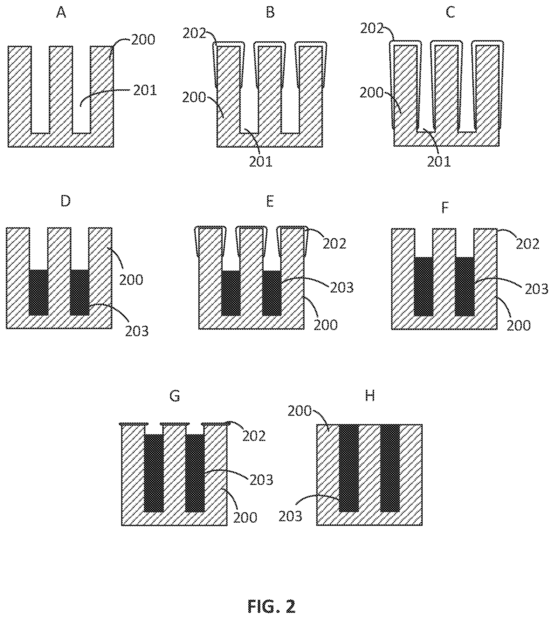
[0088] FIG. 2 is a schematic presentation of an embodiment of a gap being filled according to the current disclosure. Panel A depicts a substrate 200 comprising two gaps 201. In panel B, an inhibition layer 202 has been deposited on the substrate. The inhibition layer 202 is deposited on the top of the substrate and it extends into the gap 201 along the surface of the substrate 200. Panel C depicts a similar situation as Panel B, except that the inhibition layer 202 extends deeper into the gap 201. This situation may have been achieved, for example, by applying higher RF power during supplying the first plasma. The thickness of the inhibition layer 202 in the embodiments of panels B and C may be different, but this is not illustrated in the figure.
[0089] Panels D to H are schematic illustrations of the method according to the current disclosure after a silicon-containing material 203 has been deposited in the gap 201 in one or more deposition cycles. In panels D to H, the gap 201 has been at least partially filled with silicon-containing material 203. Therefore, the reference for gap 201 has been omitted for clarity. Panel D shows the substrate 200 after a deposition of silicon-containing material 203. The inhibition layer 202 has been removed from the substrate 200 during the deposition of the silicon-containing material 203. For example, if the second precursor comprises plasma, such as oxygen plasma, the carbon-containing inhibition layer 202 may be removed from the substrate 200. Although not depicted in FIG. 2, depending on the process conditions, there may be some inhibition layer 202 remaining on the substrate 200.
[0090] Panel E depicts the embodiment of panel D after a further inhibition layer 202 deposition. The process conditions may be varied so that in such a further cycle, the inhibition layer 202 extends less into the gap 201. Panel F and G present similar situations as panes D and E, respectively, after still further cycles of deposition. The number of cycles needed for filling a gap 201 depends on the application in question and may vary from 1 to several hundreds.
[0091] Panel H illustrates the substrate 200 after the gap 201 has been completely filled with the silicon-containing material 203. Although not drawn into the figure, the silicon-containing material 203 may at least partially also cover the top surface of the substrate 200.
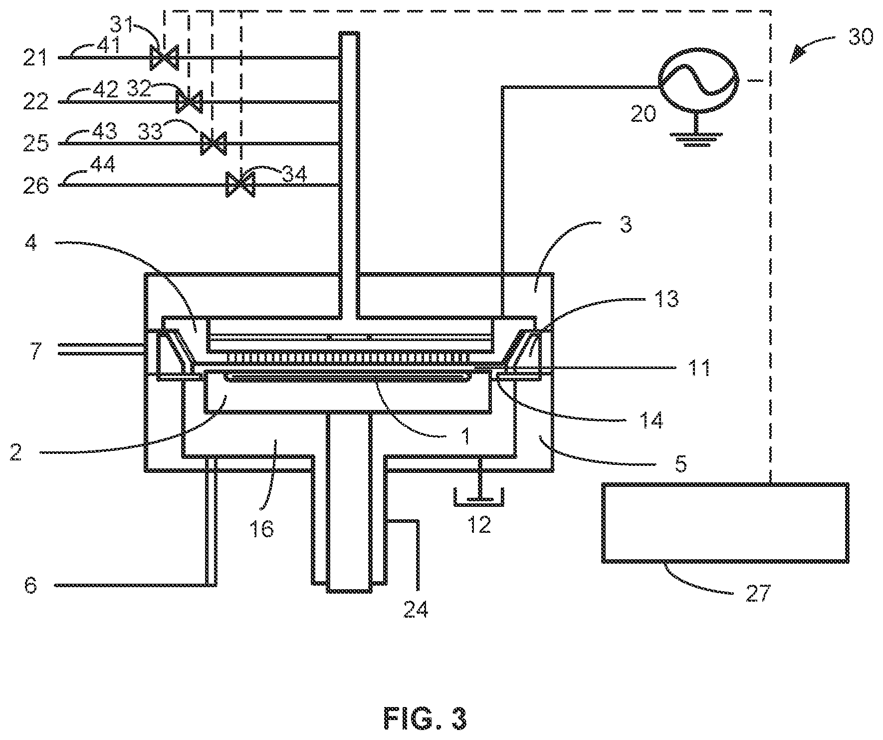
[0092] FIG. 3 illustrates a semiconductor processing apparatus 30 in accordance with exemplary embodiments of the current disclosure. Semiconductor processing apparatus 30 includes one or more reaction chambers 3 for accommodating a substrate 1 comprising a gap. The apparatus comprises a first source 21 for a carbon precursor in gas communication via a first valve 31 with a reaction chamber 3, a second source 22 for a plasma reactant in gas communication via a second valve 32 with a reaction chamber, a third source 25 for a first precursor in gas communication via a third valve 33 with a reaction chamber, and a fourth source 26 for the second precursor in gas communication via a fourth valve 34 with a reaction chamber. The apparatus further comprises a controller 27 operably connected to the first, second, third, and fourth valves 31, 32, 33, 34. The controller 27 is configured and programmed to control supplying a carbon precursor in the reaction chamber 3, supplying first plasma in the reaction chamber 3 to form a first reactive species; and depositing silicon-containing material on the substrate 1.
[0093] In accordance with exemplary aspects, the controller 27 is configured such that the supply times for the carbon precursor, plasma precursor, first precursor and second precursor may be independently selected. An apparatus can include one or more controller(s), such as controller 27, programmed or otherwise configured to cause the deposition processes described herein to be conducted. The controller(s) can be communicated with the various power sources, heating systems, pumps, robotics, and gas flow controllers or valves of the reactor.
[0094] Although not illustrated, semiconductor processing apparatus 30 can include additional sources and additional components, such as those typically found on semiconductor processing apparatus.
[0095] Optionally, semiconductor processing apparatus 30 is provided with a heater to activate the reactions by elevating the temperature of one or more of the substrate, carbon precursor, plasma precursor, first precursor, second precursor, purging gas, inert gas and carrier gas.
[0096] Semiconductor processing apparatus 30 may be provided with a RF power source 20 operably connected with the controller constructed and arranged to produce a plasma of the plasma precursor and/or second precursor.
[0097] The process cycle with a plasma may be performed using semiconductor processing apparatus 30, desirably in conjunction with controls programmed to conduct the sequences described herein, usable in at least some embodiments of the present disclosure. In the apparatus illustrated in FIG. 3, by providing a pair of electrically conductive flat-plate electrodes 4, 2 in parallel and facing each other in the interior 11 (reaction zone) of reaction chamber 3, applying RF power (e.g., 13.56 MHz or 27 MHz) from a power source 20 to one side, and electrically grounding the other side 12, a plasma is excited between the electrodes 4, 2.
[0098] A temperature regulator can be provided in a lower stage 2 (the lower electrode), and a temperature of substrate 1 placed thereon can be kept at a relatively constant temperature. The upper electrode 4 can serve as a shower plate as well, and precursor gases and optionally an inert gas(es) and/or purging gases can be introduced into the reaction chamber 3 through gas lines 41-44, respectively, and through the shower plate 4.
[0099] Additionally, in the reaction chamber 3, a circular duct 13 with an exhaust line 7 is provided, through which gas in the interior 11 of the reaction chamber 3 is exhausted. Additionally, a transfer chamber 5--e.g., disposed below the reaction chamber 3--is provided with a seal gas line 24 to introduce seal gas into the interior 11 of the reaction chamber 3 via the interior 16 (transfer zone) of the transfer chamber 5, wherein a separation plate 14 for separating the reaction zone and the transfer zone is provided (a gate valve through which a wafer is transferred into or from the transfer chamber 5 is omitted from this figure). The transfer chamber is also provided with an exhaust line 6. In some embodiments, the deposition of a carbon-containing inhibition layer and silicon-containing material, and other optional deposition and/or a surface treatment processes are performed in the same reaction space, so that all the steps can continuously be conducted without exposing the substrate 1 to air or other oxygen-containing atmosphere. In some embodiments, a remote plasma unit can be used for exciting a gas--e.g., from one or more of sources 21, 22, 25, and/or 26.
[0100] A first plasma and/or second plasma may be generated in situ, for example, in a gas that flows continuously throughout the deposition process or throughout one deposition cycle. In other embodiments, the plasma may be generated remotely and provided to the reaction chamber.
[0101] In some embodiments, a dual chamber reactor (two sections or compartments for processing wafers disposed closely to each other) can be used, wherein a process gas and an inert gas can be supplied through a shared line, whereas a precursor gas can be supplied through unshared lines.
[0102] It is to be understood that the configurations and/or approaches described herein are exemplary in nature, and that these specific embodiments or examples are not to be considered in a limiting sense, because numerous variations are possible. The specific routines or methods described herein may represent one or more of any number of processing strategies. Thus, the various acts illustrated may be performed in the sequence illustrated, in other sequences, or omitted in some cases.
* * * * *
D00000
D00001
D00002
D00003
P00999
XML
uspto.report is an independent third-party trademark research tool that is not affiliated, endorsed, or sponsored by the United States Patent and Trademark Office (USPTO) or any other governmental organization. The information provided by uspto.report is based on publicly available data at the time of writing and is intended for informational purposes only.
While we strive to provide accurate and up-to-date information, we do not guarantee the accuracy, completeness, reliability, or suitability of the information displayed on this site. The use of this site is at your own risk. Any reliance you place on such information is therefore strictly at your own risk.
All official trademark data, including owner information, should be verified by visiting the official USPTO website at www.uspto.gov. This site is not intended to replace professional legal advice and should not be used as a substitute for consulting with a legal professional who is knowledgeable about trademark law.