Method And Apparatus For Filling A Recess Formed Within A Substrate Surface
Pore; Viljami ; et al.
U.S. patent application number 17/544982 was filed with the patent office on 2022-03-31 for method and apparatus for filling a recess formed within a substrate surface. The applicant listed for this patent is ASM IP Holding B.V.. Invention is credited to Zecheng Liu, Viljami Pore.
| Application Number | 20220102195 17/544982 |
| Document ID | / |
| Family ID | 1000006013237 |
| Filed Date | 2022-03-31 |


| United States Patent Application | 20220102195 |
| Kind Code | A1 |
| Pore; Viljami ; et al. | March 31, 2022 |
METHOD AND APPARATUS FOR FILLING A RECESS FORMED WITHIN A SUBSTRATE SURFACE
Abstract
There is provided a method of filling one or more recesses by providing the substrate in a reaction chamber and introducing a first reactant to the substrate with a first dose, introducing a second reactant to the substrate with a second dose, wherein the first and the second doses overlap in an overlap area where the first and second reactants react and leave an initially substantially unreacted area where the first and the second areas do not overlap; introducing a third reactant to the substrate with a third dose, the third reactant reacting with the first or second reactant to form deposited material; and etching the deposited material. An apparatus for filling a recess is also disclosed.
| Inventors: | Pore; Viljami; (Helsinki, FI) ; Liu; Zecheng; (Helsinki, FI) | ||||||||||
| Applicant: |
|
||||||||||
|---|---|---|---|---|---|---|---|---|---|---|---|
| Family ID: | 1000006013237 | ||||||||||
| Appl. No.: | 17/544982 | ||||||||||
| Filed: | December 8, 2021 |
Related U.S. Patent Documents
| Application Number | Filing Date | Patent Number | ||
|---|---|---|---|---|
| 16792571 | Feb 17, 2020 | 11227789 | ||
| 17544982 | ||||
| 62808251 | Feb 20, 2019 | |||
| Current U.S. Class: | 1/1 |
| Current CPC Class: | H01J 37/32357 20130101; H01J 2237/3341 20130101; H01L 29/0649 20130101; H01L 21/76224 20130101; H01J 37/32449 20130101; H01L 21/67069 20130101 |
| International Class: | H01L 21/762 20060101 H01L021/762; H01L 21/67 20060101 H01L021/67; H01J 37/32 20060101 H01J037/32; H01L 29/06 20060101 H01L029/06 |
Claims
1. A semiconductor processing apparatus comprising: one or more reaction chambers for accommodating a substrate comprising a surface having a recess formed therein; a first source for a first reactant in gas communication via a first valve with one of the reaction chambers; a second source for a second reactant in gas communication via a second valve with one of the reaction chambers; a third source for a third reactant in gas communication via a third valve with one of the reaction chambers; an etchant source in gas communication via a fourth valve with one of the reaction chambers; and a controller operably connected to the first, second, third, and fourth gas valves and configured and programmed to control: introducing the first reactant to the substrate with a first dose on the recess; introducing a second reactant to the substrate with a second dose on the recess, wherein the first and the second doses overlap in an overlap area and leave an area where the first and the second areas do not overlap; introducing a third reactant to the substrate with a third dose, the third reactant reacting with the first or second reactant in the area where the first and the second areas do not overlap, thereby depositing material; and etching the deposited material in the recess.
2. The semiconductor processing apparatus of claim 1, wherein the etchant comprises one or more of C.sub.xF.sub.y, CHF.sub.3, NF.sub.3, SF.sub.6, Cl.sub.2, BCl.sub.3, HBr, and HI.
3. The semiconductor processing apparatus of claim 1, further comprising a remote plasma between the etchant source and the one or more reaction chambers.
Description
CROSS-REFERENCE TO RELATED APPLICATIONS
[0001] This application is a divisional of and claims priority to U.S. patent application Ser. No. 16/792,571 filed Feb. 17, 2020 titled METHOD AND APPARATUS FOR FILLING A RECESS FORMED WITHIN A SUBSTRATE SURFACE; which claims the benefit of U.S. Provisional Patent Application Ser. No. 62/808,251, filed on Feb. 20, 2019, titled METHOD AND APPARATUS FOR FILLING A RECESS FORMED WITHIN A SUBSTRATE SURFACE, the disclosures of which are hereby incorporated by reference in their entirety.
FIELD OF DISCLOSURE
[0002] The present invention generally relates to methods and apparatus for manufacturing electronic devices. More particularly, the invention relates to methods and apparatus for filling one or more recesses formed within a surface of a substrate during the manufacturing of electronic devices.
BACKGROUND
[0003] During manufacturing of electronic devices, such as an integrated circuit (IC), recesses, such as gaps or trenches, can be created within the substrate. Filling the recesses can take a variety of forms, depending upon the specific application.
[0004] A typical trench filling process may be subjected to drawbacks, including void formation in the trench. Voids may be formed when the filling material forms a constriction near the top of the trench before the trench is completely filled. Such voids may compromise device isolation of the devices on the integrated circuit as well as the overall structural integrity of the IC. Unfortunately, preventing void formation during trench fill may often place size constraints on the trenches, which may limit device packing density of the devices.
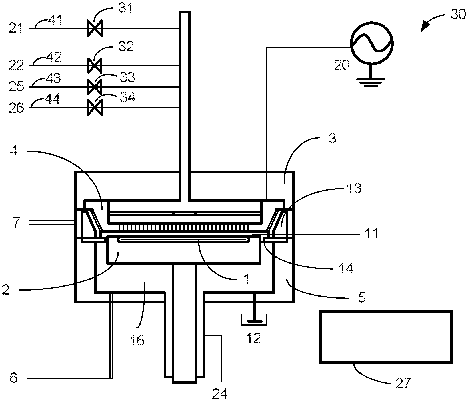
[0005] If the trenches are filled for device isolation, a key parameter in measuring the effectiveness of device isolation may be the field threshold voltage, that is, the voltage necessary to create a parasitic current linking adjacent isolated devices. The field threshold voltage may be influenced by a number of physical and material properties, such as trench width, dielectric constant of the trench filling material, substrate doping, field implant dose and substrate bias during processing.
[0006] Void formation may be mitigated by decreasing trench depth and/or tapering trench sidewalls so that the openings of the trench are wider at the top than at the bottom of the trench. A trade off in decreasing the trench depth may be reducing the effectiveness of the device isolation, while the larger top openings of trenches with tapering sidewalls may use up additional integrated circuit real estate. Such problems can become increasingly problematic when attempting to reduce device dimensions. Accordingly, improved methods and apparatus for filling a recess may be desired.
SUMMARY
[0007] Various embodiments of the present disclosure relate to methods of filling a recess, such as a trench, within a surface of a substrate. While the ways in which various embodiments of the present disclosure address drawbacks of prior methods are discussed in more detail below, in general, various embodiments of the disclosure provide improved methods and apparatus suitable for filling recesses within a substrate surface. For example, exemplary methods and apparatus can be used to seamlessly fill high aspect ratio recesses with desired material, such as dielectric material.
[0008] In accordance with at least one embodiment of the disclosure, a method of filling a recess formed within a substrate surface includes the steps of: providing the substrate in a reaction chamber, introducing a first reactant to the substrate with a first dose on the surface of the recess, introducing a second reactant to the substrate with a second dose on the surface of the recess, wherein the first and the second doses overlap in an overlap area and leave an area where the first and the second doses do not overlap, introducing a third reactant to the substrate with a third dose, the third reactant reacting with the first or second reactant in the area where the first and the second doses do not overlap, thereby depositing material, and etching the deposited material within the recess. In accordance with various aspects, a concentration of the first reactant in the overlap area differs from a concentration of the first reactant in the area where the first and the second areas do not overlap. A number of deposition cycles including the steps of introducing a first reactant to the substrate, introducing a second reactant to the substrate, and introducing a third reactant to the substrate can be repeated one or more times prior to the method proceeding to the step of etching the deposited material. Further, one or more deposition cycles in combination with the step of etching the deposited material can be repeated a number of times to fill the recess. In accordance with further aspects, one of the first and second reactants is introduced with a saturating dose and the other one of the first and second reactants is introduced with a subsaturating dose. In accordance with yet further examples, during the step of etching the deposited material, an etch rate of the material can be higher in the overlap area relative to the area where the first and the second areas do not overlap. By having the doses of the first and second reactants, such that the reactants overlap in an overlap area in the top of the recess, the first and second reactants can react in the top of the recess to block or mitigate further reactions in the top of the recess. In an initially unreacted area in the bottom of the recess where the first and the second reactant did not overlap, the first or second reactant may still react with the third reactant, thereby filling the recess from the bottom upwards.
[0009] According to a further embodiment, there is provided a semiconductor processing apparatus, for example, to provide an improved or at least an alternative recess filling method, such as a method described herein. In accordance with at least one embodiment of the disclosure, a semiconductor processing apparatus includes one or more reaction chambers for accommodating a substrate comprising a surface having a recess formed therein; a first source for a first reactant in gas communication via a first valve with one of the reaction chambers; a second source for a second reactant in gas communication via a second valve with one of the reaction chambers; a third source for a third reactant in gas communication via a third valve with one of the reaction chambers; an etchant source in gas communication via a fourth valve with one of the reaction chambers; and a controller operably connected to the first, second, third, and fourth gas valves and configured and programmed to control: introducing the first reactant to the substrate with a first dose on the recess; introducing a second reactant to the substrate with a second dose on the recess, wherein the first and the second doses overlap in an overlap area and leave an area where the first and the second areas do not overlap (e.g., where a concentration of one of the first and second doses is negligible or less than about one percent of the other of the first or second reactant and/or less than about one percent of the concentration the same reactant in the overlap area); introducing a third reactant to the substrate with a third dose, the third reactant reacting with the first or second reactant in the area where the first and the second areas do not overlap, thereby depositing material; and etching the deposited material in the recess. A deposition cycle including introducing the first reactant, introducing a second reactant, and introducing a third reactant can be repeated as noted above prior to the step of etching the deposited material. Similarly, one or more deposition cycles in combination with the step of etching the deposited material can be repeated a number of times to fill the recess.
[0010] In accordance with yet further exemplary embodiments of the disclosure, a semiconductor structure can be formed using a method and/or an apparatus as described herein.
[0011] For purposes of summarizing the invention and the advantages achieved over the prior art, certain objects and advantages of the invention have been described herein above. Of course, it is to be understood that not necessarily all such objects or advantages may be achieved in accordance with any particular embodiment of the invention. Thus, for example, those skilled in the art will recognize that the invention may be embodied or carried out in a manner that achieves or optimizes one advantage or group of advantages as taught or suggested herein without necessarily achieving other objects or advantages as may be taught or suggested herein. These and other embodiments will become readily apparent to those skilled in the art from the following detailed description of certain embodiments having reference to the figures, the invention not being limited to any particular embodiment(s) disclosed.
BRIEF DESCRIPTION OF THE DRAWING FIGURES
[0012] A more complete understanding of exemplary embodiments of the present disclosure can be derived by referring to the detailed description and claims when considered in connection with the following illustrative figures.
[0013] FIG. 1A illustrates a schematic representation of a PEALD (plasma-enhanced atomic layer deposition) apparatus suitable for filling a recess in accordance with at least one embodiment of the present disclosure.
[0014] FIG. 1B illustrates a schematic representation of a precursor supply system using a flow-pass system (FPS) usable in accordance with at least one embodiment of the present disclosure.
[0015] FIG. 2 illustrates a flowchart of a method for filling a recess in accordance with at least one embodiment of the disclosure.
[0016] FIG. 3 illustrates a flowchart of a method for filling a recess in accordance with another embodiment of the disclosure.
[0017] FIG. 4 illustrates a structure in accordance with another embodiment of the disclosure.
DETAILED DESCRIPTION OF EXEMPLARY EMBODIMENTS
[0018] Although certain embodiments and examples are disclosed below, it will be understood by those in the art that the invention extends beyond the specifically disclosed embodiments and/or uses of the invention and obvious modifications and equivalents thereof. Thus, it is intended that the scope of the invention disclosed should not be limited by the particular disclosed embodiments described below.
[0019] Turning now to the figures, FIG. 2 illustrates a flowchart of a method 100 in accordance with at least one embodiment of the disclosure. Method 100 can be used to, for example, fill one or more recesses, sometimes referred to as gaps or features, created during manufacturing of a structure. The recesses may be less than 40 or even 20 nm wide and/or may be more than 40, 100, 200 or even 400 nm deep. An aspect ratio of the recesses can range from, for example, about 5:1 to about 30:1.
[0020] As illustrated in FIG. 2, method 100 includes the steps of providing the substrate in a reaction chamber (step 105), introducing a first reactant to the substrate with a first dose on the surface of the recess (step 110), introducing a second reactant to the substrate with a second dose on the surface of the recess (step 120), introducing a third reactant to the substrate with a third dose, the third reactant reacting with the first or second reactant in the area where the first and the second dose do not overlap, thereby depositing material (step 130), and etching the deposited material in the recess (step 140).
[0021] Step 105 includes providing a substrate to a reaction chamber. As used herein, a "substrate" refers to any material having a surface onto which material can be deposited. A substrate may include a bulk material such as silicon (e.g., single crystal silicon) or may include one or more layers overlying the bulk material. Further, the substrate may include various topologies, such as recesses (e.g., trenches or vias), lines, and the like formed within or on at least a portion of a layer of the substrate. By way of particular example, a substrate can include layers of SiN, SiOx and/or W, at least one of these layers having at least one recess formed therein.
[0022] During step 105, the substrate may be brought to a desired temperature using, for example, a substrate heater and/or radiative or other heaters. A temperature during steps 110-130 or 110-140 can range from about 100.degree. C. to about 550.degree. C. or about 250.degree. C. to about 450.degree. C. A pressure within the reaction chamber during such steps can be from about 1 to about 9 or about 3 to about 7 Torr.
[0023] In accordance with various examples of the disclosure, by having the doses of the first and second reactants, such that the reactants overlap in the top of the recess, the first and second reactants can react in the top (overlap area), blocking or substantially blocking further reactions in the top of the recess. In the bottom of the recess, where the first and the second reactants did not overlap (e.g., where a concentration of one of the reactants is significantly lower--e.g., less than about one percent of the other and/or less than about one percent of the concentration in the overlap area), the reactant can still react with the third reactant to thereby deposit material.
[0024] In accordance with examples of the disclosure, the dose of one of the first and the second reactants is saturating (e.g., relatively high amount or concentration and/or long pulse time), so that said one of the first and second reactants covers the whole or substantially the whole recess, while the dose of the other one of the first and second reactants is subsaturating (e.g., relatively short pulse time and/or low concentration/amount) to facilitate the first and second reactants only or substantially only overlapping in the top (overlap) area of the recess. In this context, relatively low can mean about ten, five, two, or one percent or less of a concentration and/or pulse amount or time of one reactant compared to another reactant, and relatively high can mean the other reactant has a concentration and/or pulse amount or time that is about 10, 20, 50, or about 100 times greater for one reactant than the other.
[0025] A deposition cycle can include steps 110-130. The deposition cycle can be repeated multiple times to fill the recess as depicted by the loop 150. The deposition cycle may be repeated, for example, between about 1 to 10,000 times, about 5 to 2,000 times or between about 10 and 1,000 times. Any excess reactant and/or byproduct can be removed after one or more (e.g., each) of steps 110-130 and/or 140 to circumvent direct reactions between the reactants that might otherwise cause contamination within the reaction chamber.
[0026] Method 100 may also be repeated partly via loop 160 if, for example, the top of the recess is still blocking the reactants for reaction in the bottom area. Also, combinations of a complete repeat via loop 150 and a partial repeat via loop 160 may be made. In this way, the speed of the recess fill method may be increased.
[0027] As noted above, one of the first and the second reactants can be introduced with a saturating (e.g., relatively large or long dose) and the other one of the first and second reactants can be introduced with a subsaturating (e.g., relatively low or short dose). The reactant that is provided with the saturating dose can penetrate deep in the recess to reach the bottom of the recess, whereas the reactant that is provided with the subsaturating dose will not penetrate deep in the recess and stay in the area. The reaction between the first and second reactant may therefore only or substantially only occur in the top/overlap area of the recess, thereby blocking or substantially blocking further reaction in the top/overlap area.
[0028] One of the first and the second reactants may be a potential growth reactant, whereas the other one of the first and second reactants may comprise a low growth reactant, providing a relatively low growth in combination with the potential growth reactant. The reaction between the first and second reactants may therefore result in a relatively low growth in the top/overlap area of the recess, such that the top/overlap area may not be blocked by depositing material before the bottom of the recess is substantially filled.
[0029] One of the first and the second reactants may be introduced to cover said corresponding one of the first and second areas, which substantially covers the total surface of the one or more recesses. The one of the first and second reactants may be the potential growth reactant providing potential growth dependent on the other reactant.
[0030] The one of the first and second reactants which is the potential growth reactant may comprise silicon. The first/second/potential growth reactant can be selected from the group consisting of silane amines, siloxane amines, silazane amines, (amino silanes, amino siloxanes, and amino silazanes). For example, the potential growth reactant may comprise silanediamine such as N,N,N',N'-tetraethyl silanediamine, such as sold by Air Liquide (Paris, France) under the name ALOHA.TM. SAM.24.
[0031] The substantial low growth reactant may comprise one or more of He, Ne, Ar, Kr, Xe, N.sub.2, NH.sub.3 and N.sub.2H.sub.4, which may optionally be activated by a (direct or remote) plasma. Nitrogen in combination with a potential growth reactant can result in a relatively low growth in the top of the recess. In some cases, it may be advantageous to provide the substantial low growth reactant before providing the potential growth reactant.
[0032] The third reactant may comprise a high growth reactant providing a relatively high growth in combination with the potential growth reactant. The third reactant may be introduced with a relatively large dose to ensure that the bottom of the recess is reached by the third reactant so that the third reactant may react with the potential growth reactant in the bottom of the recess. Reaction in the top of the trench for the third reactant can be blocked because the first and the second reactants may already have been reacted in the top of the recess.
[0033] The third reactant may comprise an oxidant, such as one or more reactants selected from the group consisting of water, hydrogen peroxide, molecular oxygen and ozone, which may be activated by a (direct or remote) plasma. Oxygen in combination with a silane amine (e.g., silanediamine, such as N,N,N',N'-tetraethyl silanediamine) may result in a relatively high growth in the bottom of the recess. For example, one may provide N,N,N',N'-tetraethyl silanediamine, N plasma, and then O plasma in a cyclic repetitive reaction to deposit material. Alternatively, one may provide N plasma, N,N,N',N'-tetraethyl silanediamine, and then O plasma in a cyclic repetitive reaction to deposit the material.
[0034] As illustrated in FIG. 2, after at least one deposition cycle (steps 110-130), the step of etching deposited material 140 is performed. Step 140 can be configured, such that an etch rate of deposited material is higher in a top (e.g., overlap) area of the recess, relative to a bottom area (e.g., area where the doses to not overlap) of the recess. A number of repetitions of loops 150, 160, relative to a loop 170 can be manipulated based on, for example, the dimensions (e.g., height, width, or aspect ratio), configurations (e.g., how close together the recesses are), and/or geometry (e.g., the shape of the recess opening and/or shape of the walls of the recess) of the recesses.
[0035] In accordance with various examples of the disclosure, step 140 includes a dry etch process. An etchant used during step 140 can be activated by, for example, a direct or remote plasma unit. Exemplary etchants that can be used include a halogen; specific examples include C.sub.xF.sub.y, where x and y are integers (e.g., CF.sub.4, C.sub.2F.sub.6, C.sub.3F.sub.8, or C.sub.4F.sub.8), CHF.sub.3, NF.sub.3, SF.sub.6, Cl.sub.2, BCl.sub.3, HBr, and HI. Additive gasses, such as N.sub.2, O.sub.2, Ar, He, NO, and the like can additionally be used to control the etching of deposited material during step 140. By way of particular example, step 140 can be performed at a substrate temperature of about 25.degree. C. to about 550.degree. C. or about 100.degree. C. to about 300.degree. C. The pressure within the reaction chamber can be about 0.05 Torr to about 5 Torr or about 0.2 Torr to about 3 Torr. And a flowrate of an etchant and/or additive can be from about 30 sccm to about 3000 sccm or about 100 sccm to about 1000 sccm.
[0036] FIG. 3 illustrates a flowchart of a method 200 in accordance with at least one embodiment of the disclosure. Method 200 is similar to method 100, except method 200 includes a step 230 of introducing one of the first and second reactants again to the substrate before the third reactant. Steps 205, 210, 220, 240, and 250 can be the same or similar to steps 105-140 described above in connection with FIG. 2. Further, method 200 can include loops 260, 270 to repeat portions or all of method 200.
[0037] For example, one may provide a silicon reactant, such as N,N,N',N'-tetraethyl silanediamine, a nitrogen reactant, e.g., comprising nitrogen plasma, and an oxygen reactant, e.g., comprising an oxygen plasma and then nitrogen plasma one or more times before proceeding to the step of etching deposited material (step 250). Loop 260 and/or loop 270 may be repeated, for example, about 1 to 10,000 times, 5 to 2,000 times or between 10 and 1,000 times. By adding step 230 (e.g., doubling the nitrogen plasma steps) in the sequence, it is better assured that the reactants in the top have reacted and are substantially deactivated before the third reactant (e.g., oxygen) plasma is provided.
[0038] The third reactant may comprise an oxidant--e.g., ozone and/or hydrogen peroxide which in combination with silanediamine such as N,N,N',N'-tetraethyl silanediamine may result in high growth. Ozone, and/or hydrogen peroxide do not need to be activated by a plasma to react with the silanediamine to provide for relatively high growth and that is beneficial because the energy of the plasma may be lower deep in the recess.
[0039] The reactants for steps 210-250 can be the same or similar to those described above. Alternatively, the potential growth reactant may comprise an organometal, e.g., an organoaluminium such as trimethylaluminium (TMA). If the potential growth reactant comprises an organometal, e.g., an organoaluminium such as trimethylaluminium (TMA), the substantial low growth reactant may comprise ozone. Ozone in combination with trimethylaluminium may result in low growth in the top of the recess.
[0040] The third reactant may comprise hydrogen peroxide, which in combination with trimethylaluminium, may result in high growth in the bottom of the recess; hydrazine, which in combination with trimethylaluminium, may result in high growth in the bottom of the recess; and/or water, which in combination with trimethylaluminium, may result in high growth in the bottom of the recess.
[0041] FIG. 4 illustrates a structure 400 formed in accordance with exemplary methods (e.g., method 100 or method 200) and/or using an apparatus as described herein. Structure 400 includes a substrate 402, a recess 404 formed therein, and deposited material 406. Deposited material 406 can be seamless, such that no visible void in deposited material 406 is formed.
[0042] Turning now to FIG. 1A and FIG. 1B, a semiconductor processing apparatus 30 is illustrated. Semiconductor processing apparatus 30 includes one or more reaction chambers 3 for accommodating a substrate comprising a surface having a recess formed therein; a first source 21 for a first reactant in gas communication via a first valve 31 with one of the reaction chambers; a second source 22 for a second reactant in gas communication via a second valve 32 with one of the reaction chambers; a third source 25 for a third reactant in gas communication via a third valve 33 with one of the reaction chambers; an etchant or fourth source 26 in gas communication via a fourth valve 34 with one of the reaction chambers; and a controller 27 operably connected to the first, second, third, and fourth gas valves and configured and programmed to control: introducing the first reactant to the substrate with a first dose on the recess; introducing a second reactant to the substrate with a second dose on the recess, wherein the first and the second dose overlap in an overlap area and leave an area where the first and the second areas do not overlap; introducing a third reactant to the substrate with a third dose, the third reactant reacting with the first or second reactant in the area where the first and the second areas do not overlap, thereby depositing material; and etching the deposited material in the recess. Although not illustrated, semiconductor processing apparatus 30 can include additional sources (e.g., for additives as described herein, for inert gasses, and the like) and additional components.
[0043] Optionally, semiconductor processing apparatus 30 is provided with a heater to activate the reactions by elevating the temperature of one or more of the substrate, the first, second and third reactants, the etchant and/or additives. Exemplary single wafer reactors, designed specifically to perform ALD processes, are commercially available from ASM International NV (Almere, The Netherlands) under the tradenames Pulsar.RTM., Emerald.RTM., Dragon.RTM. and Eagle.RTM.. Exemplary batch ALD reactors, designed specifically to perform ALD processes, are also commercially available from ASM International NV under the tradenames A400.TM. and A412.TM..
[0044] Optionally, the semiconductor processing apparatus 30 may be provided with a radiofrequency source operably connected with the controller constructed and arranged to produce a plasma of the first, second or third reactant and/or etchant and/or additive. The plasma enhanced atomic layer deposition (PEALD) may be performed in an Eagle.RTM. XP8 PEALD reactor available from ASM International NV of Almere, the Netherlands which apparatus comprises a plasma source to activate one or more of the reactants.
[0045] The process cycle with a plasma may be performed using semiconductor processing apparatus 30, desirably in conjunction with controls programmed to conduct the sequences described herein, usable in at least some embodiments of the present disclosure. In the apparatus illustrated in FIG. 1A, by providing a pair of electrically conductive flat-plate electrodes 4, 2 in parallel and facing each other in the interior 11 (reaction zone) of reaction chamber 3, applying RF power (e.g., 13.56 MHz or 27 MHz) from a power source 20 to one side, and electrically grounding the other side 12, a plasma is excited between the electrodes.
[0046] A temperature regulator is provided in a lower stage 2 (the lower electrode), and a temperature of substrate 1 placed thereon can be kept at a relatively constant temperature. The upper electrode 4 serves as a shower plate as well, and reactant gas (and optionally a noble gas), precursor gasses, and etchant gas are introduced into the reaction chamber 3 through gas lines 41-44, respectively, and through the shower plate 4.
[0047] Additionally, in the reaction chamber 3, a circular duct 13 with an exhaust line 7 is provided, through which gas in the interior 11 of the reaction chamber 3 is exhausted. Additionally, a transfer chamber 5--e.g., disposed below the reaction chamber 3, is provided with a seal gas line 24 to introduce seal gas into the interior 11 of the reaction chamber 3 via the interior 16 (transfer zone) of the transfer chamber 5, wherein a separation plate 14 for separating the reaction zone and the transfer zone is provided (a gate valve through which a substrate is transferred into or from the transfer chamber 5 is omitted from this figure). The transfer chamber is also provided with an exhaust line 6. In some embodiments, the deposition of multi-element film and surface treatment are performed in the same reaction space, so that all the steps can continuously be conducted without exposing the substrate to air or other oxygen-containing atmosphere. In some embodiments, a remote plasma unit can be used for exciting a gas--e.g., from one or more of sources 21, 22, 25, and/or 26.
[0048] In some embodiments, in the apparatus depicted in FIG. 1A, a system of switching flow of an inactive gas and flow of a precursor or reactant gas is illustrated in FIG. 1B; this system can be used to introduce the precursor or reactant gas in pulses without substantially fluctuating pressure of the reaction chamber. FIG. 1B illustrates a precursor supply system using a flow-pass system (FPS) according to an embodiment of the present invention (black valves indicate that the valves are closed). As shown in (a) in FIG. 1B, when feeding a precursor to a reaction chamber (not shown), first, a carrier gas such as Ar (or He) flows through a gas line with valves b and c, and then enters a bottle (reservoir) 20. The carrier gas flows out from the bottle 20 while carrying a precursor gas in an amount corresponding to a vapor pressure inside the bottle 20 and flows through a gas line with valves f and e, and is then fed to the reaction chamber together with the precursor. In this case, valves a and d are closed. When feeding only the carrier gas (e.g., a noble gas) to the reaction chamber, as shown in (b) in FIG. 1B, the carrier gas flows through the gas line with the valve while bypassing the bottle 20. In this case, valves b, c, d, e, and f are closed.
[0049] The precursor may be provided with the aid of a carrier gas. In the case of ALD, which is a self-limiting adsorption reaction process, a number of deposited precursor molecules can be determined by the number of reactive surface sites and is independent of precursor exposure after saturation, and a supply of the precursor is such that the reactive surface sites are saturated thereby per cycle. A plasma for deposition may be generated in situ, for example, in a gas that flows continuously throughout the deposition cycle. In other embodiments, the plasma may be generated remotely and provided to the reaction chamber.
[0050] In some embodiments, a dual chamber reactor (two sections or compartments for processing substrates disposed closely to each other) can be used, wherein a reactant gas and a noble gas can be supplied through a shared line whereas a precursor gas is supplied through unshared lines.
[0051] A skilled artisan will appreciate that the apparatus includes one or more controller(s), such as controller 27, programmed or otherwise configured to cause the deposition processes described elsewhere herein to be conducted. The controller(s) can be communicated with the various power sources, heating systems, pumps, robotics, and gas flow controllers or valves of the reactor.
[0052] It is to be understood that the configurations and/or approaches described herein are exemplary in nature, and that these specific embodiments or examples are not to be considered in a limiting sense, because numerous variations are possible. The specific routines or methods described herein may represent one or more of any number of processing strategies. Thus, the various acts illustrated may be performed in the sequence illustrated, in other sequences, or omitted in some cases.
[0053] The subject matter of the present disclosure includes all novel and nonobvious combinations and sub-combinations of the various processes, systems, and configurations, and other features, functions, acts, and/or properties disclosed herein, as well as any and all equivalents thereof.
* * * * *
D00000
D00001
D00002
D00003
D00004
XML
uspto.report is an independent third-party trademark research tool that is not affiliated, endorsed, or sponsored by the United States Patent and Trademark Office (USPTO) or any other governmental organization. The information provided by uspto.report is based on publicly available data at the time of writing and is intended for informational purposes only.
While we strive to provide accurate and up-to-date information, we do not guarantee the accuracy, completeness, reliability, or suitability of the information displayed on this site. The use of this site is at your own risk. Any reliance you place on such information is therefore strictly at your own risk.
All official trademark data, including owner information, should be verified by visiting the official USPTO website at www.uspto.gov. This site is not intended to replace professional legal advice and should not be used as a substitute for consulting with a legal professional who is knowledgeable about trademark law.