Method For Providing A Semiconductor Device With Silicon Filled Gaps
Pierreux; Dieter ; et al.
U.S. patent application number 17/093224 was filed with the patent office on 2021-05-20 for method for providing a semiconductor device with silicon filled gaps. The applicant listed for this patent is ASM IP Holding B.V.. Invention is credited to Kelly Houben, Bert Jongbloed, Dieter Pierreux, Anna Trovato, Steven van Aerde, Wilco A. Verweij.
| Application Number | 20210151315 17/093224 |
| Document ID | / |
| Family ID | 1000005247757 |
| Filed Date | 2021-05-20 |

| United States Patent Application | 20210151315 |
| Kind Code | A1 |
| Pierreux; Dieter ; et al. | May 20, 2021 |
METHOD FOR PROVIDING A SEMICONDUCTOR DEVICE WITH SILICON FILLED GAPS
Abstract
Method for filling a gap, comprising providing in a deposition chamber a semiconductor substrate having a gap, wherein a bottom of the gap includes a crystalline semiconducting material and wherein a side wall of the gap includes an amorphous material; depositing a silicon precursor in the gap.
| Inventors: | Pierreux; Dieter; (Dilbeek, BE) ; Trovato; Anna; (Woluwe Saint Pierre, BE) ; Houben; Kelly; (Lubbeek, BE) ; van Aerde; Steven; (Tielt-Winge, BE) ; Jongbloed; Bert; (Oud-Heverlee, BE) ; Verweij; Wilco A.; (Nijkerk, NL) | ||||||||||
| Applicant: |
|
||||||||||
|---|---|---|---|---|---|---|---|---|---|---|---|
| Family ID: | 1000005247757 | ||||||||||
| Appl. No.: | 17/093224 | ||||||||||
| Filed: | November 9, 2020 |
Related U.S. Patent Documents
| Application Number | Filing Date | Patent Number | ||
|---|---|---|---|---|
| 62936071 | Nov 15, 2019 | |||
| Current U.S. Class: | 1/1 |
| Current CPC Class: | H01L 23/53271 20130101; H01L 21/28525 20130101; H01L 23/5226 20130101; H01L 21/0262 20130101; H01L 21/31116 20130101; H01L 21/76879 20130101; H01L 21/02579 20130101; H01L 21/02532 20130101; H01L 21/02576 20130101 |
| International Class: | H01L 21/02 20060101 H01L021/02; H01L 23/522 20060101 H01L023/522; H01L 23/532 20060101 H01L023/532; H01L 21/768 20060101 H01L021/768; H01L 21/311 20060101 H01L021/311; H01L 21/285 20060101 H01L021/285 |
Claims
1. Method for filling a gap, comprising providing in a deposition chamber a semiconductor substrate having a gap, wherein a bottom of the gap includes a crystalline semiconducting material and wherein a side wall of the gap includes an amorphous material; depositing a silicon precursor in the gap to cause an epitaxial growth of the crystalline semiconducting material on the bottom of the gap; providing an etchant in the gap to etch an amorphous deposition of the silicon precursor on the side walls of the gap.
2. Method according to claim 1, wherein the steps of depositing the silicon precursor and providing the etchant are repeated alternatingly.
3. Method according to claim 1, wherein an etch rate of the etchant on the amorphous deposition of the silicon precursor on the side walls of the gap is at least five times higher than an etch rate of the etchant on the crystalline semiconducting material on the bottom of the gap.
4. Method according to claim 1, wherein the crystalline semiconducting material includes silicon, silicon-germanium or germanium.
5. Method according to claim 1, wherein the amorphous material includes silicon oxide and/or silicon nitride.
6. Method according to claim 1, wherein the silicon precursor includes a silane, disilane, or trisilane.
7. Method according to claim 1, wherein the etchant includes dichlorine or hydrogen chloride.
8. Method according to claim 1, wherein providing the etchant in the gap is done by vapour etching.
9. Method according to claim 1, comprising the step of etching a top oxide layer from the crystalline semiconducting material on the bottom of the gap before starting depositing the silicon precursor.
10. Method according to claim 1, wherein the step of providing a silicon precursor in the gap includes depositing a dopant in the gap.
11. Method according to claim 10, wherein the dopant includes phosphine, arsine, or boron trichloride.
12. Method according to claim 1, wherein the depositing of the silicon precursor and the depositing of an etching are done in a temperature range of more or less 350.degree. C.-550.degree. C.
13. Method according to claim 1, wherein the deposition chamber is a process chamber of a batch furnace.
14. A semiconductor device having a gap which is filled according to a method according to claim 1.
15. Semiconductor device according to claim 14, wherein the filled gap is a contact plug, the filled gap providing electrical contact between two layers.
16. Semiconductor device according to claim 15, wherein the device is a memory device.
Description
CROSS-REFERENCE TO RELATED APPLICATIONS
[0001] This application claims priority to U.S. Provisional Patent Application Ser. No. 62/936,071 filed Nov. 15, 2019 titled METHOD FOR PROVIDING A SEMICONDUCTOR DEVICE WITH SILICON FILLED GAPS, the disclosures of which are hereby incorporated by reference in their entirety.
FIELD
[0002] The present disclosure generally relates to methods to manufacture semiconductor devices. More particularly, the disclosure relates to providing amorphous silicon filled gaps.
BACKGROUND
[0003] Semiconductor devices typically include gaps that have been filled with silicon, which may form constituent parts of various electronic devices. The fill may include depositing a layer of silicon on side and bottom surfaces of the gaps, with the layer filling in the gap from the sides and bottom as it grows.
[0004] The growth of the layer may not be completely uniform, however, causing voids, such as seams, to form in the interior of the filled gap. In some cases, these voids may be caused by the deposition process, in which silicon may deposit at a higher rate at the top of the gap than at the bottom, thereby causing the top of the gap to close up first, leaving the voids in the interior of the gap or the nucleation on the bottom or side of the gap may be incomplete causing voids in the bottom or side of the gap.
[0005] Accordingly, there is a need for an improved process for forming silicon filled gaps.
SUMMARY
[0006] In an embodiment, a method for filling a gap is provided. The methods comprises providing in a deposition chamber a semiconductor substrate having a gap, a bottom of the gap including a crystalline semiconducting material and a side wall of the gap including an amorphous material. A silicon precursor is deposited in the gap to cause an epitaxial growth of the crystalline semiconducting material on the bottom of the gap. Then an etchant is provided in the gap to etch an amorphous deposition of the silicon precursor on the side walls of the gap.
[0007] In an embodiment, a semiconductor device is provided. The semiconductor has a gap which is filled according to the method as described above. The silicon filled gap may provide an electrical contact between two layers.
BRIEF DESCRIPTION OF THE DRAWINGS
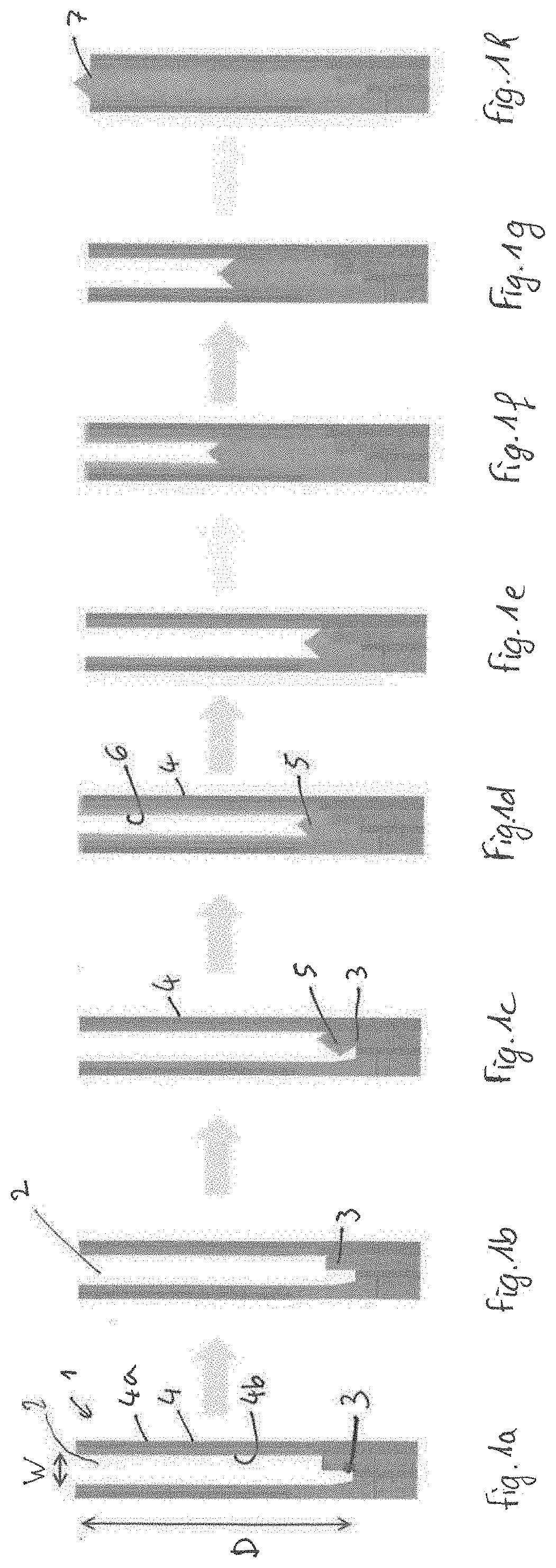
[0008] FIGS. 1a-1h show a schematic series of cross-sections of a gap being filled with silicon according to a preferred embodiment of the method according to the invention.
DETAILED DESCRIPTION
[0009] FIG. 1a shows a schematic cross-section of a substrate 1 having a gap 2. The bottom 3 of the gap 2 includes a crystalline semiconducting material, such as for example crystalline silicon, silicon-germanium or germanium. A depth D of the gap 2 may for example be substantially 200 nm, or more or less, while the gap 2 may have a width W of for example substantially 14 nm or more or less. A side wall 4 of the gap 2 may include an amorphous material. Such an amorphous material may include silicon oxide and/or silicon nitride. In the present embodiment, the side wall 4 may include an external filler layer 4a of for example silicon oxide and an internal spacer layer 4b of for example silicon nitride.
[0010] Since contact of silicon with air may cause an oxide layer to be formed on top of the crystalline semiconducting material, a step of etching a top oxide layer from the crystalline semiconducting material on the bottom 3 of the gap 2 may optionally be performed before starting depositing a silicon precursor, as shown in FIG. 1b. This may for example be done with a known method such as a HF dip etching method.
[0011] Then a silicon precursor, such as for example Silcore.RTM. (Si.sub.3H.sub.8), silane (SiH.sub.4), or disilane (Si.sub.2H.sub.6), may be deposited in the gap 2 to cause an epitaxial growth of the crystalline semiconducting material on the bottom 3 of the gap 2. Optionally, one or more of the hydrogen groups in the silanes may be replaced with one halogen. It has been shown that deposition of the silicon precursor causes a faster nucleation on a crystalline structure than on an amorphous structure. As a consequence, the deposition of the silicon precursor may cause an epitaxial growth 5 of the crystalline semiconducting material on the bottom 3 of the gap, shown in FIG. 1c, while the amorphous material of the side walls temporarily inhibits nucleation on the side wall 4, or in other words, nucleation on the amorphous material on the side wall 4 may be slower than on the bottom of the gap 2.
[0012] Despite a slower nucleation on the side wall 4 of the gap 2 than on the bottom 3 of the gap 2, a silicon film 6 may eventually also form on the side wall 4, as shown in FIG. 1d, which silicon film 6 may be an amorphous silicon film, since it is growing on an amorphous material. After said amorphous silicon film 6 has formed on the side wall 4, and before said amorphous film 6 can close the gap 2, an etching step is performed, in particular a vapour etching step, including providing an etchant, such as for example dichlorine Cl.sub.2 or hydrogen chloride HCl, in the gap 2 to etch an amorphous deposition of the silicon precursor, in particular the amorphous film 6, on the side wall 4 of the gap 2.
[0013] Again, the difference in morphology between the bottom 3 of the gap 2, which includes a crystalline semiconducting material on which epitaxial growth of the silicon deposition has occurred, and the side wall 4 including an amorphous material covered by an amorphous silicon film 6, causes a difference in etch rate, the etch rate of the amorphous silicon film 6 being higher, for example at least five times and preferable even ten times higher or more, than the etch rate of the crystalline epi. As a result, shown in FIG. 1e, it is possible to etch away the silicon film 6 almost without etching the crystalline epi, and without damaging the side wall 4 of the gap 2.
[0014] By repeating the steps of depositing the silicon precursor and providing the etchant in the gap alternatingly, as shown in FIGS. 1f and 1g respectively, one may fill a gap with silicon, in particular with epi-silicon, from the bottom 3 of the gap 2 up towards a top 7 of the gap, or at least until a desired filling height, without creating hardly any void in the filled gap 2.
[0015] In an embodiment, the step of providing a silicon precursor in the gap may also include depositing a dopant in the gap 2, preferably as a co-flow or, alternatively, in an alternating manner. The dopant may for example be a p-doped dopant, and can include phosphine, arsine, or boron trichloride, for example in a concentration of 1E21.
[0016] In an embodiment, the depositing of the silicon precursor and the depositing of an etching may be done in a temperature range of more or less 350.degree. C.-550.degree. C.
[0017] In an embodiment, the gap filled according to the method as described above may be a contact plug, the filled gap providing electrical contact between two layers, for example in a semiconductor device, such as for example a memory device.
[0018] It will be appreciated by those skilled in the art that various omissions, additions and modifications can be made to the processes and structures described above without departing from the scope of the invention. It is contemplated that various combinations or sub-combinations of the specific features and aspects of the embodiments may be made and still fall within the scope of the description. Various features and aspects of the disclosed embodiments can be combined with, or substituted for, one another in order. All such modifications and changes are intended to fall within the scope of the invention, as defined by the appended claims.
* * * * *
D00000
D00001
XML
uspto.report is an independent third-party trademark research tool that is not affiliated, endorsed, or sponsored by the United States Patent and Trademark Office (USPTO) or any other governmental organization. The information provided by uspto.report is based on publicly available data at the time of writing and is intended for informational purposes only.
While we strive to provide accurate and up-to-date information, we do not guarantee the accuracy, completeness, reliability, or suitability of the information displayed on this site. The use of this site is at your own risk. Any reliance you place on such information is therefore strictly at your own risk.
All official trademark data, including owner information, should be verified by visiting the official USPTO website at www.uspto.gov. This site is not intended to replace professional legal advice and should not be used as a substitute for consulting with a legal professional who is knowledgeable about trademark law.