Solder Particles
AKAI; Kunihiko ; et al.
U.S. patent application number 17/255982 was filed with the patent office on 2021-04-22 for solder particles. This patent application is currently assigned to Showa Denko Materials Co., Ltd.. The applicant listed for this patent is Showa Denko Materials Co., Ltd.. Invention is credited to Kunihiko AKAI, Yoshinori EJIRI, Masayuki MIYAJI, Toshimitsu MORIYA, Yuuhei OKADA, Shinichirou SUKATA.
| Application Number | 20210114145 17/255982 |
| Document ID | / |
| Family ID | 1000005332327 |
| Filed Date | 2021-04-22 |


| United States Patent Application | 20210114145 |
| Kind Code | A1 |
| AKAI; Kunihiko ; et al. | April 22, 2021 |
SOLDER PARTICLES
Abstract
The present invention relates to solder particles, each of which partially has a flat portion in the surface. By using these solder particles, electrodes facing each other are able to be appropriately connected, thereby achieving an anisotropic conductive material that exhibits excellent conduction reliability and excellent insulation reliability.
| Inventors: | AKAI; Kunihiko; (Chiyoda-ku, Tokyo, JP) ; EJIRI; Yoshinori; (Chiyoda-ku, Tokyo, JP) ; OKADA; Yuuhei; (Chiyoda-ku, Tokyo, JP) ; MORIYA; Toshimitsu; (Chiyoda-ku, Tokyo, JP) ; SUKATA; Shinichirou; (Chiyoda-ku, Tokyo, JP) ; MIYAJI; Masayuki; (Chiyoda-ku, Tokyo, JP) | ||||||||||
| Applicant: |
|
||||||||||
|---|---|---|---|---|---|---|---|---|---|---|---|
| Assignee: | Showa Denko Materials Co.,
Ltd. Tokyo JP |
||||||||||
| Family ID: | 1000005332327 | ||||||||||
| Appl. No.: | 17/255982 | ||||||||||
| Filed: | June 26, 2019 | ||||||||||
| PCT Filed: | June 26, 2019 | ||||||||||
| PCT NO: | PCT/JP2019/025499 | ||||||||||
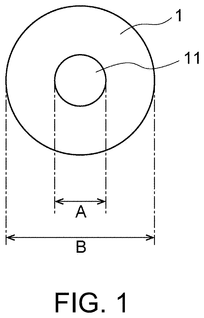
| 371 Date: | December 23, 2020 |
| Current U.S. Class: | 1/1 |
| Current CPC Class: | B23K 35/262 20130101; B23K 2103/08 20180801; B23K 35/0244 20130101 |
| International Class: | B23K 35/02 20060101 B23K035/02; B23K 35/26 20060101 B23K035/26 |
Foreign Application Data
| Date | Code | Application Number |
|---|---|---|
| Jun 26, 2018 | JP | 2018-121088 |
| Jan 30, 2019 | JP | 2019-014853 |
Claims
1. A solder particle having a flat portion on a part of the surface.
2. The solder particle according to claim 1, having an average particle diameter of 1 to 30 .mu.m and a C.V. value of 20% or less.
3. The solder particle according to claim 1, wherein a ratio (A/B) of a diameter A of the flat portion to a diameter B of the solder particle satisfies the following formula: 0.01<A/B<1.0.
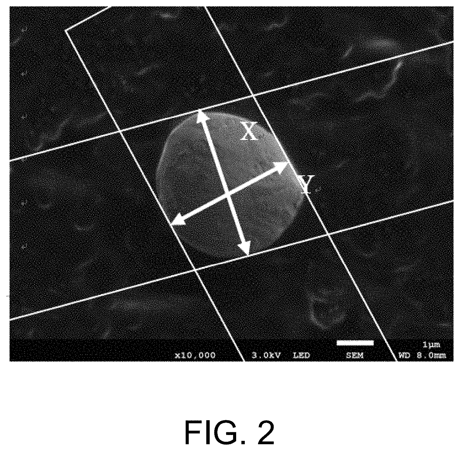
4. The solder particle according to claim 1, wherein a quadrangle circumscribing a projected image of the solder particle is created by two pairs of parallel lines, and distances between opposite sides are set as X and Y, where Y<X, X and Y satisfy the following formula: 0.8<Y/X<1.0.
5. The solder particle according to claim 1, comprising at least one selected from the group consisting of tin, tin alloys, indium and indium alloys.
6. The solder particle according to claim 5, comprising at least one selected from the group consisting of In--Sn alloys, In--Sn--Ag alloys, In--Bi alloys, Sn--Au alloys, Sn--Bi alloys, Sn--Bi--Ag alloys, Sn--Ag--Cu alloys and Sn--Cu alloys.
7. The solder particle according to claim 2, wherein a ratio (A/B) of a diameter A of the flat portion to a diameter B of the solder particle satisfies the following formula: 0.01<A/B<1.0.
8. The solder particle according to claim 2, wherein a quadrangle circumscribing a projected image of the solder particle is created by two pairs of parallel lines, and distances between opposite sides are set as X and Y, where Y<X, X and Y satisfy the following formula: 0.8<Y/X<1.0.
9. The solder particle according to claim 3, wherein a quadrangle circumscribing a projected image of the solder particle is created by two pairs of parallel lines, and distances between opposite sides are set as X and Y, where Y<X, X and Y satisfy the following formula: 0.8<Y/X<1.0.
10. The solder particle according to claim 7, wherein a quadrangle circumscribing a projected image of the solder particle is created by two pairs of parallel lines, and distances between opposite sides are set as X and Y, where Y<X, X and Y satisfy the following formula: 0.8<Y/X<1.0.
11. The solder particle according to claim 2, comprising at least one selected from the group consisting of tin, tin alloys, indium and indium alloys.
12. The solder particle according to claim 3, comprising at least one selected from the group consisting of tin, tin alloys, indium and indium alloys.
13. The solder particle according to claim 4, comprising at least one selected from the group consisting of tin, tin alloys, indium and indium alloys.
14. The solder particle according to claim 7, comprising at least one selected from the group consisting of tin, tin alloys, indium and indium alloys.
15. The solder particle according to claim 8, comprising at least one selected from the group consisting of tin, tin alloys, indium and indium alloys.
16. The solder particle according to claim 9, comprising at least one selected from the group consisting of tin, tin alloys, indium and indium alloys.
17. The solder particle according to claim 10, comprising at least one selected from the group consisting of tin, tin alloys, indium and indium alloys.
18. The solder particle according to claim 11, comprising at least one selected from the group consisting of In--Sn alloys, In--Sn--Ag alloys, In--Bi alloys, Sn--Au alloys, Sn--Bi alloys, Sn--Bi--Ag alloys, Sn--Ag--Cu alloys and Sn--Cu alloys.
19. The solder particle according to claim 12, comprising at least one selected from the group consisting of In--Sn alloys, In--Sn--Ag alloys, In--Bi alloys, Sn--Au alloys, Sn--Bi alloys, Sn--Bi--Ag alloys, Sn--Ag--Cu alloys and Sn--Cu alloys.
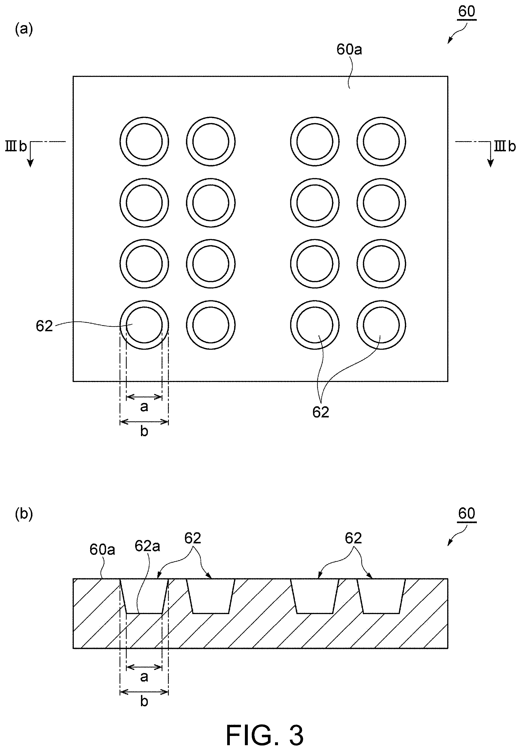
20. The solder particle according to claim 13, comprising at least one selected from the group consisting of In--Sn alloys, In--Sn--Ag alloys, In--Bi alloys, Sn--Au alloys, Sn--Bi alloys, Sn--Bi--Ag alloys, Sn--Ag--Cu alloys and Sn--Cu alloys.
Description
TECHNICAL FIELD
[0001] The present invention relates to solder particles.
BACKGROUND ART
[0002] In the related art, use of solder particles as conductive particles mixed into anisotropic conductive materials such as anisotropic conductive films and anisotropic conductive pastes has been studied. For example, in Patent Literature 1, a conductive paste containing a thermosetting component and a plurality of solder particles subjected to a specific surface treatment is described.
REFERENCE LIST
Patent Literature
[0003] Patent Literature 1: Japanese Patent Laid-Open No. 2016-76494
SUMMARY OF INVENTION
Technical Problem
[0004] In recent years, connecting parts have been miniaturized further, and as the definition of circuit members has become higher, the conduction reliability and the insulation reliability required for anisotropic conductive materials have increased. In order to secure conduction reliability and insulation reliability, it is necessary for conductive particles mixed into an anisotropic conductive material to allow appropriate electrical connection between electrodes that face each other, but it is currently not always possible to realize this with an anisotropic conductive material containing solder particles in the related art.
[0005] The present invention has been made in view of the above circumstances, and an objective of the present invention is to provide solder particles that allow an anisotropic conductive material having excellent conduction reliability and insulation reliability to be obtained.
Solution to Problem
[0006] One aspect of the present invention relates to solder particles having a flat portion on a part of the surface. When such solder particles are used, it is possible to obtain an anisotropic conductive material having excellent conduction reliability and insulation reliability.
[0007] In one aspect, the average particle diameter of the solder particles may be 1 to 30 .mu.m and the C.V. value may be 20% or less.
[0008] In one aspect, a ratio (A/B) of a diameter A of the flat portion to a diameter B of the solder particles may satisfy the following formula:
0.01<A/B<1.0.
[0009] In one aspect, a quadrangle circumscribing a projected image of a solder particle is created by two pairs of parallel lines, and distances between opposite sides are set as X and Y (where Y<X), X and Y may satisfy the following formula:
0.8<Y/X<1.0.
[0010] In one aspect, the solder particles may include at least one selected from the group consisting of tin, tin alloys, indium and indium alloys.
[0011] In one aspect, the solder particles may include at least one selected from the group consisting of In--Sn alloys, In--Sn--Ag alloys, In--Bi alloys, Sn--Au alloys, Sn--Bi alloys, Sn--Bi--Ag alloys, Sn--Ag--Cu alloys and Sn--Cu alloys.
Advantageous Effects of Invention
[0012] According to the present invention, there are provided solder particles that allow an anisotropic conductive material having excellent conduction reliability and insulation reliability to be obtained.
BRIEF DESCRIPTION OF DRAWINGS
[0013] FIG. 1 is a diagram schematically showing an example of solder particles.
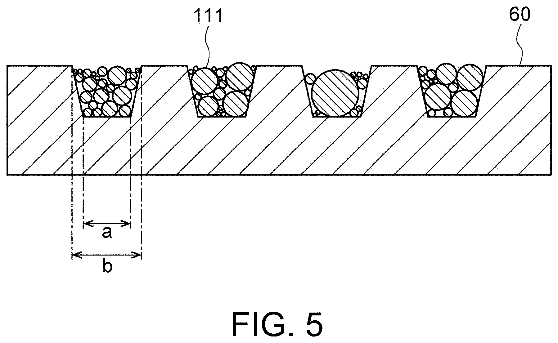
[0014] FIG. 2 is a diagram showing distances X and Y (where Y.ltoreq.X) between opposite sides when a quadrangle circumscribing a projected image of a solder particle is created by two pairs of parallel lines.
[0015] (a) of FIG. 3 is a plan view schematically showing an example of a base material and (b) of FIG. 3 is a cross-sectional view taken along the line IIIb-IIIb shown in (a) of FIG. 3.
[0016] (a) of FIG. 4 to (d) of FIG. 4 are cross-sectional views schematically showing an example of a cross-sectional shape of recesses of the base material.
[0017] FIG. 5 is a cross-sectional view schematically showing a state in which solder fine particles are accommodated in recesses of the base material.
[0018] FIG. 6 is a cross-sectional view schematically showing a state in which solder particles are formed in recesses of the base material.
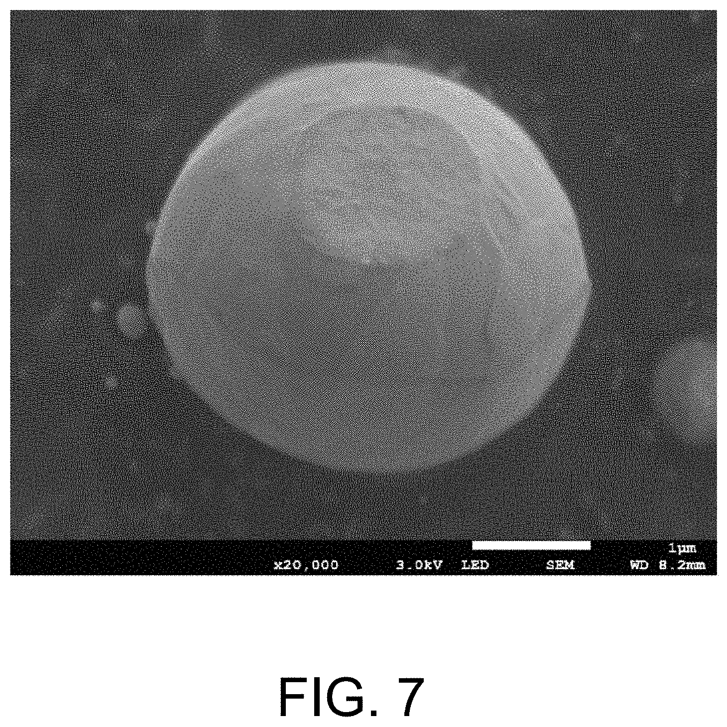
[0019] FIG. 7 is an SEM image of solder particles obtained in Example 1.
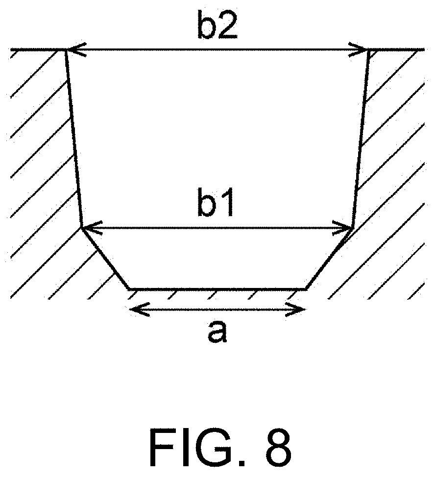
[0020] FIG. 8 is a cross-sectional view schematically showing another example of a cross-sectional shape of the recess of the base material.
DESCRIPTION OF EMBODIMENTS
[0021] Hereinafter, embodiments of the present invention will be described. The present invention is not limited to the following embodiments. Here, unless otherwise specified, materials exemplified below may be used alone or two or more thereof may be used in combination. When there are a plurality of substances corresponding to components in a composition, the content of the components in the composition means a total amount of the plurality of substances present in the composition unless otherwise specified. A numerical range indicated using "to" means a range including numerical values stated before and after "to" as a minimum value and a maximum value. In the numerical ranges described stepwise in this specification, an upper limit value or a lower limit value of a certain stepwise numerical range may be replaced with an upper limit value or a lower limit value of other stepwise numerical ranges. In the numerical ranges described in this specification, the upper limit value or the lower limit value of the numerical range may be replaced with values shown in examples.
<Solder Particles>
[0022] The solder particles according to the present embodiment have a flat portion on a part of the surface. In this case, a surface other than the flat portion preferably has a spherical crown shape. That is, the solder particles may have a flat portion and a spherical crown-shaped curved surface. When an anisotropic conductive material is obtained using such solder particles, it is possible to realize excellent conduction reliability and insulation reliability. The reason for this will be described below.
[0023] First, when a flat portion of solder particles comes in contact with an electrode, a large contact area can be secured between the flat portion and the electrode. For example, when an electrode made of a material which solder easily wets and spread on and an electrode made of a material which solder does not easily wet and spread on are connected, the connection between the two electrodes can be suitably performed by performing adjustment so that flat portions of the solder particles are arranged on the side of the latter electrode.
[0024] In addition, when a contact area between the solder particles and the electrodes is larger, the solder wets and spreads more easily. For example, regarding a method for allowing solder particles disposed on an electrode (substrate) to wet and spread on the electrode, there is a method in which a flux is applied to solder particles themselves or onto an electrode in advance and the solder particles are dissolved by reflowing (heating). At this time, in the case of an oxide film of the solder particles is thick and the flux is weak or the like, when a contact area between the solder particles and the electrodes is small, the solder does not easily wet and spread. On the other hand, when a flat portion is formed on a part of the surface of solder particles, a contact area between the electrodes and the solder particles becomes larger, and wetting and spreading tend to easily occur. This is considered to be because, when removal of the oxide film is in progress and the electrodes and the surface of the solder particles come in contact, the thinned oxide film becomes cracked, the dissolved solder or flux flows, and the oxide film is easily removed. In this manner, when a contact area between the solder particles and the electrodes becomes larger, since the number of contact points between the electrodes and the surface of the solder particles increases, the time at which wetting and spreading occur becomes earlier and wetting and spreading easily occur. Here, since the solder particles easily wet and spread, the amount of flux can be reduced and the occurrence of ion migration due to residual flux can be curbed.
[0025] In addition, since solder particles having a flat portion have a favorable fitting ability, when the solder particles are disposed on the electrode so that the flat portion is in contact with the electrode, the stable shape makes it difficult for the solder particles to be displaced. That is, it is easy to prevent the solder particles from rolling off of the electrodes before reflow, which causes a decrease in conduction reliability between electrodes that face each other and a decrease in insulation reliability between adjacent electrodes.
[0026] FIG. 1 is a diagram schematically showing an example of solder particles 1 according to the present embodiment. As shown in FIG. 1, the solder particles 1 have a shape in which a flat portion 11 having a diameter A is formed on a part of the surface of a sphere having a diameter B. In order to realize excellent conduction reliability and insulation reliability, the ratio (A/B) of the diameter A of the flat portion to the diameter B of the solder particles 1 may be, for example, more than 0.01 and less than 1.0 (0.01<A/B<1.0), and may be 0.1 to 0.9. The diameter B of the solder particles and the diameter A of the flat portion can be observed using, for example, a scanning electron microscope.
[0027] Specifically, an arbitrary particle is observed under a scanning electron microscope and an image is captured. The diameter B of the solder particle and the diameter A of the flat portion are measured from the obtained image, and A/B of the particle is obtained. This operation is performed on 300 solder particles, and an average value is calculated and used as A/B of the solder particles.
[0028] The solder particles 1 may have an average particle diameter of 1 to 30 .mu.m and a C.V. value of 20% or less. Such solder particles have both a small average particle diameter and a narrow particle size distribution, and can be suitably used as conductive particles applied to an anisotropic conductive material having high conduction reliability and insulation reliability.
[0029] The average particle diameter of the solder particles is not particularly limited as long as it is within the above range, and is preferably 30 .mu.m or less, more preferably 25 .mu.m or less, and still more preferably 20 .mu.m or less. In addition, the average particle diameter of the solder particles is preferably 1 .mu.m or more, more preferably 2 .mu.m or more, and still more preferably 4 .mu.m or more.
[0030] The average particle diameter of the solder particles can be measured using various methods according to the size. Methods such as, for example, a dynamic light scattering method, a laser diffraction method, a centrifugal sedimentation method, an electrical detection band method, and a resonance type mass measurement method, can be used. In addition, a method of measuring a particle size from an image obtained by an optical microscope, an electron microscope or the like can be used. Examples of specific devices include a flow type particle image analyzing device, a Microtrac, and a Coulter counter.
[0031] In order to realize better conduction reliability and insulation reliability, the C.V. value of the solder particles is preferably 20% or less, more preferably 10% or less, still more preferably 7% or less, and most preferably 5% or less. In addition, the lower limit of the C.V. value of the solder particles is not particularly limited.
[0032] For example, the C.V. value of the solder particles may be 1% or more or 2% or more.
[0033] The C.V. value of the solder particles is calculated by multiplying a value obtained by dividing the standard deviation of the particle diameter measured by the above method by the average particle diameter by 100.
[0034] When a quadrangle circumscribing a projected image of a solder particle is created by two pairs of parallel lines and distances between opposite sides are set as X and Y (where Y<X), the ratio (Y/X) of Y to X may be more than 0.8 and less than 1.0 (0.8<Y/X<1.0) or may be 0.81 to 0.99. Such solder particles can then be particles closer to true spheres. In the case of the solder particles are accommodated in recesses 62 of a base material 60 again, when the solder particles are close to spherical shapes, they tend to be easily accommodatable. In addition, since the solder particles are close to true spheres, when a plurality of electrodes that face each other are electrically connected via the solder particles, the contact between the solder particles and the electrodes is less likely to be uneven, and a stable connection tends to be obtained. In addition, when a conductive film or paste in which solder particles are dispersed in a resin material is produced, high dispersibility is obtained and dispersion stability during production tends to be obtained. In addition, in a case of a film or paste in which solder particles are dispersed in a resin material is used for connection between electrodes, even if the solder particles rotate in the resin, when the solder particles have a spherical shape, projected areas of the solder particles are close to each other when viewed in a projected image. Therefore, a stable electrical connection with little variation during connection of electrodes tends to be obtained.
[0035] FIG. 2 is a diagram showing distances X and Y between opposite sides (where Y<X) when a quadrangle circumscribing a projected image of a solder particle is created by two pairs of parallel lines. For example, an arbitrary particle may be observed under a scanning electron microscope and a projected image is obtained. Two pairs of parallel lines are drawn on the obtained projected image, one pair of parallel lines is arranged at a position at which the distance between the parallel lines is a minimum, the other pair of parallel lines is arranged at a position at which the distance between the parallel lines is a maximum, and Y/X of the particles is obtained. This operation is performed on 300 solder particles, and an average value is calculated and used as Y/X of the solder particles.
[0036] The solder particles may contain tin or a tin alloy. Regarding the tin alloy, for example, In--Sn alloys, In--Sn--Ag alloys, Sn--Au alloys, Sn--Bi alloys, Sn--Bi--Ag alloys, Sn--Ag--Cu alloys, and Sn--Cu alloys can be used. Specific examples of these tin alloys include the following examples. [0037] In--Sn (In 52 mass %, Bi 48 mass %, melting point 118.degree. C.) [0038] In--Sn--Ag (In 20 mass %, Sn 77.2 mass %, Ag 2.8 mass %, melting point of 175.degree. C.) [0039] Sn--Bi (Sn 43 mass %, Bi 57 mass %, melting point of 138.degree. C.) [0040] Sn--Bi--Ag (Sn 42 mass %, Bi 57 mass %, Ag 1 mass %, melting point of 139.degree. C.) [0041] Sn--Ag--Cu (Sn 96.5 mass %, Ag 3 mass %, Cu 0.5 mass %, melting point of 217.degree. C.) [0042] Sn--Cu (Sn 99.3 mass %, Cu 0.7 mass %, melting point of 227.degree. C.) [0043] Sn--Au (Sn 21.0 mass %, Au 79.0 mass %, melting point of 278.degree. C.)
[0044] The solder particles may contain indium or an indium alloy. Regarding the indium alloy, for example, In--Bi alloys and In--Ag alloys can be used. Specific examples of these indium alloys include the following examples. [0045] In--Bi (In 66.3 mass %, Bi 33.7 mass %, melting point of 72.degree. C.) [0046] In--Bi (In 33.0 mass %, Bi 67.0 mass %, melting point of 109.degree. C.) [0047] In--Ag (In 97.0 mass %, Ag 3.0 mass %, melting point of 145.degree. C.)
[0048] The tin alloy or indium alloy can be selected according to applications of the solder particles (temperature during use). For example, when solder particles are used for fusion at a low temperature, In--Sn alloys and Sn--Bi alloys may be used, and in this case, solder particles can be fused at 150.degree. C. or lower. When a material having a high melting point such as Sn--Ag--Cu alloys and Sn--Cu alloys is used, it is possible to maintain high reliability even after being left at a high temperature.
[0049] The solder particles may contain at least one selected from among Ag, Cu, Ni, Bi, Zn, Pd, Pb, Au, P and B. Among these elements, Ag or Cu may be contained in consideration of the following aspect. That is, when the solder particles contain Ag or Cu, the melting point of the solder particles can be lowered to about 220.degree. C. and the bond strength with respect to an electrode is further improved, and thus more favorable conduction reliability is easily obtained.
[0050] The Cu content of the solder particles is, for example, 0.05 to 10 mass %, and may be 0.1 to 5 mass % or 0.2 to 3 mass %. When the Cu content is 0.05 mass % or more, more favorable solder connection reliability is easily achieved. In addition, when the Cu content is 10 mass % or less, solder particles having a low melting point and excellent wettability are easily obtained, and as a result, the reliability of connection of the bonding part to the solder particles tends to be favorable.
[0051] The Ag content of the solder particles is, for example, 0.05 to 10 mass %, and may be 0.1 to 5 mass % or 0.2 to 3 mass %. When the Ag content is 0.05 mass % or more, more favorable solder connection reliability is easily achieved. In addition, when the Ag content is 10 mass % or less, solder particles having a low melting point and excellent wettability are easily obtained, and as a result, the reliability of connection of the bonding part to the solder particles tends to be favorable.
[0052] The applications of the solder particles are not particularly limited, and for example, the solder particles can be suitably used as conductive particles for an anisotropic conductive material. In addition, the solder particles can be suitably used for applications such as electrically connecting electrodes in a ball grid array connection method (BGA connection) that is widely used for mounting a semiconductor integrated circuit and applications such as sealing components such as a microelectro mechanical system (MEMS) and pipe sealing, brazing, and height and clearance control spacers. That is, the solder particles can be used for general applications in which conventional solder is used.
<Method for Producing Solder Particles>
[0053] A method for producing solder particles according to the present embodiment is not particularly limited, and an example of the production method will be described below. For example, solder particles according to the present embodiment can be produced by a method for producing solder particles including a preparation step in which a base material having a plurality of recesses and solder fine particles are prepared, an accommodation step in which at least some of the solder fine particles are accommodated in the recesses of the base material, and a fusing step in which the solder fine particles accommodated in the recesses are fused and the solder particles are formed inside the recesses. According to this production method, solder particles having a flat portion on a part of the surface are produced.
[0054] A method for producing solder particles will be described below with reference to FIGS. 3 to 6.
[0055] First, solder fine particles and a base material 60 in which solder fine particles are contained are prepared. (a) of FIG. 3 is a plan view schematically showing an example of the base material 60 and (b) of FIG. 3 is a cross-sectional view taken along the line IIIb-IIIb shown in (a) of FIG. 3. The base material 60 shown in (a) of FIG. 3 has a plurality of recesses 62. The plurality of recesses 62 may be regularly arranged in a predetermined pattern. In this case, after solder particles are formed in the recesses 62, the solder particles in the recesses 62 are transferred to a resin material or the like, and thus the solder particles can be regularly arranged.
[0056] The recesses 62 of the base material 60 are preferably formed in a tapered shape in which an opening area enlarges from the side of a bottom 62a of the recesses 62 toward the side of a surface 60a of the base material 60. That is, as shown in FIG. 3, the width (a width a in FIG. 3) of the bottom 62a of the recesses 62 is preferably narrower than the width (a width b in FIG. 3) of an opening on the surface 60a of the recesses 62. In addition, the size (a width a, a width b, a volume, a taper angle, a depth, etc.) of the recesses 62 may be set according to the size of desired solder particles.
[0057] Here, the shape of the recesses 62 may be a shape other than the shape shown in FIG. 3. For example, the shape of the opening on the surface 60a of the recesses 62 may be an ellipse, a triangle, a quadrangle, a polygon or the like, in addition to a circle as shown in FIG. 3.
[0058] In addition, the shape of the recesses 62 in the cross section perpendicular to the surface 60a may be, for example, a shape shown in FIG. 4. (a) of FIG. 4 to (d) of FIG. 4 are cross-sectional views schematically showing an example of a cross-sectional shape of the recess of the base material. The bottom surface of each of the cross-sectional shapes shown in (a) of FIG. 4 to (d) of FIG. 4 is flat. Thereby, a flat portion is formed on a part of the surface of the solder particles. In addition, in any of the cross-sectional shapes shown in (a) of FIG. 4 to (d) of FIG. 4, the width (the width b) of the opening on the surface 60a of the recesses 62 is the maximum width in the cross-sectional shape. Thereby, it is easy to remove the solder particles formed in the recesses 62, and thus the workability is improved.
[0059] Regarding the material constituting the base material 60, for example, an inorganic material such as silicon, various ceramics, glass, and a metal such as stainless steel, and an organic material such as various resins can be used. Among these, the base material 60 is preferably formed of a heat-resistant material that does not deteriorate at a melting temperature of the solder fine particles. In addition, the recesses 62 of the base material 60 can be formed by a known method such as a photolithography method, an imprint method, a machining method, an electron beam processing method, and a radiation processing method.
[0060] The solder fine particles prepared in the preparation step may include fine particles having a particle diameter smaller than the width (the width b) of the opening on the surface 60a of the recesses 62, and preferably include more fine particles having a particle diameter smaller than the width b. For example, in the solder fine particles, the D10 particle diameter of the particle size distribution is preferably smaller than the width b, the D30 particle diameter of the particle size distribution is more preferably smaller than the width b, and the D50 particle diameter of the particle size distribution is still more preferably smaller than the width b.
[0061] The particle size distribution of the solder fine particles can be measured using various methods according to the size. Methods, for example, a dynamic light scattering method, a laser diffraction method, a centrifugal sedimentation method, an electrical detection band method, and a resonance type mass measurement method, can be used. In addition, a method of measuring a particle size from an image obtained by an optical microscope, an electron microscope or the like can be used. Examples of specific devices include a flow type particle image analyzing device, a Microtrac, and a Coulter counter.
[0062] The C.V. value of the solder fine particles prepared in the preparation step is not particularly limited, and in order to improve filling into the recesses 62 according to a combination of large and small fine particles, a high C.V. value is preferable. For example, the C.V. value of the solder fine particles may be more than 20%, and is preferably 25% or more and more preferably 30% or more.
[0063] The C.V. value of the solder fine particles is calculated by multiplying a value obtained by dividing the standard deviation of particle diameters measured by the above method by the average particle diameter (D50 particle diameter) by 100.
[0064] The solder fine particles may contain tin or a tin alloy. Regarding the tin alloy, for example, In--Sn alloys, In--Sn--Ag alloys, Sn--Au alloys, Sn--Bi alloys, Sn--Bi--Ag alloys, Sn--Ag--Cu alloys, and Sn--Cu alloys can be used. Specific examples of these tin alloys include the following examples. [0065] In--Sn (In 52 mass %, Bi 48 mass %, melting point of 118.degree. C.) [0066] In--Sn--Ag (In 20 mass %, Sn 77.2 mass %, Ag 2.8 mass %, melting point of 175.degree. C.) [0067] Sn--Bi (Sn 43 mass %, Bi 57 mass %, melting point of 138.degree. C.) [0068] Sn--Bi--Ag (Sn 42 mass %, Bi 57 mass %, Ag 1 mass %, melting point of 139.degree. C.) [0069] Sn--Ag--Cu (Sn 96.5 mass %, Ag 3 mass %, Cu 0.5 mass %, melting point of 217.degree. C.) [0070] Sn--Cu (Sn 99.3 mass %, Cu 0.7 mass %, melting point of 227.degree. C.) [0071] Sn--Au (Sn 21.0 mass %, Au 79.0 mass %, melting point of 278.degree. C.)
[0072] The solder particles may contain indium or an indium alloy. Regarding the indium alloy, for example, In--Bi alloys and In--Ag alloys can be used. Specific examples of these indium alloys include the following examples. [0073] In--Bi (In 66.3 mass %, Bi 33.7 mass %, melting point of 72.degree. C.) [0074] In--Bi (In 33.0 mass %, Bi 67.0 mass %, melting point of 109.degree. C.) [0075] In--Ag (In 97.0 mass %, Ag 3.0 mass %, melting point of 145.degree. C.)
[0076] The tin alloy or indium alloy can be selected according to applications of the solder particles (temperature during use). For example, when it is desired to obtain solder particles used for fusion at a low temperature, In--Sn alloys and Sn--Bi alloys may be used, and in this case, solder particles that can be fused at 150.degree. C. or lower are obtained. When a material having a high melting point such as Sn--Ag--Cu alloys and Sn--Cu alloys is used, solder particles that can maintain high reliability even after being left at a high temperature can be obtained.
[0077] The solder fine particles may contain at least one selected from among Ag, Cu, Ni, Bi, Zn, Pd, Pb, Au, P and B. Among these elements, Ag or Cu may be contained in consideration of the following aspect. That is, when the solder fine particles contain Ag or Cu, effects in which the melting point of the obtained solder particles can be lowered to about 220.degree. C. and the solder particles having an excellent bond strength with respect to an electrode are obtained, and thus favorable conduction reliability is obtained are obtained.
[0078] The Cu content of the solder fine particles is, for example, 0.05 to 10 mass %, and may be 0.1 to 5 mass % or 0.2 to 3 mass %. When the Cu content is 0.05 mass % or more, it is easy to obtain solder particles that allow favorable solder connection reliability to be achieved. In addition, when the Cu content is 10 mass % or less, solder particles having a low melting point and excellent wettability are easily obtained, and as a result, the reliability of connection of the bonding part to the solder particles tends to be favorable.
[0079] The Ag content of the solder fine particles is, for example, 0.05 to 10 mass %, and may be 0.1 to 5 mass % or 0.2 to 3 mass %. When the Ag content is 0.05 mass % or more, it is easy to obtain solder particles that allow favorable solder connection reliability to be achieved. In addition, when the Ag content is 10 mass % or less, solder particles having a low melting point and excellent wettability are easily obtained, and as a result, the reliability of connection of the bonding part to the solder particles tends to be favorable.
[0080] In the accommodation step, the solder fine particles prepared in the preparation step are accommodated in each of the recesses 62 of the base material 60. The accommodation step may be a step in which all of the solder fine particles prepared in the preparation step are accommodated in the recesses 62 or a step in which some of the solder fine particles prepared in the preparation step (for example, those having a diameter smaller than the width b of the opening of the recesses 62 among the solder fine particles) are accommodated in the recesses 62.
[0081] FIG. 5 is a cross-sectional view schematically showing a state in which solder fine particles 111 are accommodated in the recesses 62 of the base material 60. As shown in FIG. 5, the plurality of solder fine particles 111 are accommodated in each of the plurality of recesses 62.
[0082] For example, the amount of the solder fine particles 111 accommodated in the recesses 62 is preferably 20% or more, more preferably 30% or more, still more preferably 50% or more, and most preferably 60% or more with respect to the volume of the recesses 62. Thereby, the variation in the accommodation amount is minimized and solder particles having a smaller particle size distribution are easily obtained.
[0083] A method of accommodating solder fine particles in the recesses 62 is not particularly limited. The accommodation method may be any of a dry type and a wet type. For example, when the solder fine particles prepared in the preparation step are placed on the base material 60 and the surface 60a of the base material 60 is rubbed with a squeegee, excess solder fine particles can be removed and sufficient solder fine particles can be accommodated in the recesses 62. When the width b of the opening of the recesses 62 is larger than the depth of the recesses 62, the solder fine particles protrude from the opening of the recesses 62. When the squeegee is used, the solder fine particles protruding from the opening of the recesses 62 are removed.
[0084] Examples of a method of removing excess solder fine particles include a method of spraying compressed air and a method of rubbing the surface 60a of the base material 60 with a non-woven fabric or fiber bundle. These methods are preferable for handling easily deformable solder fine particles because a physical power is weaker than that of the squeegee. In addition, in these methods, solder fine particles protruding from the opening of the recesses 62 can remain in the recess.
[0085] The fusing step is a step in which the solder particles 111 accommodated in the recesses 62 are fused, and the solder particles 1 are formed inside the recesses 62. FIG. 6 is a cross-sectional view schematically showing a state in which the solder particles 1 are formed in the recesses 62 of the base material 60. The solder fine particles 111 accommodated in the recesses 62 are melted and coalesced, and spheroidized due to surface tension. In this case, at a part in contact with the bottom 62a of the recesses 62, the molten solder forms a flat portion 11 conforming to the bottom 62a. Thereby, the formed solder particles 1 have a shape having a flat portion 11 on a part of the surface.
[0086] FIG. 1 is a diagram of the solder particles 1 when viewed from the side opposite to an opening part of the recesses 62 in FIG. 6.
[0087] Examples of a method of melting the solder fine particles 111 accommodated in the recesses 62 include a method of heating the solder fine particles 111 to a melting point of the solder or higher. Due to the influence of an oxide film, even if heated to a temperature equal to or higher than the melting point, the solder fine particles 111 may not melt, may not wet and spread, or may not coalesce. Therefore, when the solder fine particles 111 are exposed to a reducing atmosphere, the oxide film on the surface of the solder fine particles 111 is removed and heating is then performed at a temperature equal to or higher than the melting point of the solder fine particles 111, and the solder fine particles 111 can be melted, wet and spread, and be coalesced. In addition, the solder fine particles 111 are preferably melted under a reducing atmosphere. When the solder fine particles 111 are heated to a temperature equal to or higher than the melting point of the solder fine particles 111 and a reducing atmosphere is created, the oxide film on the surface of the solder fine particles 111 is reduced, and the solder fine particles 111 are efficiently and easily melted, wet and spread, and be coalesced.
[0088] The method of creating a reducing atmosphere is not particularly limited as long as the above effects are obtained, and for example, a method using hydrogen gas, hydrogen radicals, formic acid gas, or the like may be used. For example, the solder fine particles 111 can be melted under a reducing atmosphere using a hydrogen reduction furnace, a hydrogen radical reduction furnace, a formic acid reduction furnace, or a conveyor furnace or a consecutive series of such furnaces. In these devices, the furnace may include a heating device, a chamber filled with an inert gas (nitrogen, argon, etc.), a mechanism for evacuating the inside of the chamber and the like, and thereby a reducing gas is more easily controlled. In addition, when the inside of the chamber can be evacuated, after the solder fine particles 111 are melted and coalesced, voids can be removed due to a reduced pressure, and the solder particles 1 having superior connection stability can be obtained.
[0089] Profiles such as reducing and dissolving conditions for the solder fine particles 111, the temperature, and adjustment of the atmosphere in the furnace may be appropriately set in consideration of the melting point of the solder fine particles 111, the particle size, the size of the recesses, and the material of the base material 60. For example, the base material 60 in which the solder fine particles 111 are filled into recesses is inserted into a furnace, the furnace is evacuated, a reducing gas is then introduced, the inside of the furnace is filled with a reducing gas, the oxide film on the surface of the solder fine particles 111 is removed, the reducing gas is then removed by evacuation, heating is then performed to a temperature equal to or higher than the melting point of the solder fine particles 111, the solder fine particles are dissolved and coalesced, the solder particles are formed in the recesses 62, the temperature in the furnace is then returned to room temperature after filling with nitrogen gas, and thus the solder particles 1 can be obtained. In addition, for example, the base material 60 in which the solder fine particles 111 are filled into recesses is inserted into a furnace, the furnace is evacuated, a reducing gas is then introduced, the inside of the furnace is filled with a reducing gas, the solder fine particles 111 are heated by a heating heater in the furnace, the oxide film on the surface of the solder fine particles 111 is removed, the reducing gas is then removed by evacuation, heating is then performed to a temperature equal to or higher than the melting point of the solder fine particles 111, the solder fine particles are dissolved and coalesced, the solder particles are formed in the recesses 62, the temperature in the furnace is then returned to room temperature after filling with nitrogen gas, and thus the solder particles 1 can be obtained. When the solder fine particles are heated under a reducing atmosphere, there are advantages that the reducing power increases and the oxide film on the surface of the solder fine particles is easily removed.
[0090] In addition, for example, the base material 60 in which the solder fine particles 111 are filled into recesses is inserted into a furnace, the furnace is evacuated, a reducing gas is then introduced, the inside of the furnace is filled with a reducing gas, the base material 60 is heated to a temperature equal to or higher than the melting point of the solder fine particles 111 by a heating heater in the furnace, the oxide film on the surface of the solder fine particles 111 is removed by reduction, and at the same time, the solder fine particles are dissolved and coalesced, the solder particles are formed in the recesses 62, the reducing gas is removed by evacuation, and additionally, the number of voids in the solder particles is reduced, the temperature in the furnace is then returned to room temperature after filling with nitrogen gas, and thus the solder particles 1 can be obtained. In this case, since it is easy to adjust the increase and decrease of the temperature in the furnace once, there is an advantage that processing can be performed in a short time.
[0091] A step in which the inside of the furnace is made into a reducing atmosphere again and the oxide film on the surface that has not been completely removed is removed after the solder particles are formed in the recesses 62 may be additionally performed, and it is thus possible to reduce the amount of residue such as remaining unfused solder fine particles and a part of the unfused remaining oxide film.
[0092] When an atmospheric pressure conveyor furnace is used, the base material 60 in which the solder fine particles 111 are filled into recesses is placed on a transport conveyor and is caused to pass through a plurality of zones consecutively, and thus the solder particles 1 can be obtained. For example, the base material 60 in which the solder fine particles 111 are filled into recesses is placed on a conveyor set at a certain speed and caused to pass through a zone filled with an inert gas such as nitrogen or argon with a temperature lower than the melting point of the solder fine particles 111 and subsequently pass through a zone in which a reducing gas such as formic acid gas with a temperature lower than the melting point of the solder fine particles 111 is provided, the oxide film on the surface of the solder fine particles 111 is removed, and subsequently the material is caused to pass through a zone filled with an inert gas such as nitrogen and argon with a temperature equal to or higher than the melting point of the solder fine particles 111, the solder fine particles 111 are melted and coalesced, and subsequently the material is caused to pass through a cooling zone filled with an inert gas such as nitrogen and argon, and thus the solder particles 1 can be obtained. For example, the base material 60 in which the solder fine particles 111 are filled into recesses is placed on a conveyor set at a certain speed and caused to pass through a zone filled with an inert gas such as nitrogen and argon with a temperature equal to or higher than the melting point of the solder fine particles 111, subsequently pass through a zone in which a reducing gas such as formic acid gas with a temperature equal to or higher than the melting point of the solder fine particles 111 is provided, the oxide film on the surface of the solder fine particles 111 is removed, and melting and coalescing are performed, subsequently the material is caused to pass through a cooling zone filled with an inert gas such as nitrogen and argon, and thus the solder particles 1 can be obtained. Since the above conveyor furnace can perform processing at atmospheric pressure, it is possible to continuously process a film-like material in a roll to roll method. For example, a continuous roll product of the base material 60 in which the solder fine particles 111 are filled into recesses is produced, a roller unwinding machine is installed on the inlet side of the conveyor furnace, a roller winding machine is installed on the exit side of the conveyor furnace, the base material 60 is transported at a certain speed and caused to pass through zones in the conveyor furnace, and thus the solder fine particles 111 filled into the recesses can be fused.
[0093] The formed solder particles 1 that are accommodated in the recesses 62 of the base material 60 may be transported or stored, and the formed solder particles 1 may be removed from the recesses 62 and collected.
[0094] In addition, a resin material is disposed on the surface 60a of the base material 60, and the solder particles 1 in the recesses 62 may be transferred to the resin material. In this case, when the recesses 62 are regularly arranged, the solder particles 1 can be regularly arranged on the resin material. In addition, in this case, the flat portion of the arranged solder particles 1 can be maintained in one direction. Therefore, the flat portions are effectively used during electrode connection, and as described above, it is easy to obtain advantages that a large contact area between the solder particles and the electrode is secured, and displacement of the solder particles is minimized.
[0095] According to the production method of the present embodiment, it is possible to form solder particles having a uniform size regardless of the material and shape of the solder fine particles. For example, indium-based solder can be precipitated by plating, but is unlikely to be precipitated in the form of particles and is hard to handle because it is soft. However, in the production method of the present embodiment, it is possible to easily produce indium-based solder particles having a uniform particle diameter using indium-based solder fine particles as a raw material. In addition, since the formed solder particles 1 that are accommodated in the recesses 62 of the base material 60 can be handled, the solder particles can be transported and stored without being deformed. In addition, since the formed solder particles 1 are simply accommodated in the recesses 62 of the base material 60, they can be easily removed, and the solder particles can be collected and subjected to a surface treatment and the like without being deformed.
[0096] In addition, the solder fine particles 111 may have a large variation in the particle size distribution or may have a distorted shape but can be used as a raw material in the production method of the present embodiment as long as they can be accommodated in the recesses 62.
[0097] In addition, in the production method of the present embodiment, in the base material 60, the shape of the recesses 62 can be freely designed according to a lithography method, an imprint method, an electron beam processing method, a radiation processing method, a machining method, or the like. Since the size of the solder particles 1 depends on the amount of the solder fine particles 111 accommodated in the recesses 62, in the production method of the present embodiment, the size of the solder particles 1 can be freely designed according to designing of the recesses 62.
[0098] While preferred embodiments of the present invention have been described above, the present invention is not limited to the above embodiments.
EXAMPLES
[0099] The present invention will be described below in more detail with reference to examples, but the present invention is not limited to these examples.
<Production of Solder Particles>
Example 1
(Step a1: Classification of Solder Fine Particles)
[0100] 100 g of Sn--Bi solder fine particles (Type 8 commercially available from 5N Plus, a melting point of 139.degree. C.), were immersed in distilled water and ultrasonically dispersed and then left, and the solder fine particles suspended in the supernatant were collected. This operation was repeated, and 10 g of the solder fine particles were collected. The average particle diameter of the obtained solder fine particles was 1.0 .mu.m, and the C.V. value was 42%.
(Step b1: Disposition in Base Material)
[0101] A base material (polyimide film, a thickness of 100 .mu.m) having a plurality of recesses with an opening diameter of 1.2 .mu.m.phi., a bottom diameter of 1.0 .mu.m.phi., and a depth of 1.0 .mu.m (when the opening part was viewed from the top, the bottom diameter of 1.0 .mu.m.phi. corresponded to the opening diameter of 1.2 .mu.m.phi. at the center) was prepared. The plurality of recesses were regularly arranged at intervals of 1.0 .mu.m. The solder fine particles (with an average particle diameter of 1.0 .mu.m and a C.V. value of 42%) obtained in Step a were disposed in the recesses of the base material. Here, the surface side on which the recesses of the base material were formed was rubbed with a fine adhesive roller, excess solder fine particles were removed, and a base material in which the solder fine particles were disposed only in the recesses was obtained.
(Step c1: Formation of Solder Particles)
[0102] The base material in which the solder fine particles were disposed in the recesses in Step b1 was put into a hydrogen reduction furnace and the furnace was evacuated, hydrogen gas was then introduced into the furnace, and the inside of the furnace was filled with hydrogen. Then, the temperature in the furnace was kept at 280.degree. C. for 20 minutes, the furnace was then evacuated again, nitrogen was introduced to return to atmospheric pressure, the temperature in the furnace was then lowered to room temperature, and thereby solder particles were formed.
[0103] Here, when the base material that had undergone Step c1 was tapped from the back side of the recesses, the solder particles were collected from the recesses. The obtained solder particles were observed according to the following method. The obtained solder particles were placed on a conductive tape fixed to a surface of a pedestal for scanning electron microscope (SEM) observation, the pedestal for SEM observation was tapped on a stainless steel plate with a thickness of 5 mm, and the solder particles spread evenly on the conductive tape. Then, compressed nitrogen gas was sprayed onto the surface of the conductive tape and the solder particles were fixed as a single layer on the conductive tape. The observation results are shown in FIG. 7. FIG. 7 shows an SEM image of a solder particle obtained in Example 1. As shown in FIG. 7, the obtained solder particles had a shape in which a flat portion was formed in a part of surface of the sphere. Here, the solder particles obtained in the other examples also had the same shape.
Examples 2 to 12
[0104] Solder particles were produced in the same manner as in Example 1 except that the size of the recess was changed as shown in Table 1.
Example 13
[0105] Solder particles were produced, collected and evaluated in the same manner as in Example 1 except that the following Step c2 was performed in place of Step c1. The results are shown in Table 2.
(Step c2: Formation of Solder Particles)
[0106] The base material in which the solder fine particles were disposed in the recesses in Step b1 was put into a hydrogen radical reduction furnace (plasma reflow device commercially available from Shinko Seiki Co., Ltd.), the furnace was evacuated, hydrogen gas was introduced into the furnace, and the inside of the furnace was filled with hydrogen gas. Then, the temperature in the furnace was adjusted to 120.degree. C. and hydrogen radicals were emitted for 5 minutes. Then, hydrogen gas in the furnace was removed by evacuation, heating was performed to 170.degree. C., nitrogen was then introduced into the furnace to return to atmospheric pressure, the temperature in the furnace was then lowered to room temperature, and thereby solder particles were formed.
Examples 14 to 24
[0107] Solder particles were produced, collected and evaluated in the same manner as in Example 13 except that the size of the recess was changed as shown in Table 1. The results are shown in Table 2.
Example 25
[0108] Solder particles were produced, collected and evaluated in the same manner as in Example 1 except that the following Step c2 was performed in place of Step c1. The results are shown in Table 2.
(Step c2: Formation of Solder Particles)
[0109] The base material in which the solder fine particles were disposed in the recesses in Step b1 was put into a hydrogen radical reduction furnace (plasma reflow device commercially available from Shinko Seiki Co., Ltd.), the furnace was evacuated, hydrogen gas was introduced into the furnace, and the inside of the furnace was filled with hydrogen gas. Then, the temperature in the furnace was adjusted to 120.degree. C. and hydrogen radicals were emitted for 5 minutes. Then, hydrogen gas in the furnace was removed by evacuation, heating was performed to 145.degree. C., nitrogen was then introduced into the furnace to return to atmospheric pressure, the temperature in the furnace was then lowered to room temperature, and thereby solder particles were formed.
Examples 26 to 36
[0110] Solder particles were produced, collected and evaluated in the same manner as in Example 25 except that the size of the recess was changed as shown in Table 1. The results are shown in Table 2.
<Production of Anisotropic Conductive Film>
Production Example 1
[0111] (Step d1: Filling of Flux into Recesses)
[0112] 10 g of adipic acid was dissolved in 200 g of toluene to prepare a coating solution, and this solution was applied to the base material (transfer mold) in which the solder particles were to be disposed in the recesses in Step c1. Then, the excess coating solution was removed using a squeegee, and the inside of the recesses was filled with the coating solution. This was put into an explosion preventive dryer at 80.degree. C. for 1 minute, toluene was vaporized, and adipic acid as a flux component was thus filled into the recesses.
(Step e1: Production of Adhesive Film)
[0113] 100 g of a phenoxy resin (product name "PKHC" commercially available from Union Carbide Corporation) and 75 g of an acrylic rubber (a copolymer containing 40 parts by mass of butyl acrylate, 30 parts by mass of ethyl acrylate, 30 parts by mass of acrylonitrile, and 3 parts by mass of glycidyl methacrylate, molecular weight: 850,000) were dissolved in 400 g of ethyl acetate to obtain a solution. 300 g of a liquid epoxy resin containing a microcapsule type latent curing agent (an epoxy equivalent of 185, product name "Novacure HX-3941" commercially available from Asahi Kasei Corporation) was added to the solution, and the mixture was stirred to obtain an adhesive solution. The obtained adhesive solution was applied to a separator (silicone-treated polyethylene terephthalate film, a thickness of 40 .mu.m) using a roll coater, and heated at 90.degree. C. for 10 minutes and dried, and adhesive films (insulating resin films) having a thickness of 4 .mu.m, 6 .mu.m, 8 .mu.m, 12 .mu.m and 20 .mu.m were prepared on the separator.
(Step f1: Transfer of Solder Particles)
[0114] The adhesive film formed on the separator and the base material (transfer mold) in which the flux-coated solder particles obtained in Step d1 were disposed were arranged to face each other and the solder particles were transferred to the adhesive film.
(Step g1: Production of Anisotropic Conductive Film)
[0115] The adhesive film produced in the same method as in Step e1 was brought into contact with a transfer surface of the adhesive film obtained in Step f1 and heated and pressurized at 50.degree. C. and 0.1 MPa (1 kgf/cm.sup.2), and an anisotropic conductive film in which the solder particles were disposed in layers in a cross-sectional view of the film, and a flat portion of the solder particles faced only one of the main surfaces of the film was obtained. Here, 4 .mu.m was superimposed for a film with a thickness of 4 .mu.m, and similarly, 6 .mu.m was superimposed for a film with a thickness of 6 .mu.m, 8 .mu.m was superimposed for a film with a thickness of 8 .mu.m, 12 .mu.m was superimposed for a film with a thickness of 12 .mu.m, and 20 .mu.m was superimposed for a film with a thickness of 20 .mu.m, and anisotropic conductive films having a thickness of 8 .mu.m, 12 .mu.m, 16 .mu.m, 24 .mu.m and 40 .mu.m were produced.
[Evaluation of Solder Particles]
[0116] The adhesive film obtained in Step f1 was cut to 10 cm.times.10 cm, Pt sputtering was performed on a surface on which the solder particles were disposed, and observation was then performed using an SEM. 300 solder particles were observed, and the average diameter B (average particle diameter) of the solder particles, the average diameter A of the flat portion, the C.V. value, the roundness, and A/B and Y/X were calculated. The results are shown in Table 2.
Roundness: a ratio r/R of radii of two concentric circles (a radius r of a minimum circumscribed circle, and a radius R of a maximum inscribed circle) of solder particles A/B: a ratio of the diameter A of the flat portion to the diameter B of solder particles Y/X: a ratio of Y to X when distances between opposite sides were set as X and Y (where Y<X), and a quadrangle circumscribing a projected image of a solder particle was created by two pairs of parallel lines
<Production of Connection Structure>
[0117] (Step h1: Preparation of Chip with Copper Bumps)
[0118] Five types of chips with copper bumps (1.7 mm.times.1.7 mm, thickness: 0.5 mm) shown below were prepared. [0119] Chip C1 . . . area 30 .mu.m.times.30 .mu.m, space 30 .mu.m, height: 10 .mu.m, number of bumps 362 [0120] Chip C2 . . . area 15 .mu.m.times.15 .mu.m, space 10 .mu.m, height: 10 .mu.m, number of bumps 362 [0121] Chip C3 . . . area 10 .mu.m.times.10 .mu.m, space 10 .mu.m, height: 7 .mu.m, number of bumps 362 [0122] Chip C4 . . . area 5 .mu.m.times.5 .mu.m, space 6 .mu.m, height: 5 .mu.m, number of bumps 362 [0123] Chip C5 . . . area 3 .mu.m.times.3 .mu.m, space 3 .mu.m, height: 5 .mu.m, number of bumps 362 (Step i1: Preparation of Substrate with Copper Bumps)
[0124] Five types of substrates with copper bumps (thickness: 0.7 mm) shown below were prepared. [0125] Substrate D1 . . . area 30 .mu.m.times.30 .mu.m, space 30 .mu.m, height: 10 .mu.m, number of bumps 362 [0126] Substrate D2 . . . area 15 .mu.m.times.15 .mu.m, space 10 .mu.m, height: 10 .mu.m, number of bumps 362 [0127] Substrate D3 . . . area 10 .mu.m.times.10 .mu.m, space 10 .mu.m, height: 7 .mu.m, number of bumps 362 [0128] Substrate D4 . . . area 5 .mu.m.times.5 .mu.m, space 6 .mu.m, height: 5 .mu.m, number of bumps 362 [0129] Substrate D5 . . . area 3 .mu.m.times.3 .mu.m, space 3 .mu.m, height: 5 .mu.m, number of bumps 362 (Step j1: Connection Between Chip with Copper Bumps and Substrate with Copper Bumps)
[0130] Next, using the anisotropic conductive film produced in Step g1, a chip with copper bumps (1.7 mm.times.1.7 mm, thickness: 0.5 mm) and a substrate with copper bumps (thickness: 0.7 mm) were connected according to the following procedures i) to iii) to obtain a connection structure.
i) A separator (silicone-treated polyethylene terephthalate film, a thickness of 40 .mu.m) on one surface of the anisotropic conductive film (2 mm.times.19 mm) was peeled off, and the anisotropic conductive film and the substrate with copper bumps were brought into contact with each other and bonded at 80.degree. C. and 0.98 MPa (10 kgf/cm.sup.2). ii) A separator on the other surface was peeled off, and the chip with copper bumps was bonded while the bumps of the chip with copper bumps and the bumps of the substrate with copper bumps were aligned. Here, the flat portion of the solder particles faced the side of the substrate with copper bumps. iii) Heating and pressurizing were performed from above the chip under conditions of 180.degree. C., 40 gf/bump, and 30 seconds, and thus connection was performed. A total of seven types of connection structures according to (1) to (7) were produced by combining the following (1) to (7) "chip/anisotropic conductive film/substrate" (1) Chip C1/conductive film with a thickness of 40 .mu.m/substrate D1 (2) Chip C1/conductive film with a thickness of 24 .mu.m/substrate D1 (3) Chip C1/conductive film with a thickness of 16 .mu.m/substrate D1 (4) Chip C2/conductive film with a thickness of 16 .mu.m/substrate D2 (5) Chip C3/conductive film with a thickness of 12 .mu.m/substrate D3 (6) Chip C4/conductive film with a thickness of 8 .mu.m/substrate D4 (7) Chip C5/conductive film with a thickness of 8 .mu.m/substrate D5
Production Examples 2 to 36
[0131] An anisotropic conductive film and a connection structure were produced in the same method as in Production Example 1 except that the base material (transfer mold) in which solder particles were disposed in recesses obtained in Examples 2 to 36 was used.
Comparative Production Example 1
[0132] A solder particles-containing anisotropic conductive paste containing the following components in the following parts by mass was produced.
Polymer: 12 parts by mass Thermosetting compound: 29 parts by mass High dielectric constant curing agent: 20 parts by mass Thermosetting agent: 11.5 parts by mass Flux-coated solder particles: 36 parts by mass (2 parts by mass of flux, 34 parts by mass of solder particles)
[0133] The polymer was prepared as follows.
[0134] Synthesis of a reaction product (polymer A) of bisphenol F, 1,6-hexanediol diglycidyl ether, and a bisphenol F type epoxy resin:
[0135] 72 parts by mass of bisphenol F (containing 4,4'-methylene bisphenol, 2,4'-methylene bisphenol, and 2,2'-methylene bisphenol at a mass ratio of 2:3:1), 70 parts by mass of 1,6-hexanediol diglycidyl ether, and 30 parts by mass of a bisphenol F type epoxy resin ("EPICLON EXA-830CRP" commercially available from DIC) were put into a three-neck flask and dissolved at 150.degree. C. under a nitrogen flow. Then, 0.1 parts by mass of tetra n-butyl sulfonium bromide as an addition reaction catalyst for hydroxy groups and epoxy groups was added, and an addition polymerization reaction was performed at 150.degree. C. for 6 hours under a nitrogen flow to obtain a reaction product (polymer).
[0136] Regarding the thermosetting compound, a resorcinol type epoxy compound ("EX-201" commercially available from Nagase ChemteX Corporation) was used.
[0137] Regarding the high dielectric constant curing agent, pentaerythritol tetrakis(3-mercaptobutyrate) was used.
[0138] Regarding the thermosetting agent, "Karenz MT PE1" (commercially available from Showa Denko K.K.) was used.
[0139] The flux-coated solder particles were prepared as follows. 200 g of SnBi solder particles ("ST-3" commercially available from Mitsu Mining & Smelting Co., Ltd.), 40 g of adipic acid, and 70 g of acetone were weighed out in a three-neck flask, and 0.3 g of dibutyl tin oxide as a dehydration condensation catalyst for hydroxy groups on the surface of solder particle bodies and carboxylic groups of adipic acid was then added thereto and reacted at 60.degree. C. for 4 hours. Then, the solder particles were collected by filtration. The collected solder particles, 50 g of adipic acid, 200 g of toluene, and 0.3 g of para-toluene sulfonic acid were weighed out in a three-neck flask, and reacted at 120.degree. C. for 3 hours while evacuating and refluxing. In this case, the reaction was performed while removing water generated by dehydration condensation using a Dean-Stark extraction device. Then, the solder particles were collected by filtration, washed with hexane and dried. Then, the obtained solder particles were crushed with a ball mill and a sieve was then selected so that a predetermined C.V. value was obtained. The average particle diameter of the obtained SnBi solder particles (flux-coated solder particles) was 4 .mu.m, and the C.V. value was 31%.
[0140] Using the solder particles-containing anisotropic conductive paste, a chip with copper bumps and a substrate with copper bumps were connected in the same manner as in Production Example 1 to produce a connection structure. The solder particles-containing anisotropic conductive paste was applied onto the substrate and the chip was additionally placed thereon. The bumps of the chip with copper bumps and the bumps of the substrate with copper bumps were aligned, heating and pressurizing were performed from above the chip under conditions of 180.degree. C., 4 gf/bump, and 30 seconds, and thus connection was performed.
Comparative Production Example 2
[0141] A solder particles-containing anisotropic conductive paste was produced in the same manner as in Comparative Production Example 1 except that 200 g of SnBi solder particles ("Type-4" commercially available from Mitsu Mining & Smelting Co., Ltd.) were used in place of 200 g of SnBi solder particles ("ST-3" commercially available from Mitsu Mining & Smelting Co., Ltd). Here, SnBi solder particles having an average particle diameter of 26 .mu.m and a C.V. value of 25% were used. In addition, a connection structure was produced in the same manner as in Comparative Production Example 1 using the obtained solder particles-containing anisotropic conductive paste.
<Evaluation of Connection Structure>
[0142] A conduction resistance test and an insulation resistance test were performed on a part of the obtained connection structure as follows.
(Conduction Resistance Test-Moisture Absorption and Heat Resistance Test)
[0143] Regarding the conduction resistance between the chip with copper bumps (bumps)/the substrate with copper bumps (bumps), the initial value of the conduction resistance and the value after the moisture absorption and heat resistance test (being left under conditions of a temperature of 85.degree. C. and a humidity of 85% for 100, 500, and 1,000 hours) were measured for 20 samples, and the average value thereof was calculated.
[0144] The conduction resistance was evaluated from the obtained average value according to the following criteria. The results are shown in Table 3. Here, when the following criterion A or B was satisfied after the moisture absorption and heat resistance test was performed for 1,000 hours, the conduction resistance was evaluated as favorable.
A: Average value of the conduction resistance was less than 2 .OMEGA. B: Average value of the conduction resistance was 2.OMEGA. or more and less than 5 .OMEGA. C: Average value of the conduction resistance was 5.OMEGA. or more and less than 10 .OMEGA. D: Average value of the conduction resistance was 10.OMEGA. or more and less than 20 .OMEGA. E: Average value of the conduction resistance was 20.OMEGA. or more
(Conduction Resistance Test-High Temperature Endurance Test)
[0145] Regarding the conduction resistance between the chip with copper bumps (bumps)/the substrate with copper bumps (bumps), the samples were measured before being left at a high temperature and after the high temperature endurance test (being left under conditions of a temperature of 100.degree. C. for 100 hours, 500 hours, and 1,000 hours). Here, after being left at a high temperature, a drop impact was applied and the conduction resistance of the sample after the drop impact was measured. For the drop impact, the connection structure was screwed and fixed to a metal plate and dropped from a height of 50 cm. After being dropped, the DC resistance value was measured at solder bonding parts (4 points) on a chip corner in which the impact was greatest, and evaluation was performed assuming that breakage had occurred when the measured value increased to 5 or more times the initial resistance. Here, the measurement was performed at 4 points for 20 samples, for a total of 80 points. The results are shown in Table 4. When the following criterion A or B was satisfied after 20 drops, the solder connection reliability was evaluated as favorable.
A: After 20 drops, no solder connecting parts having a value increased to 5 or more times the initial resistance was observed at any of the 80 points. B: After 20 drops, a solder connecting part having a value increased to 5 or more times the initial resistance was observed at 1 point or more and 5 points or less. C: After 20 drops, a solder connecting part having a value increased to 5 or more times the initial resistance was observed at 6 points or more and 20 points or less. D: After 20 drops, a solder connecting part having a value increased to 5 or more times the initial resistance was observed at 21 points or more.
(Insulation Resistance Test)
[0146] Regarding the insulation resistance between chip electrodes, the initial value of the insulation resistance and the value after the migration test (being left under conditions of a temperature of 60.degree. C., a humidity of 90%, and 20 V application for 100 hours, 500 hours, 1,000 hours) were measured for 20 samples, and a proportion of samples having an insulation resistance value of 10.sup.9.OMEGA. or more with respect to all 20 samples was calculated. The insulation resistance was evaluated from the obtained proportion according to the following criteria. The results are shown in Table 5. Here, when the following criterion A or B was satisfied after the moisture absorption and heat resistance test was performed for 1,000 hours, the insulation resistance was evaluated as favorable.
A: Proportion with an insulation resistance value of 10.sup.9.OMEGA. or more was 100% B: Proportion with an insulation resistance value of 10.sup.9.OMEGA. or more was 90% or more and less than 100% C: Proportion with an insulation resistance value of 10.sup.9.OMEGA. or more was 80% or more and less than 90% D: Proportion with an insulation resistance value of 10.sup.9.OMEGA. or more was 50% or more and less than 80% E: Proportion with an insulation resistance value of 10.sup.9.OMEGA. or more was less than 50%
TABLE-US-00001 TABLE 1 Example Example Example Example Example Example 1 2 3 4 5 6 Opening diameter .mu.m 1.2 1.7 2.3 3.3 4.3 5.3 Bottom diameter .mu.m 1 1.5 2 3 4 5 Depth .mu.m 1 1.5 2 3 4 5 Interval .mu.m 1 1.5 2 3 4 5 Example Example Example Example Example Example 7 8 9 10 11 12 Opening diameter .mu.m 6.3 11 17 27 34 41 Bottom diameter .mu.m 6 10 15 26 33 40 Depth .mu.m 6 10 15 15 15 15 Interval .mu.m 6 10 15 20 25 30
TABLE-US-00002 TABLE 2 Example Example Example Example Example Example 1 2 3 4 5 6 Average diameter B .mu.m 1 1.5 2 3 4 5 (Average particle diameter) Diameter A of flat portion .mu.m 0.2 0.3 0.4 0.5 0.6 0.7 C.V. value % 10 10 9.6 9.5 7.9 7.8 Roundness 0.93 0.93 0.93 0.93 0.93 0.93 A/B -- 0.20 0.20 0.20 0.17 0.15 0.14 Y/X -- 0.94 0.92 0.92 0.93 0.93 0.91 Example Example Example Example Example Example 7 8 9 10 11 12 Average diameter B .mu.m 6 10 15 20 25 30 (Average particle diameter) Diameter A of flat portion .mu.m 0.8 1.4 2.0 3.6 4.5 5.1 C.V. value % 6.6 5.2 4.4 4.2 3.9 3.3 Roundness 0.93 0.93 0.93 0.93 0.93 0.93 A/B -- 0.13 0.14 0.13 0.18 0.18 0.17 Y/X -- 0.91 0.92 0.90 0.87 0.84 0.82 Example Example Example Example Example Example 13 14 15 16 17 18 Average diameter B .mu.m 1 1.5 2 3 4 5 (Average particle diameter) Diameter A of flat portion .mu.m 0.3 0.6 0.9 1.2 1.4 2.2 C.V. value % 9.3 9.1 9.0 8.8 7.9 7.6 Roundness 0.93 0.93 0.93 0.93 0.93 0.93 A/B -- 0.30 0.40 0.45 0.40 0.35 0.44 Y/X -- 0.94 0.92 0.92 0.93 0.93 0.91 Example Example Example Example Example Example 19 20 21 22 23 24 Average diameter B .mu.m 6 10 15 20 25 30 (Average particle diameter) Diameter A of flat portion .mu.m 3.1 5.1 6.0 7.2 8.3 9.3 C.V. value % 6.5 5.0 4.4 4.2 3.9 3.2 Roundness 0.93 0.93 0.93 0.93 0.93 0.93 A/B -- 0.52 0.51 0.40 0.36 0.33 0.31 Y/X -- 0.91 0.92 0.90 0.87 0.84 0.82 Example Example Example Example Example Example 25 26 27 28 29 30 Average diameter B .mu.m 1 1.5 2 3 4 5 (Average particle diameter) Diameter A of flat portion .mu.m 0.5 0.9 1.1 1.4 2.1 2.7 C.V. value % 9.3 9.1 9.0 9.0 9.2 10.0 Roundness 0.91 0.91 0.90 0.91 0.91 0.90 A/B -- 0.45 0.60 0.55 0.47 0.53 0.54 Y/X -- 0.89 0.89 0.89 0.89 0.88 0.87 Example Example Example Example Example Example 31 32 33 34 35 36 Average diameter B .mu.m 6 10 15 20 25 30 (Average particle diameter) Diameter A of flat portion .mu.m 3.2 4.9 6.0 14.0 18.3 22.3 C.V. value % 11.0 14.2 15.1 16.2 18.1 19.2 Roundness 0.89 0.88 0.86 0.82 0.82 0.79 A/B -- 0.53 0.49 0.40 0.70 0.73 0.74 Y/X -- 0.85 0.77 0.75 0.73 0.72 0.72
TABLE-US-00003 TABLE 3 Produc- Produc- Produc- Produc- Produc- Produc- Produc- Produc- tion tion tion tion tion tion tion tion Exam- Exam- Exam- Exam- Exam- Exam- Exam- Exam- ple 1 ple 2 ple3 ple 4 ple5 ple 6 ple 7 ple 8 Connection Solder Exam- Exam- Exam- Exam- Exam- Exam- Exam- Exam- structure particles ple 1 ple 2 ple 3 ple 4 ple 5 ple 6 ple 7 ple 8 Conduction Moisture (1) Initial resistance absorption After 100 hours and heat After 500 hours resistance After 1,000 hours test (2) Initial A After 100 hours B After 500 hours B After 1,000 hours B (3) Initial A A A A A A After 100 hours B B A A A A After 500 hours B B A A A A After 1,000 hours B B A A A A (4) Initial A A A A A A After 100 hours B A A A A A After 500 hours B A A A A A After 1,000 hours B A A A A A (5) Initial A A A A A A A A After 100 hours B B A A A A A A After 500 hours B B A A A A A A After 1,000 hours B B A A A A A A (6) Initial B A A A A A A After 100 hours B B A A A A A After 500 hours B B A A A A A After 1,000 hours B B A A A A A (7) Initial B A A A A A A After 100 hours B A A A A A A After 500 hours B A A A A A A After 1,000 hours B A A A A A A Produc- Produc- Produc- Produc- Compar- Compar- tion tion tion tion ative ative Exam- Exam- Exam- Exam- Produc- Produc- ple 9 ple 10 ple 11 ple 12 tion tion Connection Solder Exam- Exam- Exam- Exam- Exam- Exam- structure particles ple 9 ple 10 ple 11 ple 12 ple 1 ple 2 Conduction Moisture (1) Initial A A A A resistance absorption After 100 hours A A A A and heat After 500 hours A A A A resistance After 1,000 hours A A A A test (2) Initial A A A A After 100 hours A A A A After 500 hours A A A A After 1,000 hours A A A A (3) Initial A A After 100 hours A B After 500 hours A B After 1,000 hours A B (4) Initial A A After 100 hours A B After 500 hours A B After 1,000 hours A B (5) Initial A After 100 hours B After 500 hours B After 1,000 hours C (6) Initial A After 100 hours B After 500 hours C After 1,000 hours C (7) Initial C After 100 hours C After 500 hours D After 1,000 hours E
TABLE-US-00004 TABLE 4 Produc- Produc- Produc- Produc- Produc- Produc- Produc- Produc- tion tion tion tion tion tion tion tion Exam- Exam- Exam- Exam- Exam- Exam- Exam- Exam- ple 1 ple 2 ple 3 ple 4 ple 5 ple 6 ple 7 ple 8 Connection Solder Exam- Exam- Exam- Exam- Exam- Exam- Exam- Exam- structure particles ple 1 ple 2 ple 3 ple 4 ple 5 ple 6 ple 7 ple 8 Conduction High (1) Initial resistance temperature After 100 hours endurance After 500 hours test After 1,000 hours (3) Initial A A A A A A After 100 hours B A A A A A After 500 hours B A A A A A After 1,000 hours B A A A A A (6) Initial A A A A A A A After 100 hours B A A A A A A After 500 hours B A A A A A A After 1,000 hours B A A A A A A Produc- Produc- Produc- Produc- Compar- Compar- tion tion tion tion ative ative Exam- Exam- Exam- Exam- Produc- Produc- ple 9 ple10 ple11 ple12 tion tion Connection Solder Exam- Exam- Exam- Exam- Exam- Exam- structure particles ple 9 ple10 ple11 ple12 ple 1 ple 2 Conduction High (1) Initial A A A A resistance temperature After 100 hours A A A A endurance After 500 hours A A A A test After 1,000 hours A A A A (3) Initial A A After 100 hours A B After 500 hours A B After 1,000 hours A B (6) Initial B After 100 hours C After 500 hours D After 1,000 hours D
TABLE-US-00005 TABLE 5 Produc- Produc- Produc- Produc- Produc- Produc- Produc- Produc- tion tion tion tion tion tion tion tion Exam- Exam- Exam- Exam- Exam- Exam- Exam- Exam- ple 1 ple 2 ple 3 ple 4 ple 5 ple 6 ple 7 ple 8 Connection Solder Exam- Exam- Exam- Exam- Exam- Exam- Exam- Exam- structure particles ple 1 ple 2 ple 3 ple 4 ple 5 ple 6 ple 7 ple 8 Insulation Moisture (1) Initial resistance absorption After 100 hours and After 500 hours heat After 1,000 hours resistance (2) Initial A test After 100 hours A After 500 hours A After 1,000 hours A (3) Initial A A A A A A After 100 hours A A A A A A After 500 hours A A A A A A After 1,000 hours A A A A A A (4) Initial A A A A A A After 100 hours A A A A A A After 500 hours A A A A A A After 1,000 hours A A A A A A (5) Initial A A A A A A A A After 100 hours A A A A A A A B After 500 hours A A A A A A A B After 1,000 hours A A A A A A A B (6) Initial A A A A A A A After 100 hours A A A A A B After 500 hours A A A A A B After 1,000 hours A A A A A B (7) Initial A A A A After 100 hours A A A B After 500 hours A A A B After 1,000 hours A A A B Produc- Produc- Produc- Produc- Compar- Compar- tion tion tion tion ative ative Exam- Exam- Exam- Exam- Produc- Produc- ple 9 ple 10 ple 11 ple 12 tion tion Connection Solder Exam- Exam- Exam- Exam- Exam- Exam- structure particles ple 9 ple 10 ple 11 ple 12 ple 1 ple 2 Insulation Moisture (1) Initial A A A C resistance absorption After 100 hours A B B C and After 500 hours A B B D heat After 1,000 hours A B B D resistance (2) Initial A A A D test After 100 hours A A B D After 500 hours A A B D After 1,000 hours A A B E (3) Initial A C After 100 hours A C After 500 hours A C After 1,000 hours A D (4) Initial A D After 100 hours B D After 500 hours B E After 1,000 hours B E (5) Initial D After 100 hours D After 500 hours D After 1,000 hours E (6) Initial E After 100 hours E After 500 hours E After 1,000 hours E (7) Initial E After 100 hours E After 500 hours E After 1,000 hours E
Production Examples 13 to 24
[0147] An anisotropic conductive film and a connection structure were produced in the same method as in Production Examples 1 to 12 except that the solder particles and base material produced in the same method as in Examples 25 to 36 were used. The evaluation results are shown in Tables 6 to 8.
TABLE-US-00006 TABLE 6 Produc- Produc- Produc- Produc- Produc- Produc- tion tion tion tion tion tion Exam- Exam- Exam- Exam- Exam- Exam- ple 13 ple 14 ple 15 ple 16 ple 17 ple 18 Connection Solder Exam- Exam- Exam- Exam- Exam- Exam- structure particles ple 25 ple 26 ple 27 ple 28 ple 29 ple 30 Conduction Moisture (1) Initial resistance absorption After 100 hours and After 500 hours heat After 1,000 hours resistance (2) Initial test After 100 hours After 500 hours After 1,000 hours (3) Initial A A A A After 100 hours B B A A After 500 hours B B A A After 1,000 hours B B A A (4) Initial A A A A After 100 hours B A A A After 500 hours B A A A After 1,000 hours B A A A (5) Initial A A A A A A After 100 hours B B A A A A After 500 hours B B A A A A After 1,000 hours B B B A A A (6) Initial B A A A A A After 100 hours B B A A A A After 500 hours B B A A A A After 1,000 hours B B A A A A (7) Initial B A A A A A After 100 hours B B A A A A After 500 hours B B B A A A After 1,000 hours B B B B B A Produc- Produc- Produc- Produc- Produc- Produc- tion tion tion tion tion tion Exam- Exam- Exam- Exam- Exam- Exam- ple 19 ple 20 ple 21 ple 22 ple 23 ple 24 Connection Solder Exam- Exam- Exam- Exam- Exam- Exam- structure particles ple 31 ple 32 ple 33 ple 34 ple 35 ple 36 Conduction Moisture (1) Initial A A A resistance absorption After 100 hours A A A and After 500 hours A A A heat After 1,000 hours A A B resistance (2) Initial A A A A test After 100 hours B A A A After 500 hours B A A A After 1,000 hours B A B B (3) Initial A A A After 100 hours A A A After 500 hours A A A After 1,000 hours A A A (4) Initial A A A After 100 hours A A A After 500 hours A A A After 1,000 hours A A B (5) Initial A A After 100 hours A A After 500 hours A B After 1,000 hours A B (6) Initial A After 100 hours A After 500 hours A After 1,000 hours A (7) Initial A After 100 hours A After 500 hours A After 1,000 hours A
TABLE-US-00007 TABLE 7 Produc- Produc- Produc- Produc- Produc- Produc- tion tion tion tion tion tion Exam- Exam- Exam- Exam- Exam- Exam- ple 13 ple 14 ple 15 ple 16 ple 17 ple 18 Connection Solder Exam- Exam- Exam- Exam- Exam- Exam- structure particles ple 25 ple 26 ple 27 ple 28 ple 29 ple 30 Conduction High (1) Initial resistance temperature After 100 hours endurance After 500 hours test After 1,000 hours (3) Initial A A A A After 100 hours B A A A After 500 hours B A A A After 1,000 hours B B A A (6) Initial A A A A A A After 100 hours B A A A A A After 500 hours B A A A A A After 1,000 hours B B B B A A Produc- Produc- Produc- Produc- Produc- Produc- tion tion tion tion tion tion Exam- Exam- Exam- Exam- Exam- Exam- ple 19 ple 20 ple 21 ple 22 ple 23 ple 24 Connection Solder Exam- Exam- Exam- Exam- Exam- Exam- structure particles ple 31 ple 32 ple 33 ple 34 ple 35 ple 36 Conduction High (1) Initial A A A resistance temperature After 100 hours A A A endurance After 500 hours A A A test After 1,000 hours B B B (3) Initial A A A After 100 hours A A A After 500 hours A A A After 1,000 hours A A B (6) Initial A After 100 hours A After 500 hours A After 1,000 hours A
TABLE-US-00008 TABLE 8 Produc- Produc- Produc- Produc- Produc- Produc- tion tion tion tion tion tion Exam- Exam- Exam- Exam- Exam- Exam- ple 13 ple 14 ple 15 ple 16 ple 17 ple 18 Connection Solder Exam- Exam- Exam- Exam- Exam- Exam- structure particles ple 25 ple 26 ple 27 ple 28 ple 29 ple 30 Insulation Moisture (1) Initial resistance absorption After 100 hours and heat After 500 hours resistance After 1,000 hours test (2) Initial After 100 hours After 500 hours After 1,000 hours (3) Initial A A A A After 100 hours A A A A After 500 hours A A A A After 1,000 hours A A A B (4) Initial A A A A After 100 hours A A A A After 500 hours A A A A After 1,000 hours A B B B (5) Initial A A A A A A After 100 hours A A A A A A After 500 hours A A A A A A After 1,000 hours A A A A A B (6) Initial A A A A A A After 100 hours A A A A A B After 500 hours A A A A A B After 1,000 hours B B B B B B (7) Initial A A A A After 100 hours A A A B After 500 hours A A A B After 1,000 hours B B B B Produc- Produc- Produc- Produc- Produc- Produc- tion tion tion tion tion tion Exam- Exam- Exam- Exam- Exam- Exam- ple 19 ple 20 ple 21 ple 22 ple 23 ple 24 Connection Solder Exam- Exam- Exam- Exam- Exam- Exam- structure particles ple 31 ple 32 ple 33 ple 34 ple 35 ple 36 Insulation Moisture (1) Initial A B B resistance absorption After 100 hours A B B and heat After 500 hours A B B resistance After 1,000 hours B B B test (2) Initial A A A B After 100 hours A A B B After 500 hours A A B B After 1,000 hours B B B B (3) Initial A A A After 100 hours A A A After 500 hours B A A After 1,000 hours B B B (4) Initial A A A After 100 hours A A B After 500 hours A A B After 1,000 hours B B B (5) Initial A B After 100 hours A B After 500 hours A B After 1,000 hours B B (6) Initial B After 100 hours After 500 hours After 1,000 hours (7) Initial After 100 hours After 500 hours After 1,000 hours
Example 37
[0148] Solder particles were produced, collected and evaluated in the same manner as in Example 13 except that, in Step b1, a base material having a cross-sectional shape (a recess shape similar to that of (b) of FIG. 4) shown in FIG. 8, that is, having a plurality of recesses with a bottom diameter a of 0.6 .mu.m, an opening diameter b1 of 1.0 .mu.m, and an opening diameter b2 of 1.2 .mu.m (when the opening part was viewed from the top, the bottom diameter a of 1.0 .mu.m.phi. corresponded to the opening diameter b2 of 1.2 .mu.m.phi. at the center) was used. The results are shown in Table 10.
Examples 38 to 48
[0149] Solder particles were produced, collected and evaluated in the same manner as in Example 37 except that the size of the recess was changed as shown in Table 9. The results are shown in Table 10.
TABLE-US-00009 TABLE 9 Example 37 Example 38 Example 39 Example 40 Example 41 Example 42 Opening diameter b2 .mu.m 1.2 1.7 2.3 3.3 4.3 5.3 Opening diameter b1 .mu.m 1 1.5 2 3 4 5 Bottom diameter a .mu.m 0.6 0.8 1.2 1.6 2 2 Depth .mu.m 1 1.5 2 3 4 5 Interval .mu.m 1 1.5 2 3 4 5 Example 43 Example 44 Example 45 Example 46 Example 47 Example 48 Opening diameter b2 .mu.m 6.3 12 18 30 38 48 Opening diameter b1 .mu.m 6 10 15 25 30 40 Bottom diameter a .mu.m 4 6 7 14 17 25 Depth .mu.m 6 10 15 15 15 15 Interval .mu.m 6 10 15 20 25 30
TABLE-US-00010 TABLE 10 Example 37 Example 38 Example 39 Example 40 Example 41 Example 42 Average diameter B .mu.m 1 1.5 2 3 4 5 (Average particle diameter) Diameter A of flat .mu.m 0.2 0.6 1.0 1.2 1.4 2.1 portion C.V. value % 9.3 9.1 9.0 8.8 7.9 7.6 Roundness 0.93 0.93 0.93 0.93 0.93 0.93 A/B -- 0.20 0.40 0.50 0.40 0.35 0.42 Y/X -- 0.94 0.92 0.94 0.93 0.93 0.93 Example 43 Example 44 Example 45 Example 46 Example 47 Example 48 Average diameter B .mu.m 6 10 15 20 25 30 (Average particle diameter) Diameter A of flat .mu.m 3.0 5.3 6.2 7.5 8.3 9.4 portion C.V. value % 6.5 5.0 4.4 4.2 3.9 3.2 Roundness 0.93 0.93 0.93 0.93 0.93 0.93 A/B -- 0.50 0.53 0.41 0.38 0.33 0.31 Y/X -- 0.92 0.93 0.92 0.90 0.89 0.89
[0150] In Examples 37 to 48, since the cross-sectional shape of the recess was narrowed toward the bottom in multiple steps, when the solder fine particles were dissolved and coalesced, they were easily united to one in the recess, the amount of the remaining solder fine particles was reduced, and thus the C.V. value tended to be lower. On the other hand, since the bottom of the recess was larger than the flat portion formed on the surface of the solder particles, the size of the flat portion did not change significantly. When the size of the bottom of the recess was very small, the flat portion on the surface of the solder particles may be affected.
Production Examples 25 to 24
[0151] An anisotropic conductive film and a connection structure were produced in the same method as in Production Examples 1 to 12 except that the solder particles and base material produced in the same method as in Examples 37 to 48 were used. The evaluation results are shown in Tables 11 to 13.
TABLE-US-00011 TABLE 11 Produc- Produc- Produc- Produc- Produc- Produc- tion tion tion tion tion tion Exam- Exam- Exam- Exam- Exam- Exam- ple 25 ple 26 ple 27 ple 28 ple 29 ple 30 Connection Solder Exam- Exam- Exam- Exam- Exam- Exam- structure particles ple 37 ple 38 ple 39 ple 40 ple 41 ple 42 Conduction Moisture (1) Initial resistance absorption After 100 hours and heat After 500 hours resistance After 1,000 hours test (2) Initial After 100 hours After 500 hours After 1,000 hours (3) Initial A A A A After 100 hours B B A A After 500 hours B B A A After 1,000 hours B B A A (4) Initial A A A A After 100 hours B A A A After 500 hours B A A A After 1,000 hours B A A A (5) Initial A A A A A A After 100 hours B B A A A A After 500 hours B B A A A A After 1,000 hours B B B A A A (6) Initial B A A A A A After 100 hours B B A A A A After 500 hours B B A A A A After 1,000 hours B B A A A A (7) Initial B A A A A A After 100 hours B B A A A A After 500 hours B B B A A A After 1,000 hours B B B B B A Produc- Produc- Produc- Produc- Produc- Produc- tion tion tion tion tion tion Exam- Exam- Exam- Exam- Exam- Exam- ple 31 ple 32 ple 33 ple 34 ple 35 ple 36 Connection Solder Exam- Exam- Exam- Exam- Exam- Exam- structure particles ple 43 ple 44 ple 45 ple 46 ple 47 ple 48 Conduction Moisture (1) Initial A A A resistance absorption After 100 hours A A A and heat After 500 hours A A A resistance After 1,000 hours A A B test (2) Initial A A A A After 100 hours B A A A After 500 hours B A A A After 1,000 hours B A B B (3) Initial A A A After 100 hours A A A After 500 hours A A A After 1,000 hours A A A (4) Initial A A A After 100 hours A A A After 500 hours A A A After 1,000 hours A A B (5) Initial A A After 100 hours A A After 500 hours A B After 1,000 hours A B (6) Initial A After 100 hours A After 500 hours A After 1,000 hours A (7) Initial A After 100 hours A After 500 hours A After 1,000 hours A
TABLE-US-00012 TABLE 12 Produc- Produc- Produc- Produc- Produc- Produc- tion tion tion tion tion tion Exam- Exam- Exam- Exam- Exam- Exam- ple 25 ple 26 ple 27 ple 28 ple 29 ple 30 Connection Solder Exam- Exam- Exam- Exam- Exam- Exam- structure particles ple 37 ple 38 ple 39 ple 40 ple 41 ple 42 Conduction High (1) Initial resistance temperature After 100 hours endurance After 500 hours test After 1,000 hours (3) Initial A A A A After 100 hours B A A A After 500 hours B A A A After 1,000 hours B A A A (6) Initial A A A A A A After 100 hours B A A A A A After 500 hours B A A A A A After 1,000 hours B A A A A A Produc- Produc- Produc- Produc- Produc- Produc- tion tion tion tion tion tion Exam- Exam- Exam- Exam- Exam- Exam- ple 31 ple 32 ple 33 ple 34 ple 35 ple 36 Connection Solder Exam- Exam- Exam- Exam- Exam- Exam- structure particles ple 43 ple 44 ple 45 ple 46 ple 47 ple 48 Conduction High (1) Initial A A A resistance temperature After 100 hours A A A endurance After 500 hours A A A test After 1,000 hours A A A (3) Initial A A A After 100 hours A A A After 500 hours A A A After 1,000 hours A A A (6) Initial A After 100 hours A After 500 hours A After 1,000 hours A
TABLE-US-00013 TABLE 13 Produc- Produc- Produc- Produc- Produc- Produc- tion tion tion tion tion tion Exam- Exam- Exam- Exam- Exam- Exam- ple 25 ple 26 ple 27 ple 28 ple 29 ple 30 Connection Solder Exam- Exam- Exam- Exam- Exam- Exam- structure particles ple 37 ple 38 ple 39 ple 40 ple 41 ple 42 Insulation Moisture (1) Initial resistance absorption After 100 hours and heat After 500 hours resistance After 1,000 hours test (2) Initial After 100 hours After 500 hours After 1,000 hours (3) Initial A A A A After 100 hours A A A A After 500 hours A A A A After 1,000 hours A A A A (4) Initial A A A A After 100 hours A A A A After 500 hours A A A A After 1,000 hours A A A A (5) Initial A A A A A A After 100 hours A A A A A A After 500 hours A A A A A A After 1,000 hours A A A A A A (6) Initial A A A A A A After 100 hours A A A A A A After 500 hours A A A A A B After 1,000 hours A A A A A B (7) Initial A A A A After 100 hours A A A A After 500 hours A A A A After 1,000 hours A A A B Produc- Produc- Produc- Produc- Produc- Produc- tion tion tion tion tion tion Exam- Exam- Exam- Exam- Exam- Exam- ple 31 ple 32 ple 33 ple 34 ple 35 ple 36 Connection Solder Exam- Exam- Exam- Exam- Exam- Exam- structure particles ple 43 ple 44 ple 45 ple 46 ple 47 ple 48 Insulation Moisture (1) Initial A A A resistance absorption After 100 hours A A A and heat After 500 hours A A A resistance After 1,000 hours A B B test (2) Initial A A A A After 100 hours A A A A After 500 hours A A A A After 1,000 hours A A A B (3) Initial A A A After 100 hours A A A After 500 hours A A A After 1,000 hours A A A (4) Initial A A A After 100 hours A A A After 500 hours A A A After 1,000 hours A A B (5) Initial A A After 100 hours A A After 500 hours A A After 1,000 hours A B (6) Initial A After 100 hours After 500 hours After 1,000 hours (7) Initial After 100 hours After 500 hours After 1,000 hours
Examples 49 to 51
[0152] Solder particles were produced, collected and evaluated in the same manner as in Example 13 except that, in Step a1, 10 g of Sn--Bi solder fine particles (Type 9 commercially available from 5N Plus, a melting point of 139.degree. C.) having an average particle diameter of 3.0 .mu.m and a C.V. value of 32% were used and the recess shown in Table 14 was used in Step b1. The results are shown in Table 15.
Examples 52 to 54
[0153] Solder particles were produced, collected and evaluated in the same manner as in Example 13 except that, in Step a1, 10 g of Sn--Bi solder fine particles (Type 10 commercially available from 5N Plus, a melting point of 139.degree. C.) having an average particle diameter of 2.8 .mu.m and a C.V. value of 28% were used, and the recess shown in Table 14 was used in Step b1. The results are shown in Table 15.
Production Examples 55 to 57
[0154] Solder particles were produced, collected and evaluated in the same manner as in Example 13 except that, in Step a1, 100 g of In--Sn solder fine particles (Type 8 commercially available from 5N Plus, a melting point of 120.degree. C.) were immersed in distilled water and ultrasonically dispersed and then left, and the solder fine particles suspended in the supernatant were collected, and solder fine particles having an average particle diameter of 1.0 .mu.m and a C.V. value of 40% were used, the recess shown in Table 14 was used in Step b1, and the following Step c2 was performed in place of Step c1. The results are shown in Table 15.
(Step c2: Formation of Solder Particles)
[0155] The base material in which the solder fine particles were disposed in the recesses in Step b1 was put into a hydrogen radical reduction furnace (plasma reflow device commercially available from Shinko Seiki Co., Ltd.), the furnace was evacuated, hydrogen gas was then introduced into the furnace, and the inside of the furnace was filled with hydrogen gas. Then, the temperature in the furnace was adjusted to 110.degree. C. and hydrogen radicals were emitted for 5 minutes. Then, hydrogen gas in the furnace was removed by evacuation, heating was performed to 160.degree. C., nitrogen was then introduced into the furnace to return to atmospheric pressure, the temperature in the furnace was then lowered to room temperature, and thereby solder particles were formed.
Production Examples 58 to 60
[0156] Solder particles were produced, collected and evaluated in the same manner as in Example 13 except that, in Step a1, 100 g of Sn--Ag--Cu solder fine particles (Type 8 commercially available from 5N Plus, a melting point of 219.degree. C.) were immersed in distilled water and ultrasonically dispersed and then left, the solder fine particles suspended in the supernatant were collected, and solder fine particles having an average particle diameter of 1.0 .mu.m and a C.V. value of 41% were used, the recess shown in Table 14 was used in Step b1, and the following Step c2 was performed in place of Step c1. The results are shown in Table 15.
(Step c2: Formation of Solder Particles)
[0157] The base material in which the solder fine particles were disposed in the recesses in Step b1 was put into a hydrogen radical reduction furnace (plasma reflow device commercially available from Shinko Seiki Co., Ltd.), the furnace was evacuated, hydrogen gas was then introduced into the furnace, and the inside of the furnace was filled with hydrogen gas. Then, the temperature in the furnace was adjusted to 150.degree. C. and hydrogen radicals were emitted for 3 minutes. Then, hydrogen gas in the furnace was removed by evacuation, heating was performed to 240.degree. C., nitrogen was then introduced into the furnace to return to atmospheric pressure, the temperature in the furnace was then lowered to room temperature, and thereby solder particles were formed.
TABLE-US-00014 TABLE 14 Example 49 Example 50 Example 51 Example 52 Example 53 Example 54 Opening diameter .mu.m 4.3 11 40 4.3 11 40 Bottom diameter .mu.m 4 10 40 4 10 40 Depth .mu.m 4 10 15 4 10 15 Interval .mu.m 4 10 30 4 10 30 Example 55 Example 56 Example 57 Example 58 Example 59 Example 60 Opening diameter .mu.m 4.3 11 40 4.3 11 40 Bottom diameter .mu.m 4 10 40 4 10 40 Depth .mu.m 4 10 15 4 10 15 Interval .mu.m 4 10 30 4 10 30
TABLE-US-00015 TABLE 15 Example Example Example Example Example Example 49 50 51 52 53 54 Average diameter B .mu.m 4.2 10 30 4.2 10 30 (Average particle diameter) Diameter A of .mu.m 1.3 1.4 5.1 0.6 1.4 5.1 flat portion C.V. value % 7.9 5.2 3.3 7.9 5.2 3.3 Roundness 0.93 0.93 0.95 0.93 0.93 0.95 A/B -- 0.15 0.14 0.17 0.15 0.14 0.17 Y/X -- 0.93 0.92 0.82 0.93 0.92 0.82 Example Example Example Example Example Example 55 56 57 58 59 60 Average diameter B .mu.m 4.2 10 30 4.2 10 30 (Average particle diameter) Diameter A of .mu.m 0.6 1.4 5.1 0.6 1.4 5.1 flat portion C.V. value % 7.4 5.0 3.2 6.1 4.9 3.1 Roundness 0.93 0.93 0.95 0.93 0.95 0.96 A/B -- 0.15 0.14 0.17 0.15 0.14 0.17 Y/X -- 0.93 0.92 0.82 0.93 0.92 0.82
[0158] In this manner, even if the sizes of the solder fine particles were different or materials were different, according to the present method, it was possible to produce solder particles having a uniform particle diameter.
Prototype Examples 37 to 39
[0159] An anisotropic conductive film and a connection structure were produced in the same method as in Prototype Example 1 except that the solder particles produced in the same method as in Examples 49 to 51 were used. The results are shown in Tables 16 to 18.
Prototype Examples 40 to 42
[0160] An anisotropic conductive film and a connection structure were produced in the same method as in Prototype Example 1 except that the solder particles produced in the same method as in Examples 52 to 54 were used. The results are shown in Tables 16 to 18.
Prototype Examples 43 to 45
[0161] An anisotropic conductive film and a connection structure were produced in the same method as in Prototype Example 1 except that the solder particles produced in the same method as in Examples 55 to 57 were used. The results are shown in Tables 16 to 18.
Prototype Examples 46 to 48
[0162] An anisotropic conductive film and a connection structure were produced in the same method as in Example 1 except that the solder particles produced in the same method as in Examples 58 to 60 were used, and in Step l1, the main compression temperature was set to 230.degree. C. The results are shown in Tables 16 to 18.
TABLE-US-00016 TABLE 16 Produc- Produc- Produc- Produc- Produc- Produc- tion tion tion tion tion tion Exam- Exam- Exam- Exam- Exam- Exam- ple 37 ple 38 ple 39 ple 40 ple 41 ple 42 Connection Solder Exam- Exam- Exam- Exam- Exam- Exam- structure particles ple 49 ple 50 ple 51 ple 52 ple 53 ple 54 Conduction Moisture (1) Initial A A resistance absorption After 100 hours A A and heat After 500 hours A A resistance After 1,000 hours A A test (2) Initial A A After 100 hours B B After 500 hours B B After 1,000 hours B B (3) Initial A A A A After 100 hours A A A A After 500 hours A A A A After 1,000 hours A A A A (4) Initial A A A A After 100 hours A A A A After 500 hours A A A A After 1,000 hours A A A A (5) Initial A A A A After 100 hours A A A A After 500 hours A A A A After 1,000 hours A A A A (6) Initial A A After 100 hours A A After 500 hours A A After 1,000 hours A A (7) Initial A A After 100 hours A A After 500 hours B A A A A A After 1,000 hours B A A A A A Produc- Produc- Produc- Produc- Produc- Produc- tion tion tion tion tion tion Exam- Exam- Exam- Exam- Exam- Exam- ple 43 ple 44 ple 45 ple 46 ple 47 ple 48 Connection Solder Exam- Exam- Exam- Exam- Exam- Exam- structure particles ple 55 ple 56 ple 57 ple 58 ple 59 ple 60 Conduction Moisture (1) Initial A A resistance absorption After 100 hours A A and heat After 500 hours A A resistance After 1,000 hours A A test (2) Initial A A After 100 hours B B After 500 hours B B After 1,000 hours B B (3) Initial A A A A After 100 hours A A A A After 500 hours A A A A After 1,000 hours A A A A (4) Initial A A A A After 100 hours A A A A After 500 hours A A A A After 1,000 hours A A A A (5) Initial A A A A After 100 hours A A A A After 500 hours A A A A After 1,000 hours A A A A (6) Initial A A After 100 hours A A After 500 hours A A After 1,000 hours A A (7) Initial A A After 100 hours A After 500 hours A After 1,000 hours A
TABLE-US-00017 TABLE 17 Produc- Produc- Produc- Produc- Produc- Produc- tion tion tion tion tion tion Exam- Exam- Exam- Exam- Exam- Exam- ple 37 ple 38 ple 39 ple 40 ple 41 ple 42 Connection Solder Exam- Exam- Exam- Exam- Exam- Exam- structure particles ple 49 ple 50 ple 51 ple 52 ple 53 ple 54 Conduction High (1) Initial A A resistance temperature After 100 hours A A endurance After 500 hours A A test After 1,000 hours A A (3) Initial A A A A After 100 hours A A A A After 500 hours A A A A After 1,000 hours A A A A (6) Initial A A After 100 hours A A After 500 hours A A After 1,000 hours A A Produc- Produc- Produc- Produc- Produc- Produc- tion tion tion tion tion tion Exam- Exam- Exam- Exam- Exam- Exam- ple 43 ple 44 ple 45 ple 46 ple 47 ple 48 Connection Solder Exam- Exam- Exam- Exam- Exam- Exam- structure particles ple 55 ple 56 ple 57 ple 58 ple 59 ple 60 Conduction High (1) Initial A A resistance temperature After 100 hours A A endurance After 500 hours A A test After 1,000 hours A A (3) Initial A A A A After 100 hours A A A A After 500 hours A A A A After 1,000 hours A A A A (6) Initial A A After 100 hours A A After 500 hours A A After 1,000 hours A A
TABLE-US-00018 TABLE 18 Produc- Produc- Produc- Produc- Produc- Produc- tion tion tion tion tion tion Exam- Exam- Exam- Exam- Exam- Exam- ple 37 ple 38 ple 39 ple 40 ple 41 ple 42 Connection Solder Exam- Exam- Exam- Exam- Exam- Exam- structure particles ple 49 ple 50 ple 51 ple 52 ple 53 ple 54 Insulation Moisture (1) Initial A A resistance absorption After 100 hours B B and heat After 500 hours B B resistance After 1,000 hours B B test (2) Initial A A After 100 hours A A After 500 hours A A After 1,000 hours A A (3) Initial A A A A After 100 hours A A A A After 500 hours A A A A After 1,000 hours A A A A (4) Initial A A A A After 100 hours A A A A After 500 hours A A A A After 1,000 hours A A A A (5) Initial A A A A After 100 hours A B A B After 500 hours A B A B After 1,000 hours A B A B (6) Initial A A After 100 hours A A After 500 hours A A After 1,000 hours A A Produc- Produc- Produc- Produc- Produc- Produc- tion tion tion tion tion tion Exam- Exam- Exam- Exam- Exam- Exam- ple 43 ple 44 ple 45 ple 46 ple 47 ple 48 Connection Solder Exam- Exam- Exam- Exam- Exam- Exam- structure particles ple 55 ple 56 ple 57 ple 58 ple 59 ple 60 Insulation Moisture (1) Initial A A resistance absorption After 100 hours B B and heat After 500 hours B B resistance After 1,000 hours B B test (2) Initial A A After 100 hours A A After 500 hours A A After 1,000 hours A A (3) Initial A A A A After 100 hours A A A A After 500 hours A A A A After 1,000 hours A A A A (4) Initial A A A A After 100 hours A A A A After 500 hours A A A A After 1,000 hours A A A A (5) Initial A A A A After 100 hours A B A B After 500 hours A B A B After 1,000 hours A B A B (6) Initial A A After 100 hours A A After 500 hours A A After 1,000 hours A A
[0163] When the central particle diameter of the solder fine particles was smaller, the size of the recess was small (for example, a bottom of 2 .mu.m or 3 .mu.m), and after reduction and dissolution, the C.V. value of the obtained solder particles tends to be smaller. This is thought to be caused by the fact that, as the central particle diameter of the solder fine particles was smaller, the filling rate in the recess was higher, and the filling variation among the plurality of recesses was lower.
[0164] According to the present method, solder particles having a uniform particle diameter and different melting points were easily obtained by simply changing the composition of the solder fine particles. In addition, various cross-sectional shapes of the recesses could be used. That is, the cross-sectional shape of the recess could be appropriately selected according to the final usage method and form of the solder particles. For example, in a case of the solder particles were dispersed in the resin and flowability was secured like an ink, it is considered preferable for the surface of the solder particles to have a continuous curved surface. On the other hand, in a case of the solder particles were dispersed in the film and the solder particles were brought into contact with electrodes in a compression step, depending on the shape and material of the electrode, when the solder particles had a flat portion, an impact on the electrode during contact could be alleviated and damage to the electrode could be prevented. In addition, the resin whose viscosity was lowered due to heating in the compression step f1 owed and moved on the electrode. However, when the particles had a flat portion, since an area in contact with the electrode tended to be large and the particles quickly wet and spread on the electrode when the oxide film was removed by the flux, there was also an advantage of movement due to the resin flow being restricted. The same phenomenon was observed in the resin paste. In addition, when solder particles having a flat part in a part obtained in the present production example were transferred to the adhesive resin film or an adhesive resin was poured into a base material to form a film and the base material was then removed, in the film, directions of the flat parts of the solder particles could be aligned substantially the same direction. When electrodes were compressed and mounted using an adhesive resin film containing such solder particles, a surface of the flat part was brought into contact with the electrode made of a very thin or weak material, and thus electrode damage could be minimized. In addition, for electrodes on which wetting and spreading were unlikely to occur, a flat part was in contact with the surface during compression, and thus there was an advantage that wetting and spreading were more likely to occur due to removal of the oxide film of the solder particles than the point contact of the spherical surface. In actual use, configurations and materials of electrodes to be connected were generally different from each other, and as in this specification, the feature in which directions of, for example, the flat parts of the solder particles were substantially aligned was a feature in which a disposition position of the adhesive resin film was selected according to the electrode material, and more reliable connection could be realized.
Production Examples 49 to 51
[0165] The solder particles obtained in Examples 46, 47, and 48 were disposed on Au electrodes of 10 .mu.m, 20 .mu.m, 50 .mu.m in length and width formed by sputtering through masks having opening parts of 6 .mu.m, 14 .mu.m, and 40 .mu.m. A substrate on which the Au electrode was formed was tilted at 15 degrees, 20 degrees, 30 degrees, and 45 degrees, and a vibration was applied by hitting it with a metal spatula. When the surface of the electrode was observed after the vibration was applied, the solder particles remaining on the electrode were particles of which flat parts were in contact with the surface of the Au electrode.
[0166] In this manner, when the solder particles were disposed on the electrode as in the process of BGA connection and the like, the flat parts make it difficult for the solder particles to move on the electrode due to an impact such as vibration or wind.
REFERENCE SIGNS LIST
[0167] 1 Solder particles [0168] 11 Flat portion [0169] 111 Solder fine particles [0170] 60 Base material [0171] 60a Surface [0172] 62 Recess [0173] 62a Bottom
* * * * *
D00000
D00001
D00002
D00003
D00004
D00005
D00006
D00007
D00008
XML
uspto.report is an independent third-party trademark research tool that is not affiliated, endorsed, or sponsored by the United States Patent and Trademark Office (USPTO) or any other governmental organization. The information provided by uspto.report is based on publicly available data at the time of writing and is intended for informational purposes only.
While we strive to provide accurate and up-to-date information, we do not guarantee the accuracy, completeness, reliability, or suitability of the information displayed on this site. The use of this site is at your own risk. Any reliance you place on such information is therefore strictly at your own risk.
All official trademark data, including owner information, should be verified by visiting the official USPTO website at www.uspto.gov. This site is not intended to replace professional legal advice and should not be used as a substitute for consulting with a legal professional who is knowledgeable about trademark law.