Methods For Forming A Topographically Selective Silicon Oxide Film By A Cyclical Plasma-enhanced Deposition Process
Kuroda; Aurelie ; et al.
U.S. patent application number 17/037481 was filed with the patent office on 2021-04-08 for methods for forming a topographically selective silicon oxide film by a cyclical plasma-enhanced deposition process. The applicant listed for this patent is ASM IP Holding B.V.. Invention is credited to Atsuki Fukazawa, Aurelie Kuroda.
| Application Number | 20210104399 17/037481 |
| Document ID | / |
| Family ID | 1000005179711 |
| Filed Date | 2021-04-08 |


View All Diagrams
| United States Patent Application | 20210104399 |
| Kind Code | A1 |
| Kuroda; Aurelie ; et al. | April 8, 2021 |
METHODS FOR FORMING A TOPOGRAPHICALLY SELECTIVE SILICON OXIDE FILM BY A CYCLICAL PLASMA-ENHANCED DEPOSITION PROCESS
Abstract
Methods for forming a topographically selective silicon oxide film by a cyclical plasma-enhanced deposition process are provided. The methods may include: forming a topographically selective silicon oxide film by a plasma enhanced atomic layer deposition (PEALD) process or a cyclical plasma-enhanced chemical vapor deposition (cyclical PECVD) process. The methods may also include: forming a silicon oxide film either selectivity over the horizontal surfaces of a non-planar substrate or selectively over the vertical surfaces of a non-planar substrate.
| Inventors: | Kuroda; Aurelie; (Tokyo, JP) ; Fukazawa; Atsuki; (Tokyo, JP) | ||||||||||
| Applicant: |
|
||||||||||
|---|---|---|---|---|---|---|---|---|---|---|---|
| Family ID: | 1000005179711 | ||||||||||
| Appl. No.: | 17/037481 | ||||||||||
| Filed: | September 29, 2020 |
Related U.S. Patent Documents
| Application Number | Filing Date | Patent Number | ||
|---|---|---|---|---|
| 62909766 | Oct 2, 2019 | |||
| Current U.S. Class: | 1/1 |
| Current CPC Class: | H01L 21/02274 20130101; H01L 21/02211 20130101; H01L 21/02164 20130101 |
| International Class: | H01L 21/02 20060101 H01L021/02 |
Claims
1. A method for forming a topographically selective silicon oxide film by a cyclical plasma-enhanced deposition process, the method comprising: providing a non-planar substrate including one or more horizontal surfaces and one or more vertical surfaces into a reaction chamber; contacting the non-planar substrate with a vapor phase reactant comprising a silicon component, a carbon component, and a hydrogen component; contacting the non-planar substrate with a reactive species generated from a plasma produced from a gas comprising an oxygen precursor and a noble gas; and forming a silicon oxide film either selectively over the horizontal surfaces of the non-planar substrate or selectively over the vertical surfaces of the non-planar substrate.
2. The method of claim 1, wherein the vapor phase reactant consists essentially of the silicon component, the carbon component, and the hydrogen component.
3. The method of claim 2, wherein the vapor phase reactant comprises at least one of an alkylsilane, an arylsilane, or an aralkylsilane.
4. The method of claim 1, wherein the vapor phase reactant further comprises at least one of a nitrogen component, or an oxygen component.
5. The method of claim 4, wherein the vapor phase reactant comprises at least one of an alkylalkoxysilane, or an alkylaminosilane.
6. The method of claim 1, wherein the noble gas comprises at least one of argon, nitrogen, or helium.
7. The method of claim 1, wherein the oxygen precursor comprises at least one of molecular oxygen (O.sub.2), carbon dioxide (CO.sub.2), or nitrous oxide (N.sub.2O).
8. The method of claim 1, wherein the plasma is generated using a parallel plate electrode configuration and a plurality of ions are accelerated anisotropically downward toward the substrate in a substantially vertical direction.
9. The method of claim 1, wherein the vapor phase reactant is chemisorbed over both the vertical surfaces of the non-planar substrate and the horizontal surfaces of the non-planar substrate forming at most a monolayer of the vapor phase reactant on the non-planar substrate.
10. The method of claim 8, wherein an ion impingement rate is greater on the horizontal surfaces of the non-planar substrate compared with the vertical surfaces of the non-planar substrate resulting in the topographically selective deposition of the silicon oxide film on the horizontal surfaces of the non-planar substrate compared with the vertical surfaces of the non-planar substrate.
11. The method of claim 10, wherein the topographical selectivity is greater than 50% for deposition over the horizontal surfaces of the non-planar substrate compared with deposition over the vertical surfaces of the non-planar substrate.
12. The method of claim 10, wherein the selective deposition of the silicon oxide film on the vertical surfaces of the non-planar substrate comprises a higher carbon content than the silicon oxide film on the horizontal surfaces of the non-planar substrate.
13. The method of claim 12, wherein the silicon oxide film on the vertical surfaces of the non-planar substrate comprises a silicon oxycarbide, or carbon doped silicon oxide.
14. The method of claim 12, wherein the silicon oxide film on the vertical surfaces of the non-planar substrate has a lower etch rate than the silicon oxide film on the horizontal surfaces of the non-planar substrate.
15. The method of claim 14, further comprising contacting the non-planar substrate with an additional reactive species generated from a plasma produced from a gas comprising hydrogen gas and a noble gas, wherein the additional reactive species selectively removes the silicon oxide film on the horizontal surfaces of the non-planar substrate relative to the silicon oxide film on the vertical surfaces of the non-planar substrate.
16. The method of claim 14, further comprises contacting the non-planar substrate with an etchant to selectively remove the silicon oxide film on horizontal surfaces of the non-planar substrate relative to the silicon oxide film on the vertical surfaces of the non-planar substrate.
17. The method of claim 16, wherein the topographical selectivity is greater than 50% for the thickness of the silicon oxide film formed over vertical surfaces of the non-planar substrate compared with the thickness of the silicon oxide film formed over the horizontal surfaces of the non-planar substrate.
18. The method of claim 1, wherein the cyclical plasma-enhanced deposition process comprises a plasma-enhanced atomic layer deposition.
19. The method of claim 18, wherein the plasma-enhanced atomic layer deposition comprises one or more repetitions of a unit deposition cycle, wherein a unit deposition cycle comprises: contacting the non-planar substrate with the vapor phase reactant; purging excess vapor phase reactant and reaction by-products; contacting the non-planar substrate with the reactive species; and purging excess reactive species and any reaction by-products.
20. The method of claim 19, wherein the unit deposition cycle further comprises contacting the non-planar substrate with an additional reactive species generated from a plasma produced from a gas comprising hydrogen gas and a noble gas.
21. A method for forming a topographically selective silicon oxide film by a cyclical plasma-enhanced deposition process, the method comprising: providing a non-planar substrate including one or more horizontal surfaces and one or more vertical surfaces into a reaction chamber; contacting the non-planar substrate with a first reactive species generated from a first gas comprising at least a vapor phase reactant comprising a silicon component, a carbon component, and a hydrogen component; contacting the non-planar substrate with a second reactive species generated from a second gas comprising at least an oxygen precursor and a noble gas; and forming a silicon oxide film either selectively over the horizontal surfaces of the non-planar substrate or selectively over the vertical surfaces of the non-planar substrate.
22. The method of claim 21, wherein the vapor phase reactant comprises at least one of an alkylsilane, an arysilane, or an aralkylsilane.
23. The method of claim 21, wherein the vapor phase reactant further comprises at least one of a nitrogen component, or an oxygen component.
24. The method of claim 23, wherein the vapor phase reactant comprises at least one of an alkylalkoxysilane, or an alkylamino silane.
25. The method claim 21, further comprising contacting the non-planar substrate with an etchant to selectively remove the silicon oxide film on the horizontal surfaces of the non-planar substrate relative to the silicon oxide film on the vertical surfaces of the non-planar substrate.
26. The method of claim 25, wherein the topographically selectivity is greater than 50% for the thickness of the silicon oxide film formed over vertical surfaces of the non-planar substrate compared with the thickness of the silicon oxide film formed over the horizontal surfaces of the non-planar substrate.
27. The method of claim 21, wherein the cyclical plasma-enhanced deposition process comprises a cyclical plasma-enhanced chemical vapor deposition process.
28. The method of claim 27, wherein the cyclical plasma-enhanced chemical vapor deposition process comprises one or more repetitions of a unit deposition cycle, wherein a unit deposition cycle comprises: simultaneously contacting the non-planar substrate with the first reactive species and the second reactive species; and purging excess first reactive species and excess second reactive species and any reaction by-products.
29. The method of claim 28, wherein the first reactive species and the second reactive species contact the non-planar substrate for a time period of less than 1 second.
30. The method of claim 28, wherein the silicon oxide film is formed topographically selective on upper horizontal surfaces of the non-planar substrate.
31. The method of claim 27, wherein the cyclical chemical vapor deposition process comprises one or more repetitions of a unit deposition cycle, wherein a unit deposition cycle comprises: simultaneously contacting the non-planar substrate with the first reactive species and the second reactive species; purging excess first reactive species and excess second reactive species and any reaction by-products, contacting the non-planar substrate with a third reactive species generated from a noble gas; and purging excess third reactive species and any reaction by-products.
32. The method of claim 31, wherein the silicon oxide film is deposited selectively over the horizontal surfaces of the non-planar substrate relative to the vertical surfaces of the non-planar substrate.
33. The method of claim 32, wherein the topographical selectivity is greater than 50% for deposition over the horizontal surfaces of the non-planar substrate compared with deposition over the vertical surfaces of the non-planar substrate.
34. The method of claim 27, wherein the cyclical chemical vapor deposition process comprises one or more repetitions of a unit deposition cycle, wherein a unit deposition cycle comprises: contacting the non-planar substrate with the first reactive species; contacting the non-planar substrate with a fourth reactive species generated from a gas comprising a noble gas; purging any reactive species and reaction by-products; contacting the non-planar substrate with the second reactive species; and purging any reactive species and reaction by-products.
35. The method of claim 34, wherein the silicon oxide film is deposited selectively over the horizontal surfaces of the non-planar substrate relative to the vertical surfaces of the non-planar substrate.
36. The method of claim 35, wherein the topographical selectivity is greater than 50% for deposition over the horizontal surfaces of the non-planar substrate compared with deposition over the vertical surfaces of the non-planar substrate.
37. A method for forming a topographically selective silicon oxide film on a non-planar substrate by a plasma-enhanced atomic layer deposition process, the method comprising: contacting the non-planar substrate with a vapor phase reactant comprising a silicon component, a carbon component, and a hydrogen component; contacting the non-planar substrate with a plurality of ions, including at least oxygen ions, wherein the plurality of ions impinge the non-planar substrate surface in a direction substantially perpendicular to a horizontal plane of the non-planar substrate; and selectively depositing a silicon oxide film over horizontal surfaces of the non-planar substrate relative to vertical surfaces of the non-planar substrate.
38. The method of claim 37, wherein the topographical selectivity is greater than 50% for deposition of the silicon oxide film over the horizontal surfaces of the non-planar substrate compared with deposition of the silicon oxide film over the vertical surfaces of the non-planar substrate.
39. The method of claim 37, further comprising after selective deposition of the silicon oxide film contacting the silicon oxide film with an etchant to selectively remove the silicon oxide film disposed over horizontal surfaces of the non-planar substrate relative to the silicon oxide film disposed over vertical surfaces of the non-planar substrate.
Description
CROSS-REFERENCE TO RELATED APPLICATIONS
[0001] This application claims the benefit of U.S. Provisional Application No. 62/909,766, filed on Oct. 2, 2019, in the United States Patent and Trademark Office, the disclosure of which is incorporated herein in its entirety by reference.
FIELD OF INVENTION
[0002] The present disclosure generally relates to methods for forming a topographically selective silicon oxide film by a cyclical plasma-enhanced deposition process and particular methods for forming a silicon oxide film either selectively over horizontal surfaces of a non-planar substrate or selectively over vertical surfaces of a non-planar substrate. The present disclosure also generally relates to topographically selective cyclical plasma-enhanced deposition processes, such as, for example, plasma-enhanced atomic layer deposition (PEALD) processes, and cyclical plasma-enhanced chemical vapor deposition (PECVD) processes.
BACKGROUND OF THE DISCLOSURE
[0003] In the field of semiconductor device technology silicon oxide films may be utilized during the fabrication of semiconductor integrated circuitry. For example, silicon oxide films may be utilized as an insulating material during the fabrication of semiconductor device structures, such as, for example, transistors, memory cells, logic devices, memory arrays, etc.
[0004] Common silicon oxide film deposition processes may, for example, heat a substrate to a temperature greater than approximately 400.degree. C. and subsequently expose the substrate to tetraethyl orthosilicate (TEOS) vapor to deposit a layer of silicon dioxide over the surface of the substrate. Such common silicon oxide film deposition methods may deposit a silicon oxide film which is relatively conformal across the surface of the substrate, i.e., the silicon oxide film has a relative uniform thickness across the topography of the substrate.
[0005] However, for next-generation technology nodes it may be beneficial to form a silicon oxide with topographical selectivity, e.g., provide the ability to form a silicon oxide film over a non-planar substrate surface with selectivity to a first plane of the non-planar substrate relative to a second plane of the non-planar substrate.
[0006] Accordingly, methods are desirable for forming a topographically selective silicon oxide film and particularly either forming a silicon oxide film selectively over horizontal surfaces of a non-planar substrate or forming a silicon oxide film selectively over vertical surfaces of a non-planar substrate.
SUMMARY OF THE DISCLOSURE
[0007] In accordance with at least one embodiment of the disclosure, a method for forming a topographically selective silicon oxide film by a cyclical plasma-enhanced deposition process is provided. The method may comprise: providing a non-planar substrate including one or more horizontal surfaces and one or more vertical surfaces into a reaction chamber; contacting the non-planar substrate with a vapor phase reactant comprising a silicon component, a carbon component, and a hydrogen component; contacting the non-planar substrate with a reactive species generated from a plasma produced from a gas comprising an oxygen precursor and a noble gas; and forming a silicon oxide film either selectively over the horizontal surfaces of the non-planar substrate or selectively over the vertical surfaces of the non-planar substrate.
[0008] The embodiments of the disclosure also include a method for forming a topographically selective silicon oxide film by a cyclical plasma-enhanced deposition process. The method may comprise: providing a non-planar substrate including one or more horizontal surfaces and one or more vertical surfaces into a reaction chamber; contacting the non-planar substrate with a first reactive species generated from a first gas comprising at least a vapor phase reactant comprising a silicon component, a carbon component, and a hydrogen component; contacting the non-planar substrate with a second reactive species generated from a second gas comprising at least an oxygen precursor and a noble gas; and forming a silicon oxide film either selectively over the horizontal surfaces of the non-planar substrate or selectively over the vertical surfaces of the non-planar substrate.
[0009] The embodiments of the disclosure also include a method for forming a topographically selective silicon oxide film on a non-planar substrate by a plasma-enhanced atomic layer deposition process. The method may comprise: contacting the non-planar substrate with a vapor phase reactant comprising a silicon component, a carbon component, and a hydrogen component; contacting the non-planar substrate with a plurality of ions, including at least oxygen ions, wherein the plurality of ions impinge the substrate in a direction substantially perpendicular to a horizontal plane of the substrate; and selectively depositing a silicon oxide film over horizontal surfaces of the non-planar substrate relative to vertical surfaces of the non-planar substrate.
[0010] For the purpose of summarizing the invention and the advantages achieved over the prior art, certain objects and advantages of the invention have been described herein above. Of course, it is to be understood that not necessarily all such objects or advantages may be achieved in accordance with any particular embodiment of the invention. Thus, for example, those skilled in the art will recognize that the invention may be embodied or carried out in a manner that achieves or optimizes one advantage or group of advantages as taught or suggested herein without necessarily achieving other objects or advantages as may be taught or suggested herein.
[0011] All of these embodiments are intended to be within the scope of the invention herein disclosed. These and other embodiments will become readily apparent to those skilled in the art from the following detailed description of certain embodiments having reference to the attached figures, the invention not being limited to any particular embodiment(s) disclosed.
BRIEF DESCRIPTION OF THE DRAWING FIGURES
[0012] While the specification concludes with claims particularly pointing out and distinctly claiming what are regarded as embodiments of the invention, the advantages of embodiments of the disclosure may be more readily ascertained from the description of certain examples of the embodiments of the disclosure when read in conjunction with the accompanying drawing, in which:
[0013] FIG. 1 illustrates a schematic diagram of an exemplary apparatus which may be utilized to perform the cyclical plasma-enhanced deposition methods of the current disclosure;
[0014] FIG. 2 illustrates a process flow diagram including an exemplary process for forming a topographically selective silicon oxide film by a PEALD process in accordance with the embodiments of the disclosure;
[0015] FIG. 3 illustrates an exemplary unit deposition cycle of a PEALD process for forming a topographically selective silicon oxide film according to the embodiments of the disclosure;
[0016] FIG. 4 illustrates a process flow diagram including an exemplary process for forming a topographically selective silicon oxide film by a cyclical PECVD process in accordance with the embodiments of the disclosure;
[0017] FIG. 5 illustrates an exemplary unit deposition cycle of a cyclical PECVD process for forming a topographically selective silicon oxide film according to the embodiments of the disclosure;
[0018] FIG. 6 illustrates an additional exemplary unit deposition cycle of a cyclical PECVD process for forming a topographically selective silicon oxide film according to the embodiments of the disclosure; and
[0019] FIG. 7 illustrates a further exemplary unit deposition cycle of a cyclical PECVD process for forming a topographically selective silicon oxide film according to the embodiments of the disclosure.
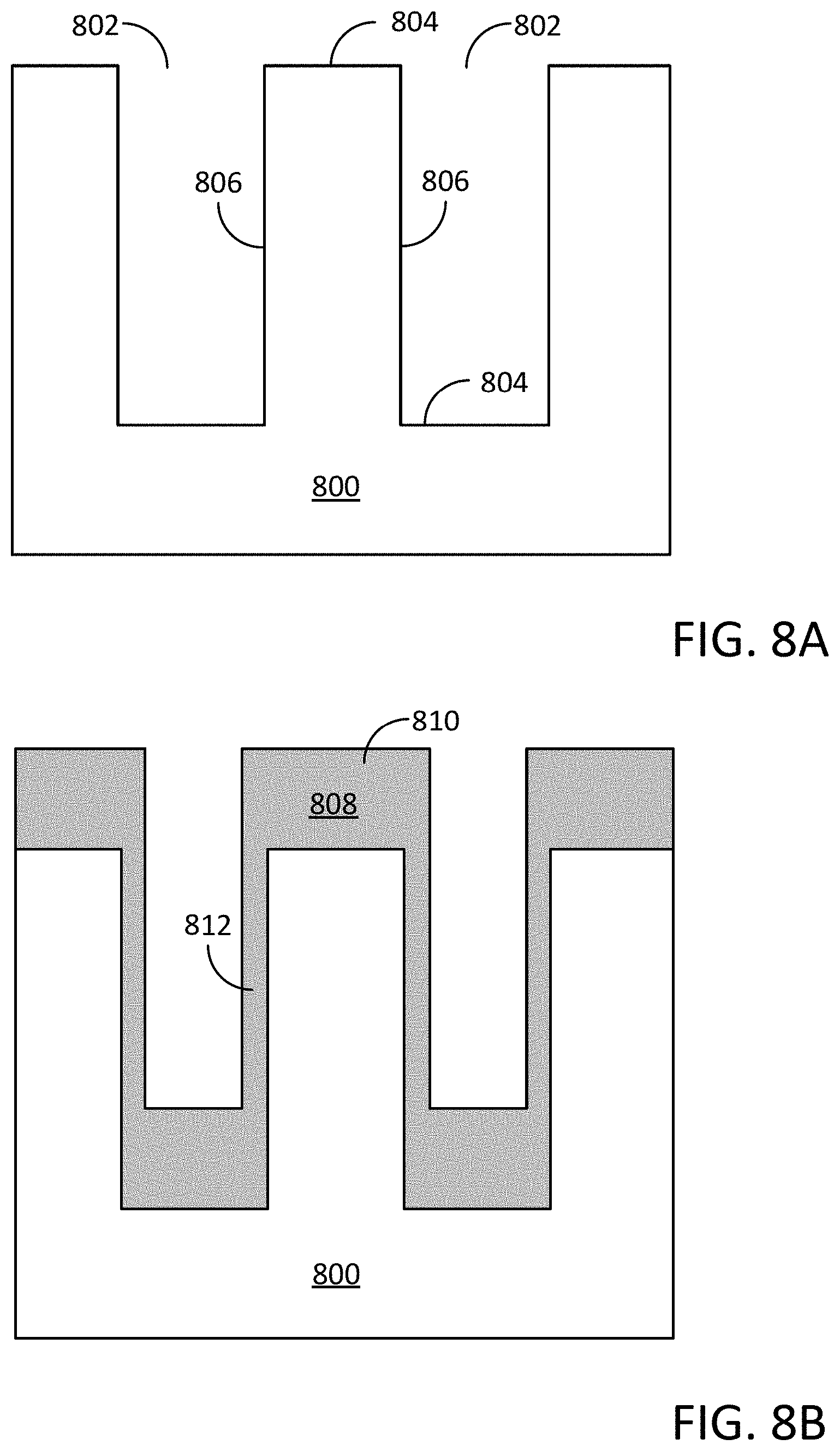
[0020] FIGS. 8A and 8B illustrate an exemplary non-planar substrate prior to and post typographically selective silicon oxide formation, wherein the silicon oxide film is formed selectively over horizontal surfaces of the non-planar substrate relative to vertical surfaces of the non-planar substrate according to the embodiments of the disclosure;
[0021] FIGS. 9A and 9B illustrate scanning tunneling electron microscopy (STEM) images of exemplary non-planar substrates post topographically selective formation of a silicon oxide film wherein the silicon oxide film is selective to deposition over horizontal surfaces relative to vertical surfaces according to the embodiments of the disclosure;
[0022] FIG. 10 illustrates the evolution of both horizontal and vertical silicon oxide film thickness with increasing number of unit deposition cycles of an exemplary topographically selective PEALD process according to the embodiments of the disclosure;
[0023] FIG. 11 illustrates a process flow diagram including an exemplary process for forming a topographically selective silicon oxide film by a PEALD process in accordance with the embodiments of the disclosure;
[0024] FIG. 12 illustrates data representing the etch thickness of an exemplary silicon oxide film in relation to plasma contact time;
[0025] FIG. 13 illustrates an exemplary unit deposition cycle of a PEALD process for forming a topographically selective silicon oxide film according to the embodiments of the disclosure.
[0026] FIG. 14 illustrates a process flow diagram illustrating an exemplary process for forming a topographically selective silicon oxide film by the combination of a cyclical plasma-enhanced deposition and a selective etching according to the embodiments of the disclosure; and
[0027] FIGS. 15A and 15B illustrate an exemplary non-planar substrate after topographically selective deposition of a silicon oxide film with topographical control of the silicon oxide composition and subsequent contact of the silicon oxide film with an etchant to selectively remove the silicon oxide film disposed on horizontal surfaces relative to the silicon oxide film disposed on vertical surfaces according to the embodiments of the disclosure.
[0028] It will be appreciated that elements in the figures are illustrated for simplicity and clarity and have not necessarily been drawn to scale. For example, the dimensions of some of the elements in the figures may be exaggerated relative to other elements to help improve understanding of illustrated embodiments of the present disclosure.
DETAILED DESCRIPTION OF EXEMPLARY EMBODIMENTS
[0029] Although certain embodiments and examples are disclosed below, it will be understood by those in the art that the invention extends beyond the specifically disclosed embodiments and/or uses of the invention and obvious modifications and equivalents thereof. Thus, it is intended that the scope of the invention disclosed should not be limited by the particular disclosed embodiments described below.
[0030] As used herein, the term "topographically selective" may refer to the formation of a film of material on a non-planar substrate with a selectivity to a first plane of the non-planar surface relative to a second plane of the non-planar surface, i.e., the formation of a greater thickness of material on the first plane relative to the thickness of material on the second plane.
[0031] In addition, the "selectivity" of a topographically selective process may be expressed as the ratio of material formed on a first plane of a non-planar substrate relative to the amount of material formed on the first plane and a second plane combined. For example, for a horizontal surface selective process, if a topographically selective process forms 10 nanometers of material on the horizontal surfaces of a non-planar substrate and 1 nanometer of material on the vertical surfaces of the non-planar substrate, the topographical selective process will be considered to have 90% selectivity. As a further example, for a vertical surface selective process, if a topographically selective process forms 10 nanometers of material on the vertical surfaces of a non-planar substrate and 1 nanometer of material on the horizontal surfaces of the non-planar substrate, the topographical selective process will be considered to have 90% selectivity.
[0032] As used herein, the term "substrate" may refer to any underlying material or materials that may be used, or upon which, a device, a circuit, or a film may be formed.
[0033] As used herein, the term "gas" may refer to a vapor or vaporized solid and/or liquid and may be constituted by a single gas or a mixture of gases.
[0034] As used herein, the term "reactive species" may refer to one or more species generated by the plasma excitation of a gas and may include, but is it not limited to, ions, radicals, and excited species.
[0035] As used herein, the term "silicon oxide film" may refer to a film of material comprising at least a silicon component and an oxygen component. In addition to at least the silicon component and the oxygen component, the term "silicon oxide film" may comprise further components, including, but not limited to, a carbon component, a nitrogen component, and a hydrogen component. For example, the silicon oxide film may comprise silicon dioxide (SiO.sub.2), a silicon sub-oxide (SiO.sub.x) wherein x may be less than 2, a silicon oxycarbide, or a doped silicon oxide.
[0036] As used herein, the term "film" and "thin film" may refer to any continuous or non-continuous structures and material deposited by the methods disclosed herein. For example, "film" and "thin film" could include 2D materials, nanolaminates, nanorods, nanotubes, or nanoparticles or even partial or full molecular layers or partial or full atomic layers or clusters of atoms and/or molecules. "Film" and "thin film" may comprise material or a layer with pinholes, but still be at least partially continuous.
[0037] As used herein, the term "cyclical plasma-enhanced deposition process" may refer to a vapor deposition process comprising one or more repeated unit deposition cycles, particularly a plurality of consecutive repetitions of a unit deposition cycle, wherein a unit deposition cycle includes the use of one or more reactive species generated from a plasma.
[0038] As used herein, the term "plasma-enhanced atomic layer deposition" (PEALD) may refer to a vapor deposition process in which deposition cycles, preferably a plurality of consecutive deposition cycles, are conducted in a reaction chamber. Typically, during each unit deposition cycle a precursor is chemisorbed to a deposition surface (e.g., a substrate surface or a previously deposited underlying surface such as material from a previous PEALD cycle), forming a monolayer or sub-monolayer that does not readily react with additional precursor (i.e., a self-limiting reaction). Thereafter, reactive species generated by a plasma produced from one or more precursors may subsequently be introduced into or generated in the reaction chamber for use in converting the chemisorbed precursor to the desired material on the deposition surface. Further, purging steps may also be utilized during each unit deposition cycle to remove excess precursor and reactive species from the reaction chamber and/or remove excess reactant, reactive species and/or reaction byproducts from the reaction chamber after conversion of the chemisorbed precursor.
[0039] As used herein, the term "cyclical plasma-enhanced chemical vapor deposition" (cyclical PECVD) may refer to a vapor deposition process in which deposition cycles, preferably a plurality of consecutive deposition cycles, are conducted in a reaction chamber. Typically, during each unit deposition cycle one or more reactive species may be generated by a plasma through either continuous application of RF power or two or more pulses of RF power. In contrast to PEALD processes, a cyclical PECVD process typically does not employ chemisorption of a vapor phase reactant and subsequent conversion of the chemisorbed molecular layer to the desired material. Cyclical plasma-enhanced chemical vapor deposition may also be referred to as pulsed plasma-enhanced chemical vapor deposition.
[0040] As used herein, the term "horizontal surfaces" may refer to a plane of a substrate which extends essentially horizontally, wherein essentially horizontal may comprise a plane of the substrate within about 30 degrees, or about 15 degrees, or even 5 degrees of horizontal.
[0041] As used herein, the term "vertical surfaces" may refer to a plane of a substrate which extends essentially vertically, wherein essentially vertical may comprise a plane of the substrate within about 30 degrees, or about 15 degrees, or even 5 degrees of vertical.
[0042] A number of example materials are given throughout the embodiments of the current disclosure, it should be noted that the chemical formulas given for each of the example materials should not be construed as limiting and that the non-limiting example materials given should not be limited by a given example stoichiometry.
[0043] In the specification, it will be understood that the term "on" or "over" may be used to describe a relative location relationship. Another element or layer may be directly on the mentioned layer, or another layer (an intermediate layer) or element may be intervened therebetween, or a layer may be disposed on a mentioned layer but not completely cover a surface of the mentioned layer. Therefore, unless the term "directly" is separately used, the term "on" or "over" will be construed to be a relative concept. Similarly to this, it will be understood the term "under", "underlying", or "below" will be construed to be relative concepts.
[0044] The embodiments of the disclosure may include methods for forming a topographically selective silicon oxide film by a cyclical plasma-enhanced deposition process. In particular the topographically selective deposition methods disclosed herein may selectively form a silicon oxide film over a first plane of a non-planar substrate relative to a second plane of a non-planar substrate. For example, a silicon oxide film may be formed selectively over horizontal surfaces of a substrate relative to vertical surfaces of a substrate ("horizontal surface selective process"). Alternatively, a silicon oxide film may be formed selectively over vertical surfaces of a substrate relative to horizontal surfaces of a substrate ("vertical surface selective process").
[0045] The embodiments of the disclosure may provide topographically selective formation processes for forming a silicon oxide film over horizontal surfaces relative to vertical surfaces by a direct topographically selective deposition process. In addition, the embodiments of the disclosure may provide topographically selective formation processes for forming a silicon oxide film over vertical surfaces relative to horizontal surfaces by deposition of a silicon oxide film with topographical control of the silicon oxide film properties such that the deposited silicon oxide film may be contacted with an etchant which may selectively remove the silicon oxide film disposed over horizontal surfaces of the non-planar substrate.
[0046] Next generation semiconductor device processes may desire non-conformal, topographically selective deposition of silicon oxide films. For example, silicon oxide films formed selectively over horizontal surfaces of a substrate, such as, the horizontal surfaces of a trench structure, for example, may be utilized as a sacrificial etch mask due to the etch resistance of the selective silicon oxide film to plasma etching.
[0047] Non-conformal topographically selective film deposition has been demonstrated by a number of methods. For example, a combination of conformal silicon oxide deposition and wet chemical etching has been investigated, wherein the deposition of the silicon oxide film is tuned to obtain a poor quality film over vertical surfaces of the substrate, e.g., over sidewalls of trench structures. In such examples, the vertical silicon oxide film may be selectively removed by an etchant due to the significant higher etch rate of the silicon oxide film on vertical surfaces of the non-planar substrate compared with the silicon oxide film on horizontal surfaces of the non-planar substrate.
[0048] In addition, non-conformal topographically selective film deposition has been demonstrated by utilization of either growth inhibitors or growth accelerators. However, the use of growth inhibitors/accelerators decreases the through-put of processed substrates due to the addition of a chemical wet etching step which is necessary to obtain the desired selectivity. In addition, processing costs may increase due to the expense of inhibitor/accelerator chemical costs as well as the optimization period required to reach the activation/inhibition of the targeted plane.
[0049] The topographically selective formation processes of the current disclosure may be performed within a reaction chamber associated with a PEALD apparatus, or a PECVD apparatus configured with appropriate hardware for pulsing the RF power and sequentially supplying two or more precursors to the reaction chamber. In some embodiments of the disclosure, the reaction chamber utilized for the formation of a topographically selective silicon oxide film may be capable of providing an anisotropic plasma, i.e., a plasma in which at least the ionized species are accelerated in a substantially uniform direction, as opposed to an isotropic plasma in which the excited species traverse in random directions. In some embodiments, the reaction chamber utilized for forming a topographically selective silicon oxide film may generate a plasma, such as a capacitively coupled plasma (CCP) which is excited by applying RF power to one of two electrodes. Further in some embodiments, inductively coupled plasma (ICP), electron cyclotron resonance (ECR) plasma, microwave surface plasma, helicon wave plasma, etc., may be used as the plasma, wherein bias voltage is applied between the electrodes as necessary to increase DC bias between the plasma and electrode.
[0050] As a non-limiting example, the formation of a topographically selective silicon oxide film may enabled by adjusting the bombardment of a plasma excited gas by applying a voltage between two electrodes between which the non-planar substrate is placed in parallel to the two electrodes. A plasma is a partially ionized gas with high free electron content (about 50%), and when a plasma is excited by applying AC voltage between parallel electrodes, ions are accelerated by a self DC bias (VDc) developed between a plasma sheath and the lower electrode. The accelerated ions bombard the non-planar substrate placed on the lower electrode in a direction substantially perpendicular to the horizontal plane of the substrate, i.e., perpendicular to the horizontal plane of the lower electrode (the ion incident direction). The bombardment of a plasma can be represented by plasma density or kinetic energy of ions. The plasma density can be modulated mainly by tuning the pressure within the reaction chamber and the RF power (the lower the pressure and the higher the RF power, the higher the plasma density becomes). The plasma density can also be modulated by applying a DC bias voltage or an AC voltage with a lower frequency set for ions to follow (e.g., less than 1 MHz).
[0051] The cyclical plasma-enhanced deposition processes of the current disclosure may form a topographically selective silicon oxide film by one or more repetitions of a unit deposition cycle, wherein a unit deposition cycle may include the generation of reactive species from a plasma. As a non-limiting example, the deposition cycles may be performed using a suitable apparatus such as the apparatus 100 illustrated in FIG. 1. For example, FIG. 1 is a schematic view of an exemplary PEALD apparatus 100, desirably in conjunction with controls programmed to conduct the sequences described below, usable in some embodiments of the present invention. In this figure, by providing a pair of electrically conductive flat-plate electrodes 104, 102 in parallel and facing each other in the interior 111 (reaction zone) of a reaction chamber 103, applying RF power (e.g., 13.56 MHz, or 27 MHz) 120 to one side, and electrically grounding the other side 112, a plasma is excited between the electrodes. A temperature regulator is provided in a lower stage 102 (the lower electrode), and a temperature of a substrate 101 placed thereon is kept constant at a given temperature. The upper electrode 104 serves as a shower head plate as well, and reactant gas (and noble gas) and precursor gas are introduced into the reaction chamber 103 through a gas line 121 and a gas line 122, respectively, and through the shower head plate 104.
[0052] Additionally, in the reaction chamber 103, a circular duct 113 with an exhaust line 107 is provided, through which gas in the interior 111 of the reaction chamber 103 is exhausted. Additionally, a dilution gas is introduced into the reaction chamber 103 through a gas line 123. Further, a transfer chamber 105 disposed below the reaction chamber 103 is provided with a seal gas line 124 to introduce seal gas into the interior 111 of the reaction chamber 103 via the interior 116 (transfer zone) of the transfer chamber 105 wherein a separation plate 114 for separating the reaction zone and the transfer zone is provided (a gate valve through which a wafer is transferred into or from the transfer chamber 105 is omitted from this figure). The transfer chamber is also provided with an exhaust line 106. In some embodiments, the deposition of multi-element films and surface treatment(s) are performed in the same reaction space, so that all the steps can continuously be conducted without exposing the substrate to air or other oxygen-containing atmosphere. In some embodiments, a remote plasma unit can be used for exciting a gas.
[0053] In some embodiments of the disclosure, a cyclical plasma-enhanced deposition process may be utilized to form a topographically selective silicon oxide film and such processes may include plasma-enhanced atomic layer deposition (PEALD), or cyclical plasma-enhanced chemical vapor deposition (cyclical PECVD). Briefly, a non-planar substrate or a workpiece is placed in a reaction chamber, heated to a deposition temperature, and subjected to alternatively repeated surface reactions, i.e., by one or more repetitions of a unit deposition cycle. In some embodiments, each unit deposition cycle (i.e., PEALD cycle or cyclical PECVD cycle) comprises at least two distinct phases.
[0054] In a first phase, a vapor phase reactant or plasma generated from a vapor phase reactant may be provided into the reaction chamber and contacts the non-planar substrate surface. This reactant or plasma generated reactive species is also referred to herein as the "the silicon precursor", "silicon-containing precursor", "silicon reactant", or "silicon reactive species" and may comprise, for example, a vapor phase reactant or plasma generated from a vapor phase reactant comprising, a silicon component, a carbon component, and a hydrogen component.
[0055] In some embodiments of the disclosure, the silicon reactant consists essentially of a silicon component, a carbon component, and a hydrogen component. In some embodiments, the silicon reactant may comprise an alkylsilane, such as, for example, dimethylsilane, trimethylsilane, tetramethylsilane, diethylsilane, triethylsilane, tetraethylsilane, t-butylsilane (and derivates thereof), or a silicon reactant comprising two silicon atoms, such as hexamethyldisilane, for example. In some embodiments, the silicon reactant may comprise an arylsilane, such as, for example, phenylsilane, diphenylsilane, triphenylsilane, tetraphenylsilane, dibenzylsilane, tribenzylsilane, or tetrabenzylsilane. In some embodiments, the silicon reactant may comprise an aralkylsilane, such as, for example, trimethyl-(3-methylphenyl)silane, or dimethyl(4-methylphenyl)silane.
[0056] In some embodiments of the disclosure, the silicon reactant may further comprise at least one of a nitrogen component or an oxygen component. For example, the silicon reactant may comprise at least one of an alkylalkoxysilane or an alkylaminosilane. In some embodiments, the silicon reactant may comprise an alkylalkoxysilane, such as, for example, methyltrimethoxysilane, ethoxy(trimethyl)silane, diethyl-methyl-ethoxysilane, ethyl(dimethyl)-ethoxysilane, tert-butyl-triethoxysilane, or butyl(trimethoxy)silane. In some embodiments, the silicon reactant may comprise an alkylaminosilane, such as, tris(dimethylamino)ethylsilane, for example.
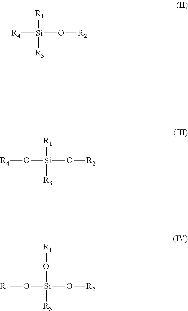
[0057] In some embodiments, the silicon reactant may be represented by the formula (I) below:
##STR00001##
[0058] wherein R.sub.1, R.sub.2, R.sub.3, and R.sub.4 may comprise silicon, carbon, and hydrogen and at least one of R.sub.1, R.sub.2, R.sub.3, and R.sub.4 is different from hydrogen or silicon and R.sub.1, R.sub.2, R.sub.3, and R.sub.4 does not comprise oxygen, nitrogen, or a halogen.
[0059] In some embodiments, the silicon reactant may be represented by the formula (II-IV) below:
##STR00002##
[0060] wherein R.sub.1, R.sub.2, R.sub.3, and R.sub.4 may comprise silicon, carbon, and hydrogen and at least R.sub.3 may be different from hydrogen or silicon and R.sub.1, R.sub.2, R.sub.3, and R.sub.4 does not comprise oxygen, nitrogen, or a halogen.
[0061] In some embodiments, the silicon reactant may be represented by the formula (V-VII) below:
##STR00003##
[0062] wherein R.sub.1, R.sub.2, R.sub.3, and R.sub.4 may comprise silicon, carbon, and hydrogen and at least R.sub.3 may be different from hydrogen or silicon and R.sub.1, R.sub.2, R.sub.3, and R.sub.4 does not comprise oxygen, nitrogen, or a halogen.
[0063] In a second phase, a second reactant comprising a reactive species is provided and may convert the silicon reactant to a silicon oxide film. In some embodiments of the disclosure, the second reactant may comprise a reactive species generated from a plasma produced from a gas comprising an oxygen precursor and a noble gas.
[0064] In some embodiments, the oxygen precursor may comprise at least one of molecular oxygen (O.sub.2), carbon dioxide (CO.sub.2), or nitrous oxide (N.sub.2O). In some embodiments the noble gas comprises at least one of argon, nitrogen, or helium. In some embodiments, the flow rate ratio of the noble gas to the oxygen precursor may be greater than 1, or greater than 2, or even greater than 3.
[0065] Plasmas generated from a gas consisting solely of an oxygen precursor are commonly isotropic comprising primarily oxygen radicals which are not influenced by an electrical field and traverse in substantially random directions. The embodiments of the disclosure generate a plasma from a gas comprising an oxygen precursor and a noble gas such that the generated plasma may be rich in ions which may be influenced by an electric field and particular the plurality of ions may be accelerated anisotropically in a direction downward towards the non-planar substrate in a substantially vertical direction and bombard or impinge the non-planar substrate in a direction substantially perpendicular to a horizontal plane of the substrate, i.e., perpendicular to the horizontal plane of the lower electrode of the deposition apparatus. For example, the ion incident direction may be substantially perpendicular to the lower electrode 102 of apparatus 100 of FIG. 1. In such embodiments of the disclosure, the ion impingement rate, i.e., the rate at which the plurality of ions impact the non-planar substrate, is greater on the horizontal surfaces of the non-planar substrate compared with the vertical surfaces of the non-planar which may result in the topographically selective deposition of a silicon oxide film on the horizontal surfaces of the substrate compared with the vertical surfaces of the substrate. In addition, the difference in ion impingement rate impacting the horizontal surfaces and the vertical surfaces may result in topographic control of the composition of the silicon oxide film, i.e., the composition of the silicon oxide film on horizontal surfaces may be different than the composition of the silicon oxide film on vertical surfaces which may enable a vertical surface selective silicon oxide film by selective etching of the silicon oxide film disposed over horizontal surfaces of the non-planar substrate.
Horizontal Surface Selective Silicon Oxide Formation Processes
[0066] In some embodiments of the disclosure, the methods for forming a topographically selective silicon oxide film by a cyclical plasma-enhanced deposition process may comprise forming a silicon oxide film selectively over horizontal surfaces of a non-planar substrate relative to vertical surfaces of a non-planar substrate, i.e., a greater thickness of the silicon oxide material may be formed over horizontal surfaces of the non-planar substrate relative to the thickness of the silicon oxide material that may be formed over vertical surfaces of the non-planar substrate.
[0067] In some embodiments of the disclosure, the horizontal surface selective silicon oxide formation process may be achieved by the direct deposition of the silicon oxide film selectively on horizontal surfaces relative to vertical surfaces. In some embodiments, the horizontal surface selective silicon oxide deposition process of the current disclosure may comprise a cyclical plasma-enhanced deposition process, such as, for example, a plasma-enhanced atomic layer deposition (PEALD) process, or a cyclical plasma-enhanced chemical vapor deposition (cyclical PECVD) process.
[0068] Therefore, the embodiments of the disclosure may therefore include methods for forming a topographically selective silicon oxide film by a cyclical plasma-enhanced deposition process. The methods may comprise: providing a non-planar substrate including one or more horizontal surfaces and one or vertical surfaces into a reaction chamber; contacting the non-planar substrate with a vapor phase reactant comprising a silicon component, a carbon component, and a hydrogen component; contacting the non-planar substrate with a reactive species generated from a plasma produced from a gas comprising an oxygen precursor and a noble gas; and forming a silicon oxide film either selectively over the horizontal surfaces of the non-planar substrate or selectively over the vertical surfaces of the non-planar substrate.
[0069] The embodiments of the disclosure also include a method for forming a topographically selective silicon oxide film on a non-planar substrate by a plasma-enhanced atomic layer deposition process. The method may comprise: contacting the non-planar substrate with a vapor phase reactant comprising a silicon component, a carbon component, and a hydrogen component; contacting the non-planar substrate with a plurality of ions, including at least oxygen ions, wherein the plurality of ions impinge the substrate in a direction substantially perpendicular to a horizontal plane of the non-planar substrate; and selectively depositing a silicon oxide film over horizontal surfaces of the non-planar substrate relative to vertical surfaces of the non-planar substrate.
[0070] A non-limiting example embodiment of a cyclical plasma-enhanced deposition process that may be utilized to form a horizontally selective silicon oxide film is plasma-enhanced atomic layer deposition (PEALD). Briefly, a substrate or a workpiece is placed in a reaction chamber and subjected to alternatively repeated surface reactions. In some embodiments, the silicon oxide film may be formed by repetition of a self-limiting PEALD cycle.
[0071] An exemplary PEALD process for forming a horizontally selective silicon oxide film is illustrated with reference to FIG. 2. The exemplary PEALD process 200 may comprise two phases, a first phase comprising, contacting the substrate with a vapor phase reactant comprising a silicon component, a carbon component, and a hydrogen component, and a second phase comprising, contacting the substrate with a reactive species generated from a plasma.
[0072] In more detail and with reference to FIG. 2, the exemplary process 200 may commence by means of a process block 210 which comprises, providing a substrate into a reaction chamber and heating the substrate to a suitable deposition temperature.
[0073] In some embodiments, the substrate may comprise one or more materials and material surfaces including, but not limited to semiconductor materials, dielectric materials, and metallic materials. For example, the substrate may include semiconductor materials, such as, but not limited to, silicon (Si), germanium (Ge), germanium tin (GeSn), silicon germanium (SiGe), silicon germanium tin (SiGeSn), silicon carbide (SiC), or a group III-V semiconductor material.
[0074] In some embodiments of the disclosure, the substrate may comprise a patterned non-planar substrate including high aspect ratio features, such as, for example, trench structures, vertical gap features, and/or fin structures. The term "gap feature" may refer to an opening or cavity disposed between opposing inclined sidewalls or two protrusions extending vertically from the surface of the substrate or opposing inclined sidewalls of an indentation extending vertically into the surface of the substrate, such a gap feature may be referred to as a "vertical gap feature" comprising both horizontal surfaces and vertical surfaces. In some embodiments, the vertical gap features may have an aspect ratio (height:width) which may be greater than 2:1, or greater than 5:1, or greater than 10:1, or greater than 25:1, or greater than 50:1, or even greater than 100:1, wherein "greater than" as used in this example refers to a greater distance in the height of the gap feature.
[0075] In some embodiments, the substrate on which deposition is desired is loaded into a reaction chamber. In some embodiments, the reaction chamber may form a part of a cluster tool in which a variety of different processes in the formation of semiconductor device structures are carried out. In some embodiments, a flow-type reactor may be utilized. In some embodiments, a showerhead-type reactor may be utilized. In some embodiments, a space divided reactor may be utilized. In some embodiments, a high-volume manufacturing-capable single wafer PEALD reactor may be utilized. In other embodiments, a batch reactor comprising multiple substrates may be utilized. For embodiments in which a batch PEALD reactor is used, the number of substrates may be in the range of 10 to 200, or 50 to 150, or even 100 to 130.
[0076] In some embodiments, if necessary, the exposed surfaces of the substrate may be pretreated to provide reactive sites to react with the first phase of the PEALD process. In some embodiments, a separate pretreatment step is not required. In some embodiments, the substrate is pretreated to provide a desired surface termination, for example, by exposing the substrate surface to a pretreatment plasma.
[0077] In some embodiments of the disclosure, the substrate disposed within the reaction chamber may be heated to a desired deposition temperature for a subsequent cyclical deposition stage 205 of exemplary PEALD process 200 (FIG. 2). For example, the substrate may be heated to a substrate deposition temperature of less than approximately 600.degree. C., or less than approximately 550.degree. C., or less than approximately 500.degree. C., or less than approximately 450.degree. C., or less than approximately 400.degree. C., or less than approximately 350.degree. C., or less than approximately 300.degree. C., or even less than approximately 250.degree. C. In some embodiments of the disclosure, the substrate deposition temperature during the exemplary plasma enhanced atomic layer deposition process 200 may be between approximately 150.degree. C. and approximately 600.degree. C.
[0078] In addition to controlling the temperature of the substrate, the pressure in the reaction chamber may also be regulated to enable deposition of a desired silicon oxide film. In some embodiments, regulating the pressure within the reaction chamber may also control the population density and the nature of the reactive species generated within the plasma. Therefore, in some embodiments, the pressure in the reaction chamber during the exemplary PEALD process 200 may be regulated at a pressure greater than 150 Pascals, or greater than 300 Pascals, or greater than 450 Pascals, or greater than 600 Pascals, or even greater than 800 Pascals. For example, in some embodiments, the pressure within the reaction chamber during the exemplary PEALD process 200 may be regulated between 150 Pascals and 800 Pascals.
[0079] Once the temperature of substrate has been set to the desired deposition temperature and pressure in the reaction chamber has been regulated as desired, the exemplary process 200 may continue by means of a cyclical deposition stage 205 which may include providing one or more deposition gases to the reaction chamber, wherein deposition gases may include vapor phase reactants, purge gas, carrier gas, and a gas utilized to generate a reactive species from a plasma.
[0080] In brief, in a first phase of the cyclical deposition stage 205, a vapor phase reactant comprising a silicon component, a carbon component, and a hydrogen component "the silicon precursor" may be "pulsed" into the reaction chamber, wherein the term "pulse" may be understood to comprise feeding a reactant into the reaction chamber for a predetermined amount of time. The term "pulse" does not restrict the length or duration of the pulse and a pulse may be any length of time. In some embodiments, in addition to a silicon precursor a gas mixture may be provided to the reaction chamber continuously during the cyclical deposition stage 205 of exemplary PEALD process 200. In some embodiments, the gas mixture may comprise both a gas mixture for generation of reactive species utilized during the second stage of the PEALD process 200 and may also be utilized as a purge gas to remove excess reactants, reactive species, and reaction byproducts from the reaction chamber.
[0081] In more detail, the cyclical deposition stage 205 of exemplary PEALD process 200 may continue by means of a process block 220 comprising, contacting the substrate with a vapor phase reactant comprising a silicon component, a carbon component, and a hydrogen component, i.e., the silicon precursor.
[0082] In some embodiments, the silicon precursor may be provided first to the substrate. After an initial surface termination, if necessary or desired, a silicon precursor pulse may be supplied to the substrate. In accordance with some embodiments, the silicon precursor may be supplied to the reaction chamber along with a carrier gas flow. In some embodiments, the silicon precursor may comprise a volatile silicon species that is reactive with the surface(s) of the substrate. The silicon precursor pulse may self-saturate the substrate surfaces such that excess constituents of the silicon precursor pulse do not further react with the molecular layer formed by this process.
[0083] The silicon precursor pulse is preferably supplied as a vapor phase reactant. The silicon precursor gas may be considered "volatile" for the purposes of the present disclosure if the species exhibits sufficient vapor pressure under the process conditions to transport species to the substrate surface in sufficient concentration to saturate the exposed surfaces.
[0084] In some embodiments of the disclosure, the vapor phase reactant consists essentially of a silicon component, a carbon component, and a hydrogen component. In some embodiments, the vapor phase reactant may comprise an alkylsilane, an arylsilane, an aralkylsilane, an alkylalkoxysilane, or an alkylaminosilane, as described previously herein.
[0085] In some embodiments of the disclosure, the silicon precursor may be pulsed into the reaction chamber for a time period from about 0.05 second to about 5.0 seconds, or from about 0.1 seconds to about 3 seconds, or even from about 0.2 seconds to about 1.0 seconds. In some embodiments, the silicon precursor may be pulsed into the reaction chamber for a time period of less than 0.1 seconds, or even less than 0.05 seconds. In addition, during the contacting of the substrate with the silicon precursor, the flow rate of the silicon precursor may be less than 1000 sccm, or less than 500 sccm, or less than 100 sccm, or less than 50 sccm, or even less than 5 sccm. In addition, during the contacting of substrate with the silicon precursor the flow rate of the silicon precursor may range from about 5 to 50 sccm, or from about 50 to 100 sccm, or from about 100 to about 1000 sccm.
[0086] After sufficient time for a molecular layer to adsorb on the substrate surface, excess silicon precursor may be removed from the reaction chamber. In some embodiments, the excess silicon precursor may be purged by stopping the flow of the vapor phase silicon precursor while continuing to flow a carrier gas, a purge gas, or a gas mixture, for a sufficient time to diffuse or purge excess reactants and reactant by-products, if any, from the reaction chamber. In some embodiments, the excess silicon precursor may be purged with the aid of one or more inert gases, such as nitrogen, helium, or argon that may be flowing throughout the cyclical deposition phase 205 of exemplary PEALD process 200.
[0087] In some embodiments, the silicon precursor may be purged from the reaction chamber for a time period of about 0.1 seconds to about 60 seconds, or about 0.3 seconds to about 30 seconds, or even about 0.3 seconds to about 10 second. Provision and removal of the silicon precursor may be considered as the first or "silicon phase" of the exemplary PEALD process 200.
[0088] Upon completion of the purging of the reaction chamber of excess silicon precursor and any reaction by-products, the cyclical deposition stage 205 of exemplary PEALD process 200 may continue with a second phase by means of a process block 230 comprising, contacting the substrate with a reactive species generated from a plasma produced from a gas comprising an oxygen precursor and a noble gas.
[0089] In some embodiments, the oxygen precursor may comprise at least one of molecular oxygen (O.sub.2), carbon dioxide (CO.sub.2), or nitrous oxide (N.sub.2O). In some embodiments the noble gas comprises at least one of argon, nitrogen, or helium. In some embodiments, the flow rate ratio of the noble gas to the oxygen precursor into the reaction chamber may be greater than 1, or greater than 2, or even greater than 3. As previously described, the plasma ("the oxygen based plasma") may be rich in ions, including at least oxygen ions, and may be generated using a parallel plate electrode configuration which may accelerate anisotropically a plurality of ions downward towards the substrate in a substantially vertical direction.
[0090] In some embodiments, an oxygen based plasma may be generated by applying RF power from about 50 W to about 1000 W, or from about 100 W to about 500 W, or from about 100 W to about 300 W. In some embodiments, the plasma may be generated in-situ, while in other embodiments the plasma may be generated remotely. In some embodiments, a showerhead reactor may be utilized and plasma may be generated between a lower electrode (i.e., a susceptor on top of which the substrate is located) and an upper electrode (i.e., a showerhead plate).
[0091] In some embodiments, the reactive species generated from the plasma may contact the substrate for a time period between about 0.1 seconds to about 12 seconds, or about 0.5 seconds to about 5.0 seconds, or even about 0.5 seconds to about 2.0 seconds. In some embodiments, the reactive species generated from the plasma may contact the substrate for a time period of less than 1 second, or less than 0.5 seconds, or even less than 0.1 seconds.
[0092] After a time period sufficient to completely saturate and react the previously absorbed molecular layer with the oxygen based plasma pulse, any excess reactant and reaction byproducts may be removed from the reaction chamber. As with the removal of the vapor phase reactant, i.e. the silicon precursor, this step may comprise stopping generation of reactive species and continuing to flow an inert gas. The inert gas flow may flow for a time period sufficient for excess reactive species and volatile reaction byproducts to diffuse out of and be purged from the reaction chamber. For example, the purge process may be utilized for a time period between about 0.1 seconds to about 10 seconds, or about 0.1 seconds to about 4.0 seconds, or even about 0.1 seconds to about 0.5 seconds. Together, the oxygen based plasma provision and removal represent a second, reactive species phase in the exemplary silicon nitride PEALD process 200 of FIG. 2.
[0093] The method wherein the substrate is alternately and sequentially contacted with the vapor phase silicon precursor and contacted with the reactive species generated from a gas comprising an oxygen precursor and a noble gas may constitute a unit deposition cycle. In some embodiments of the disclosure, the exemplary PEALD process 200 may comprise repeating the unit deposition cycle one or more times. For example, the cyclical deposition stage 205 of exemplary PEALD process 200 may continue with a decision gate 240 which determines if the PEALD process 200 continues or exits. The decision gate of process block 240 is determined based on the thickness of the silicon oxide film deposited, for example, if the thickness of the silicon oxide film is insufficient for the desired device structure, then the PEALD process 200 may return to the process block 220 and the processes of contacting the substrate with the silicon precursor (process block 220) and contacting the substrate with the reactive species (process block 230) may be repeated one or more times. Once the silicon oxide film has been deposited to a desired thickness the exemplary PEALD process 200 may exit by means of a process block 250 and the silicon oxide film may be subjected to additional processes to form a semiconductor device structure.
[0094] While the PEALD cycle is generally referred to herein as beginning with the silicon phase, it is contemplated that in other embodiments the cycle may begin with the reactive species phase. One of skill in the art will recognize that the first precursor phase generally reacts with the termination left by the last phase in the previous cycle. Thus, while no reactant may be previously absorbed on the substrate surface or present in the reaction chamber if the reactive species is the first phase in the PEALD cycle, in subsequent cycles the reactive species phase will effectively follow the silicon phase. In some embodiments, one or more different PEALD cycles are provided in the deposition process.
[0095] A further overview of a non-limiting exemplary unit deposition cycle of the horizontally selective PEALD processes of the current disclosure is illustrated with reference to FIG. 3. As illustrated in FIG. 3, the horizontal axis represents the time parameter but does not necessarily represent the actual time length of individual processes, and the vertical axis represents an ON-state or OFF-state for gas flow and RF power, wherein a raised level on the vertical axis of each parameter represents an ON-state but the vertical axis of each line does not necessarily represent the actual quantity of the associated parameter, whereas a bottom level of each line on the vertical axis represents an OFF-state, i.e., zero gas flow, or no RF power supplied.
[0096] In brief, in a first period 310 (i.e., the precursor pulse period) of the unit deposition cycle the silicon precursor may be pulsed into the reaction chamber along with a flow of noble gas and the oxygen precursor. In this first period 310, the silicon precursor may chemisorb on the non-planar surface of the substrate forming at most a monolayer. In a second period 320 (i.e., a purge period) the flow of silicon precursor is stopped and the flow of the noble gas and the oxygen precursor continues such that the reaction chamber is purged of excess silicon precursor any reaction by-products. In a third period 330 (i.e., the RF pulse period) the oxygen precursor and noble gas flow continues into the reaction chamber and a pulse of RF power is supplied to the gas to excite a plasma and generate reactive species which may react with the chemisorbed silicon precursor thereby forming a silicon oxide film. In a fourth period 340 (i.e., a purge period) the RF power is in the OFF-state and noble gas and oxygen precursor flow continues thereby purging the reaction chamber of excess reactive species and any reaction by-products.
[0097] A further non-limiting example embodiment of a cyclical plasma-enhanced deposition process that may be utilized to form a horizontally selective silicon oxide film is cyclical plasma-enhanced chemical vapor deposition (cyclical PECVD). Briefly, a non-planar substrate or workpiece may be placed in a reaction chamber and subjected to one or more cyclical PECVD deposition cycles.
[0098] An exemplary cyclical PECVD process for forming a horizontally selective silicon oxide film is illustrated with reference to FIG. 4. The exemplary cyclical PECVD process 400 may comprise two phases, a first phase comprising contacting the substrate with a first reactive species generated from a vapor phase reactant comprising a silicon component, a carbon component, and a hydrogen component, and a second phase comprising contacting the substrate with a second reactive species generated from a gas comprising an oxygen precursor and a noble gas.
[0099] In more detail and with reference to FIG. 4, the exemplary process 400 may commence by means of a process block 410 which comprises, providing a substrate into a reaction chamber and heating the substrate to a suitable deposition temperature.
[0100] In some embodiments of the disclosure, the substrate may comprise the materials and topography as previously disclosed herein and particularly comprises a non-planar substrate including one or more horizontal surfaces and one or more vertical surfaces. In addition, the reaction chamber may comprise any of the reaction chambers (and associated apparatus) as described previously herein and particularly may comprise a plasma-enhanced chemical vapor deposition (PECVD) reaction chamber and associated apparatus including a parallel plate electrode configuration for generating an anisotropic plasma.
[0101] In some embodiments of the disclosure, the substrate disposed within the reaction chamber may be heated to a desired deposition temperature for a subsequent cyclical deposition stage 405 of exemplary cyclical PECVD process 400 (FIG. 4). For example, the substrate may be heated to a substrate temperature of less than approximately 600.degree. C., or less than approximately 550.degree. C., or less than approximately 500.degree. C., or less than approximately 450.degree. C., or less than approximately 400.degree. C., or less than approximately 350.degree. C., or less than approximately 300.degree. C., or even less than approximately 250.degree. C. In some embodiments of the disclosure, the substrate temperature during the exemplary cyclical PECVD process 300 may be between approximately 150.degree. C. and approximately 600.degree. C.
[0102] In addition to controlling the temperature of the substrate, the pressure in the reaction chamber may also be regulated to enable deposition of a desired silicon oxide film. In some embodiments, regulating the pressure within the reaction chamber may also control the population density and the nature of the reactive species generated within the plasma. Therefore, in some embodiments, the pressure in the reaction chamber during the exemplary cyclical PECVD process 400 may be regulated at a pressure greater than 150 Pascals, or greater than 300 Pascals, or greater than 450 Pascals, or greater than 600 Pascals, or even greater than 800 Pascals. For example, in some embodiments, the pressure within the reaction chamber during the exemplary cyclical PECVD process 400 may be regulated between 150 Pascals and 800 Pascals.
[0103] Once the temperature of substrate has been set to the desired deposition temperature and pressure in the reaction chamber has been regulated as desired, the exemplary process 400 may continue by means of a cyclical deposition stage 405 which may include contacting the substrate with a first reactive species generated from a plasma and contacting the substrate with a second reactive species generated from a plasma.
[0104] In more detail, the cyclical deposition stage 405 of exemplary cyclical PECVD process 400 may continue by means of a process block 420 comprising, contacting the substrate with a first reactive species generated from a vapor phase reactant comprising a silicon component, a carbon component, and a hydrogen component, i.e., the silicon precursor.
[0105] In some embodiments, the first reactive species may comprise multiple reactive species generated at least from a vapor phase reactant comprising a silicon component, a carbon component, and a hydrogen component. For example, the vapor phase reactant may comprise all the silicon precursors previously disclosed herein and may include, but is not limited to, an alkylsilane, an arylsilane, an aralkylsilane, an alkylalkoxysilane, or an alkylaminosilane.
[0106] In some embodiments of the disclosure, the first reactive species may contact the non-planar substrate for a time period from about 0.05 second to about 5.0 seconds, or from about 0.1 seconds to about 3 seconds, or even about 0.2 seconds to about 1.0 seconds. In addition, during the contacting of the substrate with the first reactive species, the flow rate of vapor phase reactant may be less than 1000 sccm, or less than 500 sccm, or less than 100 sccm, or less than 50 sccm, or even less than 5 sccm.
[0107] The cyclical deposition stage 405 of exemplary cyclical PECVD process 400 may continue by means of a process block 430 comprising, contacting the substrate with a second reactive species generated from a gas comprising an oxygen precursor and a noble gas. In some embodiments, the oxygen precursor may comprise at least one of molecular oxygen (O.sub.2), carbon dioxide (CO.sub.2), or nitrous oxide (N.sub.2O), and the noble gas may comprise at least one of argon, nitrogen, or helium.
[0108] In some embodiments, the second reactive species may be generated from a plasma and may contact the substrate for a time period between about 0.1 seconds to about 12 seconds, or about 0.5 seconds to about 5.0 seconds, or even about 0.5 seconds to about 2.0 seconds. In some embodiments, the second reactive species generated from the plasma may contact the substrate for a time period of less than 1 second, or less than 0.5 seconds, or even less than 0.1 seconds.
[0109] The method wherein the substrate is contacted with a first reactive species and contacted with a second reactive species may constitute a unit deposition cycle. In some embodiments of the disclosure, the exemplary cyclical PECVD process 400 may comprise repeating the unit deposition cycle one or more times. For example, the cyclical deposition stage 405 of exemplary cyclical PECVD process 400 may continue with a decision gate 440 which determines if the cyclical PECVD process 400 continues or exits. The decision gate of process block 440 is determined based on the thickness of the silicon oxide film deposited, for example, if the thickness of the silicon oxide film is insufficient for the desired device structure, then the cyclical PECVD process 400 may return to the process block 420 and the processes of contacting the substrate with the first reactive species (process block 420) and contacting the substrate with the second reactive species (process block 430) may be repeated one or more times. Once the silicon oxide film has been deposited to a desired thickness the exemplary cyclical PECVD process 400 may exit by means of a process block 450 and the silicon oxide film may be subjected to additional processes to form a semiconductor device structure.
[0110] While the exemplary cyclical PECVD process 400 of FIG. 4 is illustrated as first contacting the substrate with the first reactive species and subsequently contacting the substrate with the second reactive species, it should be appreciated that all alternative sequences of contacting the substrate with reactive species may be utilized in the cyclical PECVD processes of the current disclosure. For example, in some embodiments, both the first reactive species and the second reactive species may contact the substrate simultaneously within a unit deposition cycle. As a further example, in some embodiments, the second reactive species may contact the substrate subsequently followed by contacting the substrate with the first reactive species within a unit deposition cycle. In some embodiments, the substrate may be repeatedly contacted with the first reactive species prior to subsequently contacting the substrate with the second reactive species one or more times within a unit deposition cycle. Alternatively, the substrate may be repeatedly contacted with the second reactive species prior to subsequently contacting the substrate with the first reactive species one or more times within a unit deposition cycle. In some embodiments, a purge cycle may follow the contacting of the substrate with a reactive species, as previously described herein.
[0111] A further overview of a non-limiting exemplary unit deposition cycle of the horizontally selective cyclical PECVD processes of the current disclosure is illustrated with reference to FIG. 5. As illustrated in FIG. 5, the horizontal axis represents the time parameter and the vertical axis represents an ON-state or OFF-state, as previously described with reference to FIG. 3.
[0112] In brief, in a first period 510 (i.e., the deposition period) of the unit deposition cycle the noble gas and oxygen precursor may flow into reaction chamber, along with a pulse of the silicon precursor while applying a continuous feed of RF power. In the second 520, third 530, and fourth 540 periods (i.e., the purge periods) the flow of silicon precursor may be in the OFF-state while the flow of noble gas and oxygen precursor is maintained along with the continuous feed of RF power.
[0113] Therefore, in some embodiments, a unit deposition cycle comprises, simultaneously contacting the substrate with the first reactive species and the second reactive species, and purging excess first reactive species and second reactive species and any reaction by-products. In such embodiments, the first reactive species and the second reactive species may contact the non-planar substrate for a time period of less than 1 second, or less than 0.5 seconds, or less than 0.1 seconds. In some embodiments, a short period of contact between the non-planar substrate and the first and second reactive species may result in the deposition of a silicon oxide film which is topographically selective to the upper horizontal surfaces of the non-planar substrate, e.g., more material is deposited on the upper horizontal surfaces of a trench structure when compared with the material deposited on the lower horizontal surfaces, i.e., at the bottom surface of the trench structure and vertical surfaces, i.e., trench sidewalls.
[0114] An additional exemplary unit deposition cycle of the exemplary horizontally selective cyclical PECVD processes of the current disclosure is illustrated with reference to FIG. 6. As illustrated in FIG. 6, the horizontal axis represents the time parameter and the vertical axis represents an ON-state or OFF-state, as previously described with reference to FIG. 3.
[0115] In brief, in a first period 610 (i.e., the deposition period) of the unit deposition cycle noble gas may flow into the reaction chamber, along with a pulse of the oxygen precursor. In addition, in the first period 610, the silicon precursor may be introduced into the reaction chamber by two or more discrete pulses and RF power may be applied as a discrete pulse. In a second period 620 (i.e., the purge period) of the unit deposition cycle, oxygen precursor flow, silicon precursor flow, and RF power may be in the OFF-state whilst a flow of noble gas is maintained into the reaction chamber to thereby purge the reaction chamber. In a third period 630 (i.e., the treatment period) of the unit deposition cycle the flow of noble gas may be increased, i.e., ramped, for a selected time period and a discrete pulse of RF power may be applied to the noble gas thereby generating excited species of the noble gas. In some embodiments, the excited species of the noble gas, e.g., argon ions or helium ions, may be employed to remove excess silicon oxide film deposition disposed at the edge of horizontal surfaces of the non-planar substrate. In the fourth period 640 (i.e., a purge period), the flow of noble gas may be ramped down to the previous flow level while the oxygen precursor flow, silicon precursor flow, and RF power are in the OFF-state.
[0116] Therefore, in some embodiments, a unit deposition cycle may comprise, simultaneously contacting the substrate with the first reactive species and the second reactive species, purging excess first reactive species and excess second reactive species and any reaction by-products, contacting the substrate with a third reactive species generated from a noble gas, i.e., plasma excitation of the noble gas, and purging excess third reactive species and any reaction by-products from the reaction chamber. In such embodiments, the silicon oxide film may be deposited selectively over the horizontal surfaces of the non-planar substrate relative to the vertical surfaces of the non-planar substrate.
[0117] An additional exemplary unit deposition cycle of the exemplary horizontally selective cyclical PECVD processes of the current disclosure is illustrated with reference to FIG. 7. As illustrated in FIG. 7, the horizontal axis represents the time parameter and the vertical axis represents an ON-state or OFF-state, as previously described with reference to FIG. 3.
[0118] In brief, in a first period 710 (i.e., the deposition period) of the unit deposition cycle noble gas may flow noble gas into reaction chamber, along with two or more pulses of the silicon precursor. In addition, during the first period 710 a discrete pulse of RF power may be applied to the gas. In such embodiments, a film comprising silicon, carbon, and hydrogen may be deposited by a sputtering effect on the horizontal surfaces of the substrate. In a second period 720 (i.e., a purge period) noble gas flow may be maintained, and silicon precursor flow and RF power may be in the OFF-state. In a third period 730 (i.e., the oxidation period) noble gas flow may be maintained while an oxygen precursor pulse is supplied into the reaction chamber along with a discrete pulse of RF power. In some embodiments, the third period 730 may produce an oxygen based plasma which may oxidize the previously sputter deposited film thereby forming a silicon oxide film. In the fourth period 740 (i.e., a purge period), the flow of noble gas may be maintained while the oxygen precursor flow, silicon precursor flow, and RF power are in the OFF-state.
[0119] Therefore, in some embodiments, a unit deposition cycle may comprise, contacting the substrate with the first reactive species, contacting the substrate with a fourth reactive species generated from a gas comprising a noble gas, purging any reactive species and reaction by-products from the reaction chamber, contacting the substrate with the second reactive species, and purging any reactive species and reaction by-products from the reaction chamber. In such embodiments, the silicon oxide film may be deposited selectively over the horizontal surfaces of the non-planar substrate relative to the vertical surfaces of the non-planar substrate.
[0120] As a non-limiting example of the embodiments of the disclosure FIGS. 8A-B illustrate schematic cross-sectional diagrams of an exemplary non-planar substrate prior to topographically selective silicon oxide formation (FIG. 8A) and post typographically selective silicon oxide formation (FIG. 8B), wherein the silicon oxide film is formed selectively over horizontal surfaces of the non-planar substrate relative to vertical surfaces of the non-planar substrate.
[0121] In more detail, FIG. 8A illustrates a schematic cross sectional diagram of a non-planar substrate 800. The non-planar substrate may comprise all the materials and topographies as previous described herein, and in particular embodiments the non-planar substrate 800 may comprise a silicon substrate. The non-planar substrate 800 may include a number of trench structures 802 ("vertical gap features") which may comprise one or more horizontal surfaces 804 and one or more vertical surfaces 806.
[0122] FIG. 8B illustrates a schematic cross sectional diagram of the non-planar substrate 800 after forming a topographically selective silicon oxide over the horizontal surfaces and the vertical surfaces. As illustrated in FIG. 8B a silicon oxide film 808 may be deposited over the non-planar substrate 800 utilizing either the PEALD processes or cyclical PECVD processes described above. In this particular example, the silicon oxide is formed by a horizontal surface selective process and therefore the silicon oxide film 808 may comprise a silicon oxide film 810 disposed over the horizontal surfaces of the non-planar substrate 800 with a greater thickness than the silicon oxide film 812 disposed over the vertical surfaces of the non-planar substrate 800.
[0123] As previously disclosed herein, the "selectivity" of a topographically selective process may be expressed as the percent ratio of material formed on a first plane of a non-planar substrate relative to the amount of material formed on the first plane and a second plane combined. For this example of a horizontal surface selective process, the selectivity may be calculated as a percentage ratio of the thickness of the silicon oxide film disposed over the horizontal surfaces compared with the combined thickness of the silicon oxide film disposed over both the horizontal surfaces and the vertical surfaces. Therefore in some embodiments of the disclosure, the topographical selectivity may be greater than 50%, or greater than 60%, or greater than 70%, or greater than 80%, or greater than 90%, or even equal to 100%, for deposition over the horizontal surfaces of the non-planar substrate compared with deposition over the vertical surfaces of the non-planar substrate.
[0124] As further non-limiting examples of the embodiments of the disclosure, FIGS. 9A-B illustrate scanning tunneling electron microscopy (STEM) images of exemplary non-planar substrates post topographically selective formation of a silicon oxide film wherein the silicon oxide film is selective to deposition over horizontal surfaces relative to vertical surfaces.
[0125] In more detail, the non-planar topographically selective silicon oxide films of FIGS. 9A-B were deposited by a PEALD process utilizing hexamethyldisilane as the silicon precursor, molecular oxygen (O.sub.2) as the oxygen precursor, and argon as the noble gas, at a deposition temperature of approximately 250.degree. C.
[0126] FIG. 9A illustrates a non-planar silicon substrate 900 and a silicon oxide film disposed over the horizontal surface of the non-planar substrate 902 and a silicon oxide film disposed over vertical surfaces of the non-planar substrate 904. In this non-limiting example, the unit deposition cycle of the PEALD process was repeated for 500 cycles to obtain the thickness of silicon oxide film illustrated in FIG. 9A. Examination of FIG. 9A illustrates that the silicon oxide film disposed over the horizontal surface 902 has a thickness of approximately 7 nanometers and the silicon oxide film disposed over the vertical surfaces 904 has a thickness of approximately 3 nanometers, resulting in a horizontal surface selective process with a selectivity of 70%.
[0127] FIG. 9B illustrates a further non-planar silicon substrate 906 and a silicon oxide film disposed over the horizontal surface of the non-planar substrate 908 and a silicon oxide film disposed over vertical surfaces of the non-planar substrate 910. In this non-limiting example, the unit deposition cycle of the PEALD process was repeated for 1000 cycles to obtain the thickness of silicon oxide film illustrated in FIG. 9B. Examination of FIG. 9B illustrates that the silicon oxide film disposed over the horizontal surface 908 has a thickness of approximately 11 nanometers and the silicon oxide film disposed over the vertical surfaces 910 has a thickness of approximately 3.5 nanometers, resulting in a horizontal surface selective process with a selectivity of 75%.
[0128] As further non-limiting examples of the embodiments of the invention FIG. 10 illustrates the evolution of both horizontal and vertical silicon oxide film thickness with increasing number of unit deposition cycles for an exemplary topographically selective PEALD. In more detail, the topographically selective PEALD process of this example is a horizontal surface selective process, i.e., a greater thickness of the silicon oxide film is deposited over the horizontal surfaces compared with the thickness of the silicon oxide film deposited over the vertical surfaces. In this exemplary PEALD process, the silicon precursor is hexamethyldisilane, the oxygen precursor is molecular oxygen (O.sub.2), and the noble gas is argon, and the deposition temperature is approximately 250.degree. C. Further examination of FIG. 10 illustrates that the silicon oxide film disposed over horizontal surfaces is considerably thicker than the silicon oxide film disposed over vertical surfaces. For example, the silicon oxide film deposited after 500 deposition cycles has a horizontal thickness of approximately 7 nanometers and a vertical thickness of approximately 3 nanometers resulting in a selectivity of 70%. As a further example, the silicon oxide film deposited after 1000 deposition cycles has horizontal thickness of approximately 11 nanometers and a vertical thickness of 3.5 nanometers resulting a in a selectivity of 75%.
Vertical Surface Selective Silicon Oxide Formation Processes
[0129] In some embodiments of the disclosure, methods for forming a topographically selective silicon oxide film by a cyclical plasma-enhanced deposition process may comprise forming a silicon oxide film selectively over vertical surfaces of a non-planar substrate relative to horizontal surfaces of a non-planar substrate, i.e., a greater thickness of the silicon oxide material may be formed over vertical surfaces of the non-planar substrate relative to the thickness of the silicon oxide material that may be formed over horizontal surfaces of the non-planar substrate.
[0130] In some embodiments of the disclosure, the vertically selective silicon oxide formation process may be achieved utilizing the topographically selective deposition methods previously disclosed in conjunction with selective etching of the silicon oxide film disposed over horizontal surfaces.
[0131] In some embodiments, a vertical surface selective process may be achieved by forming a topographically selective silicon oxide film by a cyclical plasma-enhanced deposition, such as, for example, plasma-enhanced atomic layer deposition (PEALD), or cyclical plasma-enhanced chemical vapor deposition (cyclical PECVD). In some embodiments, the cyclical plasma-enhanced deposition may include a cyclical etch of the silicon oxide film disposed over horizontal surfaces of the non-planar substrate. In some embodiments, the silicon oxide film may be contacted with an etchant post deposition.
[0132] In some embodiments, the selective formation of a silicon oxide film on the vertical surfaces of a non-planar substrate comprises, depositing a silicon oxide film with a higher carbon content on the vertical surfaces of a non-planar substrate compared with the carbon content of the silicon oxide film on the horizontal surfaces of a non-planar substrate, i.e., topographical composition control over the silicon oxide film deposition. The topographical composition control over the silicon oxide film deposition may be enabled by utilizing a silicon precursor comprising a silicon component, a carbon component, and a hydrogen component, in addition to utilizing an anisotropic oxygen based plasma produced from a gas comprising an oxygen precursor and a noble gas.
[0133] As a non-limiting example of topographical composition control of the silicon oxide film deposition, a unit deposition cycle of cyclical plasma-enhanced deposition process may comprise chemisorbing the silicon precursor over the non-planar surface forming at most a monolayer of the silicon precursor, and subsequently contacting the non-planar substrate with an anistropic plasma comprising a plurality of ions which are accelerated downward toward the substrate in a substantially vertical direction. Due to the ion incident direction being substantially perpendicular to the horizontal plane of the non-planar substrate a greater number of ions bombard or impinge the horizontal surfaces of the non-planar substrate relative to the vertical surfaces. Therefore, reaction of ions with the adsorbed silicon species will be greater on horizontal surfaces compared with vertical surfaces, thereby full transformation of the deposited film on the vertical surfaces may not be achieved resulting in a significant carbon content being retained in the silicon oxide film disposed over the vertical surfaces.
[0134] Therefore, in some embodiments, a topographically selective deposition process may deposit a silicon oxide film on the vertical surfaces of the non-planar substrate comprising a higher carbon content than the silicon oxide film on the horizontal surfaces of the non-planar substrate. For example, the silicon oxide film disposed over the vertical surfaces may comprise a silicon oxycarbide, or a carbon doped silicon oxide. The etch rate of the deposited silicon oxide film may be different depending on the concentration of carbon in the deposited silicon oxide film. For example, in some embodiments, the silicon oxide film on the vertical surfaces of the non-planar substrate may have a lower etch rate than the silicon oxide film on the horizontal surfaces of the non-planar substrate.
[0135] The difference in etch rate of the deposited silicon oxide film due to the topographical composition control may be exploited to selectively remove the silicon oxide film disposed over the horizontal surfaces relative to the silicon oxide film disposed over the vertical surfaces. In some embodiments, the silicon oxide film disposed over the horizontal surfaces may be selectively removed during a cyclical plasma-enhanced deposition process by the addition of further process step(s) which may comprise, contacting the non-planar substrate with an additional reactive species generated from a plasma produced from a gas comprising hydrogen gas and a noble gas. In some embodiments, the silicon oxide film disposed over the horizontal surfaces may be selectively removed by contacting the substrate with an etchant post deposition to selectively remove the silicon oxide film on horizontal surfaces of the non-planar substrate relative to the silicon oxide film on the vertical surfaces of the non-planar substrate. In some embodiments, the selective removal of the silicon oxide on horizontal surfaces during the cyclical deposition cycle may be combined with contacting the substrate with an etchant post deposition.
[0136] An exemplary cyclical plasma-enhanced deposition process may comprise a PEALD process including one or more cyclical etch steps to selectively remove the silicon oxide film disposed over horizontal surfaces of the non-planar substrate thereby providing a vertical surface selective process.
[0137] In more detail, FIG. 11 illustrates an exemplary PEALD process 1100 including a cyclical etch step to selectively remove the silicon oxide film on the horizontal surfaces of the non-planar substrate. The exemplary PEALD process 1100 may commence with a process block 1110 which comprising, providing a non-planar substrate in a reaction chamber and heating the substrate to a suitable deposition temperature. The process block 1100 may be identical to the process block 210 (FIG. 2) and therefore the details of this process are not repeated for brevity.
[0138] The exemplary PEALD process 1100 may continue by means of cyclical deposition-etch stage 1105. In some embodiments, the cyclical deposition-etch 1105 may commence with a process block 1120 comprising, contacting the substrate with a vapor phase reactant comprising a silicon component, a carbon component, and a hydrogen component. The process block 1120 may be identical to the process block 220 (FIG. 2) and therefore the details of this process are not repeated for brevity. The cyclical deposition-etch stage 1105 may continue with a process block 1130 comprising, contacting the substrate with a reactive species generated from a plasma produced from a gas comprising an oxygen precursor and a noble gas. The process block 1130 may be identical to the process block 230 (FIG. 2) and therefore the details of this process are not repeated for brevity. The process blocks 1120 and 1130 may be collectively referred to the as the "cyclical deposition step" in the exemplary PEALD process 1100.
[0139] The cyclical deposition-etch stage 1105 may continue with a process block 1140 comprising, contacting the substrate with an additional reactive species generated from a plasma produced from a gas comprising hydrogen gas and a noble gas. The process block 1140 may be referred to the "cyclical etch step" in the exemplary PEALD process 1100. In some embodiments, the additional reactive species selectively removes the silicon oxide film on the horizontal surfaces of the non-planar substrate relative to the silicon oxide film on the vertical surfaces of the non-planar substrate.
[0140] In some embodiments of the disclosure, the gas employed to generate the plasma for the cyclical etch step (process block 1140) may comprise hydrogen gas and a noble gas. In some embodiments, the noble gas may comprise at least one of argon, nitrogen, or helium. In some embodiments, the flow rate ratio of the noble gas relative to the hydrogen gas into the reaction chamber may be greater than 2, or greater than 3, or even greater than 4.
[0141] In some embodiments, the additional reactive species utilized to selectively etch the silicon oxide film may be generated by application of RF power to the gas comprising hydrogen gas and a noble gas. For example, RF power applied to the gas may be less than 500 W, or less than 300 W, less than 100 W, or between 500 W and 50 W.
[0142] In some embodiments, the additional reactive species may be generated from an anisotropic plasma by using a parallel plate electrode configuration and the anisotropic plasma may comprise a plurality of ions which may accelerated downward toward the substrate in a substantially vertical direction. The anisotropic nature of the plasma may result in an ion impingement rate which may be greater on the horizontal surfaces of the non-planar substrate compared with the vertical surfaces of the non-planar substrate resulting in selective etching of the silicon oxide film on the horizontal surfaces of the substrate compared with the vertical surfaces of the substrate.
[0143] In some embodiments of the disclosure, the additional reactive species may contact the non-planar substrate for a time period of less than 5 seconds, or less than 3 second, or even less than 1 second. In some embodiments, the additional reactive species may contact the non-planar substrate for a time period between 0.05 seconds and 1 second.
[0144] After the cyclical etch step (process block 1140) the reaction chamber may be purged to remove any excess reactive species and any by-products. In some embodiments, the reaction chamber may be purged for a time period of about 0.1 seconds to about 10 seconds, or about 0.3 seconds to about 5 seconds, or even about 0.3 seconds to about 1 second.
[0145] As a non-limiting example FIG. 12 illustrates ellipsometry data showing the etched thickness (nanometers) of a silicon oxide film in relation to the plasma exposure time (seconds). For example, the noble gas may comprise argon, the reaction chamber pressure may be approximately 350 Pascals, the substrate temperature may be approximately 450.degree. C., and the RF power may approximately 100 W. Examination of FIG. 12 illustrates that for a plasma exposure time of 30 seconds approximately 0.4 nanometers of the silicon oxide film is etched (etch rate 0.8 nanometers/min) and for a plasma exposure time of 60 seconds approximately 0.7 nanometers of the silicon oxide is etched (etch rate of 0.7 nanometers/min)
[0146] The cyclical deposition-etch stage 1105 of exemplary PEALD process 1100 (FIG. 11) may continue with a decision gate 1150 which determines if the PEALD process 1100 continues or exits. The decision gate of the process block 1150 is determined based on the thickness of the silicon oxide film formed on the non-planar substrate, for example, if the thickness of the silicon oxide film is insufficient for the desired device structure, then the PEALD process 1100 may return to the process block 1120 and contact the non-planar substrate with the silicon precursor (process block 1120), contact the non-planar substrate with the reactive species (process block 1130), and contact the substrate with a reactive species generated from hydrogen gas (process block 1140), and the unit cycle may be repeated one or more times.
[0147] It should be appreciated that the sequence of contacting the substrate with the silicon precursor (process block 1120), the reactive species (process 1130), and the additional reactive species (process block 1140) may be performed in all possible sequence order. In addition, one or more process blocks may be repeated one or more times prior to performing the subsequent process block. Once the silicon oxide film has been formed to a desired thickness the exemplary PEALD process 1100 may exit by means of a process block 1160 and the silicon oxide film may be subjected to additional processes to form a semiconductor device structure.
[0148] A further overview of a non-limiting exemplary unit deposition cycle of the vertically selective cyclical PEALD processes of the current disclosure is illustrated with reference to FIG. 13. As illustrated in FIG. 13, the horizontal axis represents the time parameter and the vertical axis represents an ON-state or OFF-state, as previously described with reference to FIG. 3.
[0149] In brief, in a first period 1310 (i.e., the silicon precursor pulse period) the noble gas and oxygen precursor may flow into reaction chamber, along with a pulse of the silicon precursor and the silicon precursor may chemisorb on the surface of the non-planar substrate. In a second period 1320 (i.e., a purge period) the flow of noble gas and oxygen precursor may be maintained to purge the reaction chamber while the remaining parameters are in the OFF-state. In a third period 1330 (i.e., the RF power period), the flow of noble gas and oxygen precursor may be maintained and a pulse of RF power may applied to the gas to form a plasma comprising at least oxygen ions which may react with the chemisorbed silicon to form a silicon oxide film. In a fourth period 1340 (i.e., a purge period) all parameters may be in the OFF-state and the reaction chamber may be purged via exhausting any reactive species and by-products to the vacuum pump. In a fifth period 1350 (i.e., the etch period) a pulse of hydrogen gas and a pulse of noble gas may be provided to the reaction chamber and an RF power pulse may be applied to the gas to form an anistropic plasma that selectively etches the silicon oxide film on horizontal surfaces. In a sixth period 1360 (i.e., a purge period) all parameters may be in the OFF-state and the reaction chamber may be purged via exhausting any reactive species and by-products to the vacuum pump. In some embodiments, the noble gas flow may be maintained during period 1340 and period 1360 to assist in purging of the reaction chamber.
[0150] A further non-limiting example of a vertical surface selective silicon oxide formation process may comprise the topographical deposition of a silicon oxide film followed post deposition by contacting the silicon oxide film with an etchant to selectively remove the silicon oxide film on horizontal surfaces relative the silicon oxide film on vertical surfaces.
[0151] In more detail, FIG. 14 illustrates exemplary vertically selective process 1400 which may commence by a process block 1410 comprising, providing a substrate into a reaction chamber and heating the substrate to a suitable deposition temperature. The process block 1410 may be identical to the process block 210 (FIG. 2) or the process block 410 (FIG. 4) and therefore the details of this process are not repeated for brevity. The exemplary vertically selective process 1400 may continue by means of a cyclical plasma-enhanced deposition process which may comprise cyclical deposition stage 205 (of the exemplary PEALD process of FIG. 2), cyclical deposition stage 405 (of the exemplary cyclical PECVD process of FIG. 4), or cyclical deposition-etch stage 1105 (of the exemplary PEALD process 1100 of FIG. 11), all of which have been described in detail previous and are therefore not repeated for brevity.
[0152] The cyclical plasma-enhanced deposition methods employed to deposit the silicon oxide film according to the embodiments of the disclosure may further comprise topographic composition control of the silicon oxide film, as described previously herein. Therefore, in some embodiments, the carbon composition of the silicon oxide film disposed over vertical surfaces may be greater than the carbon composition of the silicon oxide film disposed over horizontal surfaces. Such a difference in carbon content results in a difference in etch rate of the silicon oxide film disposed over the vertical surfaces and the horizontal surfaces, i.e., the etch rate of the silicon oxide film is lower over the vertical surfaces and this difference in etch rate can be exploited to selectively remove the silicon oxide film disposed over horizontal surfaces of the non-planar substrate.
[0153] Therefore, exemplary vertically selective silicon oxide formation process 1400 may continue by means of a process block 1420 which comprises, contacting the silicon oxide film with an etchant to selectively remove the silicon oxide film disposed over horizontal surfaces of the non-planar substrate relative to the silicon oxide film disposed over vertical surfaces of the non-planar substrate. In some embodiments, the selective etch of the silicon oxide film may completely remove the silicon oxide film disposed over horizontal surfaces of the non-planar substrate while maintaining a thickness of the silicon oxide film disposed over the vertical surfaces of the non-planar substrate.
[0154] In some embodiments of the disclosure, the etchant may comprise a wet chemical etchant or a plasma based etchant. In some embodiments, a wet chemical etchant may comprise hydrofluoric acid (HF), such as dilute hydrofluoric acid (1:100), for example. In some embodiments, a plasma based etchant may comprise an anistropic plasma etch employing fluorine based chemistries (e.g., CF.sub.4, SF.sub.6), chlorine based chemistries (e.g., Cl.sub.2, BCl.sub.3), or the hydrogen gas based plasma etchant as described previously herein.
[0155] In some embodiments of the disclosure, the ratio of the etch rate of the silicon oxide film deposited on vertical surfaces relative to the etch rate of silicon oxide film disposed on horizontal surfaces may be greater than 2, or greater than 3, or greater than 5, or even greater than 10. As a non-limiting example, a silicon oxide film deposited according to the embodiments of the disclosure may have a greater than 200% etch rate on the horizontal surfaces of the non-planar substrate relative to the silicon oxide film on the vertical surfaces of the non-planar substrate, i.e., a wet etch rate ratio (WERR) between horizontal silicon oxide and vertical silicon oxide of greater than 2.
[0156] As a non-limiting example of the embodiments of the disclosure, FIGS. 15A-B illustrate an exemplary non-planar substrate after topographically selective deposition of a silicon oxide film with topographical control of the silicon oxide composition (FIG. 15A) and subsequent contact of the silicon oxide film with an etchant to selectively remove the silicon oxide film disposed on horizontal surfaces relative to the silicon oxide film disposed on vertical surfaces (FIG. 15B).
[0157] In more detail, FIG. 15A illustrates a non-planar substrate 1500 and disposed over the non-planar surface of the substrate 1500 is a silicon oxide film 1510 deposited according to the embodiments of the disclosure. The silicon oxide film comprises a thicker silicon oxide film disposed over horizontal surfaces 1520 and a thinner silicon oxide film disposed over vertical surfaces 1530. In addition, the silicon oxide film disposed over vertical surfaces 1530 may have a higher concentration of carbon compared with the silicon oxide film disposed over horizontal surfaces 1520 and therefore the vertical silicon oxide film 1530 may have a lower etch rate than the horizontal silicon oxide film 1520.
[0158] FIG. 15B illustrates the silicon oxide film after contact with an etchant, such as, a wet chemical etchant or an anistropic plasma etchant. As illustrated in FIG. 15B the silicon oxide film disposed over the horizontal surfaces of the non-planar substrate 1500 has been selectively removed while the silicon oxide film disposed over vertical surfaces 1530 maintains a substantial thickness, resulting in a vertical surface selective silicon oxide formation.
[0159] As previously disclosed herein, the "selectivity" of a topographically selective process maybe expressed as the percent ratio of material formed on a first plane of a non-planar substrate relative to the amount of material formed on the first plane and a second plane combined. For this example of a vertical surface selective process, the selectivity may be calculated as a percentage ratio of the thickness of the silicon oxide film disposed over the vertical surfaces compared with the combined thickness of the silicon oxide film disposed over both the horizontal surfaces and the vertical surfaces. Therefore in some embodiments of the disclosure, the topographical selectivity may be greater than 50%, or greater than 60%, or greater than 70%, or greater than 80%, or greater than 90%, or even equal to 100%, for formation of the silicon oxide film disposed over the vertical surfaces of the non-planar substrate compared with the formation of the silicon oxide film disposed over the horizontal surfaces of the non-planar substrate.
[0160] The example embodiments of the disclosure described above do not limit the scope of the invention, since these embodiments are merely examples of the embodiments of the invention, which is defined by the appended claims and their legal equivalents. Any equivalent embodiments are intended to be within the scope of this invention. Indeed, various modifications of the disclosure, in addition to those shown and described herein, such as alternative useful combination of the elements described, may become apparent to those skilled in the art from the description. Such modifications and embodiments are also intended to fall within the scope of the appended claims.
* * * * *
D00000
D00001
D00002
D00003
D00004
D00005
D00006
D00007
D00008
D00009

D00010

D00011

D00012
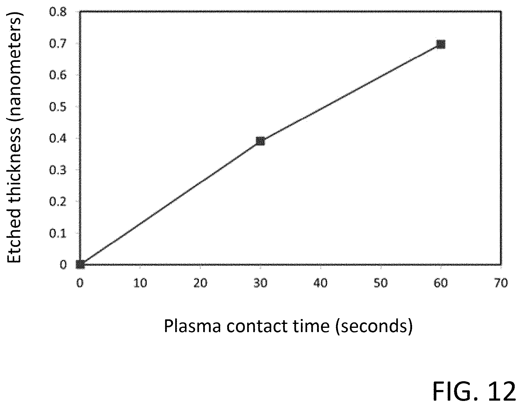
D00013
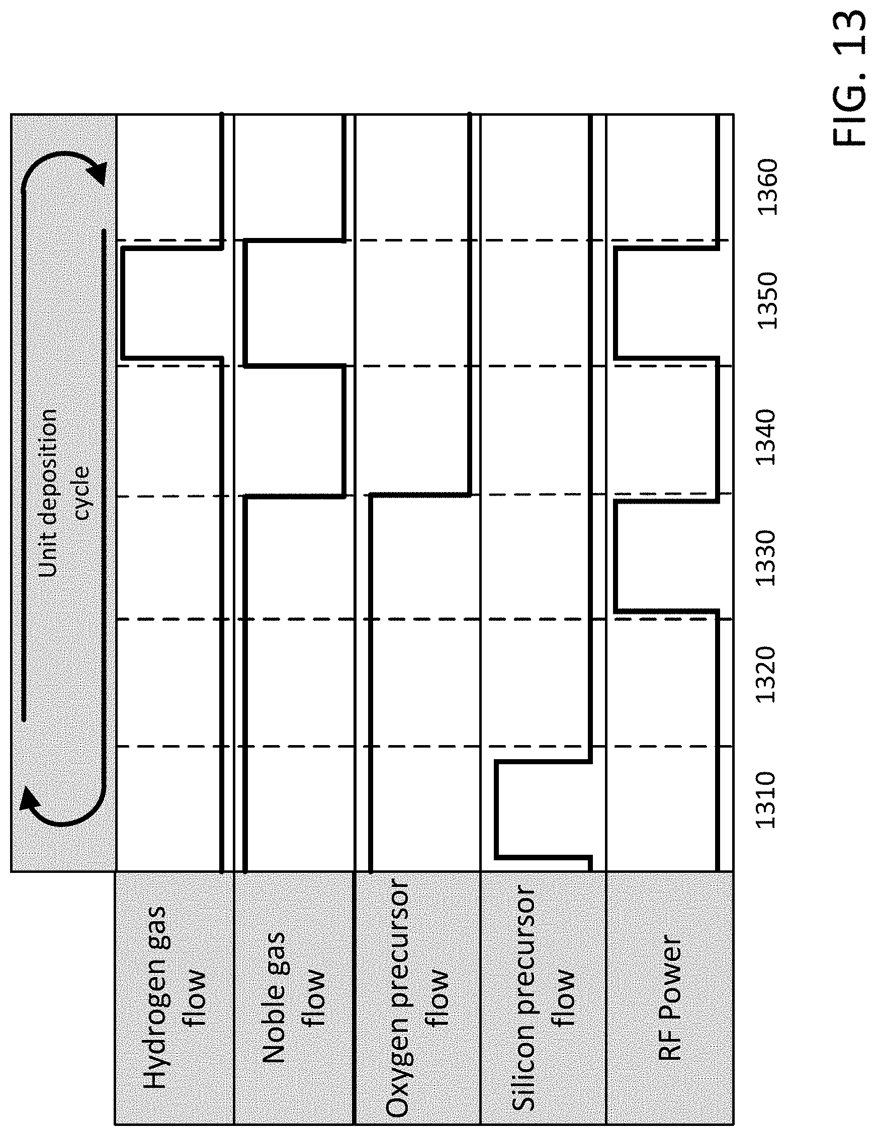
D00014

D00015

XML
uspto.report is an independent third-party trademark research tool that is not affiliated, endorsed, or sponsored by the United States Patent and Trademark Office (USPTO) or any other governmental organization. The information provided by uspto.report is based on publicly available data at the time of writing and is intended for informational purposes only.
While we strive to provide accurate and up-to-date information, we do not guarantee the accuracy, completeness, reliability, or suitability of the information displayed on this site. The use of this site is at your own risk. Any reliance you place on such information is therefore strictly at your own risk.
All official trademark data, including owner information, should be verified by visiting the official USPTO website at www.uspto.gov. This site is not intended to replace professional legal advice and should not be used as a substitute for consulting with a legal professional who is knowledgeable about trademark law.