Semiconductor Device And Method For Fabricating The Same
HUANG; Tse-Yao
U.S. patent application number 16/561513 was filed with the patent office on 2021-03-11 for semiconductor device and method for fabricating the same. The applicant listed for this patent is NANYA TECHNOLOGY CORPORATION. Invention is credited to Tse-Yao HUANG.
| Application Number | 20210074804 16/561513 |
| Document ID | / |
| Family ID | 1000004359931 |
| Filed Date | 2021-03-11 |


View All Diagrams
| United States Patent Application | 20210074804 |
| Kind Code | A1 |
| HUANG; Tse-Yao | March 11, 2021 |
SEMICONDUCTOR DEVICE AND METHOD FOR FABRICATING THE SAME
Abstract
The present application discloses a semiconductor device and a method for fabricating the semiconductor device. The semiconductor device includes a substrate, a conductive feature comprising tungsten positioned above the substrate, a coverage layer comprising tungsten nitride positioned on a top surface of the conductive feature, and a plurality of capacitor structures positioned above the substrate.
| Inventors: | HUANG; Tse-Yao; (TAIPEI CITY, TW) | ||||||||||
| Applicant: |
|
||||||||||
|---|---|---|---|---|---|---|---|---|---|---|---|
| Family ID: | 1000004359931 | ||||||||||
| Appl. No.: | 16/561513 | ||||||||||
| Filed: | September 5, 2019 |
| Current U.S. Class: | 1/1 |
| Current CPC Class: | H01L 21/02271 20130101; H01L 21/02126 20130101; C23C 16/401 20130101; H01L 23/528 20130101; H01L 21/02337 20130101; H01L 21/02332 20130101; H01L 28/40 20130101; H01L 21/02304 20130101 |
| International Class: | H01L 49/02 20060101 H01L049/02; H01L 23/528 20060101 H01L023/528; H01L 21/02 20060101 H01L021/02; C23C 16/40 20060101 C23C016/40 |
Claims
1. A semiconductor device, comprising: a substrate; a conductive feature comprising tungsten positioned above the substrate; a coverage layer comprising tungsten nitride positioned on a top surface of the conductive feature; a plurality of capacitor structures positioned above the substrate; and a plurality of word lines positioned in the substrate and a doped region positioned between an adjacent pair of the plurality of word lines, wherein the conductive feature is positioned on the doped region.
2. The semiconductor device of claim 1, wherein the conductive feature is positioned below the plurality of capacitor structures.
3. The semiconductor device of claim 1, wherein the conductive feature is positioned above the plurality of capacitor structures.
4. (canceled)
5. The semiconductor device of claim 1, further comprising a plurality of isolation structures positioned in the substrate, wherein the plurality of isolation structures are separated from each other and define a plurality of active regions of the substrate.
6. The semiconductor device of claim 5, further comprising a doped region, wherein each of the plurality of active regions intersects two word lines, the doped region is positioned between one of the two word lines and one of the plurality of isolation structures, and the conductive feature is positioned on the doped region.
7. The semiconductor device of claim 6, wherein the two word lines extend along a first direction and the plurality of active regions extend along a direction that is slanted with respect to the first direction.
8. The semiconductor device of claim 1, further comprising a plurality of bit line contacts positioned above the substrate and a plurality of bit lines positioned above the substrate, wherein one of the plurality of bit line contacts is positioned on the coverage layer and is positioned under one of the plurality of bit lines.
9. The semiconductor device of claim 8, wherein the plurality of bit lines are formed as wavy lines.
10. The semiconductor device of claim 4, further comprising a plurality of bit lines positioned above the substrate, wherein the plurality of word lines extend along a first direction, the plurality of bit lines extend along a second direction, and the first direction is perpendicular to the second direction.
11. The semiconductor device of claim 1, wherein the plurality of capacitor structures comprise a plurality of bottom electrodes inwardly positioned above the substrate, a capacitor insulating layer positioned on the plurality of bottom electrodes, and a top electrode positioned on the capacitor insulating layer.
12. A method for fabricating a semiconductor device, comprising: providing a substrate; forming a conductive feature comprising tungsten positioned above the substrate; forming a coverage layer comprising tungsten nitride positioned on a top surface of the conductive feature; and cleaning the conductive feature before forming a coverage layer comprising tungsten nitride positioned on a top surface of the conductive feature, wherein cleaning the conductive feature comprises applying a reducing agent to the top surface of the conductive feature, and the reducing agent is titanium tetrachloride, tantalum tetrachloride, or a combination thereof.
13. (canceled)
14. The method for fabricating the semiconductor device of claim 12, further comprising forming a plurality of capacitor structures positioned above the substrate.
15. The method for fabricating the semiconductor device of claim 14, wherein the conductive feature is positioned below the plurality of capacitor structures.
16. The method for fabricating the semiconductor device of claim 14, wherein the conductive feature is positioned above the plurality of capacitor structures.
17. The method for fabricating the semiconductor device of claim 14, further comprising forming a plurality of word lines positioned in the substrate and a doped region positioned between an adjacent pair of the plurality of word lines, wherein the conductive feature is positioned on the doped region.
18. The method for fabricating the semiconductor device of claim 14, further comprising forming a plurality of bit line contacts and a plurality of bit lines, wherein one of the plurality of bit line contacts is positioned on the coverage layer and is positioned under one of the plurality of bit lines.
19. The method for fabricating the semiconductor device of claim 18, wherein the plurality of bit lines are formed as wavy lines.
20. The method for fabricating the semiconductor device of claim 18, wherein the plurality of capacitor structures comprise a plurality of bottom electrodes inwardly positioned above the substrate, a capacitor insulating layer positioned on the plurality of bottom electrodes, and a top electrode positioned on the capacitor insulating layer.
Description
TECHNICAL FIELD
[0001] The present disclosure relates to a semiconductor device and a method for fabricating the semiconductor device, and more particularly, to a semiconductor device with coverage layer and a method for fabricating the semiconductor device with coverage layer.
DISCUSSION OF THE BACKGROUND
[0002] Semiconductor devices are used in a variety of electronic applications, such as personal computers, cell phones, digital cameras, and other electronic equipment. The dimensions of semiconductor devices are continuously being scaled down to meet the increasing demand of computing ability. However, a variety of issues arise during the scaling-down process and impact the final electrical characteristics, quality, and yield. Therefore, challenges remain in achieving improved performance, quality, yield, and reliability.
[0003] This Discussion of the Background section is provided for background information only. The statements in this Discussion of the Background are not an admission that the subject matter disclosed in this section constitutes prior art to the present disclosure, and no part of this Discussion of the Background section may be used as an admission that any part of this application, including this Discussion of the Background section, constitutes prior art to the present disclosure.
SUMMARY
[0004] One aspect of the present disclosure provides a semiconductor device including a substrate, a conductive feature comprising tungsten positioned above the substrate, a coverage layer comprising tungsten nitride positioned on a top surface of the conductive feature, and a plurality of capacitor structures positioned above the substrate.
[0005] In some embodiments, the conductive feature is positioned below the plurality of capacitor structures.
[0006] In some embodiments, the conductive feature is positioned above the plurality of capacitor structures.
[0007] In some embodiments, the semiconductor device further comprises a plurality of word lines positioned in the substrate and a doped region positioned between an adjacent pair of the plurality of word lines, wherein the conductive feature is positioned on the doped region.
[0008] In some embodiments, the semiconductor device further comprises a plurality of isolation structures positioned in the substrate, wherein the plurality of isolation structures are separated from each other and define a plurality of active regions of the substrate.
[0009] In some embodiments, the semiconductor device further comprises a doped region, wherein each of the plurality of active regions intersects two word lines, the doped region is positioned between one of the two word lines and one of the plurality of isolation structures, and the conductive feature is positioned on the doped region.
[0010] In some embodiments, the two word lines extend along a first direction and the plurality of active regions extend along a direction that is slanted with respect to the first direction.
[0011] In some embodiments, the semiconductor device further comprises a plurality of bit line contacts positioned above the substrate and a plurality of bit lines positioned above the substrate, wherein one of the plurality of bit line contacts is positioned on the coverage layer and is positioned under one of the plurality of bit lines.
[0012] In some embodiments, the plurality of bit lines are formed as wavy lines.
[0013] In some embodiments, the semiconductor device further comprises a plurality of bit lines positioned above the substrate, wherein the plurality of word lines extend along a first direction, the plurality of bit lines extend along a second direction, and the first direction is perpendicular to the second direction.
[0014] In some embodiments, the plurality of capacitor structures comprise a plurality of bottom electrodes inwardly positioned above the substrate, a capacitor insulating layer positioned on the plurality of bottom electrodes, and a top electrode positioned on the capacitor insulating layer.
[0015] Another aspect of the present disclosure provides a method for fabricating a semiconductor device including providing a substrate, forming a conductive feature comprising tungsten positioned above the substrate, and forming a coverage layer comprising tungsten nitride positioned on a top surface of the conductive feature.
[0016] In some embodiments, the method for fabricating the semiconductor device further comprises: cleaning the conductive feature before forming a coverage layer comprising tungsten nitride positioned on a top surface of the conductive feature, wherein cleaning the conductive feature comprises applying a reducing agent to the top surface of the conductive feature, and the reducing agent is titanium tetrachloride, tantalum tetrachloride, or a combination thereof.
[0017] In some embodiments, the method for fabricating the semiconductor device further comprises: forming a plurality of capacitor structures positioned above the substrate.
[0018] In some embodiments, the conductive feature is positioned below the plurality of capacitor structures.
[0019] In some embodiments, the conductive feature is positioned above the plurality of capacitor structures.
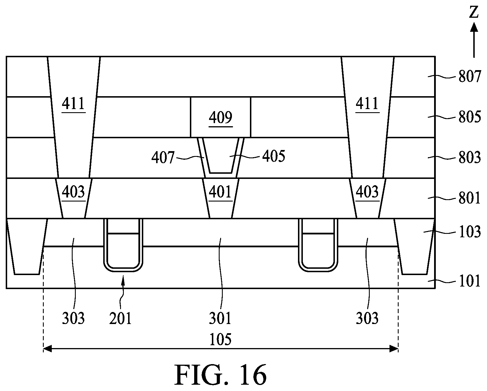
[0020] In some embodiments, the method for fabricating the semiconductor device further comprises: forming a plurality of word lines positioned in the substrate and a doped region positioned between an adjacent pair of the plurality of word lines, wherein the conductive feature is positioned on the doped region.
[0021] In some embodiments, the method for fabricating the semiconductor device further comprises: forming a plurality of bit line contacts and a plurality of bit lines, wherein one of the plurality of bit line contacts is positioned on the coverage layer and is positioned under one of the plurality of bit lines.
[0022] In some embodiments, the plurality of bit lines are formed as wavy lines.
[0023] In some embodiments, the plurality of capacitor structures comprise a plurality of bottom electrodes inwardly positioned above the substrate, a capacitor insulating layer positioned on the plurality of bottom electrodes, and a top electrode positioned on the capacitor insulating layer.
[0024] Due to the design of the semiconductor device of the present disclosure, the coverage layer may reduce formation of defects in the semiconductor device; therefore, the yield of the semiconductor device may be increased.
[0025] The foregoing has outlined rather broadly the features and technical advantages of the present disclosure in order that the detailed description of the disclosure that follows may be better understood. Additional features and advantages of the disclosure will be described hereinafter, and form the subject of the claims of the disclosure. It should be appreciated by those skilled in the art that the conception and specific embodiment disclosed may be readily utilized as a basis for modifying or designing other structures or processes for carrying out the same purposes of the present disclosure. It should also be realized by those skilled in the art that such equivalent constructions do not depart from the spirit and scope of the disclosure as set forth in the appended claims.
BRIEF DESCRIPTION OF THE DRAWINGS
[0026] Aspects of the present disclosure are best understood from the following detailed description when read with the accompanying figures. It should be noted that, in accordance with the standard practice in the industry, various features are not drawn to scale. In fact, the dimensions of the various features may be arbitrarily increased or reduced for clarity of discussion.
[0027] FIG. 1 illustrates, in a flowchart diagram form, a method for fabricating a semiconductor device in accordance with one embodiment of the present disclosure;
[0028] FIGS. 2 and 3 illustrate, in schematic cross-sectional diagrams, part of a flow of fabricating a semiconductor device in accordance with one embodiment of the present disclosure;
[0029] FIG. 4 illustrates, in a schematic top-view diagram, the semiconductor device in accordance with FIG. 3;
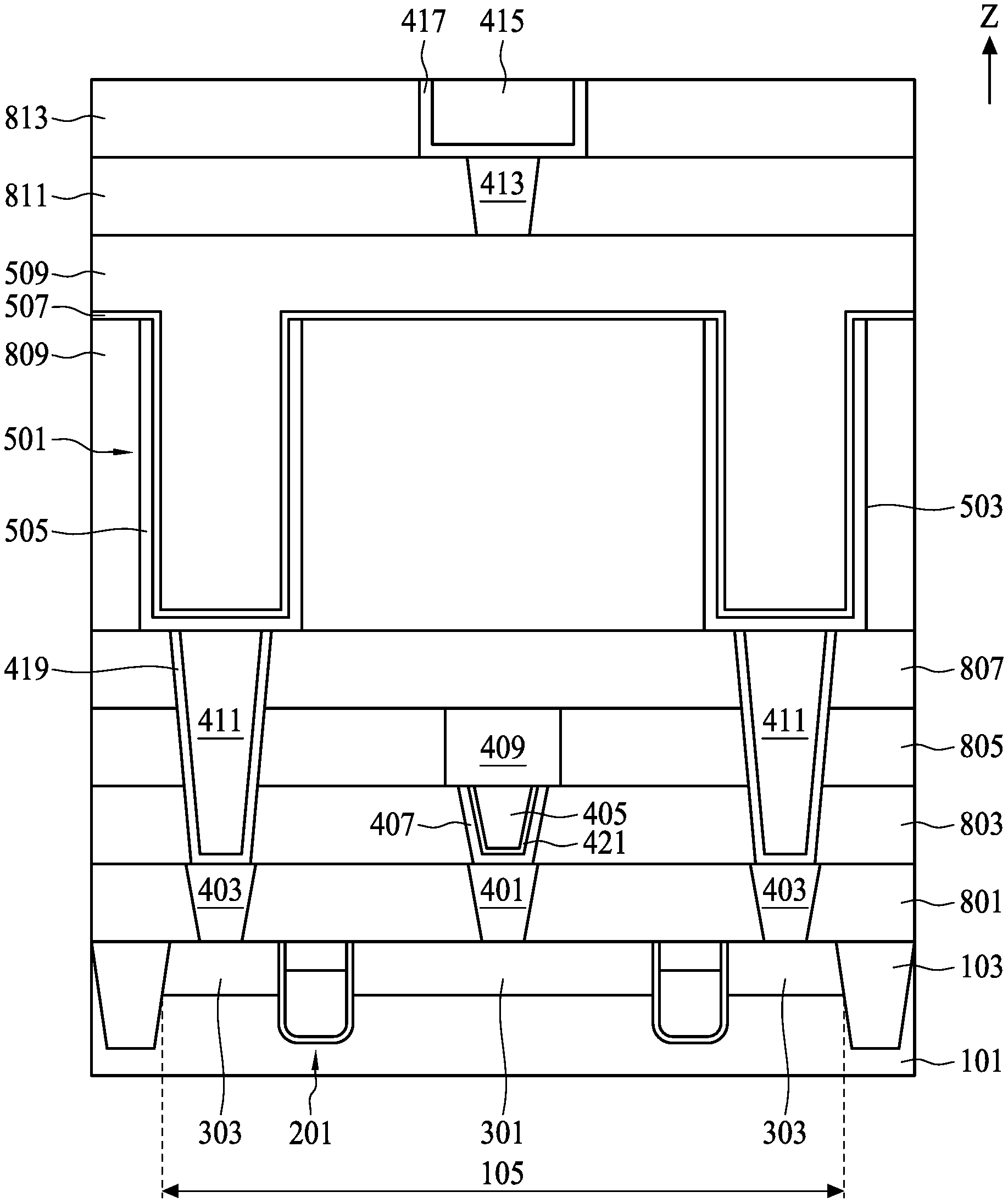
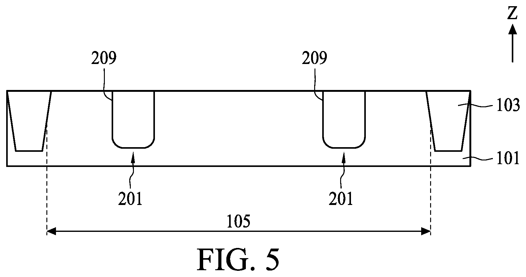
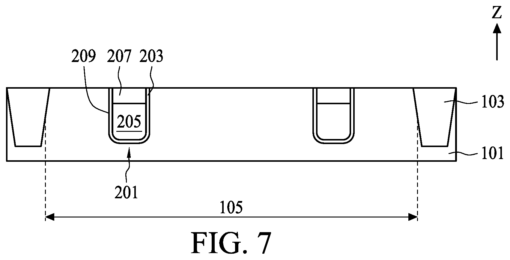
[0030] FIGS. 5 to 7 illustrate, in schematic cross-sectional diagrams, part of the flow of fabricating the semiconductor device in accordance with one embodiment of the present disclosure;
[0031] FIG. 8 illustrates, in a schematic top-view diagram, the semiconductor device in accordance with FIG. 7;
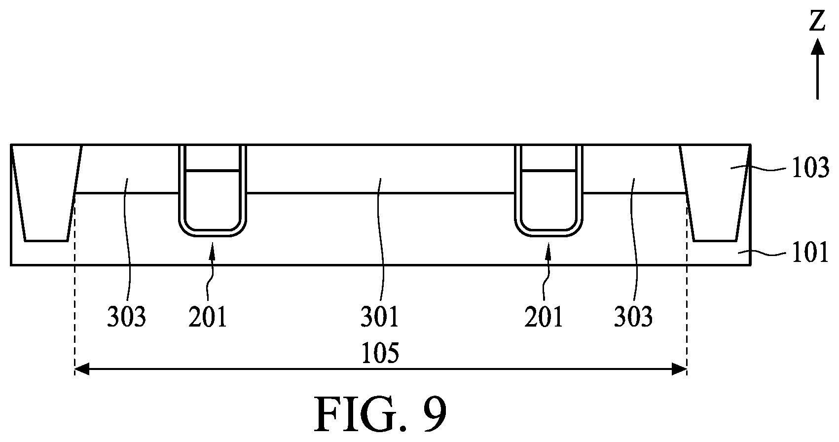
[0032] FIG. 9 illustrates, in a schematic cross-sectional diagram, part of the flow of fabricating the semiconductor device in accordance with one embodiment of the present disclosure;
[0033] FIG. 10 illustrates, in a schematic cross-sectional diagram, part of the flow of fabricating the semiconductor device in accordance with one embodiment of the present disclosure;
[0034] FIG. 11 illustrates, in a schematic top-view diagram, the semiconductor device in accordance with FIG. 10;
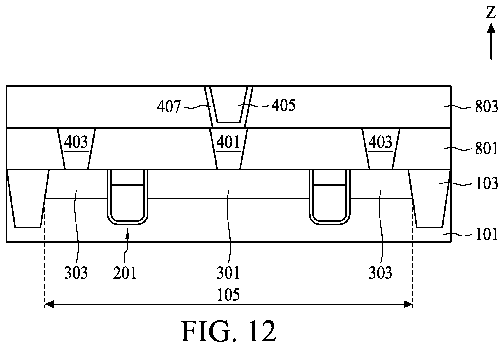
[0035] FIG. 12 illustrates, in a schematic cross-sectional diagram, part of the flow of fabricating the semiconductor device in accordance with one embodiment of the present disclosure;
[0036] FIG. 13 illustrates, in a schematic top-view diagram, the semiconductor device in accordance with FIG. 12;
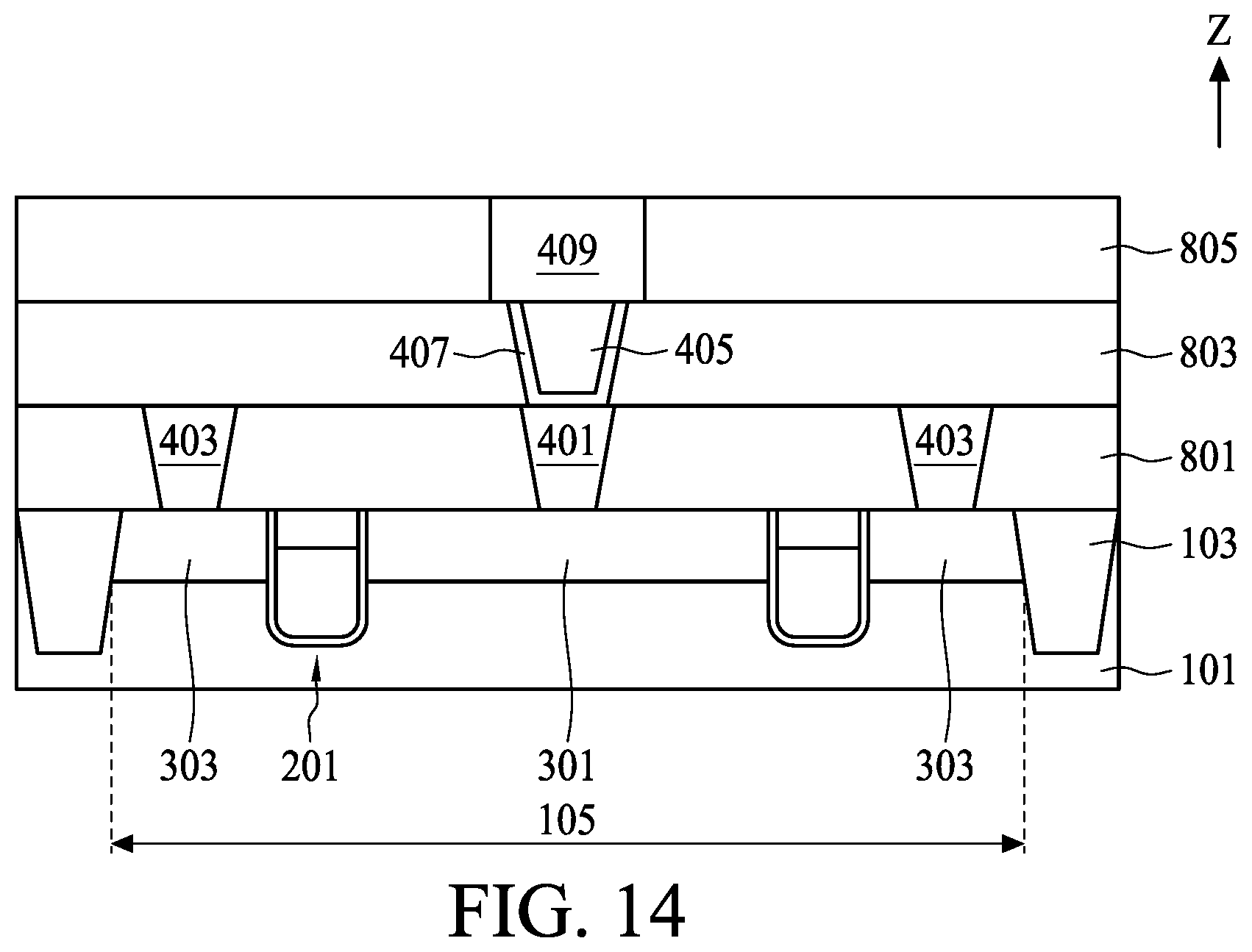
[0037] FIG. 14 illustrates, in a schematic cross-sectional diagram, part of the flow of fabricating the semiconductor device in accordance with one embodiment of the present disclosure;
[0038] FIG. 15 illustrates, in a schematic top-view diagram, the semiconductor device in accordance with FIG. 14;
[0039] FIG. 16 illustrates, in a schematic cross-sectional diagram, part of the flow of fabricating the semiconductor device in accordance with one embodiment of the present disclosure;
[0040] FIGS. 17 to 20 illustrate, in schematic cross-sectional diagrams, part of the flow of fabricating the semiconductor device in accordance with one embodiment of the present disclosure;
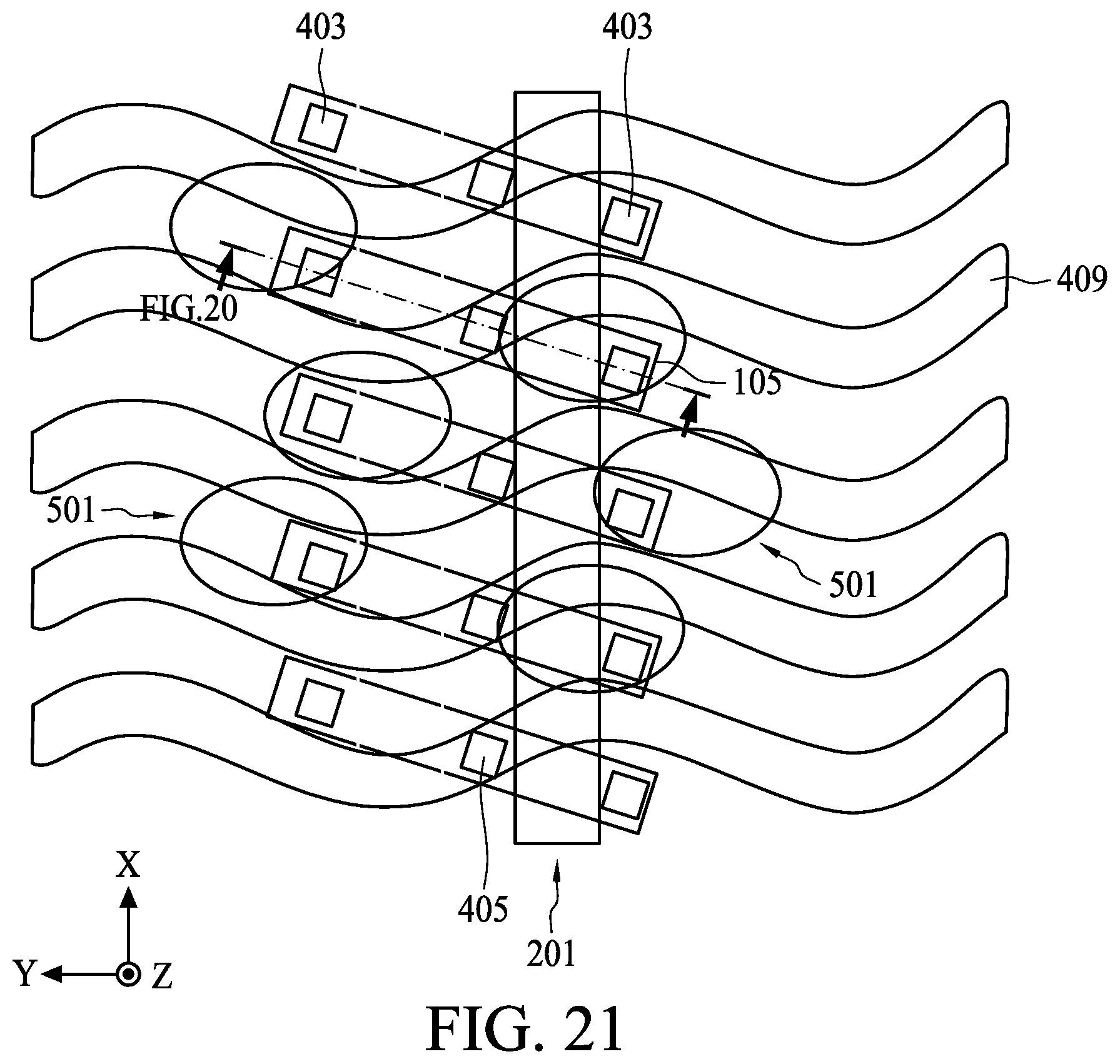
[0041] FIG. 21 illustrates, in a schematic top-view diagram, the semiconductor device in accordance with FIG. 20;
[0042] FIGS. 22 to 24 illustrate, in schematic cross-sectional diagrams, part of the flow of fabricating the semiconductor device in accordance with one embodiment of the present disclosure;
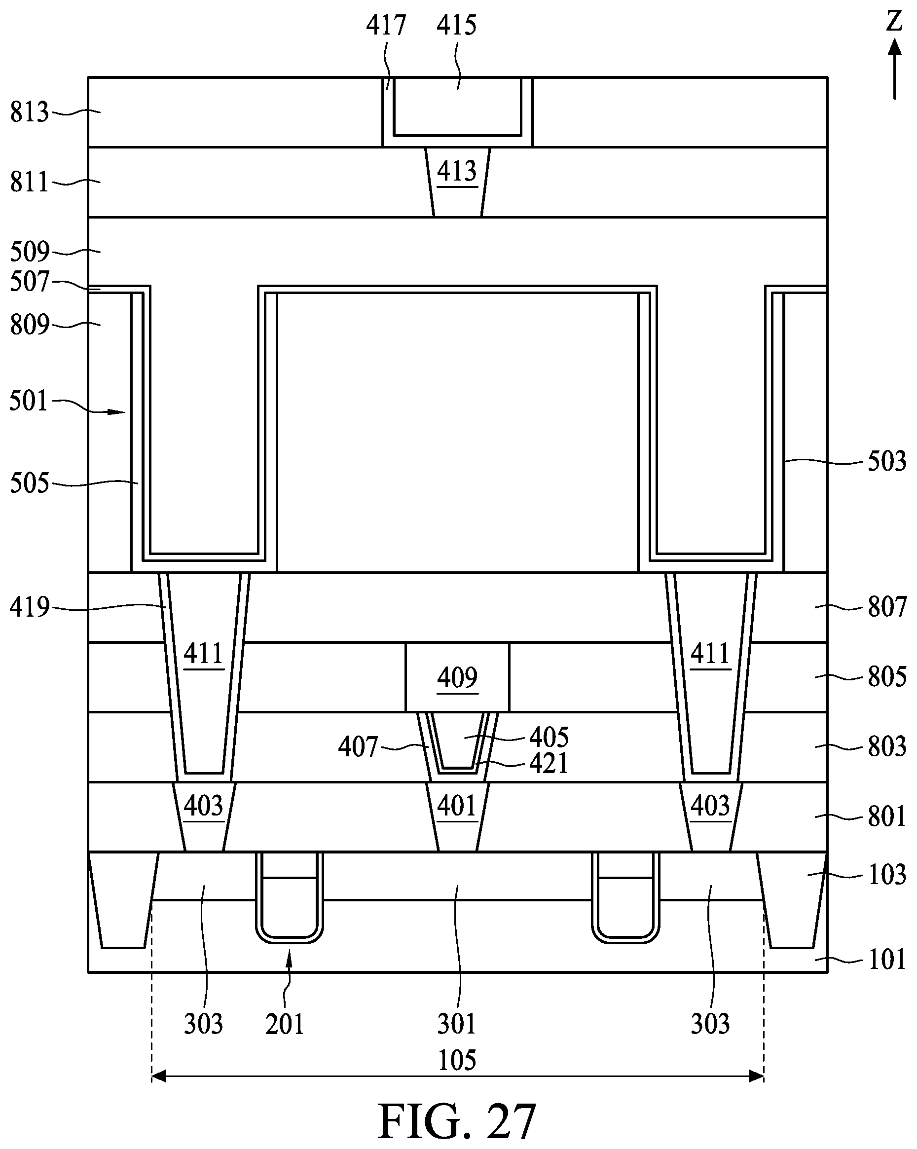
[0043] FIGS. 25 to 27 illustrate, in schematic cross-sectional view diagrams, some semiconductor devices in accordance with some embodiments of the present disclosure.
DETAILED DESCRIPTION
[0044] The following disclosure provides many different embodiments, or examples, for implementing different features of the provided subject matter. Specific examples of components and arrangements are described below to simplify the present disclosure. These are, of course, merely examples and are not intended to be limiting. For example, the formation of a first feature over or on a second feature in the description that follows may include embodiments in which the first and second features are formed in direct contact, and may also include embodiments in which additional features may be formed between the first and second features, such that the first and second features may not be in direct contact. In addition, the present disclosure may repeat reference numerals and/or letters in the various examples. This repetition is for the purpose of simplicity and clarity and does not in itself dictate a relationship between the various embodiments and/or configurations discussed.
[0045] Further, spatially relative terms, such as "beneath," "below," "lower," "above," "upper" and the like, may be used herein for ease of description to describe one element or feature's relationship to another element(s) or feature(s) as illustrated in the figures. The spatially relative terms are intended to encompass different orientations of the device in use or operation in addition to the orientation depicted in the figures. The apparatus may be otherwise oriented (rotated 90 degrees or at other orientations) and the spatially relative descriptors used herein may likewise be interpreted accordingly.
[0046] It will be understood that when an element or layer is referred to as being "connected to," or "coupled to" another element or layer, it can be directly connected to or coupled to another element or layer or intervening elements or layers may be present.
[0047] It will be understood that, although the terms first, second, etc. may be used herein to describe various elements, these elements should not be limited by these terms. Unless indicated otherwise, these terms are only used to distinguish one element from another element. Thus, for example, a first element, a first component or a first section discussed below could be termed a second element, a second component or a second section without departing from the teachings of the present disclosure.
[0048] Unless the context indicates otherwise, terms such as "same," "equal," "planar," or "coplanar," as used herein when referring to orientation, layout, location, shapes, sizes, amounts, or other measures do not necessarily mean an exactly identical orientation, layout, location, shape, size, amount, or other measure, but are intended to encompass nearly identical orientation, layout, location, shapes, sizes, amounts, or other measures within acceptable variations that may occur, for example, due to manufacturing processes. The term "substantially" may be used herein to reflect this meaning. For example, items described as "substantially the same," "substantially equal," or "substantially planar," may be exactly the same, equal, or planar, or may be the same, equal, or planar within acceptable variations that may occur, for example, due to manufacturing processes.
[0049] In the present disclosure, a semiconductor device generally means a device which can function by utilizing semiconductor characteristics, and an electro-optic device, a light-emitting display device, a semiconductor circuit, and an electronic device are all included in the category of the semiconductor device.
[0050] Note that, in the description of the present disclosure, above (or up) corresponds to the direction of the arrow of the direction Z, and below (or down) corresponds to the opposite direction of the arrow of the direction Z.
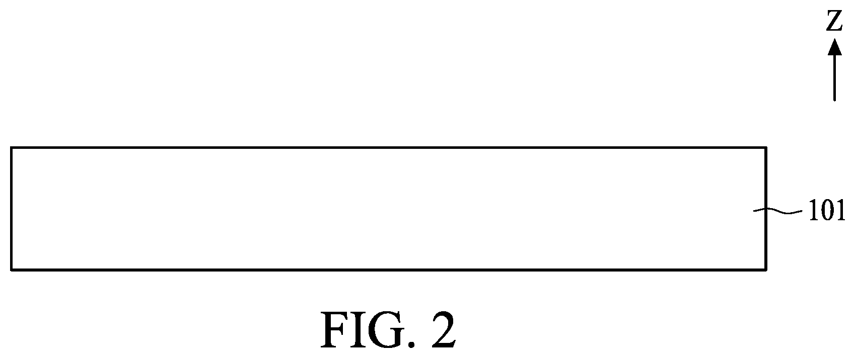
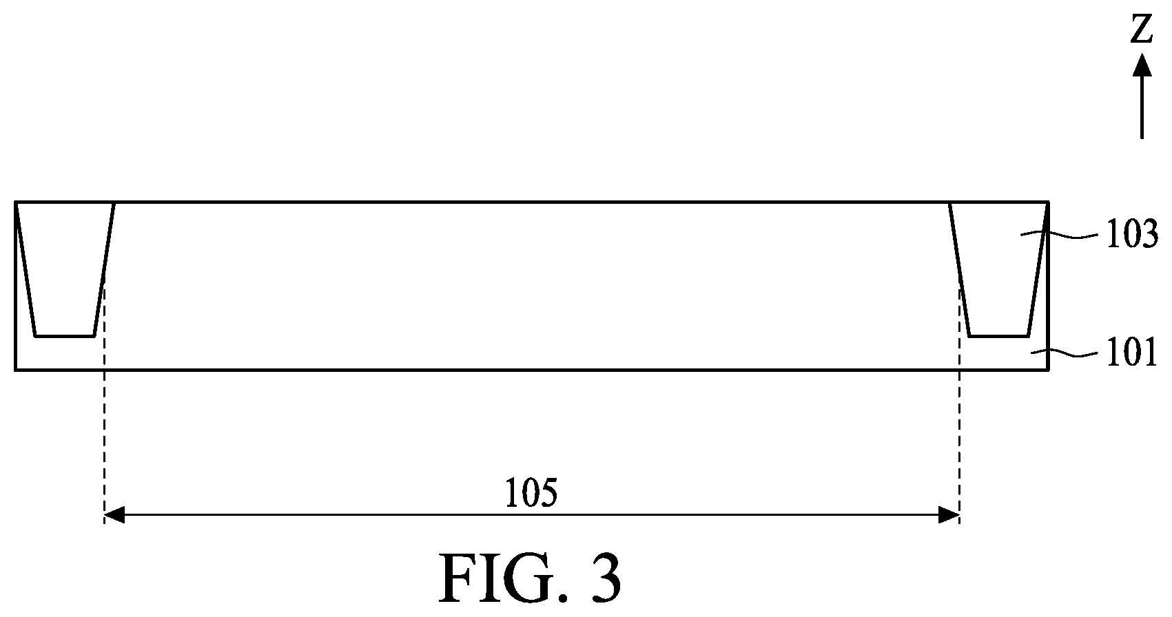
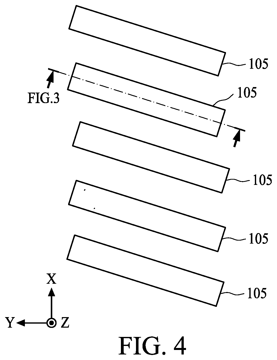
[0051] FIG. 1 illustrates, in a flowchart diagram form, a method 10 for fabricating a semiconductor device in accordance with one embodiment of the present disclosure. FIGS. 2 and 3 illustrate, in schematic cross-sectional diagrams, part of a flow of fabricating a semiconductor device in accordance with one embodiment of the present disclosure. FIG. 4 illustrates, in a schematic top-view diagram, the semiconductor device in accordance with FIG. 3.
[0052] With reference to FIGS. 1 and 2, at step S11, a substrate 101 may be provided. The substrate 101 may be formed of, for example, silicon, doped silicon, silicon germanium, silicon on insulator, silicon on sapphire, silicon germanium on insulator, silicon carbide, germanium, gallium arsenide, gallium phosphide, gallium arsenide phosphide, indium phosphide, or indium gallium phosphide.
[0053] With reference to FIGS. 3 and 4, at step S13, a plurality of isolation structures 103 may be formed in the substrate 101. The plurality of isolation structures 103 are separated from each other in a cross-sectional view and define a plurality of active regions 105. The plurality of isolation structures 103 may be formed of, for example, an insulating material such as silicon oxide, silicon nitride, silicon oxynitride, silicon nitride oxide, fluoride-doped silicate, or the like. The plurality of active regions 105 may extend in a direction slanted with respect to a direction X in a top-view diagram. Note that, in the present disclosure, silicon oxynitride refers to a substance which contains silicon, nitrogen, and oxygen and in which a proportion of oxygen is greater than that of nitrogen. Silicon nitride oxide refers to a substance which contains silicon, oxygen, and nitrogen and in which a proportion of nitrogen is greater than that of oxygen.
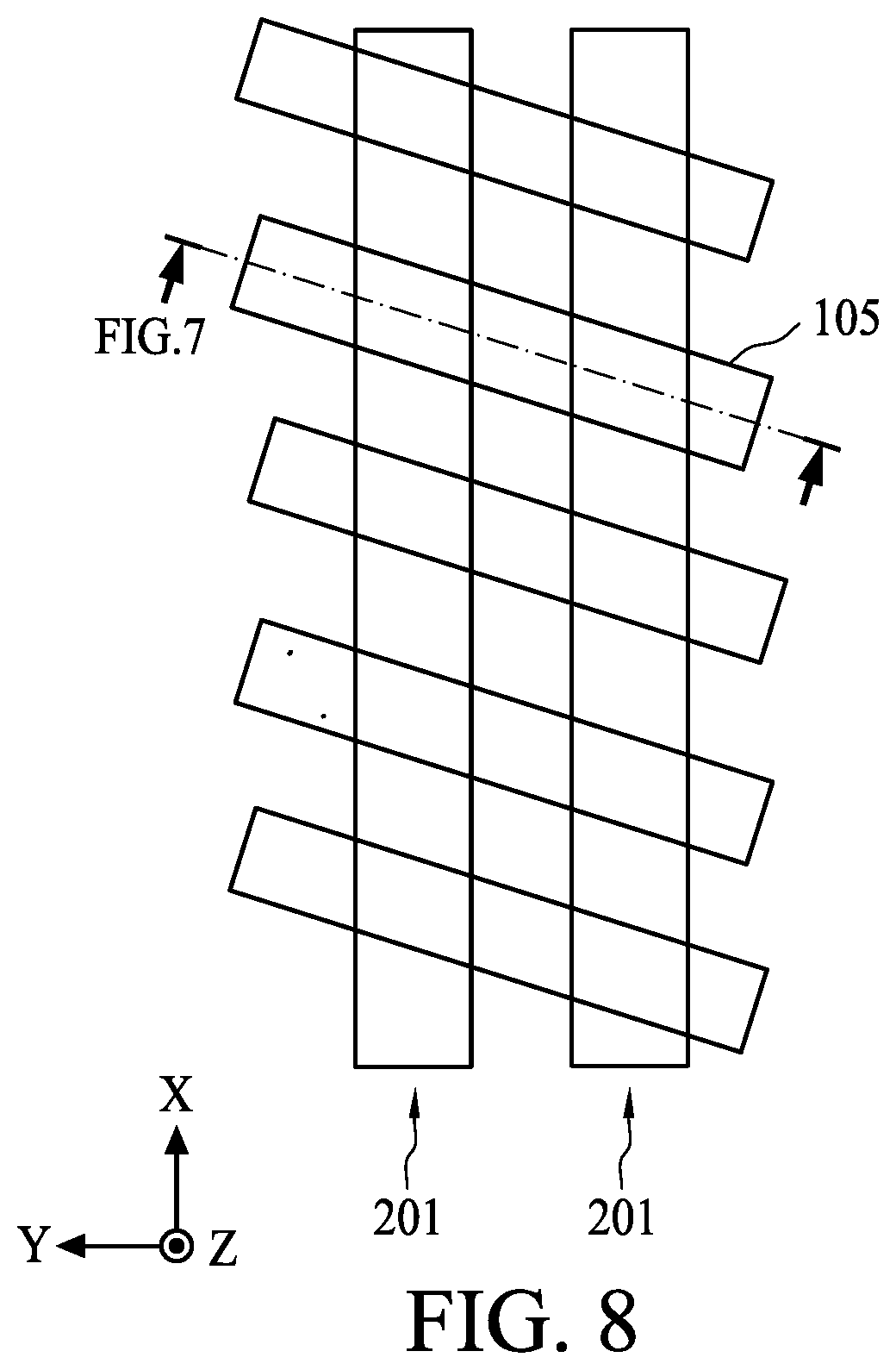
[0054] FIGS. 5 to 7 illustrate, in schematic cross-sectional diagrams, part of the flow of fabricating the semiconductor device in accordance with one embodiment of the present disclosure. FIG. 8 illustrates, in a schematic top-view diagram, the semiconductor device in accordance with FIG. 7.
[0055] With reference to FIG. 1 and FIGS. 5 to 8, at step S15, a plurality of word lines 103 may be formed in the substrate 101. In the embodiment depicted, the plurality of word lines 103 may extend along the direction X. Each one of the plurality of word lines 201 includes a bottom layer 203, a middle layer 205, a top layer 207, and a trench opening 209. With reference to FIG. 5, in the embodiment depicted, a photolithography process may be used to pattern the substrate 101 to define positions of a plurality of trench openings 209. An etch process, such as an anisotropic dry etch process, may be performed to form the plurality of trench openings 209 in the substrate 101. With reference to FIG. 6, after the etch process, the plurality of bottom layers 203 may be correspondingly formed and attached to sidewalls of the plurality of trench openings 209 and bottoms of the plurality of trench openings 209. The plurality of bottom layers 203 may be formed of, for example, silicon oxide, silicon oxynitride, silicon nitride oxide, silicon nitride, or the like.
[0056] With reference to FIGS. 7 and 8, the plurality of middle layers 205 may be correspondingly formed on the plurality of bottom layers 203. Top surfaces of the plurality of middle layers 205 may be lower than a top surface of the substrate 101. The plurality of middle layers 205 may be formed of, for example, doped polysilicon, metal material, or metal silicide. Metal silicide may be, for example, nickel silicide, platinum silicide, titanium silicide, molybdenum silicide, cobalt silicide, tantalum silicide, tungsten silicide, or the like. The plurality of top layers 207 may be correspondingly formed on the plurality of middle layers 205. Top surfaces of the plurality of top layers 207 may be at the same vertical level as the top surface of the substrate 101. The plurality of top layers 207 may be formed of, for example, silicon oxide, silicon oxynitride, silicon nitride oxide, silicon nitride, or the like.
[0057] FIG. 9 illustrates, in a schematic cross-sectional diagram, part of the flow of fabricating the semiconductor device in accordance with one embodiment of the present disclosure.
[0058] With reference to FIG. 1 and FIG. 9, at step S17, a plurality of doped regions may be formed in the plurality of active regions 105 of the substrate 101. The plurality of doped regions may include a first doped region 301 and second doped regions 303. The first doped region 301 is disposed between an adjacent pair of the plurality of word lines 201. The second doped regions 303 are respectively disposed between the plurality of isolation structures 103 and the plurality of word lines 201. The first doped region 301 and the second doped regions 303 are respectively doped with a dopant such as phosphorus, arsenic, or antimony. The first doped region 301 and the second doped regions respectively have dopant concentrations ranging from about 1E17 atoms/cm.sup.3 to about 1E19 atoms/cm.sup.3.
[0059] FIG. 10 illustrates, in a schematic cross-sectional diagram, part of the flow of fabricating the semiconductor device in accordance with one embodiment of the present disclosure. FIG. 11 illustrates, in a schematic top-view diagram, the semiconductor device in accordance with FIG. 10.
[0060] With reference to FIG. 1 and FIGS. 10 and 11, at step S19, a plurality of contacts may be formed above the substrate 101. A first insulating film 801 may be formed on the substrate 101. The first insulating film 801 may be formed of, for example, silicon nitride, silicon oxide, silicon oxynitride, undoped silica glass, borosilica glass, phosphosilica glass, borophosphosilica glass, or a combination thereof, but is not limited thereto. The plurality of contacts may be formed in the first insulating film 801. The plurality of contacts may include a first contact 401 and second contacts 403. A photolithography process may be used to pattern the first insulating film 801 to define positions of the plurality of contacts. An etch process, such as an anisotropic dry etch process, may be performed after the photolithography process to form a plurality of contact openings in the first insulating film 801. After the etch process, a conductive material, for example, aluminum, copper, tungsten, cobalt, or other suitable metal or metal alloy is deposited, by a metallization process such as chemical vapor deposition, physical vapor deposition, sputtering, or the like, in the plurality of contact openings to form the plurality of contacts. A planarization process, such as chemical mechanical polishing, may be performed after the metallization process to remove excess deposited material and provide a substantially flat surface for subsequent processing steps.
[0061] Specifically, with reference to FIGS. 10 and 11, the first contact 401 is disposed on the first doped region 301 and is electrically connected to the first doped region 301. The second contacts 403 are respectively disposed on the second doped regions 303 and are respectively electrically connected to the second doped regions 303. In the embodiment depicted, the first contact 401 is formed including tungsten. In addition, the second contacts 403 are formed including tungsten. Defects may be easily formed on a top surface of the first contact 401 formed including tungsten when the top surface of the first contact 401 is exposed to oxygen or air. The defects may affect the yield of the semiconductor device.
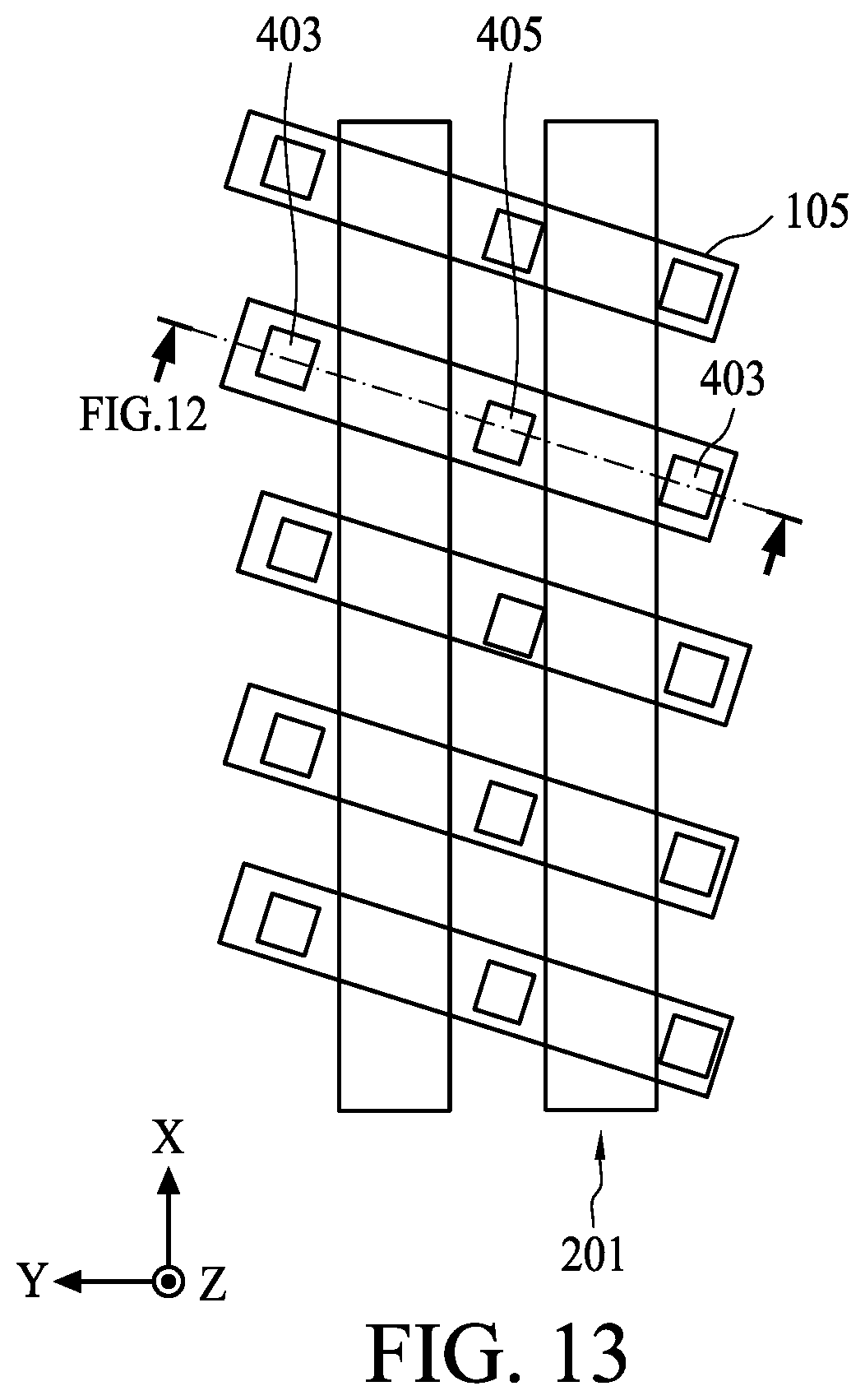
[0062] FIG. 12 illustrates, in a schematic cross-sectional diagram, part of the flow of fabricating the semiconductor device in accordance with one embodiment of the present disclosure. FIG. 13 illustrates, in a schematic top-view diagram, the semiconductor device in accordance with FIG. 12.
[0063] With reference to FIG. 1 and FIGS. 12 and 13, at step S21, a plurality of bit line contacts 405 may be formed above the substrate 101. (Only one bit line contact 405 is shown in FIG. 12.) A second insulating film 803 may be formed on the first insulating film 801. The second insulating film 803 may be formed of a same material as the material of the first insulating film 801, but is not limited thereto. A photolithography process may be used to pattern the second insulating film 803 to define positions of the plurality of bit line contacts 405. An etch process, such as an anisotropic dry etch process, may be performed after the photolithography process to form a plurality of bit line contact openings in the second insulating film 803. A top surface of the first contact 401 may be exposed through the plurality of bit line contact openings. A cleaning process using a reducing agent may be optionally performed to remove the defects on the top surface of the first contact 401 formed including tungsten. The reducing agent may be titanium tetrachloride, tantalum tetrachloride, or a combination thereof.
[0064] With reference to FIGS. 12 and 13, after the cleaning process, a first coverage layer 407 including tungsten nitride may be formed to cover bottoms and sidewalls of the plurality of bit line contact openings. The first coverage layer 407 may prevent the top surface of the first contact 401 formed including tungsten from being exposed to oxygen or air; therefore, the first coverage layer 407 may reduce formation of the defects on the top surface of the first contact 401 formed including tungsten. A conductive material, for example, aluminum, copper, tungsten, cobalt, or other suitable metal or metal alloy is deposited, by a metallization process such as chemical vapor deposition, physical vapor deposition, sputtering, or the like, in the plurality of bit line contact openings to form the plurality of bit line contacts 405. A planarization process, such as chemical mechanical polishing, may be performed after the metallization process to remove excess deposited material and provide a substantially flat surface for subsequent processing steps.
[0065] With reference to FIGS. 12 and 13, the plurality of bit line contacts 405 are correspondingly electrically connected to the first contacts 401; that is to say, the plurality of bit line contacts 405 are electrically coupled to the first doped region 301.
[0066] FIG. 14 illustrates, in a schematic cross-sectional diagram, part of the flow of fabricating the semiconductor device in accordance with one embodiment of the present disclosure. FIG. 15 illustrates, in a schematic top-view diagram, the semiconductor device in accordance with FIG. 14.
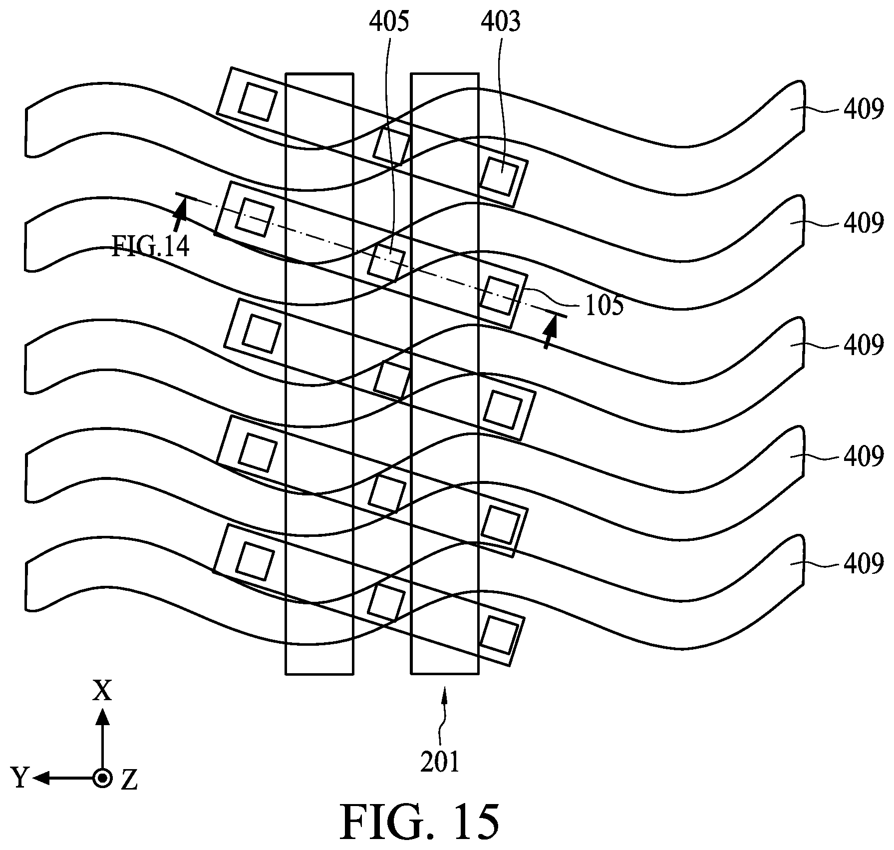
[0067] With reference to FIG. 1 and FIGS. 14 and 15, at step S23, a plurality of bit lines 409 may be formed above the substrate 101. (Only one bit line 409 is shown in FIG. 14.) A third insulating film 805 may be formed on the second insulating film 803. The third insulating film 805 may be formed of a same material as the material of the first insulating film 801, but is not limited thereto. A photolithography process may be used to pattern the third insulating film 805 to define positions of the plurality of bit lines 409. An etch process, such as an anisotropic dry etch process, may be performed after the photolithography process to form a plurality of bit line trench openings in the third insulating film 805. After the etch process, a conductive material, for example, aluminum, copper, tungsten, cobalt, or other suitable metal or metal alloy is deposited, by a metallization process such as chemical vapor deposition, physical vapor deposition, sputtering, or the like, in the plurality of bit line trench openings to form the plurality of bit lines 409. A planarization process, such as chemical mechanical polishing, may be performed after the metallization process to remove excess deposited material and provide a substantially flat surface for subsequent processing steps.
[0068] With reference to FIGS. 14 and 15, the plurality of bit lines 409 may extend along a direction Y and implemented as wavy lines in a top-view diagram. The plurality of bit line contacts 405 are located at intersections of the plurality of bit lines 409 and the plurality of active regions 105. The plurality of bit lines 409 implemented as wavy lines may increase a contact area between the plurality of bit line contacts 405 and the plurality of active regions 105; therefore, a contact resistance between the plurality of bit line contacts 405 and the plurality of active regions 105 may be reduced.
[0069] FIG. 16 illustrates, in a schematic cross-sectional diagram, part of the flow of fabricating the semiconductor device in accordance with one embodiment of the present disclosure.
[0070] With reference to FIG. 1 and FIG. 16, at step S25, a plurality of plugs 411 may be formed above the substrate 101. A fourth insulating film 807 may be formed on the third insulating film 805. The fourth insulating film 807 may be formed of a same material as the material of the first insulating film 801, but is not limited thereto. A photolithography process may be used to pattern the fourth insulating film 807 to define positions of the plurality of plugs 411. An etch process, such as an anisotropic dry etch process, may be performed after the photolithography process to form a plurality of plug openings passing through the fourth insulating film 807, the third insulating film 805, and the second insulating film 803. After the etch process, a conductive material, for example, aluminum, copper, tungsten, cobalt, or other suitable metal or metal alloy is deposited, by a metallization process such as chemical vapor deposition, physical vapor deposition, sputtering, or the like, in the plurality of plug openings to form the plurality of plugs 411. A planarization process, such as chemical mechanical polishing, may be performed after the metallization process to remove excess deposited material and provide a substantially flat surface for subsequent processing steps.
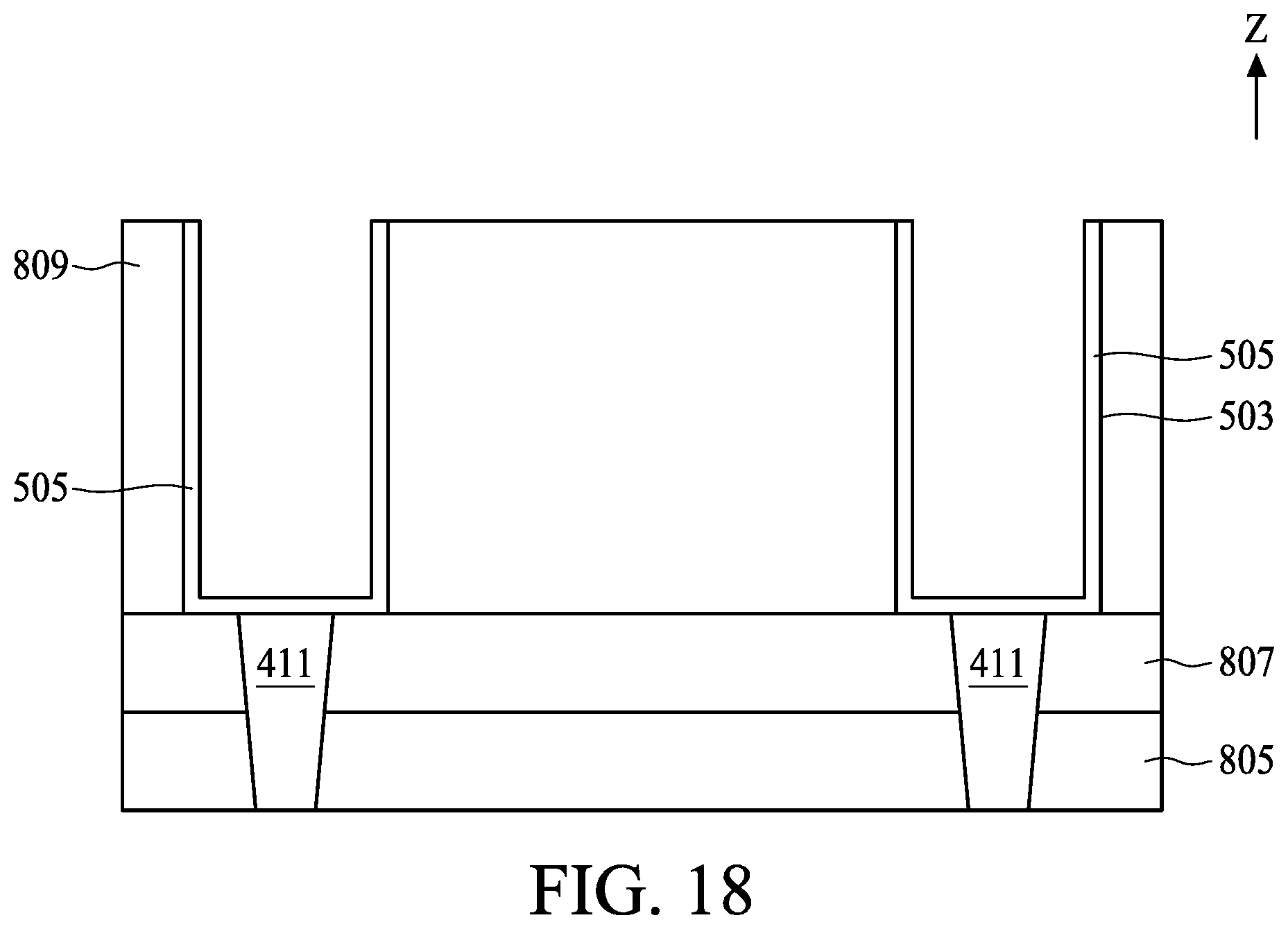
[0071] FIGS. 17 to 20 illustrate, in schematic cross-sectional diagrams, part of the flow of fabricating the semiconductor device in accordance with one embodiment of the present disclosure. FIG. 21 illustrates, in a schematic top-view diagram, the semiconductor device in accordance with FIG. 20.
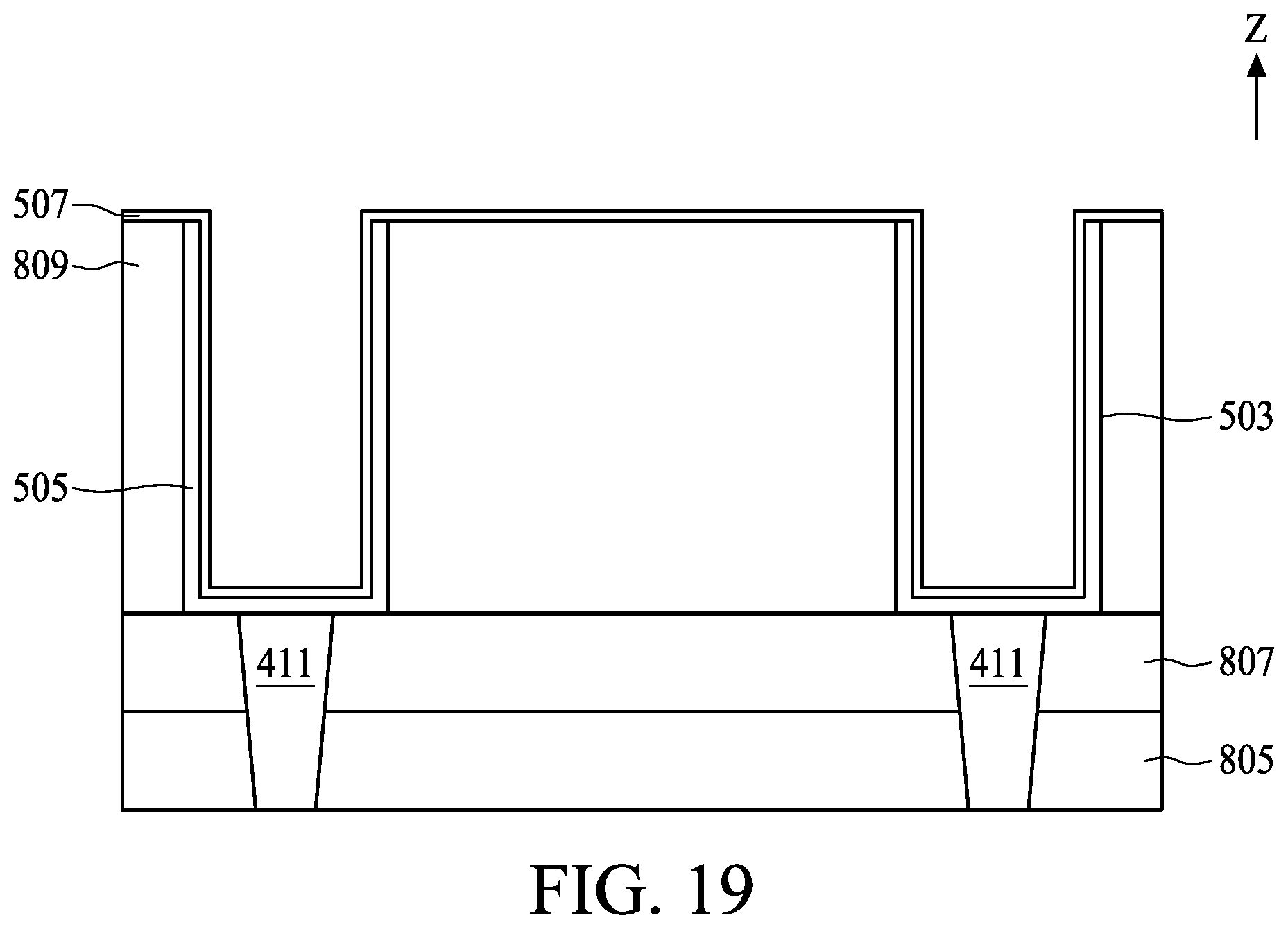
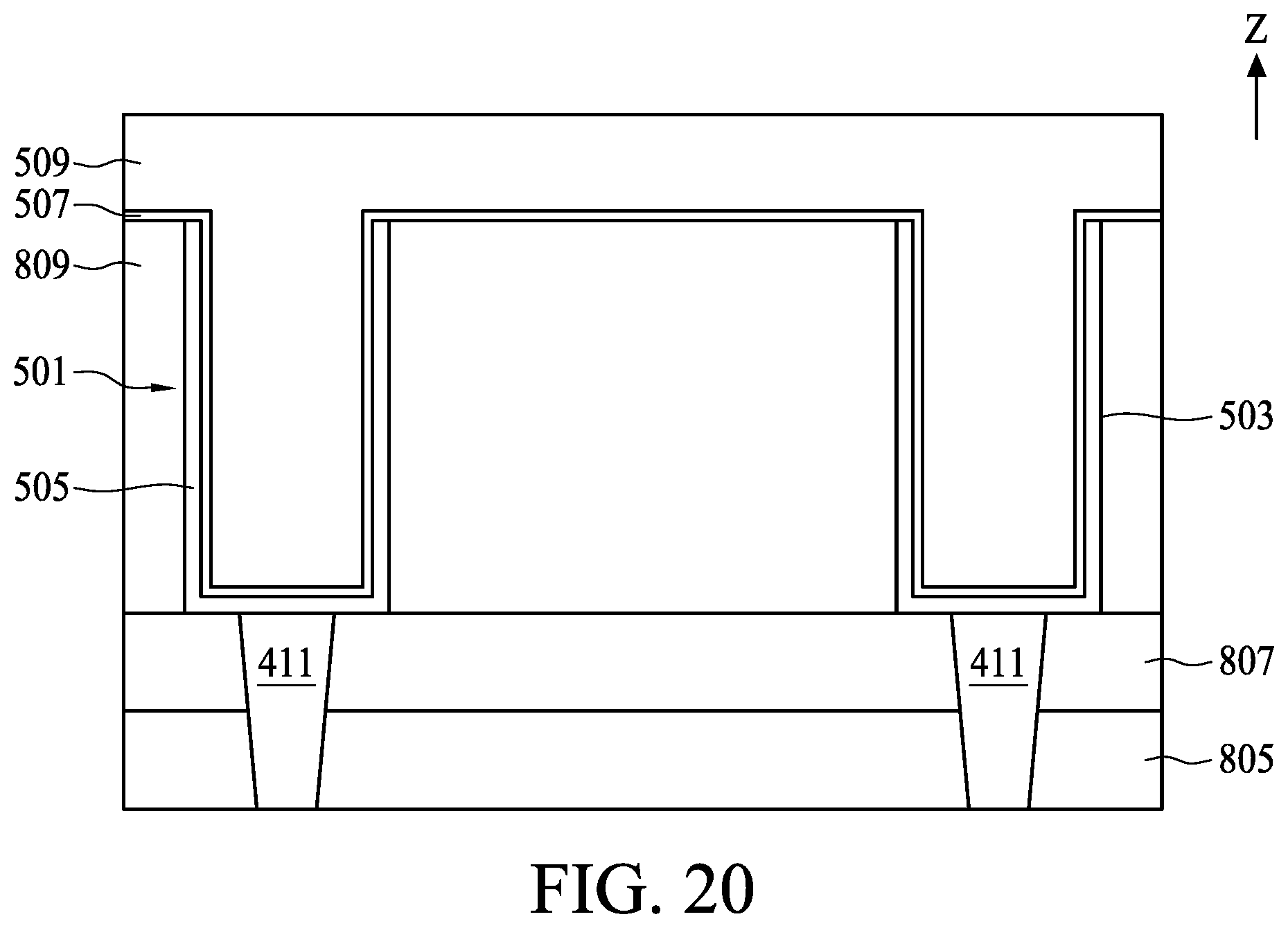
[0072] With reference to FIG. 1 and FIGS. 17 to 21, at step S27, a plurality of capacitor structures 501 may be formed above the substrate 101. Each of the plurality of capacitor structures 501 may include a bottom electrode 505, a capacitor insulating layer 507, and a top electrode 509. With reference to FIG. 17, a fifth insulating film 809 may be formed on the fourth insulating film 807. The fifth insulating film 809 may be formed of a same material as the material of the first insulating film 801, but is not limited thereto. A photolithography process may be used to pattern the fifth insulating film 809 to define positions of a plurality of capacitor trenches 503. An etch process, such as an anisotropic dry etch process, may be performed after the photolithography process to form the plurality of capacitor trenches 503 passing through the fifth insulating film 809. The plurality of plugs 411 may be exposed through the plurality of capacitor trenches 503.
[0073] With reference to FIG. 18, a plurality of bottom electrodes 505 may be correspondingly respectively formed in the plurality of capacitor trenches 503, in other words, the plurality of bottom electrodes 505 may be inwardly formed in the fifth insulating film 809. The plurality of bottom electrodes 601 may be formed of, for example, doped polysilicon, metal silicide, aluminum, copper, or tungsten. The plurality of bottom electrodes 505 may be respectively correspondingly connected to the plurality of plugs 411. With reference to FIG. 19, the capacitor insulating layer 507 may be formed to attach to sidewalls and bottoms of the plurality of bottom electrodes 505 and the top surfaces of the fifth insulating film 809. The capacitor insulating layer 507 may be a single layer or multiple layers. In the embodiment depicted, the capacitor insulating layer 507 may be a single layer or multiple layers. Specifically, the capacitor insulating layer 507 may be a single layer formed of a high dielectric constant material such as barium strontium titanate, lead zirconium titanate, titanium oxide, aluminum oxide, hafnium oxide, yttrium oxide, zirconium oxide, or the like. Alternatively, in another embodiment, the capacitor insulating layer 507 may be multiple layers consisting of silicon oxide, silicon nitride, and silicon oxide.
[0074] With reference to FIGS. 20 and 21, the top electrode 509 may be formed to fill the plurality of capacitor trenches 503 and cover the capacitor insulating layer 507. The top electrode 509 may be formed of, for example, doped polysilicon, copper, or aluminum.
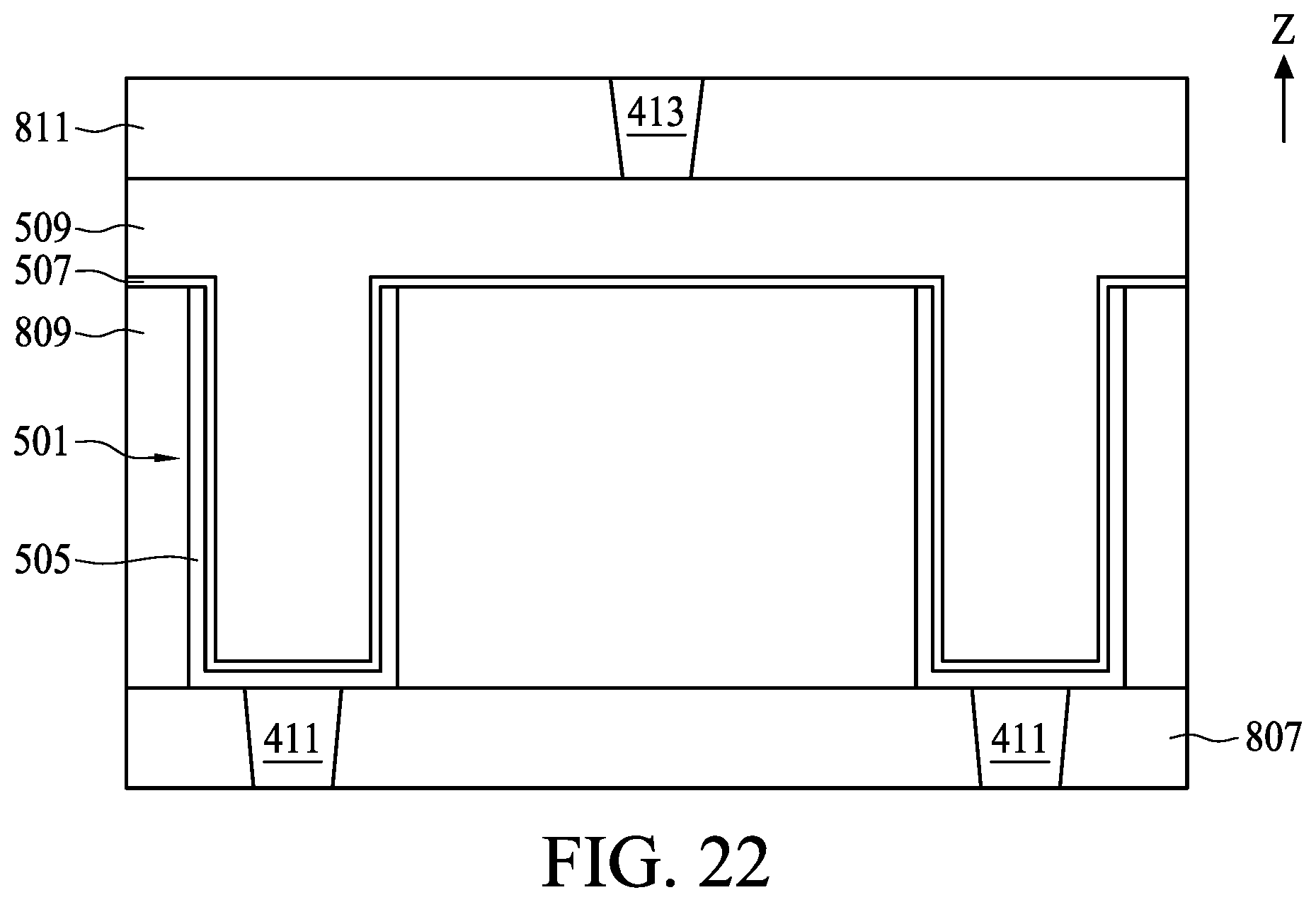
[0075] FIGS. 22 to 24 illustrate, in schematic cross-sectional diagrams, part of the flow of fabricating the semiconductor device in accordance with one embodiment of the present disclosure.
[0076] With reference to FIG. 1 and FIGS. 22 to 24, at step S29, a bottom via 413 and a first conductive layer 415 may be formed above the substrate 101. With reference to FIG. 22, a sixth insulating film 811 may be formed on the fifth insulating film 809. The sixth insulating film 811 may be formed of a same material as the material of the first insulating film 801, but is not limited thereto. A photolithography process may be used to pattern the sixth insulating film 811 to define positions of the bottom via 413. An etch process, such as an anisotropic dry etch process, may be performed after the photolithography process to form a bottom via opening passing through the sixth insulating film 811. After the etch process, a conductive material, for example, aluminum, copper, tungsten, cobalt, or other suitable metal or metal alloy is deposited, by a metallization process such as chemical vapor deposition, physical vapor deposition, sputtering, or the like, in the bottom via opening to form the bottom via 413 in the sixth insulating film 811. A planarization process, such as chemical mechanical polishing, may be performed after the metallization process to remove excess deposited material and provide a substantially flat surface for subsequent processing steps.
[0077] With reference to FIG. 22, in the embodiment depicted, the bottom via 413 is formed including tungsten. Defects may be easily formed on a top surface of the bottom via 413 formed including tungsten when the top surface of the bottom via 413 is exposed to oxygen or air. The defects may affect the yield of the semiconductor device.
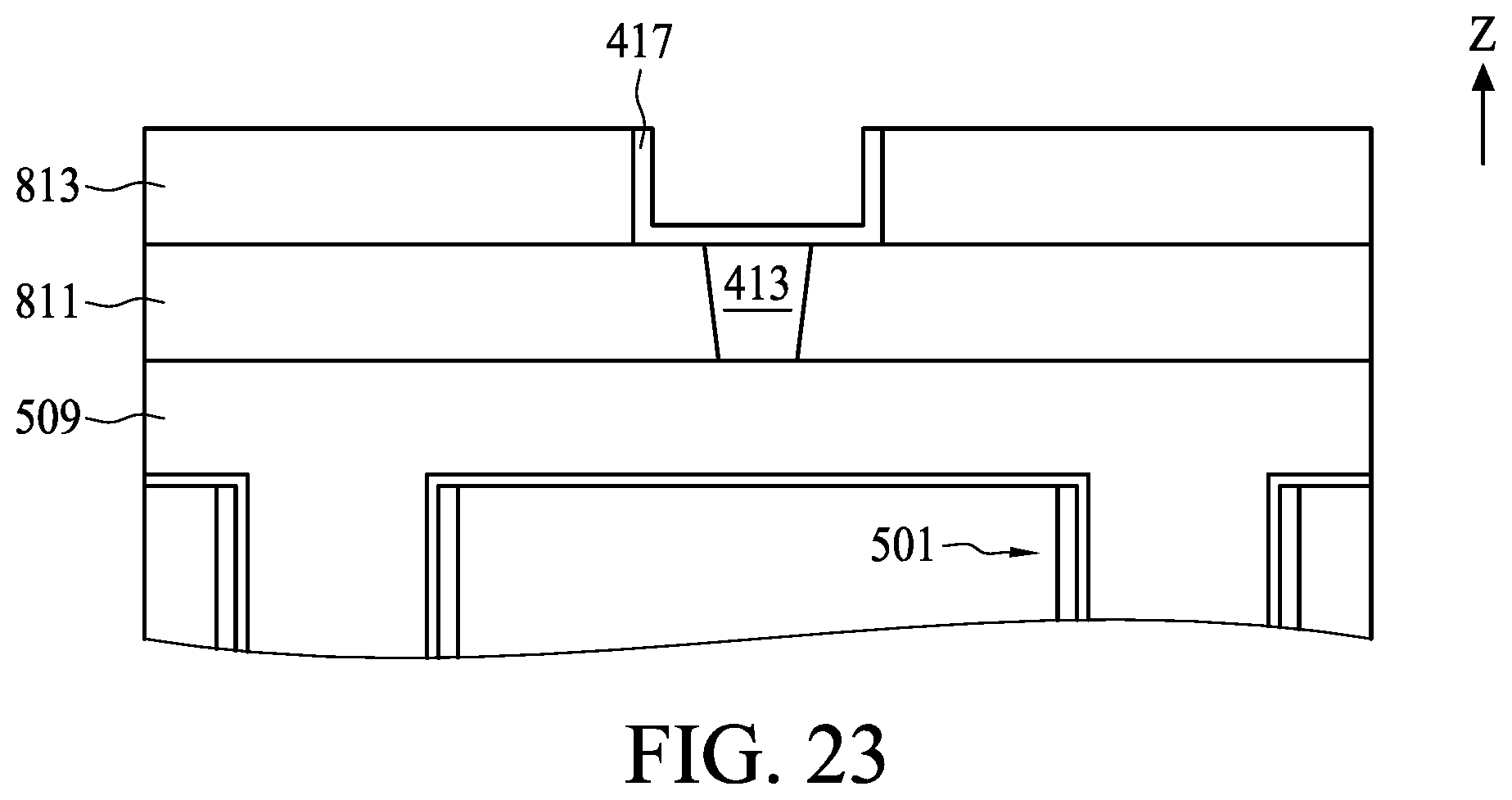
[0078] With reference to FIG. 23, a seventh insulating film 813 may be formed on the sixth insulating film 811. The seventh insulating film 813 may be formed of a same material as the material of the first insulating film 801, but is not limited thereto. A photolithography process may be used to pattern the seventh insulating film 813 to define a position of the first conductive layer 415. An etch process, such as an anisotropic dry etch process, may be performed after the photolithography process to form a first conductive layer trench in the seventh insulating film 813. The top surface of the bottom via 413 may be exposed through the first conductive layer trench. A cleaning process using a reducing agent may be optionally performed to remove the defects on the top surface of the bottom via 413 formed including tungsten. The reducing agent may be titanium tetrachloride, tantalum tetrachloride, or combination thereof.
[0079] With reference to FIGS. 23 and 24, after the cleaning process, a second coverage layer 417 formed including tungsten nitride may be formed to cover a bottom and sidewalls of the first conductive layer trench. The second coverage layer 417 may prevent the top surface of the bottom via 413 formed including tungsten from being exposed to oxygen or air; therefore, the second coverage layer 417 may reduce formation of the defects on the top surface of the bottom via 413 formed including tungsten. A conductive material, for example, aluminum, copper, tungsten, cobalt, or other suitable metal or metal alloy is deposited, by a metallization process such as chemical vapor deposition, physical vapor deposition, sputtering, or the like, in the first conductive layer trench to form the first conductive layer 415. A planarization process, such as chemical mechanical polishing, may be performed after the metallization process to remove excess deposited material and provide a substantially flat surface for subsequent processing steps.
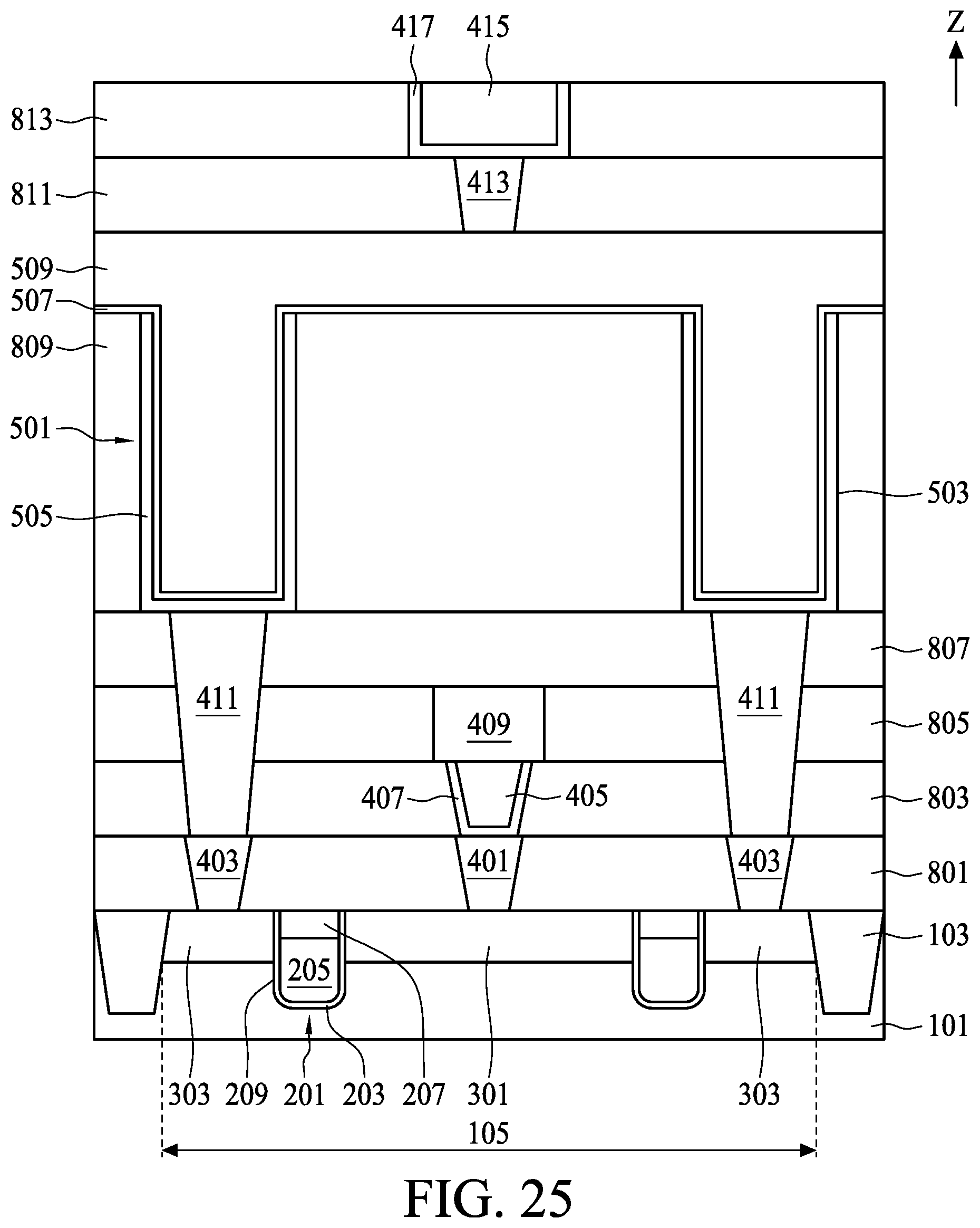
[0080] FIG. 25 illustrates, in a schematic cross-sectional view diagram, a semiconductor device in accordance with one embodiment of the present disclosure.
[0081] With reference to FIG. 25, a semiconductor device may include a substrate 101, a plurality of isolation structures 103, a plurality of word lines 201, a plurality of doped regions, a plurality of insulating films, a plurality of contacts, a plurality of bit line contacts 405, a first coverage layer 407, a plurality of bit lines 409, a plurality of plugs 411, a bottom via 413, a first conductive layer 415, a second coverage layer 417, and a plurality of capacitor structures 501.
[0082] With reference to FIG. 25, the plurality of isolation structures 103 may be disposed in the substrate 101 and separated from each other. The plurality of isolation structures 103 may define a plurality of active regions 105. The plurality of word lines 201 may be disposed in the substrate 101 and separated from each other. Each one of the plurality of word lines 201 includes a bottom layer 203, a middle layer 205, and a top layer 207. The plurality of bottom layers 203 may be respectively inwardly disposed in the substrate 101. The plurality of middle layers 205 may be respectively correspondingly disposed on the plurality of bottom layers 203. Top surfaces of the plurality of middle layers 205 may be lower than a top surface of the substrate 101. The plurality of top layers 207 may be respectively correspondingly disposed on the plurality of middle layers 205. Top surfaces of the plurality of top layers 207 may be at the same vertical level as the top surface of the substrate 101.
[0083] With reference to FIG. 25, a plurality of doped regions may be disposed in the plurality of active regions 105 of the substrate 101. Each of the plurality of doped regions includes a first doped region 301 and second doped regions 303. For each of the plurality of doped regions, the first doped region 301 is disposed between an adjacent pair of the plurality of word lines 201. The second doped regions 303 are respectively disposed between the plurality of isolation structures 103 and the plurality of word lines 201.
[0084] With reference to FIG. 25, the plurality of insulating films may be disposed above the substrate 101. The plurality of insulating films may include a first insulating film 801, a second insulating film 803, a third insulating film 805, a fourth insulating film 807, a fifth insulating film 809, a sixth insulating film 811, and a seventh insulating film 813. The first insulating film 801 may be disposed on the substrate 101. The plurality of contacts may be disposed in the first insulating film 801. The plurality of contacts may include a first contact 401 and second contacts 403. The first contact 401 is disposed on the first doped region 301 and is electrically connected to the first doped region 301. The second contacts 403 are respectively disposed on the second doped regions 303 and are respectively electrically connected to the second doped regions 303. In the embodiment depicted, the first contact 401 is formed including tungsten.
[0085] With reference to FIG. 25, the second insulating film 803 may be disposed on the first insulating film 801. The plurality of bit line contacts 405 may be disposed in the second insulating film 803. (Only bit line contact is shown in FIG. 25.) The first coverage layer 407 may be disposed in the second insulating film 803 and on a top surface of the first contact 401; in other words, the first coverage layer 407 may be disposed between the plurality of bit line contacts 405 and the first contact 401. In addition, the first coverage layer 407 may be disposed on and attached to sidewalls of the plurality of bit line contacts 405. The first coverage layer 407 may include tungsten nitride.
[0086] With reference to FIG. 25, the third insulating film 805 may be disposed on the second insulating film 803. The plurality of bit lines 409 may be disposed in the third insulating film 805 and on the plurality of bit line contacts 405 and the first coverage layer 407. (Only one bit line 409 is shown in FIG. 25.) The fourth insulating film 807 may be disposed on the third insulating film 805. The plurality of plugs 411 may be disposed to pass through the fourth insulating film 807, the third insulating film 805, and the second insulating film 803. The plurality of plugs 411 may be respectively correspondingly electrically connected to the second contacts 403.
[0087] With reference to FIG. 25, the fifth insulating film 809 may be disposed on the fourth insulating film 807. The plurality of capacitor structures 501 may be disposed in the fifth insulating film 809. The plurality of capacitor structures 501 may include a plurality of bottom electrodes 505, a capacitor insulating layer 507, and a top electrode 509. The plurality of bottom electrodes 505 may be inwardly disposed in the fifth insulating film 809 and respectively correspondingly electrically connected to the plurality of plugs 411. The capacitor insulating layer 507 may be disposed on the plurality of bottom electrodes 505. The top electrode 509 may be disposed on the capacitor insulating layer 507.
[0088] With reference to FIG. 25, the sixth insulating film 811 may be disposed on the fifth insulating film 809. The bottom via 413 may be disposed in the sixth insulating film 811 and electrically connected to the top electrode 509. The bottom via 413 may include tungsten. A seventh insulating film 813 may be disposed on the sixth insulating film 811. The first conductive layer 415 may be disposed in the seventh insulating film 813 and above the bottom via 413. The second coverage layer 417 may be disposed on a top surface of the bottom via 413, and the second coverage layer 417 may be disposed between the bottom via 413 and the first conductive layer 415. In addition, the second coverage layer 417 may be disposed on and attached to sidewalls of the first conductive layer 415. The second coverage layer 417 may include tungsten nitride.
[0089] FIGS. 26 and 27 illustrate, in schematic cross-sectional view diagrams, some semiconductor devices in accordance with some embodiments of the present disclosure.
[0090] With reference to FIG. 26, the semiconductor device may include a plurality of third coverage layers 419. The plurality of third coverage layers 419 may be respectively correspondingly disposed between the second contacts 403 and the plurality of plugs 411. In other words, the plurality of third coverage layers 419 may be respectively correspondingly disposed on top surfaces of the second contacts 403 formed including tungsten. The plurality of third coverage layers 419 may be respectively correspondingly disposed on and attached to sidewalls of the plurality of plugs 411. The plurality of third coverage layers 419 may include tungsten nitride. In the present embodiment, only the first coverage layer 407, the second coverage layer 417, and the plurality of third coverage layers 419 are disposed on the first contact 401, the bottom via 413, and the second contacts 403, respectively; however, other conductive layers or vias may also applicable.
[0091] Note that, in the present embodiment, a coverage layer may be regarded as the first coverage layer 407, the second coverage layer 417, or the third coverage layer 419, but is not limited thereto. A conductive feature may be regarded as the first contact 401, the second contact 403, or the bottom via 413, but is not limited thereto.
[0092] With reference to FIG. 27, the semiconductor device may include a first barrier layer 421. The first barrier layer 421 may be disposed between the first coverage layer 407 and the plurality of bit line contacts 405. The first barrier layer 421 may be formed of, for example, titanium, titanium nitride, titanium-tungsten alloy, tantalum, tantalum nitride, or the combination thereof. The first barrier layer 421 may improve adhesion between the first coverage layer 407 and the plurality of bit line contacts 405.
[0093] Due to the design of the semiconductor device of the present disclosure, the first coverage layer 407 and the second coverage layer 417 may reduce formation of defect in the semiconductor device;
[0094] therefore, the yield of the semiconductor device may increase.
[0095] Although the present disclosure and its advantages have been described in detail, it should be understood that various changes, substitutions and alterations can be made herein without departing from the spirit and scope of the disclosure as defined by the appended claims. For example, many of the processes discussed above can be implemented in different methodologies and replaced by other processes, or a combination thereof.
[0096] Moreover, the scope of the present application is not intended to be limited to the particular embodiments of the process, machine, manufacture, composition of matter, means, methods and steps described in the specification. As one of ordinary skill in the art will readily appreciate from the present disclosure, processes, machines, manufacture, compositions of matter, means, methods, or steps, presently existing or later to be developed, that perform substantially the same function or achieve substantially the same result as the corresponding embodiments described herein may be utilized according to the present disclosure. Accordingly, the appended claims are intended to include within their scope such processes, machines, manufacture, compositions of matter, means, methods, and steps.
* * * * *
D00000
D00001
D00002
D00003
D00004
D00005
D00006
D00007
D00008
D00009
D00010
D00011
D00012
D00013
D00014
D00015
D00016
D00017

D00018
D00019
D00020
D00021
D00022
D00023
D00024

D00025
D00026

D00027
XML
uspto.report is an independent third-party trademark research tool that is not affiliated, endorsed, or sponsored by the United States Patent and Trademark Office (USPTO) or any other governmental organization. The information provided by uspto.report is based on publicly available data at the time of writing and is intended for informational purposes only.
While we strive to provide accurate and up-to-date information, we do not guarantee the accuracy, completeness, reliability, or suitability of the information displayed on this site. The use of this site is at your own risk. Any reliance you place on such information is therefore strictly at your own risk.
All official trademark data, including owner information, should be verified by visiting the official USPTO website at www.uspto.gov. This site is not intended to replace professional legal advice and should not be used as a substitute for consulting with a legal professional who is knowledgeable about trademark law.