Refactoring MAC Computations for Reduced Programming Steps
Mattina; Matthew ; et al.
U.S. patent application number 16/556101 was filed with the patent office on 2021-03-04 for refactoring mac computations for reduced programming steps. This patent application is currently assigned to Arm Limited. The applicant listed for this patent is Arm Limited. Invention is credited to Shidhartha Das, Matthew Mattina, Fernando Garcia Redondo, Glen Arnold Rosendale.
| Application Number | 20210064379 16/556101 |
| Document ID | / |
| Family ID | 70050154 |
| Filed Date | 2021-03-04 |


| United States Patent Application | 20210064379 |
| Kind Code | A1 |
| Mattina; Matthew ; et al. | March 4, 2021 |
Refactoring MAC Computations for Reduced Programming Steps
Abstract
A method and architecture for performing multiply-accumulate operations in a neural network is disclosed. The architecture includes a crossbar having a plurality of non-volatile memory elements. A plurality of input activations is applied to the crossbar, which are then summed by binary weight encoding a plurality of the non-volatile memory elements to connect the input activations to weight values. At least one of the plurality of non-volatile memory elements is then precision programmed.
| Inventors: | Mattina; Matthew; (Boylston, MA) ; Das; Shidhartha; (Upper Cambourne, GB) ; Rosendale; Glen Arnold; (Palo Alto, CA) ; Redondo; Fernando Garcia; (Cambridge, GB) | ||||||||||
| Applicant: |
|
||||||||||
|---|---|---|---|---|---|---|---|---|---|---|---|
| Assignee: | Arm Limited Cambridge GB |
||||||||||
| Family ID: | 70050154 | ||||||||||
| Appl. No.: | 16/556101 | ||||||||||
| Filed: | August 29, 2019 |
| Current U.S. Class: | 1/1 |
| Current CPC Class: | G06F 17/16 20130101; G06N 3/06 20130101; G06F 9/30014 20130101; G06F 7/4876 20130101; G06F 9/3893 20130101; G06F 7/5443 20130101; G06F 2207/4814 20130101 |
| International Class: | G06F 9/38 20060101 G06F009/38; G06F 9/30 20060101 G06F009/30; G06F 7/487 20060101 G06F007/487; G06F 7/544 20060101 G06F007/544; G06F 17/16 20060101 G06F017/16; G06N 3/06 20060101 G06N003/06 |
Claims
1. A method of performing multiply-accumulate acceleration in a neural network, comprising: generating, in a summing array having a plurality of non-volatile memory elements arranged in columns, a summed signal by the columns of non-volatile memory elements in the summing array, each non-volatile memory element in the summing array being programmed to either a high or low resistance state; and inputting the summed signal from the summing array to a multiplying array having a plurality of non-volatile memory elements, each non-volatile memory element in the multiplying array being precisely programmed to a conductance level proportional to a weight in the neural network.
2. The method of claim 1, where the summing array and multiplying array is an M.times.N crossbar having K-bit weights, where M.times.N.times.2.sup.K elements are programmed to either the high or low resistance state and 2.sup.K.times.N elements are precisely programmed to the conductance level proportional to the weight in the neural network.
3. The method of claim 2, where a plurality of input activations are conditionally summed depending upon specific weight values.
4. The method of claim 2, where a plurality of input activations are significantly greater than a plurality of weight values.
5. The method of claim 2, where summing array comprises a plurality of high and low resistance levels.
6. The method of claim 5, further comprising the M.times.N.times.2.sup.K elements programmed to either a resistance "off" state or a resistance "on" state for 2.sup.K levels.
7. The method of claim 6, where 2.sup.K.times.N<<M.times.N non-volatile memory cells are fine-tuned.
8. The method of claim 2, further comprising scaling an output in a multiplier/scaling module.
9. An architecture for performing multiply-accumulate operations in a neural network, comprising: a summing array having a plurality of non-volatile memory elements arranged in columns, the summing array generating a summed signal by the columns of non-volatile memory elements in the summing array, each non-volatile memory element in the summing array being programmed to either a high or low resistance state; and a multiplying array having a plurality of non-volatile memory elements that receive a summed signal from the summing array, each non-volatile memory element in the multiplying array being precisely programmed to a conductance level proportional to a weight in the neural network.
10. The architecture of claim 9, where the summing array and multiplying array is an M.times.N crossbar having K-bit weights, where M.times.N.times.2.sup.K elements are programmed to either the high or low resistance state and 2.sup.K.times.N elements are precisely programmed to the conductance level proportional to the weight in the neural network.
11. The architecture of claim 10, where a plurality of input activations is conditionally summed depending upon specific weight values.
12. The architecture of claim 10, where a plurality of input activations is significantly greater than a plurality of weight values.
13. The architecture of claim 10, further comprising a plurality of resistors and where the summing array comprises a plurality of high and low resistance levels.
14. The architecture of claim 13, further comprising the M.times.N.times.2.sup.K elements programmed to either a resistance "off" state or a resistance "on" state for 2.sup.K levels.
15. The architecture of claim 14, where 2.sup.K.times.N<<M.times.N non-volatile memory cells are fine-tuned.
16. The architecture of claim 10, further comprising a multiplier/scaling module for scaling an output.
17. An architecture for performing multiply-accumulate operations in a neural network, comprising: a crossbar including a plurality of crossbar nodes arranged in an array of rows and columns, each crossbar node being programmable to a first resistance level or a second resistance level, the crossbar being configured to sum a plurality of analog input activation signals over each column of crossbar nodes and output a plurality of summed activation signals; and a multiplier, coupled to the crossbar, including a plurality of multiplier nodes, each multiplier node being programmable to a resistance level proportional to one of a plurality of neural network weights, the multiplier being configured to sum the plurality of summed activation signals over the multiplier nodes and output an analog output activation signal.
18. The architecture of claim 17, where each crossbar node includes one or more non-volatile elements (NVMs), and each multiplier node includes a plurality of NVMs.
19. The architecture of claim 18, where the crossbar includes M rows, N columns, K-bit weights and M.times.N.times.2.sup.K programmable NVMs, and the multiplier includes N multiplier nodes and N.times.2.sup.K programmable NVMs.
20. The architecture of claim 17, further comprising: a plurality of digital-to-analog converters (DACs) coupled to the crossbar, each DAC being configured to receive a plurality of digital input activation signals and output the plurality of analog input activation signals.
Description
BACKGROUND
[0001] The present disclosure relates generally to machine-learning accelerators, and more particularly, to multiply-and-accumulate (MAC) acceleration for improving the efficiency of machine learning operations.
[0002] Non-Volatile Memory (NVM)-based crossbar architectures provide an alternative mechanism for performing MAC operations in machine-learning algorithms, particularly, neural-networks. The mixed-signal approach using NVM-bit cells relies upon Ohm's law to implement multiply operations by taking advantage of the resistive nature of emerging NVM technologies (e.g., phase change memory (PCM), resistive random-access memory (RRAM), correlated electron random access memory (CeRAM), and the like). An application of a voltage-bias across an NVM-bit cell generates a current that is proportional to the product of the conductance of the NVM element and the voltage-bias across the cell.
[0003] Currents from multiple bit cells are added in parallel to implement an accumulated sum. Thus, a combination of Ohm's law and Kirchoff's current law implements multiple MAC operations in parallel. These, however, can be energy-intensive when implemented using explicit multipliers and adders in the digital domain.
[0004] In neural networks, MAC acceleration utilizing NVM crossbars requires programming NVM elements with precision conductance levels that represent a multi-bit weight parameter. Due to inherent device limitations, the bit-precision that can be represented is limited to 4 or 5 bits, which provides 16 to 32 distinct conductance levels. This complicates the weight programming step since the entire crossbar array of NVM bits needs to be precisely programmed (capacities of 1-10 Mb are typical).
[0005] In accordance with the present disclosure, there is provided an improved technique for refactoring MAC operations to reduce programming steps in such systems.
BRIEF DESCRIPTION OF THE DRAWINGS
[0006] The present disclosure is illustrated by way of example and not limited in the accompanying figures in which like reference numerals indicate similar elements.
[0007] FIG. 1 depicts a high-level block diagram of a multiplication-accumulation (MAC) operation, in accordance with an embodiment of the disclosure.
[0008] FIG. 2 depicts a diagram of a convolution operation within a single-layer of a convolutional neural network, in accordance with an embodiment of the disclosure.
[0009] FIG. 3 depicts an architecture of crossbars having non-volatile memory elements for performing the operation shown in FIG. 2, in accordance with an embodiment of the disclosure.
[0010] FIG. 4 depicts a schematic of a K-bit precision architecture for implementing refactored matrix multiplication in accordance with an embodiment of the disclosure, in accordance with an embodiment of the disclosure.
[0011] FIG. 5 depicts a flow diagram of a non-precision programming process in accordance with an embodiment of the disclosure for performing MAC acceleration, in accordance with an embodiment of the disclosure.
[0012] FIG. 6 depicts a flow diagram of a precision programming process in accordance with an embodiment of the disclosure for performing MAC acceleration, in accordance with an embodiment of the disclosure.
[0013] FIG. 7 depicts a flow diagram of a method of performing MAC acceleration in a neural network, in accordance with an embodiment of the disclosure.
DETAILED DESCRIPTION
[0014] Specific embodiments of the disclosure will now be described in detail regarding the accompanying figures. For simplicity and clarity of illustration, where considered appropriate, reference numerals may be repeated among the figures to indicate corresponding or analogous elements. In addition, numerous specific details are set forth in order to provide a thorough understanding of the examples described herein. However, it will be understood by those of ordinary skill in the art that the examples described herein may be practiced without these specific details. In other instances, well-known methods, procedures and components have not been described in detail so as not to obscure the examples described herein. Also, the description is not to be considered as limiting the scope of the examples described herein.
[0015] It will be appreciated that the examples and corresponding diagrams used herein are for illustrative purposes only. Different configurations and terminology can be used without departing from the principles expressed herein. For instance, components and modules can be added, deleted, modified, or arranged with differing connections without departing from these principles.
[0016] In the following detailed description of embodiments of the disclosure, numerous specific details are set forth in order to provide a more thorough understanding of the disclosure. However, it will be apparent to those skilled in the art that the disclosure may be practiced without these specific details. In other instances, well-known features have not been described in detail to avoid unnecessarily complicating the description.
[0017] It is to be understood that the terminology used herein is for the purposes of describing various embodiments in accordance with the present disclosure and is not intended to be limiting. The terms "a" or "an," as used herein, are defined as one or more than one. The term "plurality," as used herein, is defined as two or more than two. The term "another," as used herein, is defined as at least a second or more. The terms "including" and/or "having," as used herein, are defined as comprising (i.e., open language). The term "coupled," as used herein, is defined as connected, although not necessarily directly, and not necessarily mechanically. The term "providing" is defined herein in its broadest sense, e.g., bringing/coming into physical existence, making available, and/or supplying to someone or something, in whole or in multiple parts at once or over a period.
[0018] As used herein, the terms "about" or "approximately" apply to all numeric values, irrespective of whether these are explicitly indicated. Such terms generally refer to a range of numbers that one of skill in the art would consider equivalent to the recited values (i.e., having the same function or result). These terms may include numbers that are rounded to the nearest significant figure. In this document, any references to the term "longitudinal" should be understood to mean in a direction corresponding to an elongated direction of a personal computing device from one terminating end to an opposing terminating end.
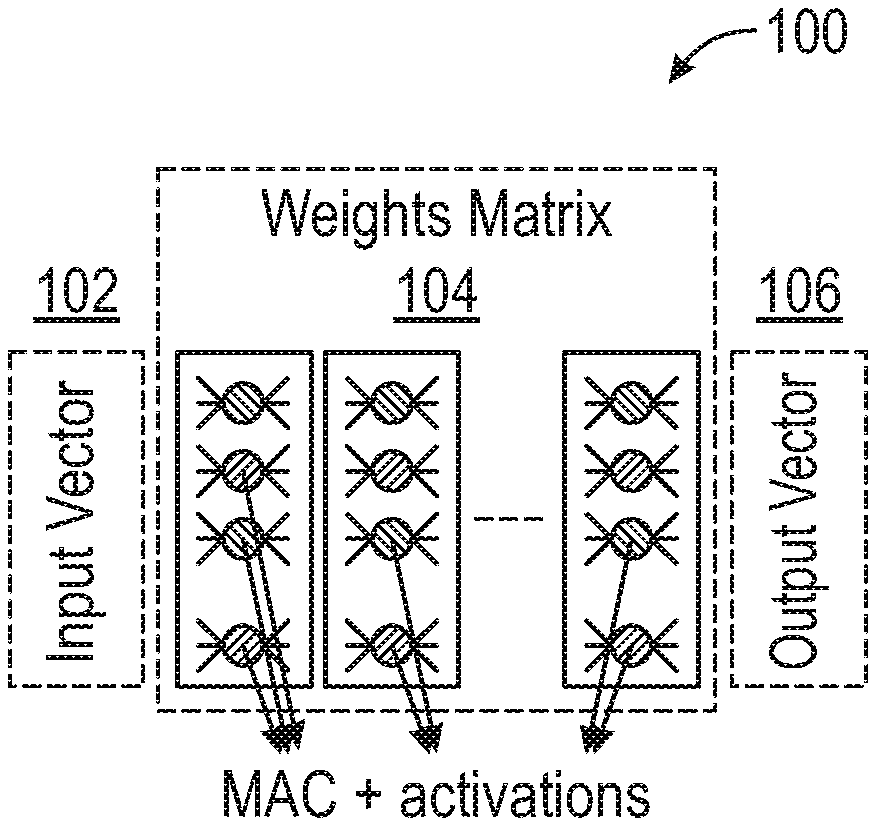
[0019] FIG. 1 depicts a high-level block diagram 100 of a multiplication-accumulation (MAC) operation that computes the product of two numbers and adds that product to an accumulator, in accordance with an embodiment of the disclosure.
a.rarw.a+(bc)(1) (Eq. 1)
[0020] The composition of a group of MACs may represent dot-products and vector-matrix multiplication. MAC operations are utilized in Machine Learning (ML) applications, and more specifically Deep Neural Networks (DNN). FIG. 1 represents a simple multi-layer fully connected neural network 100. Each of the neurons in the first layer computes the MAC between the input vector 102 and the corresponding weights in matrix 104. An activation function is applied to the partial result, and an output vector 106 is generated. This process takes place for every neuron present in a plurality of layers.
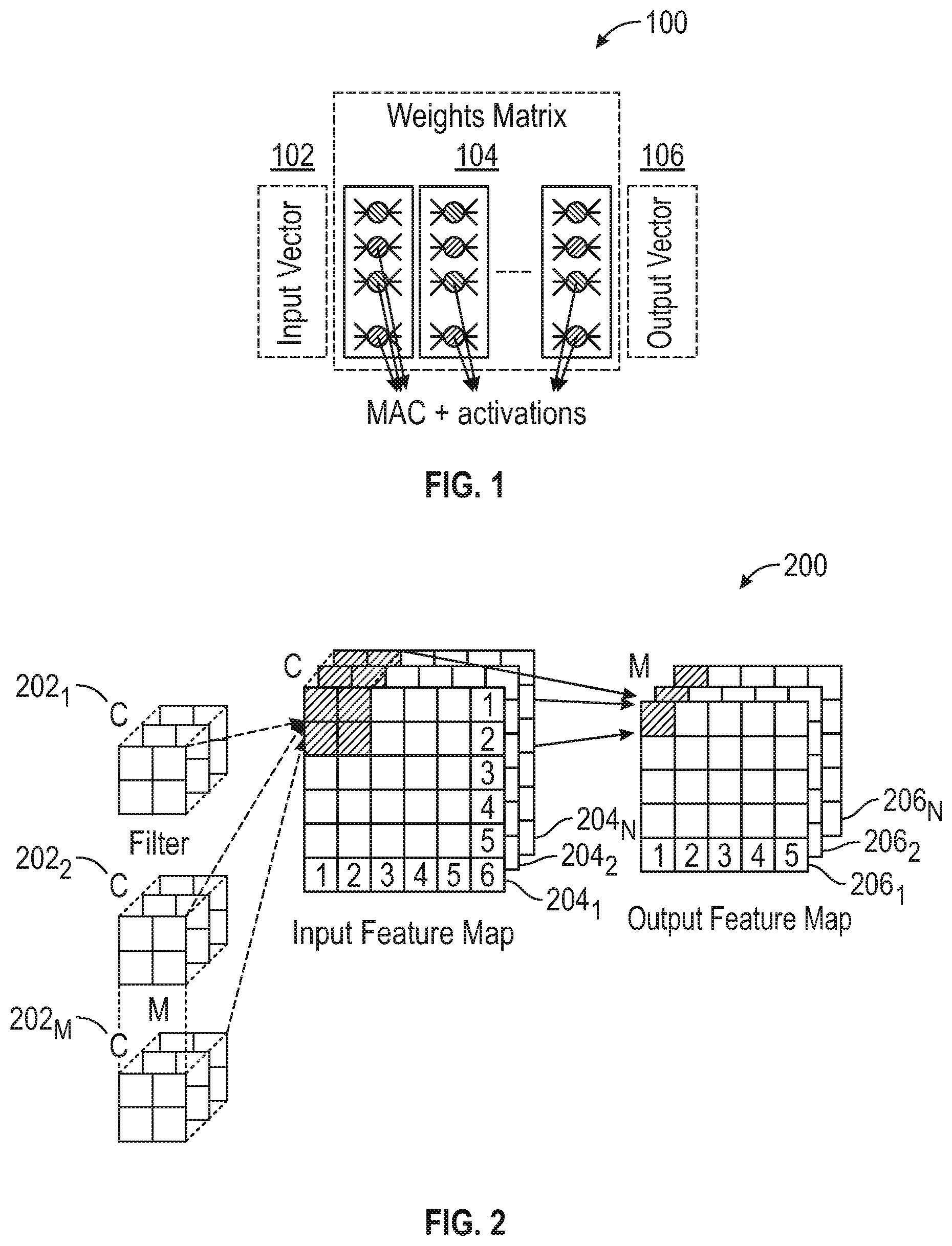
[0021] FIG. 2 depicts a convolution operation within a single-layer of a convolutional neural network (CNN 200), in accordance with an embodiment of the disclosure. Generally, the CNN 200 includes multiple "M" filters and multiple "C" input channels. A single filter is convolved across input feature maps in different channels to produce an output feature map corresponding to a single filter. Thus, there are multiple output feature maps each corresponding to an individual filter. Convolutional layers require the movement of large amounts of data, generate a significant computational load, and require buffers of considerable size to store intermediate values. In this example, there are multiple filters "M" 202.sub.1, 202.sub.2, . . . , 202.sub.M and multiple input channels. A single filter is convolved across "C" input feature maps 204.sub.1, 204.sub.2, and 204.sub.N in different channels to produce "M" output feature maps 206.sub.1, 206.sub.2, and 206.sub.N corresponding to a single filter. Thus, there are multiple output feature maps each corresponding to an individual filter. In the illustration of FIG. 2, it is assumed that the dimensions of the filters are 2.times.2 and the dimensions of the input feature map are 5.times.5. Thus, the total number of operations are 2.times.2.times.C.times.(5.times.5).times.M for the specific arrangement shown in FIG. 2.
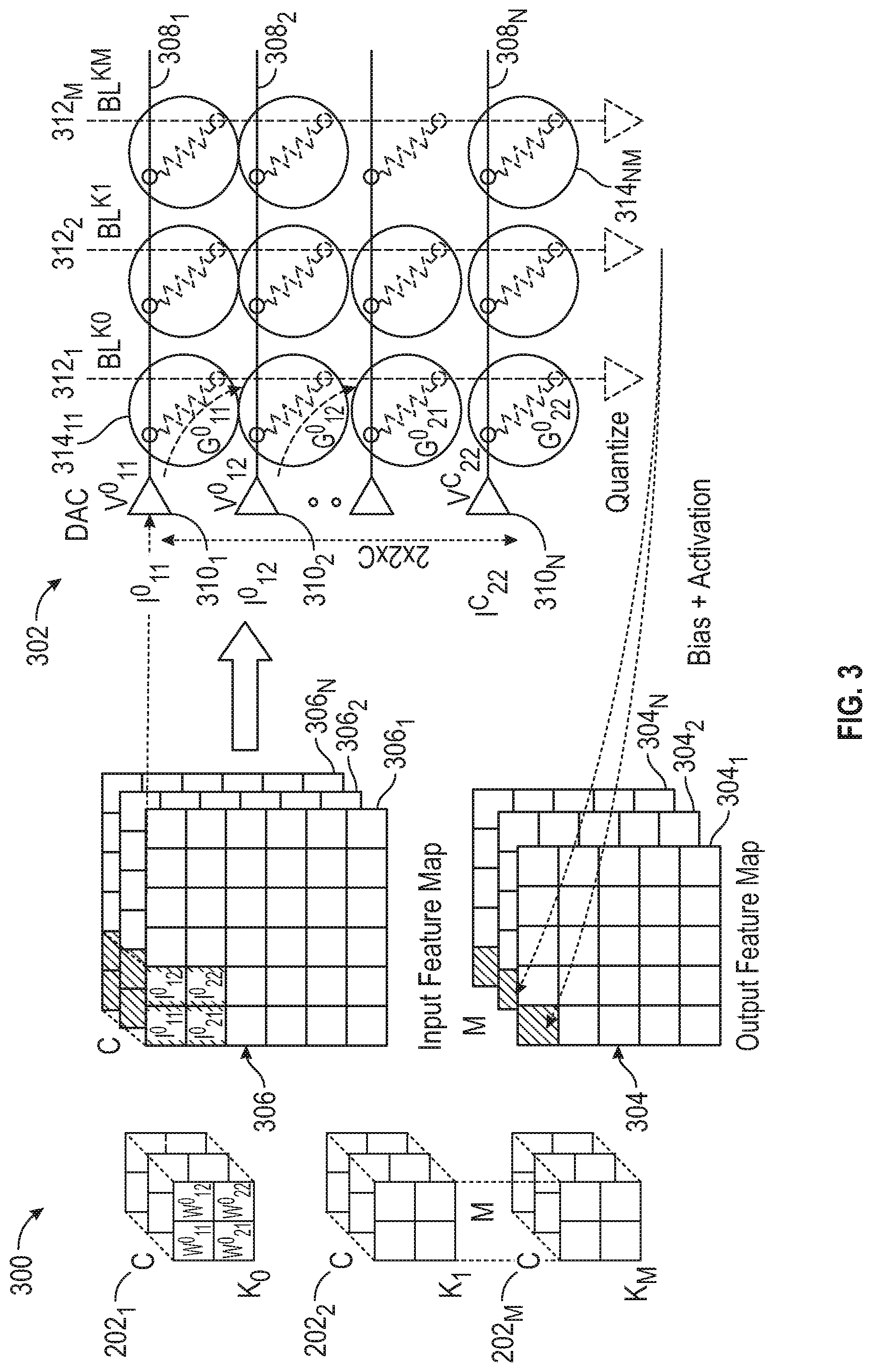
[0022] FIG. 3 depicts an architecture 300 showing how such an operation can be implemented using NVM crossbar 302, in accordance with an embodiment of the disclosure. Reference numerals identifying like components are repeated from FIG. 2. In NVM crossbar 302, weights for a convolutional filter are programmed into individual bit-cells W.sup.0.sub.11, W.sup.0.sub.12, W.sup.0.sub.21, W.sup.0.sub.22. The crossbar 302 includes a plurality of row signal lines 308.sub.1, 308.sub.2, . . . , 308.sub.N and column signal lines 312.sub.1, 312.sub.2, . . . , 312.sub.M. A plurality of neural network nodes are represented by 314.sub.11, . . . , 314.sub.NM, each of which includes a plurality of NVM elements which can be programmed between resistance states. It is generally useful to encode multiple linearly-separated resistance levels within an individual bit cell due to the wide separation between low-resistance state (LRS) R.sub.ON and the high-resistance state (HRS) R.sub.OFF. The LRS and HRS conductances are represented by G.sup.0.sub.11, G.sup.0.sub.12, G.sup.0.sub.21, G.sup.0.sub.22 . . . . In the case of correlated electron material RAM (CeRAM), the ratio of HRS/LRS is at least 2-orders of magnitude. Therefore, encoding a 4-bit (or 16 levels) resistance is possible. Digital words from the input feature maps 306.sub.1 . . . N are input to the crossbar 302 via corresponding inputs I.sup.0.sub.11, I.sup.0.sub.12, . . . , I.sup.C.sub.22 along the row signal lines 308.sub.11, 308.sub.12, . . . , 308.sub.22 of crossbar 302 and converted to analog-voltages V.sup.0.sub.11, V.sup.0.sub.12, . . . , V.sup.C.sub.22 using a digital-to-analog convertor (DAC), and applied across the NVM cell. The DAC includes converter elements 310.sub.1, 310.sub.2, . . . , 310.sub.N. The column signal lines 312.sub.1, 312.sub.2, . . . , 312.sub.M apply corresponding signals BL.sup.K0, BL.sup.K1, . . . , BL.sup.KM. The resultant current is therefore proportional to the dot-product of the input word and the weight. These individual currents are then accumulated in parallel on a bit line. Once the accumulated current signal develops on the bit line, it can then be digitized again using an analog-to-digital converter (ADC) and bias-addition, scaling and activation-functions can be applied on the resulting digital word to obtain output activation. The bias+activation may be represented by:
BL.sup.K.sup.0=.SIGMA..sub.c-1.sup.c[(G.sup.0.sub.11*Vc.sub.11+ . . . +G.sup.0.sub.22*Vc.sub.22)] (Eq. 2)
[0023] In FIG. 3, a mapping of CNN to NVM crossbars with M filters and C input channels is depicted. In certain embodiments, it is assumed that the weights co are stationary i.e., they are programmed into the crossbar once and do not change during the course of inference operations. Typical NVM elements (for instance, Phase-Change Memory and Resistive RAM) have a limited write "endurance"--i.e., it is possible to write to them a limited number of times (say, approximately 10.sup.8 times) after which the devices exhibit functional failure. Other NVM elements (such as Magnetic RAM and CeRAM) demonstrate the promise for relatively higher endurance (near 10.sup.12), but continuous operation still leads to a limited lifetime. Hence, such lifetime limits pose significant constraints on accelerator architectures that rely upon updating weights on a per-inference cycle. For example, for an IoT-class accelerator operating at 100 MHz, an accelerator with an endurance of 10.sup.8 has a lifetime of 1-sec, and an accelerator with an endurance of 10.sup.12 has a lifetime of 10,000 secs or 4-days (worst-case, peak usage). Therefore, such weights cannot be practically streamed from an external DRAM and must be fixed on-chip. Further, NVM bit cells suffer from high write-powers, and consequent expensive power consumption to perform update operations. Thus, the write phase can be problematic and take a long time to complete.
[0024] Such arrangements differ from SRAM behavior (which has significantly higher write endurance) and are not amenable to reprogramming the weights during inference. As a consequence, the entire network needs to be unrolled into an on-chip crossbar and fixed during inference. While this has the advantage of eliminating DRAM power consumption, it undesirably limits the maximum size of the network that can be programmed on-chip. Further, it also incurs an area penalty as mapping larger networks requires instantiation of crossbars that are megabits in capacity. This consumes higher area and increases susceptibility to chip-failures due to yield loss. Moreover, instantiating multiple crossbars requires instantiation of multiple ADCs/DACs, all of which need to be programmed, trimmed and compensated for drift.
[0025] An NVM/CeRAM element is a particular type of random access memory formed (wholly or in part) from a correlated electron material. The CeRAM may exhibit an abrupt conductive or insulative state transition arising from electron correlations rather than solid state structural phase changes such as, for example, filamentary formation and conduction in resistive RAM devices. An abrupt conductor/insulator transition in a CeRAM may be responsive to a quantum mechanical phenomenon, in contrast to melting/solidification or filament formation.
[0026] A quantum mechanical transition of a CeRAM between an insulative state and a conductive state may be understood in terms of a Mott transition. In a Mott transition, a material may switch from an insulative state to a conductive state if a Mott transition condition occurs. When a critical carrier concentration is achieved such that a Mott criteria is met, the Mott transition will occur and the state will change from high resistance/impedance (or capacitance) to low resistance/impedance (or capacitance).
[0027] A "state" or "memory state" of the CeRAM element may be dependent on the impedance state or conductive state of the CeRAM element. In this context, the "state" or "memory state" means a detectable state of a memory device that is indicative of a value, symbol, parameter or condition, just to provide a few examples. In a particular implementation, a memory state of a memory device may be detected based, at least in part, on a signal detected on terminals of the memory device in a read operation. In another implementation, a memory device may be placed in a particular memory state to represent or store a particular value, symbol or parameter by application of one or more signals across terminals of the memory device in a "write operation."
[0028] A CeRAM element may comprise material sandwiched between conductive terminals. By applying a specific voltage and current between the terminals, the material may transition between the aforementioned conductive and insulative states. The material of a CeRAM element sandwiched between conductive terminals may be placed in an insulative state by application of a first programming signal across the terminals having a reset voltage and reset current at a reset current density, or placed in a conductive state by application of a second programming signal across the terminals having a set voltage and set current at set current density.
[0029] In accordance with embodiments of the disclosure, a vector-matrix multiplication performs the following MAC operations, where an Input vector V={v.sub.i}, i.di-elect cons.[0, M-1], matrix W={w.sub.ij}, j.di-elect cons.[0, N-1], and an output vector O is composed of:
O.sub.j=.SIGMA..sub.iw.sub.ija.sub.i (Eq. 3)
[0030] The NVM equivalent is represented by:
I.sub.j=.SIGMA..sub.iwg.sub.ijv.sub.i (Eq. 4)
[0031] where matrix I represents the currents flowing through the bitlines, and V is the input voltages vector and g is the conductance of the NVM elements. For a K-bit weight representation, there can only be 2.sup.K unique weight values. For low-precision weight encoding (3 or 4-bit values), this leads to only 8 or 16 such unique weight values:
g.sub.ij=.SIGMA..sub.k=0.sup.K-1g'.sub.ijk(R.sub.ON+.DELTA.k) (Eq. 5)
[0032] where g'.sub.ijk.di-elect cons.{0,1}, k.di-elect cons.[0, K-1] and .DELTA.=(R.sub.OFF-R.sub.ON)/2.sup.K.
[0033] Voltages V'={v'.sub.i} are defined as following:
v i ' = { 0 , v i ( Eq . 6 ) ##EQU00001##
[0034] where v'.sub.i=0 if activation a.sub.i does not have g.sub.ijk as a multiplicand, otherwise where v'.sub.i=v.sub.i, Eq. 5 can be rewritten as:
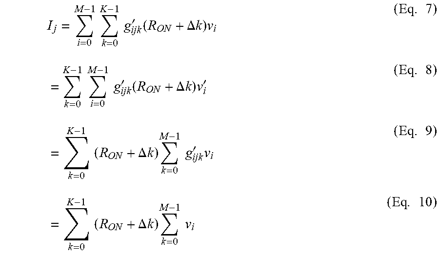
I j = i = 0 M - 1 k = 0 K - 1 g ijk ' ( R ON + .DELTA. k ) v i ( Eq . 7 ) = k = 0 K - 1 i = 0 M - 1 g ijk ' ( R ON + .DELTA. k ) v i ' ( Eq . 8 ) = k = 0 K - 1 ( R ON + .DELTA. k ) k = 0 M - 1 g ijk ' v i ( Eq . 9 ) = k = 0 K - 1 ( R ON + .DELTA. k ) k = 0 M - 1 v i ( Eq . 10 ) ##EQU00002##
[0035] given that g'.sub.ijk=0 should be v'.sub.i=0.
[0036] Refactoring as represented by Eq. 10 leads to a simpler implementation where all input multiplicands are initially added to conditionally add together the input activations depending on whether they factor into the MAC operation with a specific weight value. The initial addition operation can be done using NVM elements. However, in accordance with embodiments of the disclosure, these NVM elements need not be precisely programmed. A binary weight encoding (R.sub.ON/R.sub.OFF) is utilized to connect an input activation to a weight value without need for precision programming.
[0037] FIG. 4 depicts a schematic of a K-bit precision architecture 400 for implementing refactored matrix multiplication, in accordance with an embodiment of the disclosure. In accordance with an embodiment, the refactored matrix G can be deployed in a system composed of block 402 of M digital-to-analog converters (DACs) 403.sub.1, . . . , 403.sub.M, an M.times.N.times.K crossbar 404 and a multiplier/scaling module 406. The crossbar 404 includes a plurality of neural network nodes 408.sub.11, . . . , 408.sub.MN, provided at each junction of row signal lines 410.sub.1, 410.sub.2, 410.sub.3, . . . , 410.sub.M and column signal lines 412.sub.1, 412.sub.2, 412.sub.3, . . . , 412.sub.N as shown. Each respective node 408.sub.11, . . . , 408.sub.M,N includes one or more NVM elements to store the weights associated with that node. As described above, a node is switchable between a first impedance state and a second impedance state (R.sub.ON/R.sub.OFF). The multiplier/scaling module 406 includes nodes 407.sub.0, . . . , 407.sub.K-1 corresponding to weights w_0, w_1, w_K-1. Input activations a_0, a 1, . . . , a_M-1 along respective row signal lines 410.sub.1, 410.sub.2, 410.sub.3, . . . , 410.sub.M are first summed together in the crossbar 404 by placing the nodes 408.sub.11, . . . , 408.sub.MN into R.sub.ON/R.sub.OFF states as described above where the NVM elements do not require precision programming. In the example illustrated in FIG. 4, certain nodes among the plurality of nodes 408.sub.1,1, . . . , 408.sub.MN are switched between impedance states as shown. A summed signal from each column Nis input to a respective node 407.sub.0, . . . , 407.sub.K-1 of the multiplier scaling module 406, and the final MAC computation occurs in a single column in the multiplier/scaling module 406 where all elements are precisely programmed (K in elements in total).
[0038] FIG. 5 depicts a flow-diagram 500 of a non-precision programming process for performing multiply-accumulate acceleration, in accordance with an embodiment of the disclosure. For an M.times.N crossbar having K-bit weights, M.times.N.times.2.sup.K elements are binary programmed and 2.sup.K.times.N elements are precision programmed. The output is given by:
output.sub.j=sum(g.sub.ijk)sum(v'.sub.ik) (Eq. 11)
where K provides 2.sup.K levels. In block 502, the process is initialized and proceeds to block 504 of the low-precision write loop. In block 504 ijk are updated. In block 506 the g_ijk (binary) resistance is read. Then in block 508, g_ijk (binary) resistance is written. The process terminates at block 510. In this implementation, the M.times.N.times.2.sup.K cells are programmed to either a "0" (R.sub.OFF) or a "1" (R.sub.ON) where 2.sup.K defines the number of levels. From here, 2.sup.K.times.N<<M.times.N non-volatile memory cells are precision programmed.
[0039] FIG. 6 depicts a flow diagram 600 of a precision programming process of the 2.sup.K.times.N non-volatile memory cells, in accordance with an embodiment of the disclosure. The process is initialized at block 602 and proceeds to block 604 of a high-precision write loop. In block 604, ij are updated. Next, in block 606 g_ij are read (non-binary). A high-precision operation changes the resistivity of a single non-volatile memory cell to a very precise known value between 2{circumflex over ( )}4 possible conductances. In block 608, the multilevel resistance g_ij is tuned. Then, in block 610, the multilevel resistance g_ij is read, and the correct multilevel resistance verified in block 612. The process loops back to block 604 if the multilevel resistance is correct, otherwise, the process proceeds back to block 608 for further tuning. The process terminates at block 614. The output is given by:
output.sub.j=sum(v_i*g_ij) (Eq. 12)
[0040] where v_i, g_ij are high precision numbers in K levels.
[0041] FIG. 7 depicts a flow-diagram 700 of a method for performing multiply-accumulate acceleration in a neural network (100, FIG. 1), in accordance with an embodiment of the disclosure. The method is initialized at block 702, and proceeds to block 704 which corresponds to the low-precision write loop 500 shown in FIG. 5. In the low precision write loop 500, the input activations a_0, a_1, . . . , a_M-1 are applied to a summing array (crossbar 404, FIG. 4). A summed signal is generated by each column of NVM elements in the summing array as shown in FIG. 4 by the low-precision write loop 500. The process proceeds to block 706, which corresponds to the high-precision write loop 600 shown in FIG. 6. In the high-precision write loop 600, the summed signal is input to a multiplying array (module 406, FIG. 4) having a plurality of NVM elements. In block 706, each NVM element in the multiplying array is precisely programmed to a conductance level proportional to a weight in the neural network as shown in the flow diagram of FIG. 6. The process terminates at block 708.
[0042] Reference in the specification to "one embodiment" or "an embodiment" means that a particular feature, structure, or characteristic described in connection with the embodiment is included in at least one embodiment of the system. The appearances of the phrase "in one embodiment" in various places in the specification are not necessarily all referring to the same embodiment.
[0043] Embodiments of the present disclosure are described herein with reference to flowchart illustrations and/or block diagrams of methods, apparatus (systems), and computer program products according to embodiments of the disclosure. It will be understood that each block of the flowchart illustrations and/or block diagrams, and combinations of blocks in the flowchart illustrations and/or block diagrams, can be implemented by computer readable program instructions.
[0044] Some portions of the detailed descriptions, like the processes may be presented in terms of algorithms and symbolic representations of operations on data bits within a computer memory. An algorithm may be generally conceived to be steps leading to a desired result. The steps are those requiring physical transformations or manipulations of physical quantities. Usually, though not necessarily, these quantities take the form of electrical or magnetic signals capable of being stored, transferred, combined, compared, and otherwise manipulated. It has proven convenient at times, principally for reasons of common usage, to refer to these signals as bits, values, elements, symbols, characters, terms, numbers, or the like.
[0045] It should be borne in mind, however, that all of these and similar terms are to be associated with the appropriate physical quantities and are merely convenient labels applied to these quantities. Unless specifically stated otherwise as apparent from the following discussion, it is appreciated that throughout the description, discussions utilizing terms such as "processing" or "computing" or "calculating" or "determining" or "deriving" or "displaying" or the like, refer to the action and processes of a computer system, or similar electronic computing device, that manipulates and transforms data represented as physical (electronic) quantities within the computer system's registers and memories into other data similarly represented as physical quantities within the computer system memories or registers or other such information storage, transmission or display devices.
[0046] The operations described herein can be performed by an apparatus. This apparatus may be specially constructed for the required purposes, or it may comprise a general-purpose computer selectively activated or reconfigured by a computer program stored in the computer. Such a computer program may be stored in a computer readable storage medium, such as, but is not limited to, any type of disk, read-only memories (ROMs), random access memories (RAMs), EPROMs, EEPROMs, magnetic or optical cards, or any type of media suitable for storing electronic instructions. A computer readable storage medium, as used herein, is not to be construed as being transitory signals per se, such as radio waves or other freely propagating electromagnetic waves, electromagnetic waves propagating through a waveguide or other transmission media (e.g., light pulses passing through a fiber-optic cable), or electrical signals transmitted through a wire.
[0047] Accordingly, embodiments and features of the present disclosure include, but are not limited to, the following combinable embodiments.
[0048] In one embodiment, a method of performing multiply-accumulate acceleration in a neural network includes generating, in a summing array having a plurality of non-volatile memory elements arranged in columns, a summed signal by the columns of non-volatile memory elements in the summing array, each non-volatile memory element in the summing array being programmed to either a high or low resistance state; and inputting the summed signal from the summing array to a multiplying array having a plurality of non-volatile memory elements, each non-volatile memory element in the multiplying array being precisely programmed to a conductance level proportional to a weight in the neural network.
[0049] In another embodiment, the summing array and multiplying array is an M.times.N crossbar having K-bit weights, where M.times.N.times.2{circumflex over ( )}Kelements are programmed to either the high or low resistance state and 2.times.K.times.N elements are precisely programmed to the conductance level proportional to the weight in the neural network.
[0050] In another embodiment, a plurality of input activations are conditionally summed depending upon specific weight values.
[0051] In another embodiment, a plurality of input activations are significantly greater than a plurality of weight values.
[0052] In another embodiment, summing array comprises a plurality of high and low resistance levels.
[0053] In another embodiment, the method further comprises the M.times.N.times.2{circumflex over ( )}K elements programmed to either a resistance "off" state or a resistance "on" state for 2{circumflex over ( )}K levels.
[0054] In another embodiment, 2{circumflex over ( )}K.times.N<<M.times.N non-volatile memory cells are fine-tuned.
[0055] In another embodiment, the method further comprises scaling an output in a multiplier/scaling module.
[0056] In a further embodiment, an architecture for performing multiply-accumulate operations in a neural network includes a summing array having a plurality of non-volatile memory elements arranged in columns, the summing array generating a summed signal by the columns of non-volatile memory elements in the summing array, each non-volatile memory element in the summing array being programmed to either a high or low resistance state; and a multiplying array having a plurality of non-volatile memory elements that receive a summed signal from the summing array, each non-volatile memory element in the multiplying array being precisely programmed to a conductance level proportional to a weight in the neural network.
[0057] In another embodiment, the summing array and multiplying array is an M.times.N crossbar having K-bit weights, where M.times.N.times.2{circumflex over ( )}Kelements are programmed to either the high or low resistance state and 2{circumflex over ( )}K.times.N elements are precisely programmed to the conductance level proportional to the weight in the neural network.
[0058] In another embodiment, a plurality of input activations is conditionally summed depending upon specific weight values.
[0059] In another embodiment, a plurality of input activations is significantly greater than a plurality of weight values.
[0060] In another embodiment, the architecture further comprises a plurality of resistors and where the summing array comprises a plurality of high and low resistance levels.
[0061] In another embodiment, the architecture further comprises the M.times.N.times.2{circumflex over ( )}K elements programmed to either a resistance "off" state or a resistance "on" state for 2{circumflex over ( )}K levels.
[0062] In another embodiment, 2{circumflex over ( )}K.times.N<<M.times.N non-volatile memory cells are fine-tuned.
[0063] In another embodiment, the architecture further comprises a multiplier/scaling module for scaling an output.
[0064] In another further embodiment, an architecture for performing multiply-accumulate operations in a neural network includes a crossbar including a plurality of crossbar nodes arranged in an array of rows and columns, each crossbar node being programmable to a first resistance level or a second resistance level, the crossbar being configured to sum a plurality of analog input activation signals over each column of crossbar nodes and output a plurality of summed activation signals; and a multiplier, coupled to the crossbar, including a plurality of multiplier nodes, each multiplier node being programmable to a resistance level proportional to one of a plurality of neural network weights, the multiplier being configured to sum the plurality of summed activation signals over the multiplier nodes and output an analog output activation signal.
[0065] In another embodiment, each crossbar node includes one or more non-volatile elements (NVMs), and each multiplier node includes a plurality of NVMs.
[0066] In another embodiment, the crossbar includes M rows, N columns, K-bit weights and M.times.N.times.2K programmable NVMs, and the multiplier includes N multiplier nodes and N.times.2K programmable NVMs.
[0067] In another embodiment, the architecture further comprises a plurality of digital-to-analog converters (DACs) coupled to the crossbar, each DAC being configured to receive a plurality of digital input activation signals and output the plurality of analog input activation signals.
[0068] In accordance with the foregoing, a method and architecture for performing multiply-accumulate acceleration is disclosed. Having thus described the disclosure of the present application in detail and by reference to embodiments thereof, it will be apparent that modifications and variations are possible without departing from the scope defined in the appended claims as follows:
* * * * *
D00000
D00001
D00002
D00003
D00004
D00005
XML
uspto.report is an independent third-party trademark research tool that is not affiliated, endorsed, or sponsored by the United States Patent and Trademark Office (USPTO) or any other governmental organization. The information provided by uspto.report is based on publicly available data at the time of writing and is intended for informational purposes only.
While we strive to provide accurate and up-to-date information, we do not guarantee the accuracy, completeness, reliability, or suitability of the information displayed on this site. The use of this site is at your own risk. Any reliance you place on such information is therefore strictly at your own risk.
All official trademark data, including owner information, should be verified by visiting the official USPTO website at www.uspto.gov. This site is not intended to replace professional legal advice and should not be used as a substitute for consulting with a legal professional who is knowledgeable about trademark law.