Method For Forming A Structure With A Hole
Pierreux; Dieter ; et al.
U.S. patent application number 16/995281 was filed with the patent office on 2021-02-25 for method for forming a structure with a hole. The applicant listed for this patent is ASM IP Holding B.V.. Invention is credited to Bert Jongbloed, Dieter Pierreux, Steven van Aerde.
| Application Number | 20210057275 16/995281 |
| Document ID | / |
| Family ID | 1000005048766 |
| Filed Date | 2021-02-25 |


| United States Patent Application | 20210057275 |
| Kind Code | A1 |
| Pierreux; Dieter ; et al. | February 25, 2021 |
METHOD FOR FORMING A STRUCTURE WITH A HOLE
Abstract
A method for forming a structure with a hole on a substrate is disclosed. The method may comprise: depositing a first structure on the substrate; etching a first part of the hole in the first structure; depositing a plug fill in the first part of the hole; depositing a second structure on top of the first structure; etching a second part of the hole substantially aligned with the first part of the hole in the second structure; and, etching the plug fill of the first part of the hole and thereby opening up the hole by dry etching. In this way 3-D NAND device may be provided.
| Inventors: | Pierreux; Dieter; (Dilbeek, BE) ; van Aerde; Steven; (Tielt-Winge, BE) ; Jongbloed; Bert; (Oud-Heverlee, BE) | ||||||||||
| Applicant: |
|
||||||||||
|---|---|---|---|---|---|---|---|---|---|---|---|
| Family ID: | 1000005048766 | ||||||||||
| Appl. No.: | 16/995281 | ||||||||||
| Filed: | August 17, 2020 |
Related U.S. Patent Documents
| Application Number | Filing Date | Patent Number | ||
|---|---|---|---|---|
| 62890288 | Aug 22, 2019 | |||
| Current U.S. Class: | 1/1 |
| Current CPC Class: | H01L 21/76879 20130101; G11C 5/025 20130101; H01L 27/11582 20130101; H01L 21/76802 20130101; H01L 27/11556 20130101; H01L 23/5384 20130101; G11C 5/06 20130101 |
| International Class: | H01L 21/768 20060101 H01L021/768; H01L 27/11556 20060101 H01L027/11556; H01L 27/11582 20060101 H01L027/11582; G11C 5/02 20060101 G11C005/02; G11C 5/06 20060101 G11C005/06; H01L 23/538 20060101 H01L023/538 |
Claims
1. A method of forming a structure with a hole on a substrate, the method comprising: depositing a first structure on the substrate; etching a first part of the hole in the first structure; depositing a plug fill in the first part of the hole; depositing a second structure on top of the first structure; etching a second part of the hole substantially aligned with the first part of the hole in the second structure; and, etching the plug fill of the first part of the hole and thereby opening up the hole, wherein etching the plug fill comprises dry etching.
2. The method of claim 1, wherein etching the plug fill comprises providing the substrate to a reaction chamber constructed and arranged to provide a gaseous etchant for isotropic etching the plug fill in the reaction chamber.
3. The method of claim 2, wherein etching the plug fill comprises providing one or more of the gaseous etchants comprising a halide to the reaction chamber.
4. The method of claim 3, wherein the halide is selected from the group consisting of nitrogen trifluoride (NF.sub.3) and chlorine (Cl.sub.2) for thermally activated etching the plug.
5. The method of claim 2, wherein during etching the plug fill the temperature in the reaction chamber is below 500.degree. C. and the pressure in the reactor is below 1 Torr and the reaction chamber is substantially radical and/or ion free.
6. The method of claim 2, wherein the halide is selected from boron chloride (BCl.sub.3); fluorine (F.sub.2), fluoroform (CHF.sub.3), sulfur hexafluoride (SF.sub.6), tetrafluoromethane (CF.sub.4) in the reaction chamber for dry etching the plug.
7. The method according to claim 1, wherein the method comprises loading the substrate to a boat and moving the boat with substrates to a batch reactor of a vertical furnace for processing.
8. The method according to claim 1, wherein depositing the plug fill comprises providing a germanium precursor.
9. The method according to claim 8 wherein the germanium precursor comprise a precursor selected from the group consisting of germane, digermane, dichlorogermane, trichlorogermane, tetrachlorogermane, germanium alkoxide, and any combination thereof.
10. The method according to claim 8, wherein depositing the plug fill comprises providing a silicon precursor and the plug fill comprises silicon germanium (SiGe) with a germanium content from 1% to 100%.
11. The method according to claim 10, wherein the silicon precursor comprising a precursor selected from the group consisting of silane, disilane, trisilane, chlorosilane, dichlorosilane, trichlorosilane, tetrachlorosilane, methylsilane, dimethylsilane, trimethylsilane, tetramethylsilane, and any combination thereof.
12. The method according to claim 10, wherein a ratio of germanium to silicon is increased during depositing the silicon germanium to increase the germanium content in the silicon germanium from a first layer of the plug towards the center and top of the plug.
13. The method according to claim 1, wherein depositing the plug fill comprises deposition steps with at least one etch step.
14. The method according to claim 1, wherein the method comprises: depositing a first liner on top of the first structure and in the first part of the hole before depositing a plug fill in the first part of the hole.
15. The method according to claim 14, wherein the first liner comprises silicon, silicon oxide and/or germanium oxide.
16. The method according to claim 14, wherein depositing the first liner comprises providing a germanium precursor and the germanium precursor is selected from germane, digermane, dichlorogermane, trichlorogermane, tetrachlorogermane, germanium alkoxide, or a combination thereof.
17. The method according to claim 14, wherein depositing the first liner comprises providing a silicon precursor wherein the silicon precursor comprises silane, disilane, trisilane, chlorosilane, dichlorosilane, trichlorosilane, tetrachlorosilane, methylsilane, dimethylsilane, trimethylsilane, tetramethylsilane, or any combination thereof.
18. The method according to claim 1, wherein the method comprises: depositing a second liner on top of the second structure and in the second part of the hole, etching the bottom of the second part of the hole and etching the plug fill of the first part of the hole.
19. The method according to claim 18, wherein the second liner comprises silicon, an oxide, a nitride and/or a carbide.
20. The method according to claim 19, wherein the second liner comprises silicon oxy carbide nitride (SiOCN), aluminum nitride and/or boron carbide.
21. The method according to claim 20, wherein depositing the second liner comprises providing a nitrogen or oxide comprising reactant.
22. The method according to claim 14, wherein depositing the first or second liner comprises depositing a liner with a thickness smaller than 10 nanometer.
23. The method according to claim 14 wherein the method comprises removing the first and/or second liner with a dry etch.
24. The method of claim 23, wherein the method comprises providing the substrate to a reaction chamber constructed and arranged to provide a gaseous etchant for isotropic etching the first and/or second liner.
25. The method of claim 24, wherein the method comprises providing one or more of the gaseous etchants comprising a halide to the reaction chamber.
26. The method of claim 25 wherein the halide is selected from nitrogen trifluoride NF.sub.3 and chlorine Cl.sub.2, in the reaction chamber for dry etching the plug.
27. The method of claim 24, wherein the temperature in the reaction chamber is below 500.degree. C. and the pressure in the reaction chamber is below 1 Torr and the reaction chamber is substantially radical and/or ion free.
28. The method of claim 1, wherein etching the first or second part of the hole in the first or second structure comprises anisotropic etching.
29. The method of claim 1, wherein the method comprises polishing the plug fill before depositing the second structure on top of the first structure.
30. The method of claim 1, wherein any of the above steps are repeated to form a 3-D NAND device.
31. The method of claim 1, wherein depositing a first or second structure on the substrate comprising depositing a bilayer structure on the substrate, the bilayer structure comprising alternating layers of a silicon oxide layer and a silicon nitride layer.
32. The method according to claim 1, wherein the opening of the hole in the structure has a width smaller than 200 nm.
Description
CROSS-REFERENCE TO RELATED APPLICATIONS
[0001] This application claims priority to U.S. Provisional Patent Application Ser. No. 62/890,288 filed Aug. 22, 2019 titled METHOD FOR FORMING A STRUCTURE WITH A HOLE, the disclosure of which is hereby incorporated by reference in its entirety.
FIELD OF INVENTION
[0002] The present disclosure generally relates to a method for forming a structure with a hole on a substrate. The method may include deposition of a sacrificial material and etching the material to achieve proper formation of device structures for a 3-D NAND device.
BACKGROUND OF THE DISCLOSURE
[0003] NAND devices are logic gates usable in applications such as flash memory, for example. Manufacture of the 3D NAND devices may include formation of a hole in a structure disposed on a substrate. The hole may be produced by making a first part of the hole in a first structure which first part of the hole then may be filled with a sacrificial material. On top of the first structure a second structure may be provided and a second part of the hole which is aligned with the first part of the hole may be provided. The hole may then be created by removing the sacrificial material from the first part of the hole via the second part of the hole.
[0004] An example of such a process for manufacturing a 3D NAND device may be illustrated in FIGS. 1A-1D. An intermediate product 100 for a 3D NAND device may be manufactured by a using a substrate 110 provided with a structure, for example a bilayer comprising a nitride layer 120 and an oxide layer 130. Deposition of the nitride layer 120 and the oxide layer 130 may be repeated as needed to form a structure. As shown in FIG. 1A a first structure e.g. a first stack 140 comprising alternating nitride 120 and oxide layers 130 may be provided. Also a second structure e.g. a second stack 150 comprising alternating nitride 120 and oxide layers 130 may be provided.
[0005] The nitride layers 120 and the oxide layers 130 undergo a dry etch process to form a first part of a hole in the structure, as shown in FIG. 1B. FIG. 1C illustrates the intermediate product 100 for the NAND device after the dry etch and after undergoing a first process to form a liner, a second process to form a plug fill, and a third process to polish the surface. The first part of the hole 100 then comprises a liner 160 and a plug fill 170. The liner 160 may comprise silicon oxide (SiO.sub.x), for example. After the third polishing process, additional oxide-nitride layer stacks may be added on top of the stack 150, the liner 160, and the plug fill 170.
[0006] However, it may come to a point that after the first part of the hole is filled with the liner 160 and the plug fill 170, the liner 160 and the plug fill 170 have to be removed. The plug fill 170 may be removed with a wet etch process. A wet clean process may follow to remove the liner (160). Due to capillary effects in the hole wet good etching of the plug fill may be difficult to achieve.
[0007] FIG. 1D illustrates the intermediate product 100 after removal took place. However, the chemistries may leave a residue 180 and cause damage 190 to either the nitride layer 120 and/or the oxide layer 130 by the chemistries used for the removal of liner 160 or plug fill 170. The residue 180 and the damage 190 may render the NAND device unusable. Since the holes may become deeper and narrower with the next technology nodes it may be expected that the capillary effects of the wet etch liquid in the holes may increase and therefore good quality etching may be more difficult to achieve. In addition, the removal of the liner 160 and the plug fill 170 may be done with a slow etch rate, which means that the time to remove the liner 160 and the plug fill 170 may be undesirably long.
[0008] As a result, it is desired to achieve an improved apparatus and method for forming a structure with a hole on a substrate.
SUMMARY OF THE DISCLOSURE
[0009] This summary is provided to introduce a selection of concepts in a simplified form. These concepts are described in further detail in the detailed description of example embodiments of the disclosure below. This summary is not intended to identify key features or essential features of the claimed subject matter, nor is it intended to be used to limit the scope of the claimed subject matter.
[0010] In accordance with at least one embodiment of the invention, a method is disclosed. An exemplary method comprises a method of forming a structure with a hole on a substrate. The method may be for forming a 3-D NAND device. The method of forming a structure with a hole on a substrate may comprise depositing a first structure on the substrate, etching a first part of the hole in the first structure and depositing a plug fill in the first part of the hole. Subsequently, the method may continue by depositing a second structure on top of the first structure, etching a second part of the hole substantially aligned with the first part of the hole in the second structure; and, etching the plug fill of the first part of the hole and thereby opening up the hole. Etching the plug fill may comprise dry etching.
[0011] These and other embodiments will become readily apparent to those skilled in the art from the following detailed description of certain embodiments having reference to the attached figures, the invention not being limited to any particular embodiment(s) disclosed.
BRIEF DESCRIPTION OF THE DRAWING FIGURES
[0012] These and other features, aspects, and advantages of the invention disclosed herein are described below with reference to the drawings of certain embodiments, which are intended to illustrate and not to limit the invention.
[0013] FIGS. 1A-1D are cross-sectional illustrations of intermediate products for a prior art process for forming a NAND device.
[0014] FIGS. 2A-2J are cross-sectional illustrations of an intermediate product for a NAND device formed in accordance with at least one embodiment.
[0015] FIG. 3 is a process flow diagram in accordance with the embodiment.
[0016] FIG. 4 is a cross-sectional illustration of a NAND device formed in accordance with the embodiment.
[0017] It will be appreciated that elements in the figures are illustrated for simplicity and clarity and have not necessarily been drawn to scale. For example, the dimensions of some of the elements in the figures may be exaggerated relative to other elements to help improve understanding of illustrated embodiments of the present disclosure.
DETAILED DESCRIPTION OF EXEMPLARY EMBODIMENTS
[0018] Although certain embodiments and examples are disclosed below, it will be understood by those in the art that the invention extends beyond the specifically disclosed embodiments and/or uses of the invention and obvious modifications and equivalents thereof. Thus, it is intended that the scope of the invention disclosed should not be limited by the particular disclosed embodiments described below.
[0019] The illustrations presented herein are not meant to be actual views of any particular material, structure, or device, but are merely idealized representations that are used to describe embodiments of the disclosure.
[0020] Three-dimensional (3-D) Not-AND (NAND) devices may be utilized in memory applications. The manufacturing of 3-D NAND devices may comprise intermediate product structures comprising stacks of bilayers disposed on each other. The bilayers may comprise oxides and nitrides, for example. When disposing stacks of multiple bilayers on other stacks, alignment and stresses on the layers and different features may become critical.
[0021] FIG. 2A illustrates an intermediate product 200 for a 3-D NAND device in accordance with at least one embodiment. The intermediate product 200 may comprise a substrate 210 and a first structure e.g. a first bilayer stack comprising a nitride layer 220 and an oxide layer 230. The substrate 210 may comprise silicon, silicon oxide, or a metal oxide. The nitride layer 220 may comprise at least one of: silicon nitride, germanium nitride, silicon germanium nitride (SiGeN), silicon oxynitride (SiON), germanium oxynitride (GeON), or combinations thereof. The oxide layer 230 may comprise at least one of: silicon oxide, germanium oxide, silicon germanium oxide (SiGeOx), germanium oxynitride (GeON), silicon oxynitride (SiON), or combinations thereof. The deposition of the nitride layer 220 and the oxide layer 230 may be done in batch in a reaction chamber of a vertical furnace. The method may therefore comprise loading the substrate to a boat and moving the boat with substrates to a reaction chamber of a batch reactor of a vertical furnace for processing.
[0022] The intermediate product 200 then may go through a dry etch process to create a first part of a hole in the first structure of the product 200 as shown in FIG. 2B. The dry etch process may be anisotropic. The etch process may be accomplished with the aid of an etch mask created with lithography, for example. The dry etch process may utilize a halide chemistry with fluorine such as NF.sub.3, CHF.sub.3, SF.sub.6, CF.sub.4, C.sub.2F.sub.2 and their mixtures, for example. The dry etch process may involve a plasma, for example. The dry etch chemistry may involve oxygen or ozone in some cases.
[0023] Optionally, a first liner 240 may be added to the intermediate product 200 afterwards as shown in FIG. 2C. The first liner 240 may comprise at least one of a silicon, a germanium, a nitride and or an oxide. For example, the first liner may comprise silicon, silicon oxide, germanium oxide germanium oxide, germanium, silicon germanium (SiGe), or germanium nitride (GeN). Depositing the first liner 240 may comprise providing a germane precursor. The germanium precursor may be selected from germane, digermane, dichlorogermane, trichlorogermane, tetrachlorogermane, germanium alkoxide, or a combination thereof, for example. The depositing the first liner 240 may include flow of a silicon precursor. The silicon precursor may be selected from silane, disilane, trisilane, chlorosilane, dichlorosilane, trichlorosilane, tetrachlorosilane, methylsilane, dimethylsilane, trimethylsilane, tetramethylsilane, or a combination of the above, for example.
[0024] The first liner 240 is illustrated to cover the tops and the sides (in the first part of the hole) of the oxide layer 230 and the nitride layer 220 of the first bilayer stack. The liner 240 may also extend to cover an exposed portion of the substrate 210 at the bottom of the hole. The liner 240 may be deposited via an Atomic Layer Deposition (ALD) process, a Chemical Vapor Deposition (CVD) process, or an epitaxial process, for example. The first liner may have a thickness smaller than 10, preferably 5 nanometer.
[0025] The first liner 240 may also act as a seed layer for subsequent layers. For example the seed layer may deposited by providing trisilane. The seed layer may help improve the nucleation, quality and deposition of the subsequent plug fill. The seed layer may, for example, reduce the roughness.
[0026] FIG. 2D illustrates the result after a 3-D plug fill takes place. The intermediate product 200 comprises a plug fill 250 in the first part of the hole in the structure. There may be remaining a void 260 in the plug fill 250. The void may be absent or may be closed with additional process steps, for example with a heating step with a reflow of the plug fill material.
[0027] The plug fill 250 may comprise silicon germanium (SiGe). The plug fill 250 may comprise graded germanium. The concentration of germanium in a SiGe plug fill 250 may range between 1% and 100%. The germanium content may be modulated for obtaining desirable material properties desired in the subsequent process steps, such as removal rate in etch processes and thermal stability, for example. The concentration of germanium in the plug fill 250 may be increased from a first layer at the bottom and the side of the plug towards the center and the top of the plug by providing an increasing amount of germanium precursor.
[0028] The deposition of the liner 240 and/or the plug fill 250 may be done in batch in a reaction chamber of a vertical furnace. The method may therefore comprise loading the substrate to a boat and moving the boat with substrates into a reaction chamber of the batch reactor of the vertical furnace for processing. The temperature window of the deposition process may, for example be between 450 and 550.degree. C., the deposition rate may be between 5-20 nm/min with a Ge content between 10-60 at % for the plug fill 250. The deposition of the liner 240 and the plug fill 250 may be done in the same reactor in situ, so as to minimize the risk that the liner 240 may oxidize.
[0029] The shape of the plug fill 250 may be different as well as the size of the void 260 depending on the process used for the 3-D plug fill. As a result of forming the void 260, the plug fill 250 may not completely fill the hole. The void may result in a quicker removal during removal of the plug fill 250 later on in the process, thereby reducing the device damage by the etch chemistry and increasing throughput. On the other hand the void or pinch off may lead to an unstable fill and therefore a lower quality of the fill and therefore may be unwanted. The void 260 may therefore be substantially avoided in certain embodiments of the invention.
[0030] The plug fill 250 may be formed through an in-situ process comprising a deposition step. The deposition step may occur by a thermal reaction, a plasma reaction, a plasma enhanced reaction, or a high density plasma (HDP) chemical vapor deposition (CVD) process. The deposition step may include an etch back step involving for example a halide chemistry to partially open up the top of the plug fill and continuing deposition afterwards. The etch step may be a wet etch step or a dry etch step. The halide chemistry involved in the etch back step may comprise hydrogen fluoride (HF), hydrogen chloride (HCl), hydrogen bromide (HBr), or a combination of the above, for example. A dry etch process may involve a plasma, for example.
[0031] The deposition step may include flow of a silicon precursor such as silane, disilane, trisilane, chlorosilane, dichlorosilane, trichlorosilane, tetrachlorosilane, methylsilane, dimethylsilane, trimethylsilane, tetramethylsilane, or a combination of the above, for example. The deposition step may also include a flow of a germanium precursor, such as germane, digermane, dichlorogermane, trichlorogermane, tetrachlorogermane, germanium alkoxide, or a combination of the above, for example. The ratio of germanium precursor vs silicon precursor during depositing of the silicon germanium plug fill 250 may be increased. The concentration of germanium in the silicon germanium plug fill 250 may therefore be increased from a first layer of the plug deposited on the bottom and the side of the first part of the hole towards the center and the top of the first part of the hole. The deposition step may involve an in-situ doping of germanium. For example by mixing germanium into a silicon precursor flow.
[0032] For a thermal deposition step, the pressure may range between 10 mTorr and 800 Torr, while the temperature may range between 50.degree. C. and 800.degree. C. For a plasma enhanced reaction or HDP CVD deposition step, the pressure may range between 10 mTorr and 100 Torr, while the temperature may range between 10.degree. C. and 700.degree. C.
[0033] The excess material of the plug fill 250 may be polished away, for example, via a CMP process as shown in FIG. 2E. What is left over forms a first stack 270 of the first structure. Once there is a level surface, a second stack of the second structure may be formed on the liner 240 and the plug fill 250.
[0034] The second structure e.g. a second bilayer stack 280 is shown in FIG. 2F. The second stack 280, like the first stack 270, may comprises an alternating arrangement of a nitride layer 220 and an oxide layer 230. The nitride layer 220 may comprise at least one of: silicon nitride, germanium nitride, silicon nitride, germanium nitride, silicon germanium nitride (SiGeN), silicon oxynitride (SiON), germanium oxynitride (GeON), or combinations thereof. The oxide layer 230 may comprise at least one of: silicon oxide, germanium oxide, silicon germanium oxide (SiGeOx), germanium oxynitride (GeON), silicon oxynitride (SiON), or combination thereof. The deposition of the nitride layer 220 and the oxide layer 230 may be done in batch in a reaction chamber of a vertical furnace. The method may therefore comprise loading the substrate to a boat and moving the boat with substrates to a reaction chamber of a batch reactor of a vertical furnace for processing.
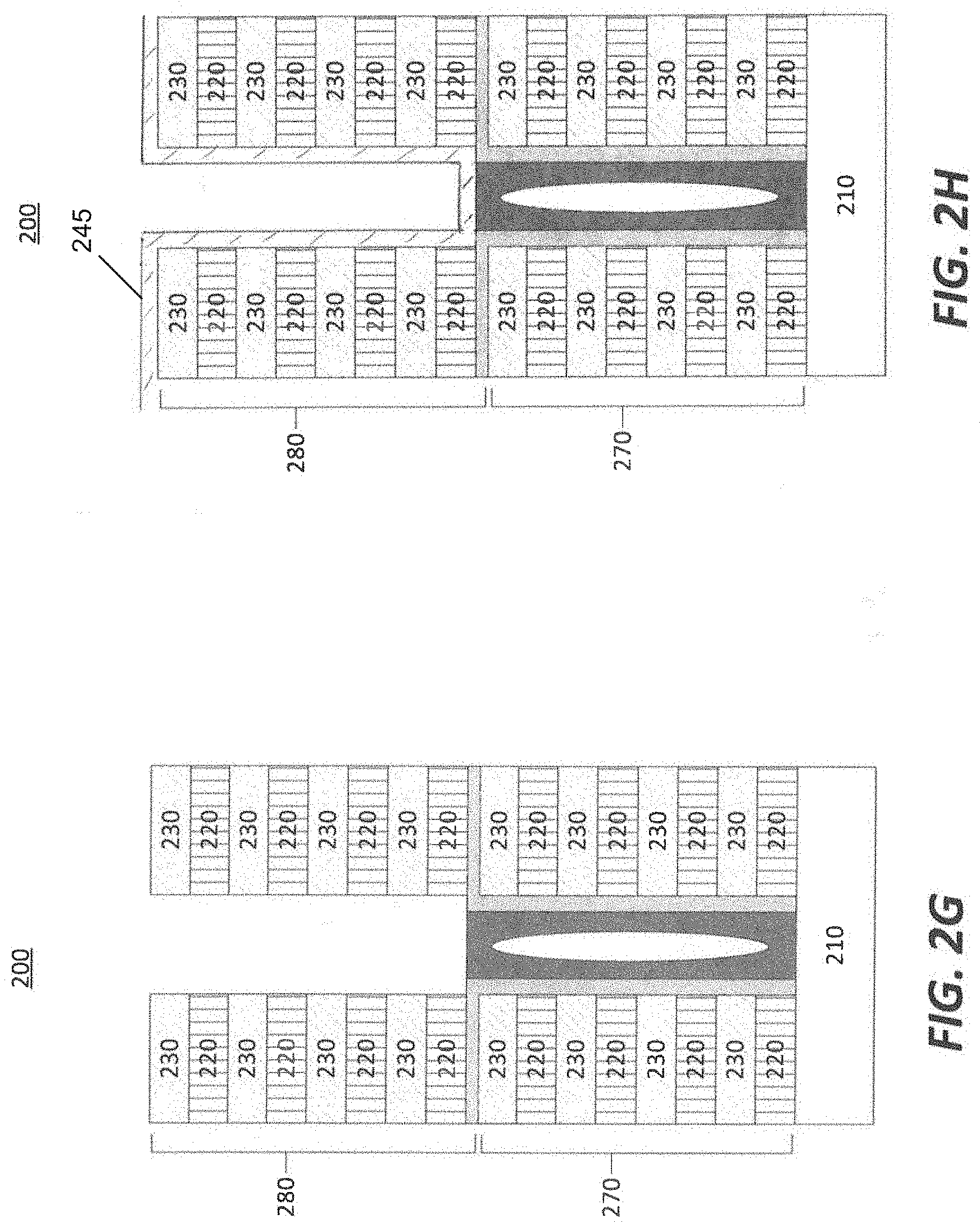
[0035] A second part of the hole may then be formed in the second structure e.g. stack 280 via a dry etch process. The dry etch process may be anisotropic. The etch process may be accomplished with the aid of an etch mask created with lithography, for example. The dry etch process may utilize a halide chemistry with fluorine such as NF.sub.3, CHF.sub.3, SF.sub.6, CF.sub.4, C.sub.2F.sub.2 and their mixtures, for example. The dry etch process may involve a plasma, for example. The dry etch chemistry may involve oxygen or ozone in some cases. The liner 240 and the plug fill 250 may function as an etch stop for the etch process. The liner 240 and the plug fill 250 may remain left over after the etch process as shown in FIG. 2G and FIG. 2H.
[0036] Optionally, a second liner 245 may be added to the second structure e.g. stack 280 as shown in FIG. 2H. The second liner 245 may comprise silicon, an oxide, a nitride and or a carbide layer. The second liner may for example comprise silicon oxy carbide nitride (SiOCN), aluminum nitride and/or boron carbide. Depositing the second liner therefore comprises providing a nitrogen or oxide comprising reactant.
[0037] The second liner 245 may cover the tops and sides of the oxide layer 230 and the nitride layer 220 bilayer stack of the second structure (in the second part of the hole). The second liner 245 may also extend to cover an exposed portion of the plug fill 250 (in the bottom of the second part of the hole). The second liner may be deposited in batch in a reaction chamber of a vertical furnace. The method may therefore comprise loading the substrate to a boat and moving the boat with substrates to a reaction chamber of a batch reactor of a vertical furnace for processing. The second liner 245 may be deposited via an Atomic Layer Deposition (ALD) process, a Chemical Vapor Deposition (CVD) process, or an epitaxial process, for example. The second liner may have a thickness smaller than 10, preferably 5 nanometer.
[0038] The second liner 245 may be covering a portion of the plug fill 250 in the bottom of the second part of the hole. The part of the second liner 245 in the bottom of the second part of the hole may be removed with an anisotropic dry etch. For example with a reactive ion etch (ME).
[0039] The plug fill 250 may then be removed with a dry etch. The dry etch may be isotropic. The etching may be accomplished in a reaction chamber of a batch reactor of a vertical furnace or in a reaction chamber of a single wafer reactor.
[0040] When a furnace is used, the substrate 210 may be loaded to a boat having space to accommodate 25 to 250 substrates. The boat with substrates may be moved into the reaction chamber of the reactor.
[0041] The batch or single wafer reactor may be constructed and arranged to provide a gaseous etchant to the reaction chamber for isotropic etching the plug fill 250. For example, the reactor may be constructed to provide one or more gaseous etchants comprising a halide to the reaction chamber. The halides may be selected from chlorides and fluorides. The halides may be selected from nitrogen trifluoride NF.sub.3, chlorine Cl.sub.2, hydrogen chloride (HCl); hydrogen fluoride (HF); hydrogen bromide (HBr); boron chloride (BCl.sub.3); fluorine (F.sub.2) for dry etching the plug fill 250.
[0042] The dry etch may be thermally activated. The temperature in the reactor may be kept below 500.degree. C. to not harm temperature sensitive structures in the intermediate product. The pressure in the reactor may be kept below 1 Torr. The reaction chamber may be kept substantially radical and/or ion free. A suitable etchant at these temperatures may be chlorine Cl.sub.2.
[0043] A dry etch with gaseous chlorine Cl.sub.2 will not suffer from capillary effects in the hole as with a wet etch. A good etching of the plug fill may therefore be achieved with a dry etch with gaseous chlorine Cl.sub.2. The dry etch may not leave a residue. Damage to either the nitride layer 220 and/or the oxide layer 230 by the dry etch used for the removal may be circumvented. Using the thermally activated dry etch may be scalable so that when the holes may become deeper and narrower with the next technology nodes dry etch may still give the best etching. The reactivity and therefor the etch speed but also the damage potential of the thermally activated dry etch may be carefully tuned by varying the temperature in the reaction chamber.
[0044] The main time limiting factor for the dry etch may also be caused by the depth and width of the holes created. The diffusion speed of the reactant and reaction by-products are determined by the depth and width of the holes created. This limiting factor may be substantially the same for a substrate processed in a batch reactor as for a single wafer (substrate) reactor and may become longer with future technology nodes where the holes may become narrower and deeper. Since only one substrate may be processed every time in a single wafer tool the throughout penalty caused by diffusion speed may be much larger in a single wafer tool compared to a batch reactor where 25 to 175 substrates may be processed simultaneously. A batch reactor may therefore be preferred for dry etching the narrow holes.
[0045] The dry etch may substantially strip away the plug fill 250 comprising germanium at a faster rate than removing silicon. For example, a thermally activated dry etch with Cl.sub.2 of SiGe (50%) in the plug fill 250 may result in an etch rate that is more than 1000 times higher than the etch rate of SiO/SiN used in the bilayers of the structures. Dry etch with Cl.sub.2 of SiGe (50%) in the plug fill 250 may result in an etch rate that is more than 200 times higher than the etch rate of Si used in the first or second liners 240, 245.
[0046] The dry etch of SiGe with Cl.sub.2 may be done at a temperature between 250 and 450.degree. C. and preferably between 300 and 400.degree. C. At 350.degree. C., for example an high etch rate between 10 to 200 or 75-100 nm/minute may be achievable for the SiGe plug fil 250. The etch rate of the first and second silicon liner may be 0.1 to 2 or around 0.4 nm/min. under the same circumstances. The first and second liners 240, 245 of Si may therefore protect the first and second structures while the SiGe plug fill 250 is removed. The Si liners remain conformal over the first and second structures after the etch of the SiGe plug fill 250 minimizing the risk on attacking the underlying first and second structures.
[0047] Etch rates of the plug fill 250 may range between 1 and 1000 nm/min., between 10 and 100 nm/min., or between 1 and 10 nm/min. The first and second liner 240, 245 may protect the bilayers of the first and second structure during the dry etch.
[0048] After the plug fill 250 is removed and the optional first and second liners are used, the first and second liners 240, 245 may still remain (see FIG. 2I). The first and second liners 240, 245 may then be removed via an additional dry etch. The etching may also be accomplished with for example a batch reactor of a vertical furnace or a single wafer reactor. When a furnace is used, the substrate 210 may be provided to a boat having space to accommodate 25 to 250 substrates. The boat with substrates may be moved into a reaction chamber of the reactor. This may be the same reactor as used for etching the plug fill 250.
[0049] The batch or single wafer reactor may be constructed and arranged to provide a gaseous etchant to the reaction chamber for isotropic etching the first and second liners 240, 245. For example, the reactor may be constructed to provide one or more gaseous etchants comprising a halide to the reaction chamber. The halide may be selected from nitrogen trifluoride NF.sub.3, chlorine Cl.sub.2, hydrogen chloride (HCl); hydrogen fluoride (HF); hydrogen bromide (HBr); boron chloride (BCl.sub.3); fluorine (F.sub.2) for dry etching the first liner 240.
[0050] The temperature in the reactor may be kept below 500.degree. C., between 350 and 500.degree. C. and preferably between 375 and 450.degree. C. and the pressure in the reactor may be kept below 1 Torr. The reaction chamber may be kept substantially radical and/or ion free. The removal of the plug fill 250 and the first and second liners may be done in situ in the same reactor or in the same tool to avoid oxidization when the product is transported in a not controlled atmosphere (e.g. with oxygen or water in it).
[0051] The dry etch of the first or second liner may be done with Cl.sub.2 at a temperature between 350 and 500.degree. C. and preferably between 375 and 450.degree. C. For example dry etch with Cl.sub.2 of Si in the first and second liner 240, 245 may result in an etch rate that is more than 10 times higher than the etch rate of SiO/SiN used in the bilayers of the structures. The etch rate of the first and second liner if Si is used may be between 0.1 to 10 or around 1 nm/min at 410.degree. C. with Cl.sub.2. So the plug fill 250 may be dry etched at 350.degree. C. until it is completely removed and subsequently the first and second liner 240, 245 may be dry etched by increasing the temperature to 410 or 420.degree. C. The plug fill 250 and the first and second liner 240, 245 may therefore be dry etched in the same reaction chamber which improves the efficiency and cleanness of the etch process.
[0052] What remains is a structure combining the first and second structure with the hole formed by the first and second hole part and forming the intermediate product 200 as shown in FIG. 2J. At this point, manufacture of the intermediate product 200 may be complete, or steps may be repeated in order to form additional structures e.g. stacks on top of the intermediate product 200.
[0053] FIG. 3 illustrates a method 300 for manufacturing a 3-D NAND device in accordance with at least one embodiment of the invention. The method 300 starts after a first structure has been deposited on a substrate to create an intermediate product. The intermediate product then is processed by: a dry etch step 310 with for example a plasma to create a first part of the hole with an anisotropic etch; a first liner deposition step 320; a plug fill step 330; a polishing step 340; a second structure deposition step 350; a second dry etch step 360 with for example a plasma to create a second part of the hole with an anisotropic etch; optionally and not depicted a second liner deposition step; a plug fill dry etch step 370 (strip) with a gaseous etchant for an isotropic etch, and optionally and not depicted a first and second liner dry etch step with also a gaseous etchant for an isotropic etch. The first and second liner dry etch step may not be needed if the plug fill dry etch 370 also removes the first and/or second liners or if no first or second liner is used. Steps 310-370 can be repeated, as illustrated by loop 380.
[0054] The methods of forming the 3-D NAND device may take place in an ALD reaction chamber, a chemical vapor deposition (CVD) chamber, an epitaxial reaction chamber, an etch reactor, a batch reaction chamber, a mini-batch reaction chamber, or a single wafer reaction chamber, for example. The proper reaction chamber may allow for all or a large part of these processes to occur as an in-situ process.
[0055] FIG. 4 illustrates a 3-D NAND device 400 made in accordance with at least one embodiment of the invention. The 3-D NAND device 400 comprises a substrate 410, an oxide-nitride layer stack section 420, a source line 430, and a bit-line electrode section 440. The oxide-nitride layer stack section 420 may also comprise a plurality of channel holes.
[0056] The particular implementations shown and described are illustrative of the invention and its best mode and are not intended to otherwise limit the scope of the aspects and implementations in any way. Indeed, for the sake of brevity, conventional manufacturing, connection, preparation, and other functional aspects of the system may not be described in detail. Furthermore, the connecting lines shown in the various figures are intended to represent exemplary functional relationships and/or physical couplings between the various elements. Many alternative or additional functional relationship or physical connections may be present in the practical system, and/or may be absent in some embodiments.
[0057] It is to be understood that the configurations and/or approaches described herein are exemplary in nature, and that these specific embodiments or examples are not to be considered in a limiting sense, because numerous variations are possible. The specific routines or methods described herein may represent one or more of any number of processing strategies. Thus, the various acts illustrated may be performed in the sequence illustrated, in other sequences, or omitted in some cases.
[0058] The subject matter of the present disclosure includes all novel and nonobvious combinations and subcombinations of the various processes, systems, and configurations, and other features, functions, acts, and/or properties disclosed herein, as well as any and all equivalents thereof.
* * * * *
D00000
D00001
D00002
D00003
D00004
D00005
D00006
D00007
D00008
D00009
D00010
XML
uspto.report is an independent third-party trademark research tool that is not affiliated, endorsed, or sponsored by the United States Patent and Trademark Office (USPTO) or any other governmental organization. The information provided by uspto.report is based on publicly available data at the time of writing and is intended for informational purposes only.
While we strive to provide accurate and up-to-date information, we do not guarantee the accuracy, completeness, reliability, or suitability of the information displayed on this site. The use of this site is at your own risk. Any reliance you place on such information is therefore strictly at your own risk.
All official trademark data, including owner information, should be verified by visiting the official USPTO website at www.uspto.gov. This site is not intended to replace professional legal advice and should not be used as a substitute for consulting with a legal professional who is knowledgeable about trademark law.