Methods For Forming A Polycrystalline Molybdenum Film Over A Surface Of A Substrate And Related Structures Including A Polycrystalline Molybdenum Film
Zope; Bhushan ; et al.
U.S. patent application number 16/994025 was filed with the patent office on 2021-02-25 for methods for forming a polycrystalline molybdenum film over a surface of a substrate and related structures including a polycrystalline molybdenum film. The applicant listed for this patent is ASM IP Holding B.V.. Invention is credited to Roghayyeh Lotfi, Mustafa Muhammad, Eric Shero, Eric Christopher Stevens, Shankar Swaminathan, Bhushan Zope.
| Application Number | 20210054500 16/994025 |
| Document ID | / |
| Family ID | 1000005077328 |
| Filed Date | 2021-02-25 |


View All Diagrams
| United States Patent Application | 20210054500 |
| Kind Code | A1 |
| Zope; Bhushan ; et al. | February 25, 2021 |
METHODS FOR FORMING A POLYCRYSTALLINE MOLYBDENUM FILM OVER A SURFACE OF A SUBSTRATE AND RELATED STRUCTURES INCLUDING A POLYCRYSTALLINE MOLYBDENUM FILM
Abstract
Methods for forming a polycrystalline molybdenum film over a surface of a substrate are disclosed. The methods may include: providing a substrate into a reaction chamber; depositing a nucleation film directly on an exposed surface of the substrate, wherein the nucleation film comprises one of a metal oxide nucleation film or a metal nitride nucleation film; and depositing a polycrystalline molybdenum film directly on the nucleation film; wherein the polycrystalline molybdenum film comprises a plurality of molybdenum crystallites having an average crystallite size of less than 80 .ANG.. Structures including a polycrystalline molybdenum film disposed over a surface of a substrate with an intermediate nucleation film are also disclosed.
| Inventors: | Zope; Bhushan; (Phoenix, AZ) ; Stevens; Eric Christopher; (Tempe, AZ) ; Swaminathan; Shankar; (Phoenix, AZ) ; Lotfi; Roghayyeh; (Scottsdale, AZ) ; Muhammad; Mustafa; (Gilbert, AZ) ; Shero; Eric; (Phoenix, AZ) | ||||||||||
| Applicant: |
|
||||||||||
|---|---|---|---|---|---|---|---|---|---|---|---|
| Family ID: | 1000005077328 | ||||||||||
| Appl. No.: | 16/994025 | ||||||||||
| Filed: | August 14, 2020 |
Related U.S. Patent Documents
| Application Number | Filing Date | Patent Number | ||
|---|---|---|---|---|
| 62891247 | Aug 23, 2019 | |||
| 62891254 | Aug 23, 2019 | |||
| Current U.S. Class: | 1/1 |
| Current CPC Class: | C23C 16/0272 20130101; H01L 27/10891 20130101; C23C 16/45553 20130101; C23C 16/08 20130101; C23C 16/45527 20130101; C23C 16/34 20130101; G11C 5/063 20130101; H01L 27/10823 20130101; H01L 27/10876 20130101 |
| International Class: | C23C 16/34 20060101 C23C016/34; C23C 16/02 20060101 C23C016/02; C23C 16/08 20060101 C23C016/08; C23C 16/455 20060101 C23C016/455; G11C 5/06 20060101 G11C005/06; H01L 27/108 20060101 H01L027/108 |
Claims
1. A method for forming a polycrystalline molybdenum film over a surface of a substrate, the method comprising: providing a substrate into a reaction chamber; depositing a nucleation film directly on an exposed surface of the substrate, wherein the nucleation film comprises one of a metal oxide nucleation film or a metal nitride nucleation film; and depositing a polycrystalline molybdenum film directly on the nucleation film; wherein the polycrystalline molybdenum film comprises a plurality of molybdenum crystallites having an average crystallite size of less than 80 Angstroms.
2. The method of claim 1, wherein depositing the nucleation film comprises performing one or more first unit deposition cycles of a first cyclical deposition process, wherein a first unit deposition cycle comprises, sequentially contacting the substrate with a metal precursor and with one of an oxygen precursor, or a nitrogen precursor.
3. The method of claim 1, wherein depositing the polycrystalline molybdenum metal film comprises performing one or more second unit deposition cycles of a second cyclical deposition process, wherein a second unit deposition cycle comprises, sequentially contacting the substrate with a molybdenum halide precursor and a reducing agent.
4. The method of claim 3, wherein the molybdenum halide precursor comprises at least one of: molybdenum (V) trichloride oxide (MoOCl.sub.3), molybdenum (VI) tetrachloride oxide (MoOCl.sub.4), or molybdenum (IV) dichloride dioxide (MoO.sub.2Cl.sub.2).
5. The method of claim 1, wherein the metal oxide nucleation film comprises at least one of: an aluminum oxide nucleation film, a molybdenum oxide nucleation film, a tungsten oxide nucleation film, a ruthenium oxide nucleation film, a rhenium oxide nucleation film, or an iridium oxide nucleation film, and the metal oxide nucleation film has an average film thickness of less than 50 .ANG..
6. The method of claim 1, wherein the metal nitride nucleation film comprises a molybdenum nitride nucleation film, and the molybdenum nitride nucleation film has an average film thickness of less than 30 .ANG..
7. The method of claim 1, wherein the polycrystalline molybdenum film is deposited within a plurality of non-planar features, wherein the polycrystalline molybdenum film fills the plurality of non-planar features without the formation of a seam.
8. The method of claim 1, wherein a bilayer comprising the polycrystalline molybdenum film and the nucleation film has an electrical resistivity of less 25 .mu..OMEGA.-cm for an average nucleation film thickness of less than 20 .ANG., and an average polycrystalline molybdenum film thickness of less than 100 .ANG..
9. The method of claim 1, wherein the nucleation film is a physically continuous film at an average film thickness of less than 50 .ANG..
10. The method of claim 1, wherein the exposed surface of the substrate includes a plurality of vertical non-planar features and the nucleation film is deposited directly on the exposed surface, and the polycrystalline molybdenum film is deposited directly on the nucleation film, wherein the polycrystalline molybdenum film fills the plurality of vertical non-planar features without the formation of a seam.
11. The method of claim 10, wherein the exposed surface comprises a dielectric surface.
12. The method of claim 10, wherein the substrate further comprises a plurality of line features, wherein the percentage line bending of the plurality of line features is less than 20% post deposition of the nucleation film and the polycrystalline molybdenum film.
13. The method of claim 10, wherein the substrate further comprises a plurality of line features, wherein the percentage line bending of the plurality of line features is less than 10% post deposition of the nucleation film and the polycrystalline molybdenum film.
14. The method of claim 10, wherein the nucleation film comprises a molybdenum nitride nucleation film.
15. The method of claim 14, wherein the polycrystalline molybdenum film has an average crystallite size of less than 60 .ANG..
16. The method of claim 1, wherein the polycrystalline molybdenum film has a percentage roughness of less than 10%.
17. The method of claim 1, wherein the polycrystalline molybdenum film has a percentage roughness of less than 5%.
18. The method of claim 1, wherein the nucleation film comprises a molybdenum nitride nucleation film and the polycrystalline molybdenum film has a percentage roughness of less than 10%.
19. The method of claim 1, wherein the exposed surface of the substrate comprising a dielectric surface.
20. A structure comprising the polycrystalline molybdenum film formed according to the method of claim 1.
21. A reaction system configured to perform the method of claim 1.
22. A structure comprising: a surface of a substrate; a nucleation film disposed directly on the surface of the substrate, wherein the nucleation film comprises at least one of a metal oxide nucleation film or a metal nitride nucleation film; and a polycrystalline molybdenum film disposed directly on the nucleation film; wherein the polycrystalline molybdenum film comprises a plurality of molybdenum crystallites having an average crystallite size of less than 80 .ANG..
23. The structure of claim 22, where the metal oxide nucleation film comprises at least one of: an aluminum oxide nucleation film, a molybdenum oxide nucleation film, a tungsten oxide nucleation film, a ruthenium oxide nucleation film, a rhenium oxide nucleation film, or an iridium oxide nucleation film, and the metal oxide nucleation film has an average film thickness of less than 50 .ANG..
24. The structure of claim 22, wherein the metal nitride nucleation film comprises a molybdenum nitride nucleation film having an average film thickness of less than 30 .ANG..
25. The structure of claim 22, wherein the polycrystalline molybdenum film is disposed within a plurality of non-planar features, wherein the polycrystalline molybdenum film fills the plurality of non-planar features without an observable seam.
26. The structure of claim 22, wherein a bilayer comprising the polycrystalline molybdenum film and the nucleation film has an electrical resistivity of less than 25 .mu..OMEGA.-cm for an average nucleation film thickness of less than 20 .ANG. and an average polycrystalline molybdenum film thickness of less than 100 .ANG..
27. The structure of claim 22, wherein the nucleation film is a physically continuous film with an average film thickness of less than 40 .ANG..
28. The structure of claim 22, wherein the surface of the substrate further comprises a plurality of vertical non-planar features and the nucleation film is disposed directly on the plurality of vertical non-planar features and the polycrystalline molybdenum film is disposed directly on the nucleation film, wherein the polycrystalline molybdenum film fills the plurality of vertical non-planar features without an observable seam.
29. The structure of claim 22, wherein the surface of the substrate comprises a dielectric surface.
30. The structure of claim 28, wherein the substrate further comprises a plurality of line features, wherein the percentage line bending of the plurality of line features is less than 20%.
31. The structure of claim 28, wherein the substrate further comprises a plurality of line features, wherein the percentage line bending of the plurality of line features is less than 10%.
32. The structure of claim 28, wherein the nucleation film comprises a molybdenum nitride nucleation film.
33. The structure of claim 32, wherein the polycrystalline molybdenum film has an average crystallite size of less than 60 .ANG..
34. The structure of claim 22, wherein the polycrystalline molybdenum film has a percentage roughness of less than 10%.
35. The structure of claim 22, wherein the substrate comprises a partially fabricated device structure including at least one of: a DRAM device structure, a 3D-NAND device structure, a 3D-integrated device structure, or an integrated logic device structure.
36. The structure of claim 35, wherein the substrate comprises a partially fabricated DRAM device structure, wherein the substrate comprises a plurality of DRAM buried wordline trenches and a plurality of DRAM wordlines.
37. The structure of claim 36, wherein the nucleation film is disposed directly on the plurality of DRAM buried wordline trenches and directly on the plurality of DRAM wordlines.
38. The structure of claim 37, wherein the polycrystalline molybdenum film is disposed within and fills the plurality of DRAM buried word line trenches.
39. The structure of claim 38, wherein the percentage line bending of the plurality of DRAM wordlines is less than 20%.
40. The structure of claim 39, wherein the nucleation film comprises a molybdenum nitride nucleation film and the polycrystalline molybdenum film has a percentage roughness of than 1.5%.
Description
CROSS-REFERENCE TO RELATED APPLICATION
[0001] This Application is a nonprovisional of, and claims priority to and the benefit of, U.S. Provisional Patent Application No. 62/891,247, filed on Aug. 23, 2019 and entitled "METHODS FOR FORMING A POLYCRYSTALLINE MOLYBDENUM FILM OVER A SURFACE OF A SUBSTRATE AND RELATED STRUCTURES INCLUDING A POLYCRYSTALLINE MOLYBDENUM FILM," and U.S. Provisional Patent Application No. 62/891,254, filed on Aug. 23, 2019 and entitled "METHODS FOR DEPOSITING A MOLYBDENUM NITRIDE FILM ON A SURFACE OF A SUBSTRATE BY A CYCLICAL DEPOSITION PROCESS AND RELATED SEMICONDUCTOR DEVICE STRUCTURES INCLUDING A MOLYBDENUM NITRIDE FILM," both of which are hereby incorporated by reference herein.
FIELD OF INVENTION
[0002] The present disclosure relates generally to methods for forming a polycrystalline molybdenum film over a surface of a substrate and particular methods for depositing a nucleation film directly on a surface of a substrate and subsequently depositing a polycrystalline molybdenum film directly on the nucleation film. The present disclosure also general relates to structures including a polycrystalline molybdenum film disposed directly on a nucleation film.
BACKGROUND OF THE DISCLOSURE
[0003] Semiconductor device fabrication processes in advanced technology nodes generally require state of the art deposition processes for forming metal films, such as, polycrystalline molybdenum films, for example.
[0004] A common requisite for the deposition of a metal film is that the deposition process is extremely conformal. For example, conformal deposition is often required in order to uniformly deposit a metal film over three-dimensional structures including high aspect ratio non-planar features. Another common requirement for the deposition of metal films is that the deposition process is capable of depositing ultra-thin films which are continuous over a large substrate area. In the particular case wherein the metal film is electrically conductive, the deposition process may need to be optimized to produce low electrical resistivity films. For example, low electrical resistivity metal films commonly utilized in state of the art semiconductor device applications may include tungsten and/or copper. However, tungsten films and copper films commonly require a thick barrier layer, disposed between the metal film and a dielectric material. The thick barrier layer may be utilized to prevent diffusion of metal species into the underlying dielectric material thereby improving device reliability and device yield. However, the thick barrier layer commonly exhibits a high electrical resistivity and therefore results in an increase in the overall electrical resistivity of the semiconductor device structure.
[0005] Potential replacements for tungsten and copper films in next-generation devices may include molybdenum films. For example, molybdenum (Mo) is a low electrical resistivity refractory metal that can potentially replace tungsten as a material in memory, logic, and other devices using polysilicon-metal gate electrode structures. A molybdenum film can also be used in some organic light emitting diodes, liquid crystal displays, and also in thin film solar cells and photovoltaics.
[0006] In addition, in particular semiconductor fabrication processes, it may be desirable to form a metal film, such as, for example, a polycrystalline molybdenum film, within non-planar features (e.g., vertical and/or horizontal trenches) disposed in/on a substrate. The formation of a metal film within non-planar features may at least partially or fully fill the non-planar features with the metal film, a process commonly referred to as "gap-fill". As semiconductor device structure geometries have decreased and high aspect ratio non-planar features have become more common place in device structures such as DRAM, 3D-NAND, flash memory, and logic, it has become increasingly difficult to fill non-planar features with a metal film having the desired characteristics.
[0007] Accordingly, methods and related structures are desired for forming a polycrystalline molybdenum film with low electrical resistivity and physical properties that enable a polycrystalline molybdenum gap-fill process on a substrate including non-planar features.
SUMMARY OF THE DISCLOSURE
[0008] This summary is provided to introduce a selection of concepts in a simplified form. These concepts are described in further detail in the detailed description of example embodiments of the disclosure below. This summary is not intended to identify key features or essential features of the claimed subject matter, nor is it intended to be used to limit the scope of the claimed subject matter.
[0009] In some embodiments, methods for forming a polycrystalline molybdenum film over a surface of a substrate are provided. The methods may comprise: providing a substrate into a reaction chamber; depositing a nucleation film directly on an exposed surface of the substrate, wherein the nucleation film comprises one of a metal oxide nucleation film or a metal nitride nucleation film; and depositing a polycrystalline molybdenum film directly on the nucleation film, wherein the polycrystalline molybdenum film comprises a plurality of molybdenum crystallites having an average crystallite size of less than 80 .ANG..
[0010] In some embodiments, structures including a polycrystalline molybdenum film are provided. The structures may comprise: a surface of a substrate; a nucleation film disposed directly on the surface of the substrate, wherein the nucleation film comprises at least one of a metal oxide nucleation film or a metal nitride nucleation film; and a polycrystalline molybdenum film disposed directly on the nucleation film; wherein the polycrystalline molybdenum film comprises a plurality of molybdenum crystallites having an average crystallite size of less than 80 .ANG..
[0011] For purposes of summarizing the invention and the advantages achieved over the prior art, certain objects and advantages of the invention have been described herein above. Of course, it is to be understood that not necessarily all such objects or advantages may be achieved in accordance with any particular embodiment of the invention. Thus, for example, those skilled in the art will recognize that the invention may be embodied or carried out in a manner that achieves or optimizes one advantage or group of advantages as taught or suggested herein without necessarily achieving other objects or advantages as may be taught or suggested herein.
[0012] All of these embodiments are intended to be within the scope of the invention herein disclosed. These and other embodiments will become readily apparent to those skilled in the art from the following detailed description of certain embodiments having reference to the attached figures, the invention not being limited to any particular embodiment(s) disclosed.
BRIEF DESCRIPTION OF THE DRAWING FIGURES
[0013] While the specification concludes with claims particularly pointing out and distinctly claiming what are regarded as embodiments of the invention, the advantages of embodiments of the disclosure may be more readily ascertained from the description of certain examples of the embodiments of the disclosure when read in conjunction with the accompanying drawings, in which:
[0014] FIG. 1A illustrates a simplified cross-sectional schematic diagram of a prior art structure which includes a number of vertical trenches;
[0015] FIG. 1B illustrates a simplified cross-sectional schematic diagram of the prior art structure of FIG. 1A following the formation of a gap-fill film within the vertical trenches;
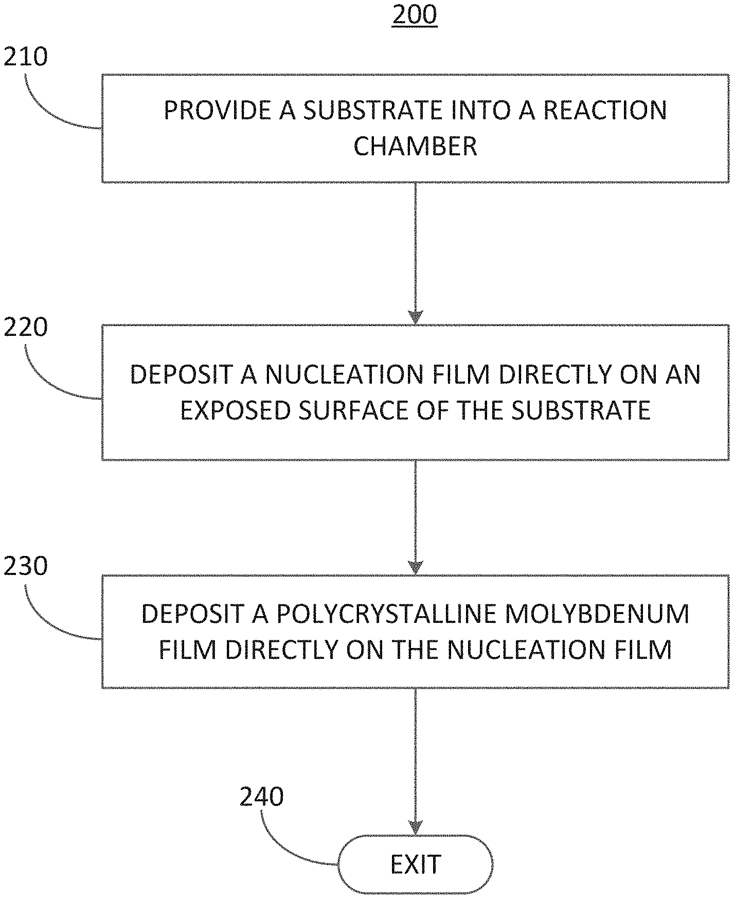
[0016] FIG. 2 illustrates an exemplary process flow, demonstrating a method for forming a polycrystalline molybdenum film over a surface of a substrate according to the embodiments of the disclosure;
[0017] FIG. 3 illustrates an exemplary process flow, demonstrating a first cyclical deposition process for depositing a nucleation film directly on an exposed surface of a substrate according to the embodiments of the disclosure;
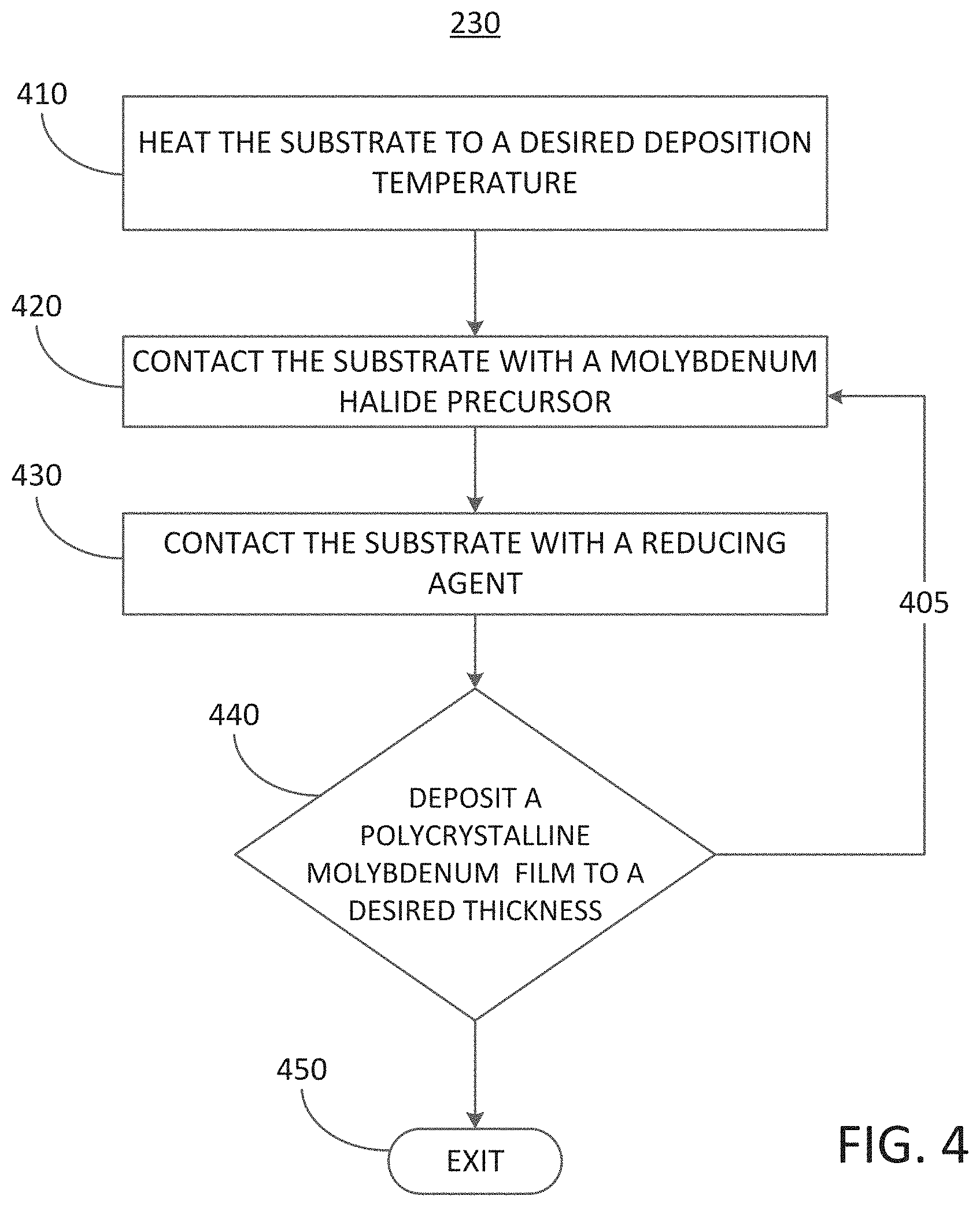
[0018] FIG. 4 illustrates an exemplary process flow, demonstrating a second cyclical deposition process for depositing a polycrystalline molybdenum film directly on a nucleation film according to the embodiments of the disclosure;
[0019] FIG. 5A illustrates a simplified cross-sectional schematic diagram of a structure including a substrate with a number of non-planar features;
[0020] FIG. 5B illustrates a simplified cross-sectional schematic diagram of the structure of FIG. 5A following the deposition of a nucleation film directly on an exposed surface of the substrate according to the embodiments of the disclosure; and
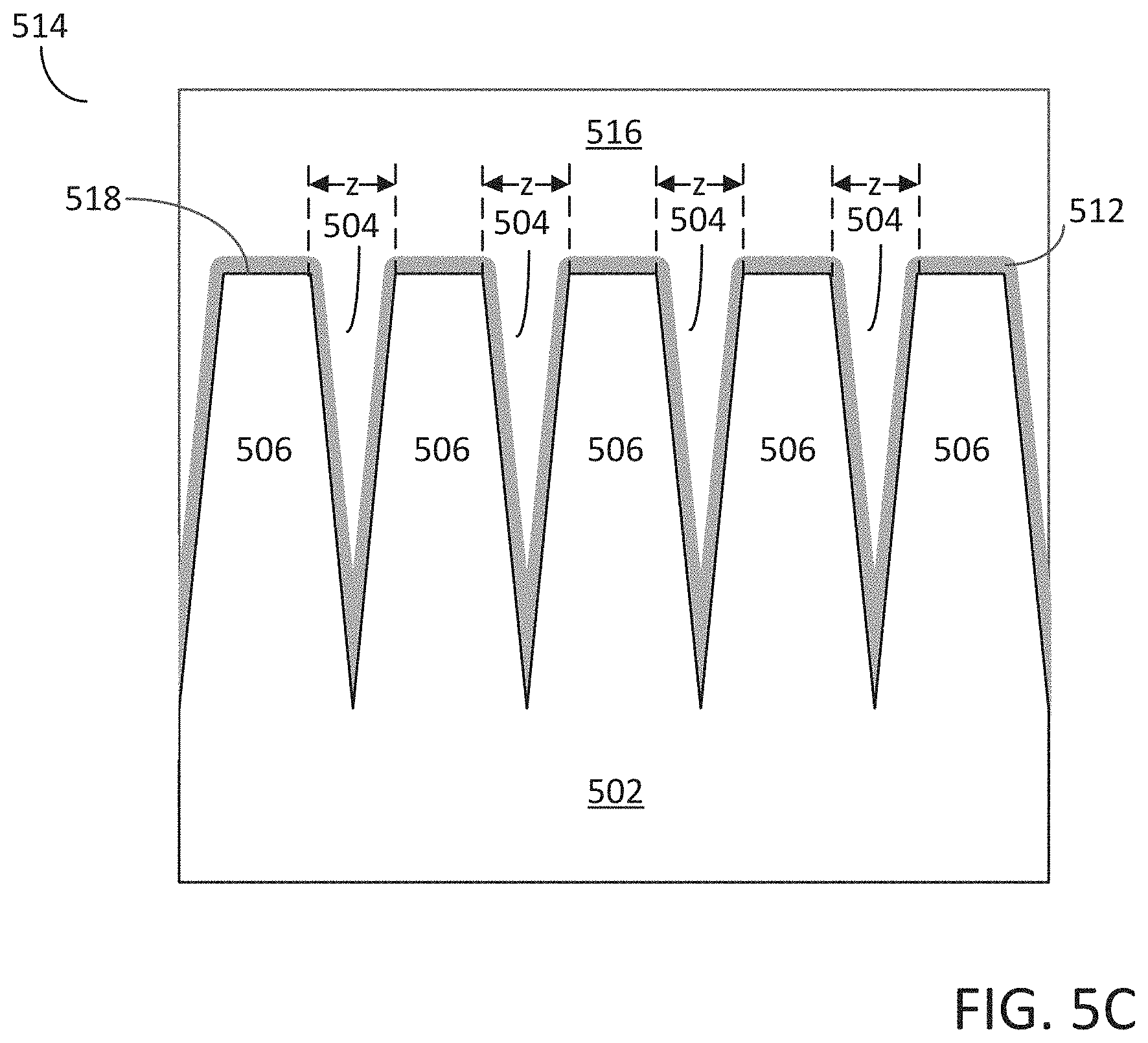
[0021] FIG. 5C illustrates a simplified cross-sectional schematic diagram of the structure of FIG. 5B following the deposition of a polycrystalline molybdenum film directly on the nucleation film according to the embodiments of the disclosure.
DETAILED DESCRIPTION OF EXEMPLARY EMBODIMENTS
[0022] Although certain embodiments and examples are disclosed below, it will be understood by those in the art that the invention extends beyond the specifically disclosed embodiments and/or uses of the invention and obvious modifications and equivalents thereof. Thus, it is intended that the scope of the invention disclosed should not be limited by the particular disclosed embodiments described below.
[0023] The illustrations presented herein are not meant to be actual views of any particular material, structure, or device, but are merely idealized representations that are used to describe embodiments of the disclosure.
[0024] As used herein, the term "substrate" may refer to any underlying material or materials that may be used, or upon which, a structure, a device, a circuit, or a film may be formed.
[0025] As used herein, the term "cyclical deposition" may refer to the sequential introduction of two or more precursors (reactants) into a reaction chamber to deposit a film over a substrate and includes deposition techniques such as atomic layer deposition and cyclical chemical vapor deposition.
[0026] As used herein, the term "cyclical chemical vapor deposition" may refer to any process wherein a substrate is sequentially exposed to two or more volatile precursors, which react and/or decompose on a substrate to deposit a desired film.
[0027] As used herein, the term "atomic layer deposition" (ALD) may refer to a vapor deposition process in which deposition cycles, preferably a plurality of consecutive deposition cycles, are conducted in a reaction chamber. Typically, during each deposition cycle the precursor is chemisorbed to a deposition surface (e.g., a substrate surface or a previously deposited underlying surface such as material from a previous ALD deposition cycle), forming a monolayer or sub-monolayer that does not readily react with additional precursor (i.e., a self-limiting reaction). Thereafter, if necessary, a reactant (e.g., another precursor or reaction gas) may subsequently be introduced into the reaction chamber for use in converting the chemisorbed precursor to the desired material on the deposition surface. Typically, this reactant is capable of further reaction with the precursor. Further, purging steps may also be utilized during each deposition cycle to remove excess precursor from the reaction chamber and/or remove excess reactant and/or reaction byproducts from the reaction chamber after conversion of the chemisorbed precursor. Further, the term "atomic layer deposition," as used herein, is also meant to include processes designated by related terms such as, "chemical vapor atomic layer deposition", "atomic layer epitaxy" (ALE), molecular beam epitaxy (MBE), gas source MBE, or organometallic MBE, and chemical beam epitaxy when performed with alternating pulses of precursor composition(s), reactive gas, and purge (e.g., inert carrier) gas.
[0028] As used herein, the term "film" may refer to any physical continuous or physically discontinuous structures and materials formed or deposited by the methods disclosed herein. For example, "film" could include 2D materials, nanolaminates, nanorods, nanotubes, nanoparticles, partial or full molecular layers, partial or full atomic layers, or clusters of atoms and/or molecules. "Film" may also comprise a material or a layer with pinholes, but still be at least partially continuous.
[0029] As used herein, the term "molybdenum halide precursor" may refer to a reactant which comprises at least a molybdenum component and a halide component, wherein the halide component may include one or more of a chlorine component, an iodine component, or a bromine component.
[0030] As used herein, the term "molybdenum oxyhalide" may refer to a reactant which comprises at least a molybdenum component, an oxygen component, and a halide component.
[0031] As used herein, the term "reducing agent" may refer to a reactant that donates an electron to another species in a redox chemical reaction.
[0032] As used herein, the term "polycrystalline film" may refer to a film which displays at least short range ordering of the crystalline structure of the film and also includes the terms "multicrystalline film", or "polycrystal film". "Polycrystalline film" also may refer to a film comprising a plurality of crystallites.
[0033] As used herein, the terms "amorphous" and "amorphous film" may refer to a film which displays substantially no ordering of the structure of the film
[0034] As used herein, the term "crystallite size" may refer to average size of a plurality of crystallites within a polycrystalline film as determined by x-ray diffraction (XRD) measurements of the polycrystalline film.
[0035] As used herein, the term "non-planar feature" may refer to an opening or cavity disposed between two opposing surfaces of a non-planar substrate and may include "vertical non-planar features" and "horizontal non-planar features".
[0036] As used herein, the term "vertical non-planar feature" may comprise: an opening or cavity disposed between opposing inclined sidewalls of two protrusions extending upwards from a surface of a substrate, or opposing inclined sidewalls of an indentation extending downward into a surface of a substrate. Non-limiting examples of "vertical non-planar features" may include, but is not limited to: v-shaped vertical trenches, tapered vertical trenches, re-entrant vertical trenches, vertical openings, vertical voids, and vertical through-silicon-via trenches. For example, a vertical non-planar feature may comprise adjacent sidewalls which meet at a point at the base of the feature, or a vertical non-planar feature may comprise a base of the feature that plateaus to a flat base surface. "Vertical" as used herein does not limit the slope of opposing sidewalls specifically to a perpendicular incline with the horizontal plane of the substrate.
[0037] As used herein, the term "horizontal non-planar feature" may comprise: an opening or cavity disposed between two opposing substantially horizontal surfaces, the opposing substantially horizontal surfaces bounding the "horizontal non-planar feature".
[0038] As used herein, the term "line bending" may refer to a bending or a distortion of the regions of the substrate disposed between adjacent non-planar features, the bending or distortion resulting from the formation of a gap-fill film within the non-planar features. For example, a non-planar substrate may comprise a plurality of "vertical non-planar features" such as, vertical trenches, extending downward into the substrate. The regions between adjacent "vertical non-planar features" may be referred as line features. The line features may undergo a line bending (i.e., a distortion) upon the formation of a gap-fill metal within a substrate including a plurality of non-planar features.
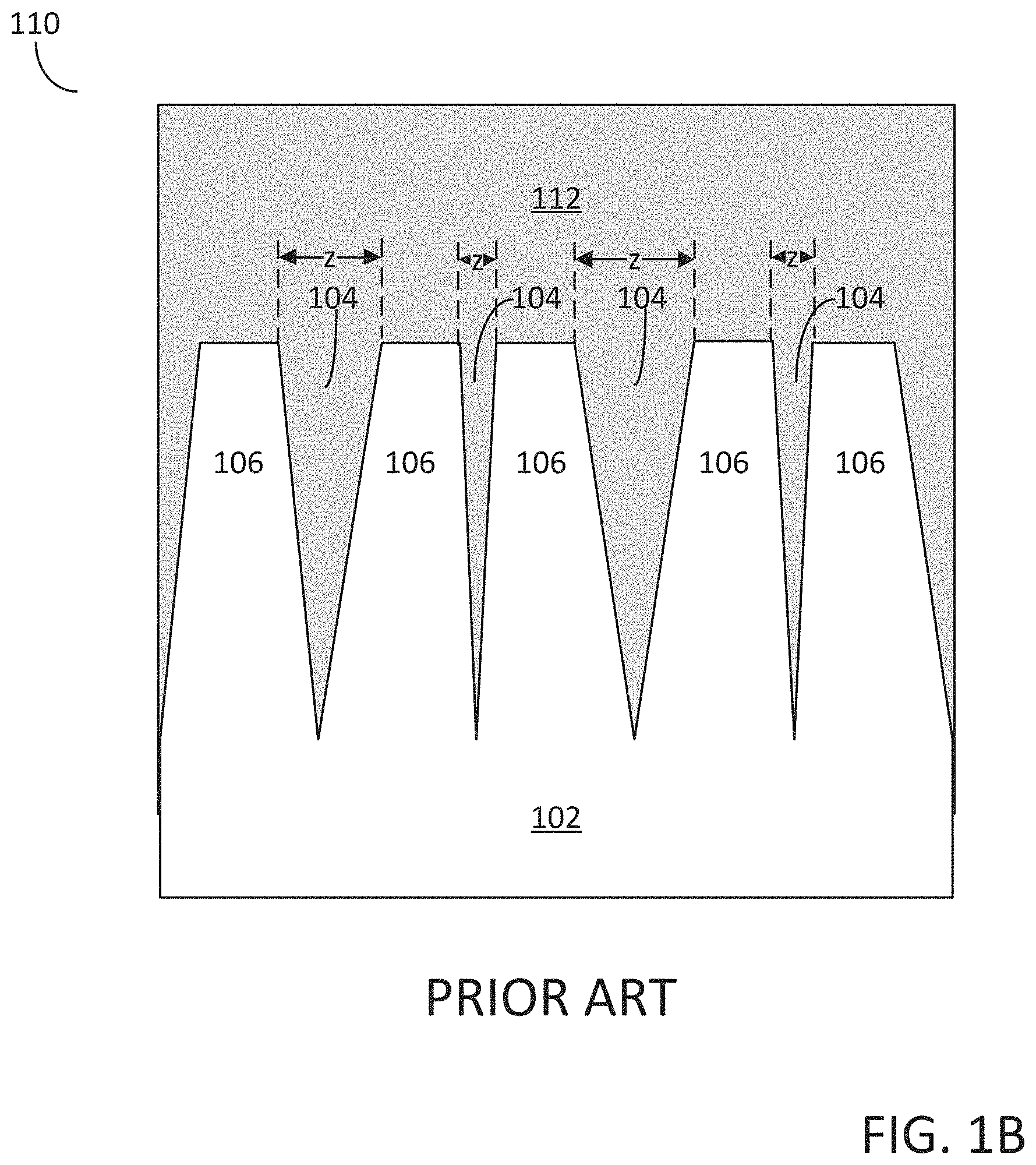
[0039] The concept of "line bending" is illustrated in greater detail with reference to FIGS. 1A-B which illustrate prior art methods for forming a gap-fill film within a plurality of non-planar features.
[0040] In more detail, FIG. 1A illustrates a simplified cross-sectional schematic diagram of a structure 100 prior to a gap-fill process. The structure 100 includes a substrate 102 including an array of non-planar features 104, which in this example comprise vertical trenches disposed within the substrate 102. Disposed between each of the adjacent vertical trenches 104 is a plurality of line feature 106. The plurality of line features 106 may have a substantially regular pitch (x), wherein the pitch (x) may be defined as the distance between the middle vertical axis of one line feature (e.g., axis 108A) to the middle vertical axis of an adjacent line feature (e.g., axis 108B). The array of vertical trenches 104 as illustrated in FIG. 1A may comprise sloped sidewalls, wherein the width of each vertical trench decreases from the top/opening of a vertical trench down to the base of the vertical trench. The width (y) of each of the array of vertical trenches may be determined by measurement of the distance between opposing sidewalls of the vertical trench. For example, in the structure 100 of FIG. 1A the vertical trenches comprise v-shaped vertical trenches wherein the width (y) of each the v-shaped trenches may be determined by measuring the distance between the uppermost extent of opposing sidewalls, as illustrated in FIG. 1A.
[0041] As a non-limiting example, the structure 100 of FIG. 1A may comprise a portion of a partially fabricated dynamic random-access memory (DRAM) device structure prior to the deposition of a gap-fill film, wherein the partially fabricated DRAM device structures includes a regular array of buried wordline (bWL) trenches (e.g., vertical trenches 104), and DRAM wordlines (e.g., line features 106).
[0042] FIG. 1B illustrates a simplified cross-sectional schematic diagram of a prior art structure 110 which comprises the structure 100 (of FIG. 1A) following the deposition of a gap-fill film within the array of vertical trenches, thereby filling the vertical trenches with the gap-fill film. As illustrated in FIG. 1B, the line features 106 disposed between adjacent vertical trenches 104 are bent (or distorted) due to the deposition of the gap-fill film 112 and the once regular array of line features 106 are more disordered due to the gap-fill film deposition. The bending of the line features 106 results in an increased variation of the width of the vertical non-planar structures 104 as denoted by width (z), e.g., as measured at the uppermost extent of the v-shaped vertical trenches of FIG. 1B.
[0043] As used herein, the term "percentage line bending" may quantify the degree of line bending caused by the deposition of a gap-fill film on a substrate including a regular array of non-planar features and line features. The percentage line bending may be calculated by the following equation (I):
percentage ( % ) line bending = ( offset pitch ) .times. 100 ( I ) ##EQU00001##
[0044] wherein the offset is calculated by the following equation (II):
offset=|z-y| (II)
[0045] or in other words, the value of the offset equals the absolute value of the average width of the non-planar features (e.g., vertical trenches) pre gap-fill film deposition (average value of (z)), minus the average width of the non-planar features (e.g., vertical trenches) pre gap-fill film deposition (average value (y)). As a non-limiting example, the offset may be statistically established by measuring the width (y) of a plurality of non-planar features prior to gap-fill film deposition and subsequently measuring the width (z) for a plurality of non-planar features following the deposition of a gap-fill film in the non-planar features. The average of (z) and the average of (y) may be determine utilizing high magnification microscopy techniques, such as, scanning electron microscope, for example.
[0046] As used herein, the term "seam" may refer to a line or one or more macro voids formed by the abutment of the leading edges of the gap-fill film. For example, a seam may refer to a region in a metal gap-fill film wherein the leading edges of two metal films growing on opposing sidewalls of a non-planar feature touch each other. Therefore the "seam" is generally disposed at the center of a metal filled non-planar feature. The formation of a seam in a metal gap-fill film may be undesirable and may result in poor device performance and subsequent issues in device fabrication. The presence of a "seam" within a gap-fill film may be observable using scanning transmission electron microscopy (STEM), or transmission electron microscopy (TEM).
[0047] A number of example materials are given throughout the embodiments of the current disclosure, it should be noted that the chemical formulas given for each of the example materials should not be construed as limiting and that the exemplary materials given should not be limited by a given example stoichiometry.
[0048] The present disclosure includes methods for forming a polycrystalline molybdenum film over a surface of a substrate utilizing an intermediate nucleation. Polycrystalline molybdenum films may be utilized in a number of applications, such as, for example, low electrical resistivity metal gap-fill films, liner layers for 3D-NAND, DRAM word-line features, or as an interconnect material in CMOS logic applications. The ability to deposit a polycrystalline molybdenum film over a surface of a substrate utilizing an intermediate nucleation film, i.e., without the use of a high electrical resistivity liner layer, may allow for a lower electrical resistivity for interconnects in logic applications, i.e., CMOS structures, and word-line/bit-line in memory applications, such as 3D-NAND and DRAM structures.
[0049] In addition, the embodiments of the disclosure may provide nucleation films utilized for the deposition of polycrystalline molybdenum films, wherein the nucleation films may improve the quality of the polycrystalline molybdenum films. For example, the deposition of the nucleation films prior to the deposition of the polycrystalline molybdenum film may result in a polycrystalline molybdenum film with a reduced surface roughness and/or a reduced crystallite size. The improved characteristics of the polycrystalline molybdenum films formed according to the embodiments of the disclosure may result in improved a metal gap-fill film and a reduction in the percentage line bending in structures including an array of non-planar features and line features.
[0050] Therefore, the embodiments of the disclosure may include methods for forming a polycrystalline molybdenum film over a surface of a substrate utilizing an intermediate nucleation film. The methods of the disclosure may comprise: providing a substrate into a reaction chamber; depositing a nucleation film directly on an exposed surface of the substrate, wherein the nucleation film comprises one of a metal oxide nucleation film or a metal nitride nucleation film; and depositing a polycrystalline molybdenum film directly on the nucleation film, wherein the polycrystalline molybdenum film comprises a plurality of molybdenum crystallites having an average crystallite size of less than 80 .ANG..
[0051] An exemplary process for forming a polycrystalline molybdenum film over a surface of a substrate utilizing an intermediate nucleation film is illustrated with reference to FIG. 2. The exemplary process 200 (FIG. 2) may comprise two distinct deposition processes, a first deposition process for depositing a nucleation film directly on an exposed surface of a substrate, and a second deposition process for depositing a polycrystalline molybdenum film directly on the nucleation film.
[0052] In more detail and with reference to FIG. 2, the exemplary process 200 may commence by means of a process block 210 which comprises, providing a substrate into a reaction chamber.
[0053] In some embodiments of the disclosure, the substrate may comprise a non-planar substrate including a plurality of non-planar features, as previous described herein. It should be noted that the embodiments of the disclosure are not limited to metal gap-fill methods for filling vertical non-planar features and horizontal non-planar features and that other geometries of non-planar features disposed in and/or on a substrate may be filled with a polycrystalline molybdenum film by the processes disclosed herein.
[0054] In some embodiments, a non-planar substrate may comprise one or more materials and material surfaces including, but not limited to, semiconductors, dielectrics, and metallics.
[0055] In some embodiments, the substrate may include semiconductor materials and surfaces, such as, but not limited to, silicon (Si), germanium (Ge), germanium tin (GeSn), silicon germanium (SiGe), silicon germanium tin (SiGeSn), silicon carbide (SiC), or a group III-V semiconductor materials.
[0056] In some embodiments, the substrate may include metallic materials and surfaces, such as, but not limited to, pure metals, metal nitrides, metal carbides, metal borides, and mixtures thereof.
[0057] In some embodiments, the substrate may include dielectric materials and surfaces, such as, but not limited, to silicon containing dielectric materials and metal oxide dielectric materials. In some embodiments, the silicon containing dielectric materials may comprise one or more of: silicon dioxide (SiO.sub.2), silicon sub-oxides, silicon nitride (Si.sub.3N.sub.4), silicon oxynitride (SiON), silicon oxycarbide (SiOC), silicon oxycarbide nitride (SiOCN), silicon carbon nitride (SiCN). In some embodiments, the metal oxide dielectric materials may comprise one or more of: aluminum oxide (Al.sub.2O.sub.3), hafnium oxide (HfO.sub.2), tantalum oxide (Ta.sub.2O.sub.5), zirconium oxide (ZrO.sub.2), titanium oxide (TiO.sub.2), hafnium silicate (HfSiO.sub.x), and lanthanum oxide (La.sub.2O.sub.3).
[0058] In some embodiments of the disclosure, the substrate may comprise an engineered substrate wherein a semiconductor layer is disposed over a bulk support with an intervening buried oxide (BOX) disposed there between.
[0059] In some embodiments, the substrates utilized in the processes described herein may include device structures, including partially fabricated device structures, formed into or onto a surface of the substrate. For example, a substrate may comprise fabricated and/or partially fabricated device structures, such as, for example, transistors and/or memory elements. In some embodiments, the substrate may contain monocrystalline surfaces and/or one or more secondary surfaces that may comprise a non-monocrystalline surface, such as a polycrystalline surface and/or an amorphous surface.
[0060] The substrate may be loaded into a reaction chamber configured for forming a polycrystalline molybdenum film. In some embodiments, the nucleation film may be deposited directly on an exposed surface of the substrate by one or more deposition processes, including, but not limited to, a chemical vapor deposition (CVD) process, a soak deposition process, a plasma-enhanced chemical vapor deposition (PECVD) process, or a physical vapor deposition (PVD) process. In particular embodiments of the disclosure, the nucleation film may be deposited employing a first cyclical deposition process.
[0061] In some embodiments, the polycrystalline molybdenum film may be deposited directly on the nucleation film by a deposition process, including, but not limited to, chemical vapor deposition (CVD) process, a soak deposition process, a plasma-enhanced chemical vapor deposition (PECVD) process, or a physical vapor deposition (PVD) process. In particular embodiments of the disclosure, the polycrystalline molybdenum film may be deposited employing a second cyclical deposition process.
[0062] In some embodiments, the nucleation film and the polycrystalline molybdenum film may both be deposited employing cyclical deposition processes due to the inherent conformality and step coverage achievable employing cyclical deposition processes, in particular when depositing films over non-planar substrates including high aspect ratio features.
[0063] Reactor(s) and associated reaction chamber(s) capable of forming the polycrystalline molybdenum films of the current disclosure may be configured for performing cyclical deposition processes, such as, for example, atomic layer deposition processes (ALD) or cyclical chemical vapor deposition processes (CCVD). Therefore, in some embodiments, the reactor(s) suitable for performing the embodiments of the disclosure may include ALD reactors, as well as CVD reactors, configured to provide the precursors. According to some embodiments, a showerhead reactor may be used. According to some embodiments, cross-flow, batch, minibatch, or spatial ALD reactors may be used.
[0064] In some embodiments of the disclosure, a batch reactor may be used. In some embodiments, a vertical batch reactor may be used. For example, a vertical batch reactor may comprise a reaction chamber and an elevator constructed and arranged to move a boat configured for supporting a batch of between 10 to 200 substrates in or out of the reaction chamber. In other embodiments, a batch reactor comprises a minibatch reactor configured to accommodate 10 or fewer wafers, 8 or fewer wafers, 6 or fewer wafers, 4 or fewer wafers, or 2 or fewer wafers. In some embodiments in which a batch reactor is used, wafer-to-wafer non-uniformity is less than 3% (1 sigma), less than 2%, less than 1%, or even less than 0.5%.
[0065] The exemplary processes for forming a polycrystalline molybdenum as described herein may optionally be carried out in reactor(s) and associated reaction chamber(s) connected to a cluster tool. In a cluster tool, because each reaction chamber is dedicated to one type of process, the temperature of the reaction chamber in each module can be kept constant, which improves the throughput compared to a reaction chamber in which the substrate is heated up to the process temperature before each run. Additionally, in a cluster tool it is possible to reduce the time to pump the reaction chamber to the desired process pressure between substrates. In some embodiments, the exemplary processes disclosed herein may be performed in a cluster tool comprising multiple reaction chambers, wherein each individual reaction chamber may be utilized to expose the substrate to an individual reactant and the substrate may be transferred between different reaction chambers for exposure to multiple reactants, the transfer of the substrate being performed under a controlled ambient to prevent contamination of the substrate and films deposited thereon. For example, the deposition of the nucleation film may be performed by a first cyclical deposition process in a first reaction chamber associated with a cluster tool and the deposition of the polycrystalline molybdenum film may be performed by a second cyclical deposition process in a second reaction chamber associated with the same cluster tool, wherein the transfer of substrates between the first reaction chamber and the second reaction chamber takes place under a controlled environment to prevent contamination. In some embodiments of the disclosure, the processes of the current disclosure may be performed in a cluster tool comprising multiple reaction chambers, wherein each individual reaction chamber may be configured to heat the substrate to a different temperature.
[0066] In some embodiments, the deposition processes of the current disclosure may be performed in a single stand-alone reactor which may be equipped with a load-lock. In such embodiments, it is not necessary to cool down the reaction chamber between each run. For example, a single stand-along reactor may be configured to deposit both the nucleation film and the polycrystalline film, thereby removing the need to transfer substrate(s) between two or more reaction chambers.
[0067] Once the substrate is loaded within a suitable reaction chamber, e.g., a reaction chamber configured for cyclical deposition processes, the exemplary process 200 for forming a polycrystalline molybdenum film (FIG. 2) may proceed by means of a process block 220 comprising, depositing a nucleation film directly on an exposed surface of the substrate, wherein the nucleation film comprises one of a metal oxide nucleation film or a metal nitride nucleation. The process block 220 and it constituent sub-processes are described in more detail with reference to FIG. 3 which illustrates an exemplary first cyclical deposition process for depositing a nucleation film directly on an exposed surface of a substrate.
[0068] In more detail, a first cyclical deposition process (i.e., process 220 of FIG. 3) for depositing a nucleation film directly on an exposed surface of a substrate may proceed by means of a sub-process block 310 comprising, heating the substrate to a desired deposition temperature, i.e., substrate temperature. For example, the substrate may be heated to a deposition temperature of less than approximately 800.degree. C., or less than approximately 700.degree. C., or less than approximately 600.degree. C., or less than approximately 500.degree. C., or less than approximately 400.degree. C., or less than approximately 300.degree. C., or even less than approximately 200.degree. C. In some embodiments of the disclosure, the substrate temperature during the first cyclical deposition process may be between 250.degree. C. and 800.degree. C., or between 300.degree. C. and 600.degree. C., or between 550.degree. C. and 600.degree. C.
[0069] In some embodiments, the deposition temperature employed for the deposition of the nucleation film may be dependent on the composition of the nucleation film being deposited. For example, in some embodiments of the disclosure, the nucleation film may comprise a metal oxide nucleation film, including, but not limited to, an aluminum oxide nucleation film, a molybdenum oxide nucleation film, a tungsten oxide nucleation film, a ruthenium oxide nucleation film, a rhenium oxide nucleation film, or an iridium oxide nucleation film. In such example embodiments, the temperature of the substrate during deposition of the metal oxide nucleation film may be less than approximately 800.degree. C., or less than approximately 600.degree. C., or less than approximately 500.degree. C., or less than approximately 400.degree. C., or even less than approximately 300.degree. C. In some embodiments, the temperature of the substrate during the deposition of the metal oxide nucleation film may be between 250.degree. C. and 550.degree. C.
[0070] In some embodiments, the nucleation film may comprise a metal nitride nucleation film. For example, the metal nitride nucleation film may comprise a molybdenum nitride nucleation film. In such example embodiments, the temperature of the substrate during deposition of the molybdenum nitride nucleation film may be less than approximately 700.degree. C., or less than approximately 600.degree. C., or less than approximately 500.degree. C., or less than approximately 400.degree. C., or less than approximately 300.degree. C., or even less than 200.degree. C. In some embodiments, the temperature of the substrate during the deposition of the molybdenum nitride nucleation film may be between 200.degree. C. and 700.degree. C., or between 350.degree. C. and 600.degree. C., or even between 450.degree. C. and 550.degree. C.
[0071] In addition, to achieving a desired deposition temperature, i.e., a desired substrate temperature, the exemplary first cyclical deposition of process block 220 (FIG. 3) may also regulate the pressure within the reaction chamber during the cyclical deposition process to obtain a nucleation film with desired characteristics. For example, in some embodiments of the disclosure, the exemplary first cyclical deposition process of process block 220 (FIG. 3) may be performed within a reaction chamber regulated to a pressure of less than 300 Torr, or less than 200 Torr, or less than 100 Torr, or less than 50 Torr, or less than 25 Torr, or less than 15 Torr, or even less than 2 Torr. In some embodiments, the pressure within the reaction chamber during deposition of the nucleation film may be regulated at a pressure between 2 Torr and 300 Torr, or between 30 Torr and 80 Torr.
[0072] Once the substrate has been heated to a desired temperature and the pressure within the reaction chamber has been regulated to a desired level, the exemplary first cyclical deposition process of process block 220 may continue by means of a first cyclical deposition phase 305 which may comprise an atomic layer deposition (ALD) process, or cyclical chemical vapor deposition (CCVD) process.
[0073] A non-limiting example embodiment of a cyclical deposition process may include atomic layer deposition (ALD), wherein ALD is based on typically self-limiting reactions, whereby sequential and alternating pulses of reactants are used to deposit about one atomic (or molecular) monolayer of material per unit deposition cycle. The deposition conditions and precursors are typically selected to provide self-saturating reactions, such that an absorbed layer of one reactant leaves a surface termination that is non-reactive with the gas phase reactants of the same reactants. The substrate is subsequently contacted with a different reactant that reacts with the previous termination to enable continued deposition. Thus, each cycle of alternated pulses typically leaves no more than about one monolayer of the desired material. However, as mentioned above, the skilled artisan will recognize that in one or more ALD deposition cycles more than one monolayer of material may be deposited, for example, if some gas phase reactions occur despite the alternating nature of the process.
[0074] In some embodiments, a first cyclical deposition process (e.g., an ALD deposition process) may be utilized for the deposition of the nucleation film. For example, the first cyclical deposition process may comprise, performing one or more first unit deposition cycles of the first cyclical deposition phase 305 (FIG. 3).
[0075] In some embodiments of the disclosure, a first unit deposition cycle of the first cyclical deposition phase 305 may comprise, exposing the substrate to a first vapor phase reactant, removing any unreacted first vapor phase reactant and reaction byproducts from the reaction chamber, and exposing the substrate to a second vapor phase reactant, followed by a second removal step. In some embodiments of the disclosure, the first vapor phase reactant may comprise a metal precursor and the second vapor phase reactant may comprise one of a nitrogen precursor, or an oxygen precursor.
[0076] In some embodiments, precursors may be separated by inert gases, such as argon (Ar) or nitrogen (N.sub.2), to prevent gas-phase reactions between reactants and enable self-saturating surface reactions. In some embodiments, however, the substrate may be moved to separately contact a first vapor phase reactant and a second vapor phase reactant. Because the reactions self-saturate, strict temperature control of the substrates and precise dosage control of the precursors may not be required. However, the substrate temperature is preferably such that an incident gas species does not condense into monolayers nor decompose on the surface. Surplus precursor and reaction byproducts, if any, are removed from the substrate surface, such as by purging the reaction chamber or by moving the substrate, before the substrate is contacted with the next reactant. Undesired gaseous molecules can be effectively expelled from the reaction chamber with the help of an inert purging gas. A vacuum pump may be used to assist in the purging of the reaction chamber.
[0077] According to some non-limiting embodiments of the disclosure, ALD processes may be used to deposit a nucleation film directly on an exposed surface of a substrate. In some embodiments of the disclosure, the cyclical deposition phase 305 of an ALD process employed for depositing a nucleation film may comprise a first unit deposition which may include two distinct deposition stages. In a first stage of the first unit deposition cycle the substrate may be contacted with a metal precursor, forming no more than about one monolayer of reactant species on the surface of the substrate. In a second stage of the first unit deposition cycle, the substrate may be contacted with one of a nitrogen precursor or an oxygen precursor.
[0078] Therefore, in some embodiments, the first cyclical deposition phase 305 of the first cyclical deposition process 220 (FIG. 3) may proceed by means of a sub-process block 320, which comprises contacting the substrate with a first vapor phase reactant and in particularly embodiments, contacting the substrate with a first vapor phase reactant comprising a metal precursor.
[0079] In some embodiments, the nucleation film may comprise a metal oxide nucleation film. For example, the metal oxide nucleation film may comprise at least one of: an aluminum oxide nucleation film, a molybdenum oxide nucleation film, a tungsten oxide nucleation film, a ruthenium oxide nucleation film, a rhenium oxide nucleation film, or an iridium oxide nucleation film.
[0080] In some embodiments, the nucleation film may comprise an aluminum oxide nucleation film and in such embodiments the metal precursor, i.e., the aluminum precursor, may comprise at least one of: trimethylaluminum (TMA), triethylaluminum (TEA), dimethylaluminumhydride (DMAH), tritertbutylaluminum (TTBA), aluminum trichloride (AlCl.sub.3), or dimethylaluminumisopropoxide (DMAI).
[0081] In some embodiments, the nucleation film may comprise a tungsten oxide nucleation film and in such embodiments the metal precursor, i.e., the tungsten precursor, may comprise a metalorganic tungsten precursor. In some embodiments, the metalorganic tungsten precursor may comprise, cyclopentadienyl compounds of tungsten, tungsten betadiketonate compounds, tungsten alkylamine compounds, tungsten amidinate compounds, or other metalorganic tungsten compounds. In some embodiments, the metalorganic tungsten precursor may comprise, bis(tert-butylimino)bis(tertbutylamino)tungsten(VI), bis(isopropylcyclopentadienyl)tungsten(IV)dihydride, or tetracarbonyl(1,5-cyclooctadiene)tungsten(0).
[0082] In some embodiments, the nucleation film may comprise a ruthenium oxide nucleation film and in such embodiments the metal precursor, i.e., the ruthenium precursor, may comprise at least one of: ruthenium tetraoxide (RuO.sub.4), Bis(cyclopentadienyl)ruthenium(II), Bis(ethylcyclopentadienyl)ruthenium(II), and triruthenium dodecacarbonyl.
[0083] In some embodiments, the nucleation film may comprise a rhenium oxide nucleation film and in such embodiments the metal precursor, i.e., the rhenium precursor, may comprise at least one of a rhenium halide precursor, a rhenium oxyhalide precursor, an alkyl rhenium oxide precursor, a cyclopentadienyl based rhenium precursor, or a rhenium carbonyl halide precursor. Further information relating to rhenium precursors is described in U.S. patent application Ser. No. 16/219,555 entitled "Methods for forming a rhenium-containing film on a substrate by a cyclical deposition process and related semiconductor device structure" the entire contents of which is incorporated by reference herein.
[0084] In some embodiments, the nucleation film may comprise an iridium oxide nucleation film and in such embodiments the metal precursor, i.e. the iridium precursor, may comprise at least one of: 1,5-Cyclooctadiene(acetylacetonato)iridium(I), 1,5-Cyclooctadiene(hexafluoroacetylacetonato)iridium(I), 1-Ethylcyclopentadienyl-1,3-cyclohexadieneiridium(I), Iridium(II)acetylacetonate, (Methylcyclopentadienyl)(1,5-cyclooctadiene)iridium(I), and Tris(norbornadiene)(acetylacetonato)iridium(III).
[0085] In some embodiments, the nucleation film may comprise a molybdenum oxide nucleation film and in such embodiments, the metal precursor, i.e., the molybdenum precursor may comprise a molybdenum halide precursor. In some embodiments, the molybdenum halide precursor may comprise a molybdenum chloride precursor, a molybdenum iodide precursor, or a molybdenum bromide precursor. As non-limiting examples, the molybdenum halide precursor may comprise at least one of: molybdenum pentachloride (MoCl.sub.5), molybdenum, hexachloride (MoCl.sub.6), molybdenum hexafluoride (MoF.sub.6), molybdenum triiodide (MoI.sub.3), or molybdenum dibromide (MoBr.sub.2). In some embodiments, the molybdenum halide precursor may comprise a molybdenum chalcogenide and in particular embodiments the molybdenum halide precursor may comprise a molybdenum chalcogenide halide. For example, the molybdenum chalcogenide halide precursor may comprise a molybdenum oxyhalide selected from the group comprising: a molybdenum oxychloride, a molybdenum oxyiodide, or a molybdenum oxybromide. In particular embodiments of the disclosure, the molybdenum halide precursor may comprise a molybdenum oxychloride, including, but not limited to, molybdenum (V) trichloride oxide (MoOCl.sub.3), molybdenum (VI) tetrachloride oxide (MoOCl.sub.4), or molybdenum (IV) dichloride dioxide (MoO.sub.2Cl.sub.2).
[0086] In alternative embodiments, the molybdenum precursor, may comprise a metalorganic molybdenum precursor, such as, for example, Mo(CO).sub.6, Mo(tBuN).sub.2(NMe.sub.2).sub.2, Mo(NBu).sub.2(StBu).sub.2, (Me.sub.2N).sub.4Mo, and (iPrCp).sub.2MoH.sub.2.
[0087] In some embodiments, the nucleation film may comprise a metal nitride nucleation film. For example, the metal nitride nucleation film may comprise a molybdenum nitride nucleation film. In such embodiments wherein the metal nitride nucleation film comprises a molybdenum nitride nucleation film the metal precursor, i.e., the molybdenum precursor may comprise a molybdenum halide, examples of which have previously described herein. In particular embodiments of the disclosure, the molybdenum precursor may comprise a molybdenum oxychloride, including, but not limited to, molybdenum (V) trichloride oxide (MoOCl.sub.3), molybdenum (VI) tetrachloride oxide (MoOCl.sub.4), or molybdenum (IV) dichloride dioxide (MoO.sub.2Cl.sub.2). In alternative embodiments, the molybdenum precursor may comprise a molybdenum metalorganic as previously described herein.
[0088] In some embodiments, the nucleation film may comprise a metal silicide nucleation film or a metal boride nucleation film, such as, for example, a molybdenum silicide nucleation film or a molybdenum boride nucleation film. For example, metal silicide nucleation films may be deposited employing a silicon containing precursor, such as, for example, silane (SiH.sub.4), disilane (Si.sub.2H.sub.6), trisilane (Si.sub.3H.sub.8), tetrasilane (Si.sub.4H.sub.10) or higher order silanes with the general empirical formula Si.sub.xH.sub.(2x+2). In addition examples, metal boride nucleation films may be deposited employing a boron containing precursor, such as, for example, borane (BH.sub.3), diborane (B.sub.2H.sub.6), or other boranes, such as decaborane (B.sub.10H.sub.14).
[0089] In some embodiments, contacting the substrate with the metal precursor may comprise a contact time period of between about 0.1 seconds and about 60 seconds, or between about 0.1 seconds and about 10 seconds, or between about 0.5 seconds and about 5.0 seconds. In addition, during the contacting of the substrate with the metal precursor, the flow rate of the metal precursor may be less than 1000 sccm, or less than 500 sccm, or less than 100 sccm, or less than 10 sccm, or even less than 1 sccm. In addition, during the contacting of substrate with the metal precursor, the flow rate of the metal precursor may range from about 1 to 2000 sccm, from about 5 to 1000 sccm, or from about 10 to about 500 sccm.
[0090] The first cyclical deposition phase 305 of the first cyclical deposition process 220 (FIG. 3) may continue by purging the reaction chamber. For example, excess metal precursor and reaction byproducts (if any) may be removed from the surface of the substrate, e.g., by pumping with an inert gas. In some embodiments of the disclosure, the purge process may comprise a purge cycle wherein the substrate surface is purged for a time period of less than approximately 5.0 seconds, or less than approximately 3.0 seconds, or even less than approximately 2.0 seconds. Excess metal precursor and any possible reaction byproducts may be removed with the aid of a vacuum, generated by a pumping system in fluid communication with the reaction chamber.
[0091] Upon purging the reaction chamber with a purge cycle the first cyclical deposition phase 305 of the first cyclical deposition process 220 (FIG. 3) may continue by means of a sub-process block 330 which comprises, contacting the substrate with a second vapor phase reactant, and particularly contacting the substrate with one of a nitrogen precursor, or an oxygen precursor.
[0092] In some embodiments, the nucleation film may comprise a metal oxide nucleation film and in such embodiments, the first vapor phase reactant may comprise a metal precursor and the second vapor phase reactant may comprise an oxygen precursor. In some embodiments, the nucleation film may comprise a metal nitride nucleation film and in such embodiments, the first vapor phase reactant may comprise a metal precursor and the second vapor phase reactant may comprise a nitrogen precursor.
[0093] In embodiments of disclosure employing a metal oxide nucleation film, the second vapor phase reactant may comprise one or more of the oxygen precursor selected from the group comprising: water (H.sub.2O), hydrogen peroxide (H.sub.2O.sub.2), ozone (O.sub.3), or oxides of nitrogen, such as, for example, nitrogen monoxide (NO), nitrous oxide (N.sub.2O), or nitrogen dioxide (NO.sub.2). As further non-limiting examples, the oxygen precursor may comprise: an organic alcohol, such as, for example, isopropyl alcohol, or an oxygen plasma, wherein the oxygen plasma may comprise: atomic oxygen, oxygen radicals, and excited oxygen species.
[0094] In embodiments of the disclosure employing a metal nitride nucleation film, the second vapor phase reactant may comprise a nitrogen precursor. For example, the nitrogen precursor may comprise at least one of: ammonia (NH.sub.3), hydrazine (N.sub.2H.sub.4), triazane (N.sub.3H.sub.5), tertbutylhydrazine (C.sub.4H.sub.9N.sub.2H.sub.3), methylhydrazine (CH.sub.3NHNH.sub.2), dimethylhydrazine ((CH.sub.3).sub.2N.sub.2H.sub.2), or a nitrogen plasma, wherein the nitrogen plasma includes: atomic nitrogen, nitrogen radicals, and excited nitrogen species.
[0095] In some embodiments of the disclosure, contacting the substrate with the second vapor phase reactant, i.e., the oxygen precursor, or the nitrogen precursor, may comprise, contacting the substrate with the precursor for a time period of between about 0.01 seconds and about 120 seconds, between about 0.05 seconds and about 60 seconds, or between about 0.1 seconds and about 10 seconds. In addition, during the contacting of the substrate with the second vapor phase reactant, the flow rate of the second vapor phase reactant may be less than 10000 sccm, or less than 5000 sccm, or even less than 100 sccm.
[0096] Upon contacting the substrate with one of a nitrogen precursor, or an oxygen precursor, the first cyclical deposition phase 305 of process block 220 (FIG. 3) may proceed by purging the reaction chamber. For example, excess second vapor phase reactant and reaction byproducts (if any) may be removed from the surface of the substrate, as previously described herein.
[0097] Upon completion of the purge of the second vapor phase reactant and any reaction byproducts from the reaction chamber, the first cyclic deposition phase 305 of the first cyclical deposition process 220 (FIG. 3) may continue with a decision gate 340, wherein the decision gate 340 is dependent on the desired average film thickness of the deposited nucleation film. For example, if the nucleation film is deposited at an insufficient thickness for a desired application, then the cyclical deposition phase 305 may be repeated by returning to the sub-process block 320 and continuing through a further first unit deposition cycle, wherein a first unit deposition cycle may comprise, contacting the substrate with a metal precursor (sub-process block 320), purging the reaction chamber, contacting the substrate with one of a nitrogen precursor, or an oxygen precursor (sub-process block 330), and again purging the reaction chamber. A first unit deposition cycle of cyclical deposition phase 305 may be repeated one or more times until a desired average thickness of the nucleation film is deposited over the substrate. Once the nucleation film has been deposited to the desired average thickness the first cyclical deposition process of process block 220 may exit via a sub-process block 350 and the substrate with the nucleation film deposited thereon, may be subjected to the further processes of the polycrystalline molybdenum film formation process 200 of FIG. 2.
[0098] It should be appreciated that in some embodiments of the disclosure, the order of contacting of the substrate with the first vapor phase reactant (e.g., the metal precursor) and the second vapor phase reactant (e.g., the nitrogen precursor, or oxygen precursor) may be such that the substrate is first contacted with the second vapor phase reactant followed by the first vapor phase reactant. In addition, in some embodiments, the cyclical deposition phase 305 of the first cyclical deposition process 220 may comprise, contacting the substrate with the first vapor phase reactant one or more times prior to contacting the substrate with the second vapor phase reactant one or more times. In addition, in some embodiments, the cyclical deposition phase 305 of exemplary process 220 may comprise, contacting the substrate with the second vapor phase reactant one or more times prior to contacting the substrate with the first vapor phase reactant one or more times.
[0099] In embodiments wherein the nucleation film comprises a molybdenum nitride film, the cyclical deposition phase 305 may additional include, contacting the substrate with a third vapor phase reactant comprising a reducing agent. For example, the nitrogen precursor and the reducing agent may be introduced into reaction chamber simultaneously or alternatively the nitrogen precursor and the reducing agent may be introduced into the reaction chamber separately with or without an intervening purge cycle. Further information relating to methods for depositing a molybdenum nitride film is described in U.S. Application No. 62/891,254 entitled "Methods for depositing a molybdenum nitride film on a surface of a substrate by a cyclical deposition process and related semiconductor device structure," Stevens et al., the entire contents of which is incorporated by reference herein.
[0100] In some embodiments, the first cyclical deposition process as described herein may comprise a hybrid ALD/CVD process or a cyclical CVD process. For example, in some embodiments, the deposition rate of the first cyclical deposition process (e.g., an ALD process) may be low compared with the deposition rate of a CVD process. One exemplary approach to increase the deposition rate of the first cyclical deposition process may be that of operating at a higher substrate temperature than that typically employed in an ALD process, resulting in some portion of a CVD process, but still taking advantage of the sequential introduction of precursors, such a process may be referred to as cyclical CVD. In some embodiments, a cyclical CVD process may comprise the introduction of two or more precursors into the reaction chamber wherein there may be a time period of overlap between the two or more precursors in the reaction chamber resulting in both an ALD deposition component and a CVD deposition component. For example, a cyclical CVD process may comprise the continuous flow of a one precursor and the periodic pulsing of a second precursor into the reaction chamber.
[0101] In some embodiments of the disclosure, the nucleation film may be deposited directly on an exposed surface of the substrate at a growth rate from about 0.05 .ANG./cycle to about 5 .ANG./cycle, or from about 0.1 .ANG./cycle to about 2 .ANG./cycle.
[0102] In some embodiments of the disclosure, the nucleation film may be deposited as a physically continuous film. For example, the thickness at which a film becomes physically continuous may be determined utilizing low-energy ion scattering (LEIS). In some embodiments, a physically continuous nucleation film may be deposited to an average film thickness of less than 100 .ANG., or less than 50 .ANG., or less than 40 .ANG., or less than 30 .ANG., or less than 20 .ANG., or less than 10 .ANG., or even less than 5 .ANG.. In some embodiments, a physically continuous nucleation film may be deposited to an average film thickness between approximately 5 .ANG. and 50 .ANG..
[0103] In some embodiments of the disclosure, the nucleation film is deposited as a physically discontinuous film having an average film thickness of less than 50 .ANG., or less than 40 .ANG., or less than 30 .ANG., or less than 20 .ANG., or less than 10 .ANG., or less than 5 .ANG., or less than 2 .ANG., or even less than 1 .ANG.. In some embodiments, the physically discontinuous nucleation film may be deposited to an average film thickness between approximately 1 .ANG. and 50 .ANG.
[0104] In some embodiments of the disclosure, the nucleation film may be deposited as an amorphous film. For example, the nucleation film may comprise one of an amorphous metal oxide film or an amorphous metal nitride film.
[0105] In some embodiments, the exposed surface of the substrate may comprise a plurality of non-planar features, e.g., vertical non-planar features and/or horizontal non-planar features. As a non-limiting example, the surface of the substrate may comprise a plurality of vertical trenches (e.g., v-shaped vertical trenches, or tapered vertical trenches) and the step coverage of the nucleation film deposited over the non-planar surface of the substrate may be greater than about 50%, or greater than about 80%, or greater than about 90%, or greater than about 95%, or greater than about 98%, or even greater than about 99%. In some embodiments, the non-planar features may comprise a vertical non-planar features having an aspect ratio, e.g., the ratio of the height of a vertical trench to the width of a vertical trench, which may be greater than 2:1, or greater than 5:1, or greater than 10:1, or greater than 25:1, or greater than 50:1, or even greater than 100:1, wherein "greater than" as used in this example refers to a greater height of a vertical non-planar feature. In some embodiments, the substrate may comprise one more horizontal non-planar features, wherein the horizontal non-planar features may have an aspect ratio (height:width) which may be greater than 1:2, or greater than 1:5, or greater than 1:10, or greater than 1:25, or greater than 1:50, or even greater than 1:100, wherein "greater than" as used in this example refers to a greater distance in the width of the horizontal non-planar feature.
[0106] It should also be noted that the nucleation films of the current disclosure do not constitute a barrier layer or barrier material as commonly used in semiconductor device applications to prevent diffusion of metal species into an underlying dielectric material. The nucleation films of the current disclosure are utilized to improve the material qualities of a subsequently deposited polycrystalline molybdenum film and do not constitute the high resistivity barrier layers or barrier materials employed in common semiconductor device fabrication processes.
[0107] In some embodiments, employing the nucleation films of the current disclosure may improve the subsequent processes for depositing a polycrystalline molybdenum film directly on the nucleation film. For example, utilizing a nucleation film prior to the deposition of the polycrystalline molybdenum film may increase the workable process window for high quality film deposition, i.e., the deposition process is less sensitive to a variability in process parameters (e.g., deposition temperature, pressure, pulse period, cycle time, etc.).
[0108] After depositing the nucleation film directly on an exposed surface of the substrate, the exemplary polycrystalline molybdenum film formation process 200 (FIG. 2) may continue by means of a process block 230 comprising, depositing a polycrystalline molybdenum film directly on the nucleation film.
[0109] In more detail, the process block 230 employed for depositing the polycrystalline molybdenum film may comprise a second cyclical deposition process. In some embodiments, the process block 230 may employ alternative deposition methods as previous described herein. The process block 230 and the related constituent sub-process blocks are described in greater detail with reference to FIG. 4, which illustrates a second cyclical deposition process for depositing a polycrystalline molybdenum film.
[0110] In some embodiments, the second cyclical deposition process 230 of FIG. 4 may comprise an atomic layer deposition process or a cyclical chemical vapor deposition process, as previously described herein. As a non-limiting example, the second cyclical deposition process 230 may comprise an ALD process which may commence by means of a sub-process block 410 comprising, heating the substrate to a desired deposition temperature. For example, the substrate may be heated to a substrate temperature of less than approximately 800.degree. C., or less than approximately 700.degree. C., or less than approximately 600.degree. C., or less than approximately 500.degree. C., or less than approximately 400.degree. C., or less than approximately 300.degree. C., or even less than approximately 200.degree. C. In some embodiments of the disclosure, the substrate temperature during the second cyclical deposition 230 may be between 200.degree. C. and 800.degree. C., or between 300.degree. C. and 700.degree. C., or between 400.degree. C. and 600.degree. C., or between 500.degree. C. and 550.degree. C.
[0111] In addition, to achieving a desired deposition temperature, i.e., a desired substrate temperature, the second cyclical deposition process 230 may also regulate the pressure within the reaction chamber during the deposition process to obtain desirable characteristics of the deposited polycrystalline molybdenum film. For example, in some embodiments of the disclosure, the second cyclical deposition process 230 may be performed within a reaction chamber regulated to a pressure of less than 300 Torr, or less than 200 Torr, or less than 100 Torr, or less than 50 Torr, or less than 25 Torr, or even less than 10 Torr. In some embodiments, the pressure within the reaction chamber during deposition may be regulated at a pressure between 10 Torr and 300 Torr, or between 30 Torr and 80 Torr, or even equal to or greater than 30 Torr.
[0112] Upon heating the substrate to a desired deposition temperature and regulating the pressure within the reaction chamber, the second cyclical deposition process 230 (FIG. 4) may continue with a second cyclical deposition phase 405. The second cyclical deposition phase 405 may proceed by means of a sub-process block 420 which comprises, contacting the substrate with a third vapor phase reactant which may comprise a molybdenum halide precursor.
[0113] In some embodiments, the molybdenum halide precursor may comprise a molybdenum chloride precursor, a molybdenum iodide precursor, or a molybdenum bromide precursor. For example, the molybdenum halide precursor may comprise one or more of: molybdenum pentachloride (MoCl.sub.5), molybdenum, hexachloride (MoCl.sub.6), molybdenum hexafluoride (MoF.sub.6), molybdenum triiodide (MoI.sub.3), or molybdenum dibromide (MoBr.sub.2). In particular embodiments, the molybdenum halide precursor may comprise a molybdenum chloride precursor, such as, for example, molybdenum pentachloride (MoCl.sub.5), or molybdenum hexachloride (MoCl.sub.6).
[0114] In alternative embodiments, the molybdenum precursor, may comprise a metalorganic molybdenum precursor, such as, for example, Mo(CO).sub.6, Mo(tBuN).sub.2(NMe.sub.2).sub.2, Mo(NBu).sub.2(StBu).sub.2, (Me.sub.2N).sub.4Mo, and (iPrCp).sub.2MoH.sub.2.
[0115] In some embodiments, the molybdenum halide precursor may comprise a molybdenum chalcogenide halide precursor. For example, the molybdenum chalcogenide halide precursor may comprise a molybdenum oxyhalide selected from the group comprising: a molybdenum oxychloride, a molybdenum oxyiodide, or a molybdenum oxybromide. In particular embodiments of the disclosure, the molybdenum halide precursor may comprise a molybdenum oxychloride, including, but not limited to, molybdenum (V) trichloride oxide (MoOCl.sub.3), molybdenum (VI) tetrachloride oxide (MoOCl.sub.4), or molybdenum (IV) dichloride dioxide (MoO.sub.2Cl.sub.2).
[0116] In some embodiments of the disclosure, the substrate may be contacted with a molybdenum halide precursor for a time period of between about 0.1 seconds and about 60 seconds, or between about 0.1 seconds and about 10 seconds, or between about 0.5 seconds and about 5.0 seconds. In addition, during the contacting of the substrate with the molybdenum halide precursor, the flow rate of the molybdenum halide precursor may be less than 1000 sccm, or less than 500 sccm, or less than 100 sccm, or less than 10 sccm, or even less than 1 sccm. In addition, during the contacting of substrate with the molybdenum halide precursor, the flow rate of the molybdenum precursor may range from about 1 to 2000 sccm, from about 5 to 1000 sccm, or from about 10 to about 500 sccm.
[0117] The second cyclical phase 405 of the second cyclical deposition process 230 (FIG. 4) may continue by purging the reaction chamber. For example, excess molybdenum halide precursor and reaction byproducts (if any) may be removed from the surface of the substrate, e.g., by pumping with an inert gas. In some embodiments of the disclosure, the purge process may comprise one or more purge cycles as previously described herein.
[0118] Upon purging the reaction chamber the second cyclical deposition 405 may continue by means of a sub-process block 430 which comprises, contacting the substrate with a fourth vapor phase reactant which may comprise a reducing agent. For example, the reducing agent may comprise at least one of: forming gas (H.sub.2+N.sub.2), ammonia (NH.sub.3), hydrazine (N.sub.2H.sub.4), an alkyl-hydrazine (e.g. tertiary butyl hydrazine (C.sub.4H.sub.12N.sub.2)), molecular hydrogen (H.sub.2), hydrogen atoms (H), a hydrogen plasma, hydrogen radicals, hydrogen excited species, an alcohol, an aldehyde, a carboxylic acid, a borane, or an amine. In further examples, the reducing agent may comprise at least one of: silane (SiH.sub.4), disilane (Si.sub.2H.sub.6), trisilane (Si.sub.3H.sub.8), germane (GeH.sub.4), digermane (Ge.sub.2H.sub.6), borane (BH.sub.3), or diborane (B.sub.2H.sub.6). In particular embodiments of the disclosure, the reducing agent may comprise molecular hydrogen (H.sub.2).
[0119] In some embodiments of the disclosure, the substrate may be contacted with the reducing agent for a time period of between about 0.01 seconds and about 180 seconds, or between about 0.05 seconds and about 60 seconds, or between about 0.1 seconds and about 10.0 seconds. In addition, during the contacting of the substrate with the reducing agent, the flow rate of the reducing agent may be less than 30 slm, or less than 15 slm, or less than 10 slm, or less than 5 slm, or less than 1 slm, or even less than 0.1 slm. In addition, during the contacting of the substrate with the reducing agent, the flow rate of the reducing agent may range from about 0.1 to 30 slm, from about 5 to 15 slm, or equal to or greater than 10 slm.
[0120] Upon contacting the substrate with the reducing agent, the second cyclical deposition phase 405 may proceed by purging the reaction chamber, as described previously herein.
[0121] Upon completion of the purge of the reducing agent (and any reaction byproducts) from the reaction chamber, the second cyclic deposition phase 405 may continue with a decision gate 440, wherein the decision gate 440 is dependent on the desired average thickness of the deposited polycrystalline molybdenum film. For example, if the polycrystalline molybdenum metal is deposited at an insufficient average thickness for a desired application, then the cyclical deposition phase 405 may be repeated by returning to the sub-process block 420 and continuing through a further second unit deposition cycle, wherein a second unit deposition cycle of the second cyclical deposition process 230 may comprise, contacting the substrate with a molybdenum halide precursor (sub-process block 420), purging the reaction chamber, contacting the substrate with a reducing agent (sub-process block 430), and again purging the reaction chamber. A second unit deposition cycle of cyclical deposition phase 405 may be repeated one or more times until a desired average thickness of the polycrystalline molybdenum metal is deposited directly on the nucleation film. Once the polycrystalline molybdenum film has been deposited to the desired average thickness the second cyclical deposition process 230 may exit via a sub-process block 450.
[0122] Upon completion of the process for depositing the polycrystalline molybdenum film (process block 230), the exemplary process 200 (of FIG. 2) employed for the formation of a polycrystalline molybdenum film may conclude via the process block 240, wherein the process exits and the substrate with the polycrystalline molybdenum film disposed thereon may be subjected to further processes to fabrication a desired structure, such as a semiconductor device structure, for example.
[0123] It should be appreciated that in some embodiments of the disclosure, the order of contacting of the substrate with the molybdenum precursor and the reducing agent may be such that the substrate is first contacted with the reducing agent followed by the molybdenum precursor. In addition, in some embodiments, the cyclical deposition phase 405 of the second cyclical deposition process 230 may comprise, contacting the substrate with the molybdenum precursor one or more times prior to contacting the substrate with the reducing agent one or more times. In addition, in some embodiments, the cyclical deposition phase 405 of the second cyclical deposition process block 230 may comprise, contacting the substrate with the reducing agent one or more times prior to contacting the substrate with the molybdenum precursor one or more times.
[0124] In some embodiments, the second cyclical deposition process 230 utilized for the deposition of the polycrystalline molybdenum film may comprise a hybrid ALD/CVD process or a cyclical CVD process, as previously described herein.
[0125] The polycrystalline molybdenum films deposited by the methods disclosed herein may be a physically continuous films. In some embodiments, the polycrystalline molybdenum films may be physically continuous at an average film thickness of less than approximately 100 .ANG., or less than approximately 60 .ANG., or less than approximately 50 .ANG., or less than approximately 40 .ANG., or less than approximately 30 .ANG., or less than approximately 20 .ANG., or even less than approximately 10 .ANG..
[0126] In some embodiments of the disclosure, the polycrystalline molybdenum film may have an average film thickness from approximately 20 .ANG. to 250 .ANG., or from approximately 50 .ANG. to 200 .ANG., or even from approximately 100 .ANG. to 150 .ANG.. In some embodiments, the polycrystalline molybdenum films may have an average film thickness greater than approximately 20 .ANG., or greater than approximately 30 .ANG., or greater than approximately 40 .ANG., or greater than approximately 50 .ANG., or greater than approximately 60 .ANG., or greater than approximately 100 .ANG., or greater than approximately 250 .ANG., or even greater than approximately 500 .ANG.. In some embodiments, the polycrystalline molybdenum films may have an average film thickness of less than approximately 250 .ANG., or less than approximately 100 .ANG., or less than approximately 50 .ANG., or less than approximately 25 .ANG., or less than approximately 10 .ANG., or even less than approximately 5 .ANG.. In some embodiments, the polycrystalline molybdenum films of the current disclosure may have an average film thickness between approximately 100 .ANG. and 250 .ANG..
[0127] In some embodiments, the polycrystalline molybdenum films may comprise a plurality of molybdenum crystallites (also referred to as molybdenum grains), wherein the plurality of molybdenum crystallites may comprise microscale, or even nanoscale regions of crystalline molybdenum forming the polycrystalline molybdenum film. In some embodiments, the molybdenum crystallites formed by the methods disclosed herein may have an average crystallite size of less than 100 .ANG., or less 80 .ANG., or less than 60 .ANG., or less than 40 .ANG., or less than 20 .ANG., or even less than 10 .ANG.. In some embodiments, the molybdenum crystallites may have an average crystallite size between approximately 10 .ANG. and 100 .ANG., or between approximately 20 .ANG. and 75 .ANG., or even between approximately 25 .ANG. and 50 .ANG.. As a non-limiting example, a polycrystalline molybdenum film may be deposited directly on a molybdenum nitride nucleation film and the molybdenum crystallites of the polycrystalline molybdenum metal may have an average crystallite size of less than approximately 60 .ANG., or less than approximately 50 .ANG., or even less than approximately 40 .ANG.. The average size of the plurality of molybdenum crystallites may be determined by x-ray diffraction (XRD) measurements.
[0128] In some embodiments, the average crystallite size of the polycrystalline molybdenum film may be adjusted by altering the properties of the underlying nucleation film, such as, for example, surface roughness, composition, and average crystallite size.
[0129] In some embodiments, the use of an intermediate nucleation film may improve the surface roughness of a polycrystalline molybdenum film subsequently deposited directly on the nucleation film. For example, the polycrystalline molybdenum films formed according to the embodiments of the disclosure may have a r.m.s. surface roughness (R.sub.a) of less than 5 .ANG., or less than 3 .ANG., or less than 2 .ANG., or even less than 1 .ANG.. In some embodiments, the r.m.s. surface roughness (R.sub.a) of the polycrystalline molybdenum films may be between approximately 1 .ANG. and 10 .ANG., or between approximately 2 .ANG. and 5 .ANG., or even between approximately 2 .ANG. and 3 .ANG..
[0130] In some embodiments, the surface roughness of the polycrystalline molybdenum films may be expressed as a percentage roughness of the average total thickness of the polycrystalline molybdenum film. For example, the percentage surface roughness of the polycrystalline molybdenum films may be less than 10%, or less than 5%, or less 3%, or even less than 1%. As a non-limiting example, the nucleation film may comprise a molybdenum nitride nucleation film having an average film thickness of approximately 20 .ANG., and a polycrystalline molybdenum film deposited directly on the molybdenum nitride nucleation may have an average film thickness of approximately 100 .ANG., wherein the polycrystalline molybdenum film has a r.m.s. surface roughness (R.sub.a) of less than 4 .ANG. and a corresponding percentage surface roughness of less than 4%.
[0131] In some embodiments, the substrate may comprise a dielectric material and the nucleation film may be deposited directly on an exposed surface of the dielectric material. In some embodiments, the substrate may comprise a metallic material and the nucleation film may be deposited directly on an exposed surface of the metallic material. In some embodiments, the substrate may comprise a semiconductor material and the nucleation film may be deposited directly on an exposed surface of the semiconductor material.
[0132] The embodiments of the current disclosure employing an intermediate nucleation film between the surface of a substrate and a polycrystalline molybdenum film may result in a higher quality polycrystalline molybdenum film than would be otherwise be formed by deposition of a polycrystalline molybdenum film directly on an exposed surface of a substrate, i.e., without employing an intermediate nucleation film.
[0133] As a non-limiting example, the exposed surface of the substrate may comprise an aluminum oxide (e.g., Al.sub.2O.sub.3) surface and a molybdenum nitride nucleation film may be deposited directly on an exposed surface of the aluminum oxide to an average nucleation film thickness of less than 25 .ANG.. Following the deposition of the molybdenum nitride nucleation film, a polycrystalline molybdenum film may be deposited directly on the molybdenum nitride nucleation film. In such an example, the polycrystalline molybdenum film may have a r.m.s. surface roughness (R.sub.a) of less than 5 .ANG., or less 4 .ANG., or less than 3 .ANG., or even less than 2 .ANG.. In addition, the polycrystalline molybdenum film of such an example may have a percentage surface roughness of less than 5%, or less than 4%, or less 3%, or even less than 2%.
[0134] In some embodiment, the substrate may comprise a dielectric material and the nucleation film may be deposited directly on an exposed surface of the dielectric material. In some embodiment, the substrate may comprise a semiconductor material and the nucleation film may be deposited directly on an exposed surface of the semiconductor material. In some embodiment, the substrate may comprise a metallic material and the nucleation film may be deposited directly on an exposed surface of the metallic material. In some embodiments, the nucleation film may be deposited direct on an exposed surface of non-planar substrate wherein the exposed surface may comprise one or more of: a dielectric surface, a semiconductor surface, or a metallic surface. As a non-limiting example, the nucleation film may comprise a molybdenum nitride nucleation film deposited directly over one or more of a dielectric surface, a metallic surface, or a semiconductor surface.
[0135] In some embodiments, the polycrystalline molybdenum film disposed directly on the nucleation film constitutes a bilayer having a low electrical resistivity. For example, a bilayer formed according to the embodiments of the disclosure may have an electrical resistivity of less than 50 .mu..OMEGA.-cm, or less than 30 .mu..OMEGA.-cm, or less than 20 .mu..OMEGA.-cm, or even less than 25 .mu..OMEGA.-cm, wherein the bilayer may comprise an average nucleation film thickness of less than 20 .ANG. and an average polycrystalline molybdenum film thickness of less than 100 .ANG..
[0136] As a non-limiting example, the bilayer may be deposited directly on a dielectric material, i.e., by deposition of the nucleation film directly on an exposed surface of a dielectric material, and deposition of the polycrystalline molybdenum film directly on the nucleation film. In such an example, the bilayer may have an electrical resistivity of less than 50 .mu..OMEGA.-cm, or less than 30 .mu..OMEGA.-cm, or less than 20 .mu..OMEGA.-cm, or even less than 25 .mu..OMEGA.-cm, wherein the bilayer may comprise an average nucleation film thickness of less than 20 .ANG. and an average polycrystalline molybdenum film thickness of less than 100 .ANG..
[0137] In some embodiments, the exposed surface of the nucleation film, upon which the polycrystalline molybdenum film is deposited, may comprise a plurality of non-planar features, e.g., vertical non-planar features and/or horizontal non-planar features. As a non-limiting example, the surface of the nucleation film may comprise a plurality of vertical trenches (e.g., v-shaped vertical trenches, or tapered vertical trenches) and the step coverage of the polycrystalline molybdenum film deposited directly over the non-planar surface of the nucleation film may be greater than about 50%, or greater than about 80%, or greater than about 90%, or greater than about 95%, or greater than about 98%, or even greater than about 99%. In some embodiments, the non-planar features of the nucleation film may comprise vertical non-planar features having an aspect ratio, e.g., the ratio of the height of a vertical trench to the width of a vertical trench, which may be greater than 2:1, or greater than 5:1, or greater than 10:1, or greater than 25:1, or greater than 50:1, or even greater than 100:1, wherein "greater than" as used in this example refers to a greater height of a vertical non-planar feature.
[0138] The polycrystalline molybdenum films formed by the deposition methods disclosed herein may be utilized in a number of applications. For example, applications may include, but are not limited to, logic and memory contact fill, DRAM buried wordline (bWL) fill, vertically integrated memory gate/wordline fill, as well as 3D-intergration processes, such as, through-silicon-via fill. The molybdenum gap-fill processes of the current disclosure may also be utilized to fill horizontal non-planar features, such as, a 3D-NAND wordline.
[0139] The deposition methods and polysilicon molybdenum films disclosed herein may be beneficial in the example applications described above due to the low electrical resistivity of polysilicon molybdenum films, even in thin film applications. The disadvantage of current metal gap-fill films, such as, tungsten films, include: high electrical resistivity nucleation layers, high electrical resistivity barrier layers, and an undesirable increase in electrical resistivity as thinner nucleation films and barrier layers are required as device feature size decreases. Substitution of thin high resistivity films with the nucleation films and polycrystalline molybdenum films of the current disclosure may allow for reduced power losses and reduced heating in integrated circuit applications.
[0140] An additional disadvantage of current metal gap-fill processes and materials is the occurrence of "line bending" which may be observed, for example, in substrates having numerous non-planar features with a narrow pitch, or in substrates having numerous high aspect ratio non-planar features adjacent to one another (as described previously herein with reference to FIGS. 1A-B). Significant line bending has been observed in DRAM buried wordline structures (bWL) when employing conventional metal films, such as tungsten, as the gap-fill material for (bWL) trench structures. The presence of line bending during device fabrication may result in undesirable device non-uniformity and a reduction in device yield. Replacing conventional gap-fill deposition processes and materials with the deposition processes and nucleation films/polycrystalline molybdenum films of the current disclosure may allow for the reduction, or even elimination, of line bending during device fabrication.
[0141] A non-limiting example of an application of the current disclosure is illustrated with reference to FIGS. 5A-C. FIG. 5A illustrates a substrate including a number of vertical non-planar features prior to a gap-fill metal formation, FIG. 5B illustrates the previous structure of FIG. 5A following the deposition of a nucleation film directly on an exposed surface of the substrate, and FIG. 5C illustrates the previous structure of FIG. 5B following the deposition of a polycrystalline molybdenum film directly on the nucleation film.
[0142] In more detail, the structure 500 illustrated in FIG. 5A may include a substrate 502 comprising a plurality of non-planar features and particularly a plurality of vertical non-planar features 504. For example, the plurality of vertical non-planar features 504 may comprise a number of v-shaped vertical trenches disposed in the substrate 502. In some embodiments, the vertical non-planar features may comprise high aspect ratio features which may have may have an aspect ratio (height:width) which may be greater than 2:1, or greater than 5:1, or greater than 10:1, or greater than 25:1, or greater than 50:1, or even greater than 100:1. In the example illustrated in FIG. 5A, the width of the v-shaped vertical trenches may be determined by measurement of the distance between the uppermost extent of the opposing sidewalls of each v-shaped vertical trench.
[0143] In additional applications, the substrate 500 may comprise a plurality of alternative vertical non-planar features as described previously herein, or a combination of varieties of vertical non-planar features and/or horizontal non-planar features.
[0144] As illustrated in FIG. 5A, disposed between adjacent vertical non-planar features 504 are a plurality of line features 506, such as, for example, protruding semiconductor or dielectric lines, or protruding semiconductor Fin structures.
[0145] In some embodiments of the disclosure, the plurality of line features 506 may be formed as a regular array. For example, the line features 506 may be arranged such that the pitch (x) between adjacent line features 500 is substantially uniform, wherein the pitch (x) may be defined as the distance between the middle vertical axis of one line feature (e.g., axis 508A) to the middle vertical axis of an adjacent line feature (e.g., axis 508B).
[0146] In addition, the plurality of vertical non-planar features 504 may have substantially uniform profiles and dimensions. For example, the vertical non-planar features 504 as illustrated in FIG. 5A comprise v-shaped vertical trenches with sloped sidewalls, wherein the width of the v-shaped vertical trenches decreases from the opening of the trench down to the base of the trench. As a non-limiting example, the plurality of vertical non-planar features may comprise a substantially uniform width (y), wherein the width of each of the array of vertical non-planar features may be determined by measurement of the distance across each opening of the vertical non-planar features, i.e., a measurement of the distance between the uppermost extent of the opposing sidewalls of a vertical non-planar features.
[0147] As a non-limiting example, the structure 500 of FIG. 5A may correspond to a portion of a partially fabricated DRAM device structure prior to a metal gap-fill deposition, wherein the plurality of vertical non-planar features 504 may comprise DRAM buried wordline trenches, and the plurality of line features 506 may comprise DRAM wordlines.
[0148] FIG. 5B illustrates a structure 510 which comprises the previous structure 500 (of FIG. 5A) following the deposition of a nucleation film 512 directly on an exposed surface of the substrate 502. The nucleation film 512 may be deposited by employing the deposition processes as described herein (e.g., the first cyclical deposition process 220 of FIG. 3) and the nucleation film 512 may have all the properties (materials, thicknesses, crystallinity, etc,) as previously described herein. As illustrated in FIG. 5B, the nucleation film 512 may comprise a physically continuous film, however it should be noted that in alternative embodiments the nucleation film 512 may comprise a physically discontinuous film (not illustrated).
[0149] As a non-limiting example, the exemplary structure 510 of FIG. 5B may correspond to a portion of a partially fabricated DRAM device structure post deposition of a nucleation film directly on the DRAM buried wordline trenches and DRAM wordlines.
[0150] FIG. 5C illustrates a structure 514 which comprises the previous structure 510 (of FIG. 5B) following the deposition of a polycrystalline molybdenum film 516 directly on the nucleation film 512. The polysilicon molybdenum film 516 may be deposited by employing the deposition processes as described herein (e.g., the second cyclical deposition process 230 of FIG. 4) and the polysilicon molybdenum film 516 may have all the properties (electrical resistivity, thickness, crystallinity, etc,) as previously described herein. As illustrated in FIG. 5C, the polycrystalline molybdenum film 516 fills the entirety of the non-planar features 504, e.g., from the base of a vertical trench to at least the uppermost extent (or opening) of a vertical trench. In addition, as illustrated in FIG. 5C the polycrystalline molybdenum film 516 disposed within and filling the plurality of non-planar features 504 is deposited without the without the formation of a seam.
[0151] In addition, FIG. 5C illustrates that the plurality of line features 506 disposed between adjacent filled non-planar structures 504 have a reduced line bending (or distortion), or are even free of line bending, following the deposition of the polycrystalline molybdenum film 516 (i.e., compare the prior art structure 110 of FIG. 1B). The reduction or elimination of line bending in the plurality of line features 506 may be evident by the uniformity of the width of each of the vertical non-planar features 504 following the metal gap-fill process. As a non-limiting example, the metal filled plurality of vertical non-planar features 504 may comprise a width (z), wherein the width (z) of each of the metal filled array of vertical non-planar features may be determined by measurement of the distance across the uppermost extent of the metal filled vertical non-planar features.
[0152] In some embodiments, the reduction or elimination of line bending resulting from the deposition processes and materials of the current disclosure, may be quantified by determining the percentage line bending.
[0153] As used herein, the term "percentage line bending" may refer to the degree of line bending caused by the deposition of a gap-fill film on a substrate including a regular array of non-planar features. The percentage line bending may be calculated by the following equation (I):
percentage ( % ) line bending = ( offset pitch ) .times. 100 ( I ) ##EQU00002##
[0154] wherein the offset is calculated by the following equation (II):
offset=|z-y| (II)
[0155] or in other words, the value of the offset equals the absolute value of the average width of the non-planar features post gap-fill film deposition (average value of (z) of FIG. 5C), minus the average width of the non-planar features pre gap-fill film deposition (average value (y) of FIG. 5A). As a non-limiting example, the offset may be statistically established by measuring the width (y) of a plurality of non-planar features prior to gap-fill film deposition and subsequently measuring the width (z) for a plurality of non-planar features following the deposition of a gap-fill film in the non-planar features
[0156] Therefore, in some embodiments, the percentage line bending of a plurality of line features 506 following the formation of a polycrystalline molybdenum film 516 directly on a plurality of non-planar features 504 disposed between adjacent line features may be less than 20%, or less than 10%, or less than 5%, or less than 2%, or less than 1%.
[0157] As a non-limiting example, a substrate may comprise a plurality of vertical non-planar features and a plurality of line features. In such an example, the nucleation film may comprise a molybdenum nitride nucleation film deposited directly on the plurality of vertical non-planar features and the plurality of line features. After the deposition of the molybdenum nitride nucleation film, a polycrystalline molybdenum film may be deposited directly on the molybdenum nitride nucleation film, thereby filling the plurality of vertical non-planar features (e.g., v-shaped vertical trenches, or tapered vertical trenches) with the polycrystalline molybdenum film. In such an example, the percentage line bending of the plurality of line features may be less than 20%, or less than 10%, or less than 5%, or less than 2%, or even less than 1%. In addition, the polycrystalline molybdenum film may comprise a plurality of molybdenum crystallites having an average crystallite size of less than 90 .ANG., or less than 80 .ANG., or less than 70 .ANG., or less than 60 .ANG., or even less than 50 .ANG.. In this non-limiting example, the molybdenum nitride nucleation film may have an average film thickness of approximately 20 .ANG., the polycrystalline molybdenum film may have an average film thickness of approximately 100 .ANG. and a percent surface roughness of less than 5%.
[0158] In some embodiments, the line bending resulting from the deposition of a gap-fill metal, e.g., a polycrystalline molybdenum film, may be reduced or even eliminated by performing a pre-treatment process on an exposed surface of the substrate prior to the deposition of a nucleation layer. In some embodiments, the pre-treatment process may comprise contacting an exposed surface of the substrate, including non-planar features, with a pre-treatment gas. In some embodiments, the pre-treatment gas may comprise an aluminum component, such as, for example, one or more of: trimethylaluminum (TMA), triethylaluminum (TEA), dimethylaluminumhydride (DMAH), tritertbutylaluminum (TTBA), aluminum trichloride (AlCl.sub.3), or dimethylaluminumisopropoxide (DMAI). In some embodiments, the pre-treatment gas may comprise a silicon component, such as, a silane gas. In some embodiments, a silane pre-treatment gas may comprise one or more of: silane (SiH.sub.4), disilane (Si.sub.2H.sub.6), trisilane (Si.sub.3H.sub.8), tetrasilane (Si.sub.4H.sub.10), higher order silanes with the general empirical formula Si.sub.xH.sub.(2x+2), or even a chlorosilane, such as, dichlorosilane (DCS). In addition embodiments, the pre-treatment gas may comprise, water vapor (H.sub.2O), or ammonia (NH.sub.3).
[0159] In some embodiments of the disclosure, the pre-treatment process may be performed on one or more of a dielectric surface, a semiconductor surface, or a metallic surface. In particular embodiments, the pre-treatment process may be performed on a non-planar substrate comprising a dielectric surface.
[0160] In some embodiments, the pre-treatment process comprising contacting a non-planar substrate with a pre-treatment gas may be employed in addition to the deposition of a nucleation film prior to polycrystalline molybdenum film deposition. For example, a polycrystalline molybdenum film formation process may comprise: contacting an exposed surface of a non-planar substrate with a pre-treatment gas, subsequently depositing a nucleation film directly on the pre-treated surface of the non-planar substrate, and then depositing a polycrystalline molybdenum film directly on the nucleation film. In alternative embodiments, the pre-treatment process may be employed on an exposed surface of a non-planar substrate and the nucleation film deposition step may be omitted. For example, a polycrystalline molybdenum film formation process may comprise, contacting an exposed surface of a non-planar substrate with a pre-treatment gas, and subsequently depositing a polycrystalline molybdenum film directly on the pre-treated surface of the non-planar substrate.
[0161] Therefore, in some embodiments of the disclosure, the percentage line bending of a plurality of line features may be reduced or even eliminated by contacting an exposed surface of a non-planar substrate with a pre-treatment gas either with or without the deposition of an intermediate nucleation film prior to deposition of a polycrystalline molybdenum film. For example, in such embodiments employing a pre-treatment of an exposed surface of a non-planar substrate the percentage line bending of a plurality of pre-treated line features may be less than 20%, or less than 10%, or less than 5%, or less than 2%, or less than 1%.
[0162] As a non-limiting example, the structure 514 of FIG. 5C may correspond to a portion of a partially fabricated DRAM device structure following metal gap-fill deposition, wherein the plurality of vertical non-planar features 504 comprise DRAM buried wordline trenches, wherein the DRAM buried word line trenches are filled with the polycrystalline molybdenum film 516. In addition, the line features 506 may comprise the DRAM wordlines and in this non-limiting example the percentage line bending of the plurality DRAM wordlines may be less than 20%, or less than 10%, or less than 5%, or less than 2%, or less than 1%.
[0163] The embodiments of the disclosure may also provide structures including a polycrystalline molybdenum film formed according to the methods described herein. For example, the embodiments of the disclose may provide structures, such as, for example, semiconductor device structures, including partially fabricated semiconductor device structures, which include a polycrystalline molybdenum film formed according to the embodiments of the current disclosure. The structures provided herein may comprise: a substrate, a nucleation film disposed directly on a surface of the substrate, and a polycrystalline molybdenum film disposed directly on the nucleation film. The structures of the current disclosure may be illustrated with reference to structure 514 of FIG. 5C.
[0164] In more detail, the structure 514 of FIG. 5C may comprise: a surface of a substrate; a nucleation film disposed directly on the surface of the substrate, wherein the nucleation film comprises at least one of a metal oxide nucleation film or a metal nitride nucleation film; and a polycrystalline molybdenum film disposed directly on the nucleation film; wherein the polycrystalline molybdenum film comprises a plurality of molybdenum crystallites having an average crystallite size of less than 80 .ANG..
[0165] In more detail, in some embodiments the substrate 502 of structure 514 (FIG. 5C) may comprise at least one of a dielectric material, a metallic material, and a semiconductor material. The substrate 502 may comprise one or more of the previously disclosed substrate materials. In addition, the surface 518 of the substrate 502 may comprise at least one of a dielectric surface, a metallic surface, or a semiconductor surface. The surface 518 of substrate 502 may comprise one or more of the previously described substrate materials and surfaces.
[0166] Further, the surface 518 of the substrate 502 may comprise a plurality of non-planar features, such as, for example, vertical non-planar features, and/or horizontal non-planar features. For example, substrate 502 (FIG. 5C) includes the surface 518 including a plurality of vertical non-planar features 504 (illustrated in FIG. 5C as v-shaped vertical trenches). It should be appreciated that the surface 518 as described herein may include one or more, or combination, of the previously disclosed non-planar features with the associated dimensions, profiles, aspect ratios, etc. In additional embodiments, the substrate 502 and the associated surface 518 may further comprise a plurality of line features 506, wherein each of the plurality of line features 506 may be disposed between adjacent non-planar features 504.
[0167] In some embodiments of the disclosure, the structure 514 (FIG. 5C) may also comprise a nucleation film 512 which may be disposed directly on the surface 518 of the substrate 502. In some embodiments, the nucleation film 512 may comprise at least one of a metal oxide nucleation film or a metal nitride nucleation film.
[0168] In embodiments wherein the nucleation film 512 comprises a metal oxide nucleation film, the metal oxide nucleation film may comprise at least one of: an aluminum oxide nucleation film, a molybdenum oxide nucleation film, a tungsten oxide nucleation film, a ruthenium oxide nucleation film, a rhenium oxide nucleation film, or an iridium oxide nucleation film. A metal oxide nucleation film of the current disclosure may comprise a physically continuous nucleation film (as illustrated by nucleation film 512 of FIG. 5C) or a physically discontinuous nucleation film (not illustrated). In embodiments wherein the metal oxide nucleation film is physically continuous, the metal oxide nucleation film may be physically continuous at an average film thickness of less than 40 .ANG.. In addition, a metal oxide nucleation film may have an average film thickness as previously disclosed herein, and in particular embodiments, a metal oxide nucleation film may have an average film thickness of less than 30 .ANG.. In some embodiments, a metal oxide nucleation film may comprise an amorphous metal oxide nucleation film.
[0169] In embodiments wherein the nucleation film 512 comprises a metal nitride nucleation film, the metal nitride nucleation film may comprise a molybdenum nitride nucleation film. A metal nitride nucleation film of the current disclosure may comprise a physically continuous nucleation film (as illustrated by nucleation film 512 of FIG. 5C) or a physically discontinuous nucleation film (not illustrated). For example, a molybdenum nitride nucleation film may be physically continuous at an average film thickness of less than 40 .ANG.. In addition, a metal nitride nucleation film may have an average film thickness as previously disclosed herein, and in particular embodiments, a metal nitride nucleation film may have an average film thickness of less than 30 .ANG.. In some embodiments, a metal nitride nucleation film may comprise a metal nitride nucleation film.
[0170] In some embodiments of the disclosure, the structure 514 (FIG. 5C) may also comprise a polycrystalline molybdenum film 516 which may be disposed directly on the surface of the nucleation film 512.
[0171] In some embodiments, the polycrystalline molybdenum film 516 may be disposed within a plurality of non-planar features 504 of the substrate 502, wherein the polycrystalline molybdenum film 516 fills the plurality of non-planar features 504 without any observable seam. For example, the substrate 502 may include a surface 518 comprising a plurality of vertical non-planar features 504 (e.g., illustrated as vertical v-shaped trenches in FIG. 5C). In some embodiments, the polycrystalline molybdenum film 516 disposed within the plurality of non-planar features 504 may be examined for the presence of an observable seam by a high magnification microscopy technique, such as, for example, transmission electron microscopy (TEM), scanning electron microscopy (SEM), or scanning tunneling electron microscopy (STEM). If such high magnification microscopy techniques do not reveal the presence of a seam then it understood that the polycrystalline molybdenum film 516 disposed within the plurality of non-planar features 504 is seamless, i.e., seam-free.
[0172] In additional embodiments of the disclosure, the surface 518 of the substrate 502 further comprises a plurality of vertical non-planar features 504 and the nucleation film 512 is disposed directly on the plurality of vertical non-planar features 504. Further, the polycrystalline molybdenum film 516 may be disposed directly on the nucleation film 512, wherein the polycrystalline molybdenum film 516 fills the plurality of vertical non-planar features 504 without any observable seam, as determined utilizing high magnification microscopy techniques, as previously described herein.
[0173] In some embodiments, the structure 514 and particular the surface 518 of the substrate 502 may further comprise a plurality of line features 506. For example, each line feature 506 may be disposed between adjacent vertical non-planar features 504, such as, for example, between adjacent v-shaped vertical trenches as illustrated in FIG. 5C. In some embodiments, the plurality of line features 506 may be enclosed with a nucleation film 512 disposed directly on the plurality of line features 506. In addition, a polycrystalline molybdenum film 516 may disposed directly the nucleation film 512 enclosing the plurality of line features 506. In some embodiments, the plurality of line features 506 of structure 514 may have a percentage line bending of less than 20%, or less than 10%, or less than 5%, or less than 2%, or less than 1%. In particular embodiments, the plurality of line features 506 of structure 514 may have a percentage line bending of less than 20%. In further embodiments, the plurality of line features 506 of structure 514 may have a percentage line bending of less than 10%. In some embodiments, the plurality of line features 506 of structure 514 may have a percentage line bending between approximately 1% and 20%. In some embodiments, the plurality of line features 506 of structure 514 may be substantially free of line bending, i.e., having a percent line bending of approximately 0%.
[0174] In some embodiments, the polycrystalline molybdenum film 516 of structure 514 may have a surface roughness expressed as a percentage roughness of the total average film thickness of the polycrystalline molybdenum film 516. For example, in some embodiments the percentage surface roughness of the polycrystalline molybdenum film 516 may be less than 10%, or less than 5%, or less 3%, or less than 1.5%, or even less than 1%. In some embodiments, the percentage surface roughness of the polycrystalline molybdenum film 516 may be between approximately 1% and 10%.
[0175] In some embodiments, the polycrystalline molybdenum film 516 of structure 514 may comprise a plurality of molybdenum crystallites wherein the average crystallite size may be less than 100 .ANG., or less 80 .ANG., or less than 60 .ANG., or less than 40 .ANG., or even less than 20 .ANG.. In some embodiments, the molybdenum crystallites may have an average crystallite size between approximately 20 .ANG. and 100 .ANG., or between approximately 20 .ANG. and 75 .ANG., or even between approximately 20 .ANG. and 50 .ANG..
[0176] As a non-limiting example, the polycrystalline molybdenum film 516 may be deposited directly on a molybdenum nitride nucleation film and the molybdenum crystallites of the polycrystalline molybdenum film 516 may have an average crystallite size of less than approximately 60 .ANG., or less than approximately 50 .ANG., or even less than approximately 40 .ANG., or between approximately 20 .ANG. and 60 .ANG.. In a particular example, the nucleation film 512 may comprise a molybdenum nitride nucleation film and the polycrystalline molybdenum film 516 has an average crystallite size of less than 60 .ANG. and has a percentage roughness of less than 10%.
[0177] In some embodiments, the nucleation film 512 and the polycrystalline molybdenum film 516 together constitute a bilayer disposed directly on the surface 518 of the substrate 502. In some embodiments, the bilayer may have an electrical resistivity of less than 50 .mu..OMEGA.-cm, or less than 30 .mu..OMEGA.-cm, or less than 20 .mu..OMEGA.-cm, or even less than 25 .mu..OMEGA.-cm, or between approximately 25 .mu..OMEGA.-cm and 50 .mu..OMEGA.-cm, wherein the bilayer may comprise a nucleation film with an average film thickness of less than 20 .ANG. and a polycrystalline molybdenum film with an average film thickness of than 100 .ANG..
[0178] In some embodiments of the disclosure, the structure 514 (FIG. 5C) may comprise a device structure, and in some embodiments, a partially fabricated device structure. For example, a partially fabricated device structure may comprise at least one of a DRAM device structure, a 3D-NAND device structure, a 3D-integrated device structure, or an integrated logic device structure.
[0179] In embodiments wherein the structure 514 comprises a partially fabricated DRAM device structure, the non-planar substrate 502 may comprise a plurality of non-planar features 504 comprising a plurality of DRAM buried wordline trenches, in addition the plurality of line features 506 may comprise a plurality of DRAM wordlines. In such embodiments, the nucleation film 512 may be disposed directly on the plurality of DRAM buried wordline trenches and directly on the plurality of DRAM wordlines.
[0180] In embodiments wherein structure 514 comprises a partially fabricated DRAM device structure, the polycrystalline molybdenum film 516 may be disposed within and fills the plurality of DRAM buried wordline trenches. In such embodiments, the polycrystalline molybdenum film 516 disposed within and filling the plurality of DRAM buried wordline trenches may comprise no observable seams, i.e., the filled DRAM buried wordline trenches are seamless, as determined by high magnification microscopy techniques as previously described herein.
[0181] In addition, in embodiments wherein the structure 514 comprises a partially fabricated DRAM device structure, the percentage line bending of the plurality of DRAM wordlines, may be less than 20%, or less than 10%, or less than 5%, or less than 2%, or less than 1%, or even between approximately 1% and 20%. In some embodiments, the plurality DRAM wordlines may be substantially free of line bending, i.e., having a percent line bending of approximately 0%.
[0182] As a non-limiting example, the structure 514 may comprise a partially fabricated DRAM device structure including a polycrystalline molybdenum film 516 disposed directly on an molybdenum nitride nucleation film 512. In such a partially fabricated DRAM device structure, the plurality of molybdenum crystallites of the polycrystalline molybdenum film 516 may have an average crystallite size of less than approximately 60 .ANG., or less than approximately 50 .ANG., or even less than approximately 40 .ANG., or between approximately 40 .ANG. and 60 .ANG.. As a particular example of a partially fabricated DRAM device structure, the nucleation film 512 may comprise a molybdenum nitride nucleation film and the polycrystalline molybdenum film 516 may have an average crystallite size of less than 60 .ANG. and a percentage roughness of the polycrystalline molybdenum film 516 of less than 10%.
[0183] The example embodiments of the disclosure described above do not limit the scope of the invention, since these embodiments are merely examples of the embodiments of the invention, which is defined by the appended claims and their legal equivalents. Any equivalent embodiments are intended to be within the scope of this invention. Indeed, various modifications of the disclosure, in addition to those shown and described herein, such as alternative useful combination of the elements described, may become apparent to those skilled in the art from the description. Such modifications and embodiments are also intended to fall within the scope of the appended claims.
* * * * *
D00000
D00001
D00002
D00003
D00004
D00005
D00006
D00007
D00008
P00001
P00002

XML
uspto.report is an independent third-party trademark research tool that is not affiliated, endorsed, or sponsored by the United States Patent and Trademark Office (USPTO) or any other governmental organization. The information provided by uspto.report is based on publicly available data at the time of writing and is intended for informational purposes only.
While we strive to provide accurate and up-to-date information, we do not guarantee the accuracy, completeness, reliability, or suitability of the information displayed on this site. The use of this site is at your own risk. Any reliance you place on such information is therefore strictly at your own risk.
All official trademark data, including owner information, should be verified by visiting the official USPTO website at www.uspto.gov. This site is not intended to replace professional legal advice and should not be used as a substitute for consulting with a legal professional who is knowledgeable about trademark law.